US7794541B2 - Gallium nitride-based material and method of manufacturing the same - Google Patents
Gallium nitride-based material and method of manufacturing the same Download PDFInfo
- Publication number
- US7794541B2 US7794541B2 US12/282,961 US28296107A US7794541B2 US 7794541 B2 US7794541 B2 US 7794541B2 US 28296107 A US28296107 A US 28296107A US 7794541 B2 US7794541 B2 US 7794541B2
- Authority
- US
- United States
- Prior art keywords
- gas
- gan
- inclusive
- substrate
- partial pressure
- Prior art date
- Legal status (The legal status is an assumption and is not a legal conclusion. Google has not performed a legal analysis and makes no representation as to the accuracy of the status listed.)
- Active
Links
- JMASRVWKEDWRBT-UHFFFAOYSA-N Gallium nitride Chemical compound [Ga]#N JMASRVWKEDWRBT-UHFFFAOYSA-N 0.000 title claims abstract description 197
- 229910002601 GaN Inorganic materials 0.000 title claims abstract description 193
- 239000000463 material Substances 0.000 title claims abstract description 135
- 238000004519 manufacturing process Methods 0.000 title claims abstract description 19
- 239000007789 gas Substances 0.000 claims abstract description 157
- 238000006243 chemical reaction Methods 0.000 claims abstract description 72
- 239000012159 carrier gas Substances 0.000 claims abstract description 45
- XOYLJNJLGBYDTH-UHFFFAOYSA-M chlorogallium Chemical compound [Ga]Cl XOYLJNJLGBYDTH-UHFFFAOYSA-M 0.000 claims abstract description 44
- 150000004678 hydrides Chemical class 0.000 claims abstract description 6
- 239000012808 vapor phase Substances 0.000 claims abstract description 6
- 239000000758 substrate Substances 0.000 claims description 136
- 239000013078 crystal Substances 0.000 claims description 59
- 238000000034 method Methods 0.000 claims description 44
- 239000004065 semiconductor Substances 0.000 claims description 44
- 229910052594 sapphire Inorganic materials 0.000 claims description 20
- 239000010980 sapphire Substances 0.000 claims description 20
- 229910052710 silicon Inorganic materials 0.000 claims description 16
- XLOMVQKBTHCTTD-UHFFFAOYSA-N zinc oxide Inorganic materials [Zn]=O XLOMVQKBTHCTTD-UHFFFAOYSA-N 0.000 claims description 8
- 229910005540 GaP Inorganic materials 0.000 claims description 3
- 229910001218 Gallium arsenide Inorganic materials 0.000 claims description 3
- 229910000530 Gallium indium arsenide Inorganic materials 0.000 claims description 3
- 229910007709 ZnTe Inorganic materials 0.000 claims description 3
- 229910003465 moissanite Inorganic materials 0.000 claims description 3
- SBIBMFFZSBJNJF-UHFFFAOYSA-N selenium;zinc Chemical compound [Se]=[Zn] SBIBMFFZSBJNJF-UHFFFAOYSA-N 0.000 claims description 3
- 229910010271 silicon carbide Inorganic materials 0.000 claims description 3
- 229910052596 spinel Inorganic materials 0.000 claims description 3
- 239000011029 spinel Substances 0.000 claims description 3
- 229910004613 CdTe Inorganic materials 0.000 claims 2
- 125000004429 atom Chemical group 0.000 description 62
- QGZKDVFQNNGYKY-UHFFFAOYSA-N Ammonia Chemical compound N QGZKDVFQNNGYKY-UHFFFAOYSA-N 0.000 description 36
- 229910000069 nitrogen hydride Inorganic materials 0.000 description 35
- 239000012535 impurity Substances 0.000 description 27
- QVGXLLKOCUKJST-UHFFFAOYSA-N atomic oxygen Chemical compound [O] QVGXLLKOCUKJST-UHFFFAOYSA-N 0.000 description 26
- 239000001301 oxygen Substances 0.000 description 26
- 229910052760 oxygen Inorganic materials 0.000 description 26
- 238000005259 measurement Methods 0.000 description 24
- 239000001257 hydrogen Substances 0.000 description 21
- 229910052739 hydrogen Inorganic materials 0.000 description 21
- OKTJSMMVPCPJKN-UHFFFAOYSA-N Carbon Chemical compound [C] OKTJSMMVPCPJKN-UHFFFAOYSA-N 0.000 description 20
- UFHFLCQGNIYNRP-UHFFFAOYSA-N Hydrogen Chemical compound [H][H] UFHFLCQGNIYNRP-UHFFFAOYSA-N 0.000 description 20
- 229910052799 carbon Inorganic materials 0.000 description 20
- XUIMIQQOPSSXEZ-UHFFFAOYSA-N Silicon Chemical compound [Si] XUIMIQQOPSSXEZ-UHFFFAOYSA-N 0.000 description 14
- 239000010703 silicon Substances 0.000 description 14
- VEXZGXHMUGYJMC-UHFFFAOYSA-N Hydrochloric acid Chemical compound Cl VEXZGXHMUGYJMC-UHFFFAOYSA-N 0.000 description 11
- 238000001514 detection method Methods 0.000 description 11
- IJGRMHOSHXDMSA-UHFFFAOYSA-N Atomic nitrogen Chemical compound N#N IJGRMHOSHXDMSA-UHFFFAOYSA-N 0.000 description 8
- 239000010408 film Substances 0.000 description 8
- 238000005498 polishing Methods 0.000 description 8
- 238000001451 molecular beam epitaxy Methods 0.000 description 7
- 238000004630 atomic force microscopy Methods 0.000 description 6
- 238000001004 secondary ion mass spectrometry Methods 0.000 description 6
- 238000007493 shaping process Methods 0.000 description 6
- 230000002349 favourable effect Effects 0.000 description 5
- 238000004020 luminiscence type Methods 0.000 description 5
- 239000000047 product Substances 0.000 description 5
- 238000004549 pulsed laser deposition Methods 0.000 description 5
- 239000010453 quartz Substances 0.000 description 5
- VYPSYNLAJGMNEJ-UHFFFAOYSA-N silicon dioxide Inorganic materials O=[Si]=O VYPSYNLAJGMNEJ-UHFFFAOYSA-N 0.000 description 5
- 239000007795 chemical reaction product Substances 0.000 description 4
- 238000000691 measurement method Methods 0.000 description 4
- 150000004767 nitrides Chemical class 0.000 description 4
- 229910052757 nitrogen Inorganic materials 0.000 description 4
- 239000003960 organic solvent Substances 0.000 description 4
- 238000007781 pre-processing Methods 0.000 description 4
- 238000003776 cleavage reaction Methods 0.000 description 3
- 150000001875 compounds Chemical class 0.000 description 3
- 230000003287 optical effect Effects 0.000 description 3
- 239000002245 particle Substances 0.000 description 3
- 230000007017 scission Effects 0.000 description 3
- 239000011787 zinc oxide Substances 0.000 description 3
- PCTMTFRHKVHKIS-BMFZQQSSSA-N (1s,3r,4e,6e,8e,10e,12e,14e,16e,18s,19r,20r,21s,25r,27r,30r,31r,33s,35r,37s,38r)-3-[(2r,3s,4s,5s,6r)-4-amino-3,5-dihydroxy-6-methyloxan-2-yl]oxy-19,25,27,30,31,33,35,37-octahydroxy-18,20,21-trimethyl-23-oxo-22,39-dioxabicyclo[33.3.1]nonatriaconta-4,6,8,10 Chemical compound C1C=C2C[C@@H](OS(O)(=O)=O)CC[C@]2(C)[C@@H]2[C@@H]1[C@@H]1CC[C@H]([C@H](C)CCCC(C)C)[C@@]1(C)CC2.O[C@H]1[C@@H](N)[C@H](O)[C@@H](C)O[C@H]1O[C@H]1/C=C/C=C/C=C/C=C/C=C/C=C/C=C/[C@H](C)[C@@H](O)[C@@H](C)[C@H](C)OC(=O)C[C@H](O)C[C@H](O)CC[C@@H](O)[C@H](O)C[C@H](O)C[C@](O)(C[C@H](O)[C@H]2C(O)=O)O[C@H]2C1 PCTMTFRHKVHKIS-BMFZQQSSSA-N 0.000 description 2
- GYHNNYVSQQEPJS-UHFFFAOYSA-N Gallium Chemical compound [Ga] GYHNNYVSQQEPJS-UHFFFAOYSA-N 0.000 description 2
- 238000005229 chemical vapour deposition Methods 0.000 description 2
- 230000003247 decreasing effect Effects 0.000 description 2
- 238000009792 diffusion process Methods 0.000 description 2
- 230000000694 effects Effects 0.000 description 2
- 238000005530 etching Methods 0.000 description 2
- 229910052733 gallium Inorganic materials 0.000 description 2
- 229910021478 group 5 element Inorganic materials 0.000 description 2
- 239000007788 liquid Substances 0.000 description 2
- 230000007774 longterm Effects 0.000 description 2
- 229910052751 metal Inorganic materials 0.000 description 2
- 239000002184 metal Substances 0.000 description 2
- 230000003746 surface roughness Effects 0.000 description 2
- 239000002253 acid Substances 0.000 description 1
- PNEYBMLMFCGWSK-UHFFFAOYSA-N aluminium oxide Inorganic materials [O-2].[O-2].[O-2].[Al+3].[Al+3] PNEYBMLMFCGWSK-UHFFFAOYSA-N 0.000 description 1
- 238000004458 analytical method Methods 0.000 description 1
- 230000015572 biosynthetic process Effects 0.000 description 1
- 238000004364 calculation method Methods 0.000 description 1
- 230000000052 comparative effect Effects 0.000 description 1
- 238000007405 data analysis Methods 0.000 description 1
- 230000007423 decrease Effects 0.000 description 1
- 238000009826 distribution Methods 0.000 description 1
- 230000005669 field effect Effects 0.000 description 1
- PCHJSUWPFVWCPO-UHFFFAOYSA-N gold Chemical compound [Au] PCHJSUWPFVWCPO-UHFFFAOYSA-N 0.000 description 1
- 239000010931 gold Substances 0.000 description 1
- 229910052737 gold Inorganic materials 0.000 description 1
- 238000010438 heat treatment Methods 0.000 description 1
- 150000002431 hydrogen Chemical class 0.000 description 1
- 238000004943 liquid phase epitaxy Methods 0.000 description 1
- -1 member Substances 0.000 description 1
- 239000002052 molecular layer Substances 0.000 description 1
- 239000007787 solid Substances 0.000 description 1
- 238000004729 solvothermal method Methods 0.000 description 1
- 239000010421 standard material Substances 0.000 description 1
- 238000004381 surface treatment Methods 0.000 description 1
- 239000010409 thin film Substances 0.000 description 1
- 230000001052 transient effect Effects 0.000 description 1
Images


Classifications
-
- C—CHEMISTRY; METALLURGY
- C30—CRYSTAL GROWTH
- C30B—SINGLE-CRYSTAL GROWTH; UNIDIRECTIONAL SOLIDIFICATION OF EUTECTIC MATERIAL OR UNIDIRECTIONAL DEMIXING OF EUTECTOID MATERIAL; REFINING BY ZONE-MELTING OF MATERIAL; PRODUCTION OF A HOMOGENEOUS POLYCRYSTALLINE MATERIAL WITH DEFINED STRUCTURE; SINGLE CRYSTALS OR HOMOGENEOUS POLYCRYSTALLINE MATERIAL WITH DEFINED STRUCTURE; AFTER-TREATMENT OF SINGLE CRYSTALS OR A HOMOGENEOUS POLYCRYSTALLINE MATERIAL WITH DEFINED STRUCTURE; APPARATUS THEREFOR
- C30B25/00—Single-crystal growth by chemical reaction of reactive gases, e.g. chemical vapour-deposition growth
- C30B25/02—Epitaxial-layer growth
- C30B25/16—Controlling or regulating
- C30B25/165—Controlling or regulating the flow of the reactive gases
-
- C—CHEMISTRY; METALLURGY
- C30—CRYSTAL GROWTH
- C30B—SINGLE-CRYSTAL GROWTH; UNIDIRECTIONAL SOLIDIFICATION OF EUTECTIC MATERIAL OR UNIDIRECTIONAL DEMIXING OF EUTECTOID MATERIAL; REFINING BY ZONE-MELTING OF MATERIAL; PRODUCTION OF A HOMOGENEOUS POLYCRYSTALLINE MATERIAL WITH DEFINED STRUCTURE; SINGLE CRYSTALS OR HOMOGENEOUS POLYCRYSTALLINE MATERIAL WITH DEFINED STRUCTURE; AFTER-TREATMENT OF SINGLE CRYSTALS OR A HOMOGENEOUS POLYCRYSTALLINE MATERIAL WITH DEFINED STRUCTURE; APPARATUS THEREFOR
- C30B25/00—Single-crystal growth by chemical reaction of reactive gases, e.g. chemical vapour-deposition growth
- C30B25/02—Epitaxial-layer growth
-
- C—CHEMISTRY; METALLURGY
- C30—CRYSTAL GROWTH
- C30B—SINGLE-CRYSTAL GROWTH; UNIDIRECTIONAL SOLIDIFICATION OF EUTECTIC MATERIAL OR UNIDIRECTIONAL DEMIXING OF EUTECTOID MATERIAL; REFINING BY ZONE-MELTING OF MATERIAL; PRODUCTION OF A HOMOGENEOUS POLYCRYSTALLINE MATERIAL WITH DEFINED STRUCTURE; SINGLE CRYSTALS OR HOMOGENEOUS POLYCRYSTALLINE MATERIAL WITH DEFINED STRUCTURE; AFTER-TREATMENT OF SINGLE CRYSTALS OR A HOMOGENEOUS POLYCRYSTALLINE MATERIAL WITH DEFINED STRUCTURE; APPARATUS THEREFOR
- C30B29/00—Single crystals or homogeneous polycrystalline material with defined structure characterised by the material or by their shape
- C30B29/10—Inorganic compounds or compositions
- C30B29/38—Nitrides
-
- C—CHEMISTRY; METALLURGY
- C30—CRYSTAL GROWTH
- C30B—SINGLE-CRYSTAL GROWTH; UNIDIRECTIONAL SOLIDIFICATION OF EUTECTIC MATERIAL OR UNIDIRECTIONAL DEMIXING OF EUTECTOID MATERIAL; REFINING BY ZONE-MELTING OF MATERIAL; PRODUCTION OF A HOMOGENEOUS POLYCRYSTALLINE MATERIAL WITH DEFINED STRUCTURE; SINGLE CRYSTALS OR HOMOGENEOUS POLYCRYSTALLINE MATERIAL WITH DEFINED STRUCTURE; AFTER-TREATMENT OF SINGLE CRYSTALS OR A HOMOGENEOUS POLYCRYSTALLINE MATERIAL WITH DEFINED STRUCTURE; APPARATUS THEREFOR
- C30B29/00—Single crystals or homogeneous polycrystalline material with defined structure characterised by the material or by their shape
- C30B29/10—Inorganic compounds or compositions
- C30B29/40—AIIIBV compounds wherein A is B, Al, Ga, In or Tl and B is N, P, As, Sb or Bi
- C30B29/403—AIII-nitrides
- C30B29/406—Gallium nitride
-
- H—ELECTRICITY
- H01—ELECTRIC ELEMENTS
- H01L—SEMICONDUCTOR DEVICES NOT COVERED BY CLASS H10
- H01L21/00—Processes or apparatus adapted for the manufacture or treatment of semiconductor or solid state devices or of parts thereof
- H01L21/02—Manufacture or treatment of semiconductor devices or of parts thereof
- H01L21/02104—Forming layers
- H01L21/02365—Forming inorganic semiconducting materials on a substrate
- H01L21/02367—Substrates
- H01L21/0237—Materials
- H01L21/02387—Group 13/15 materials
- H01L21/02389—Nitrides
-
- H—ELECTRICITY
- H01—ELECTRIC ELEMENTS
- H01L—SEMICONDUCTOR DEVICES NOT COVERED BY CLASS H10
- H01L21/00—Processes or apparatus adapted for the manufacture or treatment of semiconductor or solid state devices or of parts thereof
- H01L21/02—Manufacture or treatment of semiconductor devices or of parts thereof
- H01L21/02104—Forming layers
- H01L21/02365—Forming inorganic semiconducting materials on a substrate
- H01L21/02367—Substrates
- H01L21/0237—Materials
- H01L21/0242—Crystalline insulating materials
-
- H—ELECTRICITY
- H01—ELECTRIC ELEMENTS
- H01L—SEMICONDUCTOR DEVICES NOT COVERED BY CLASS H10
- H01L21/00—Processes or apparatus adapted for the manufacture or treatment of semiconductor or solid state devices or of parts thereof
- H01L21/02—Manufacture or treatment of semiconductor devices or of parts thereof
- H01L21/02104—Forming layers
- H01L21/02365—Forming inorganic semiconducting materials on a substrate
- H01L21/02518—Deposited layers
- H01L21/02521—Materials
- H01L21/02538—Group 13/15 materials
- H01L21/0254—Nitrides
-
- H—ELECTRICITY
- H01—ELECTRIC ELEMENTS
- H01L—SEMICONDUCTOR DEVICES NOT COVERED BY CLASS H10
- H01L21/00—Processes or apparatus adapted for the manufacture or treatment of semiconductor or solid state devices or of parts thereof
- H01L21/02—Manufacture or treatment of semiconductor devices or of parts thereof
- H01L21/02104—Forming layers
- H01L21/02365—Forming inorganic semiconducting materials on a substrate
- H01L21/02612—Formation types
- H01L21/02617—Deposition types
- H01L21/0262—Reduction or decomposition of gaseous compounds, e.g. CVD
-
- H—ELECTRICITY
- H01—ELECTRIC ELEMENTS
- H01L—SEMICONDUCTOR DEVICES NOT COVERED BY CLASS H10
- H01L21/00—Processes or apparatus adapted for the manufacture or treatment of semiconductor or solid state devices or of parts thereof
- H01L21/02—Manufacture or treatment of semiconductor devices or of parts thereof
- H01L21/04—Manufacture or treatment of semiconductor devices or of parts thereof the devices having potential barriers, e.g. a PN junction, depletion layer or carrier concentration layer
- H01L21/18—Manufacture or treatment of semiconductor devices or of parts thereof the devices having potential barriers, e.g. a PN junction, depletion layer or carrier concentration layer the devices having semiconductor bodies comprising elements of Group IV of the Periodic Table or AIIIBV compounds with or without impurities, e.g. doping materials
- H01L21/20—Deposition of semiconductor materials on a substrate, e.g. epitaxial growth solid phase epitaxy
Definitions
- the present invention relates to a gallium nitride-based material and a method of manufacturing the same and, more particularly, to a gallium nitride-based material manufacturing method using HVPE (Hydride Vapor Phase Epitaxial Growth) and a gallium nitride-based material that can be manufactured by the method.
- HVPE Hydrophilic Vapor Phase Epitaxial Growth
- a heat sink is attached to the semiconductor device, or the semiconductor device is fixed to a heat sink with a submount made of a material having a high thermal conductivity being interposed between them.
- Patent reference 1 describes that it is favorable to use GaN (gallium nitride) as the material of the heat sink or submount, and that the thermal conductivity of the material is preferably 100 to 300 (W/m ⁇ K) within the range of 0 to 200 (° C.). However, patent reference 1 does not disclose any practical method of manufacturing a GaN member having a thermal conductivity of 100 to 300 (W/m ⁇ K) within the range of 0 to 200 (° C.). Also, patent reference 1 does not describe that GaN having a thermal conductivity of 100 to 300 (W/m ⁇ K) was obtained.
- GaN gallium nitride
- Non-patent reference 1 describes the dependence of the thermal conductivity of GaN on the temperature. According to non-patent reference 1, the thermal conductivity of GaN is 1.7 (W/cm ⁇ K) at 300 (K).
- Non-patent reference 2 describes that the thermal conductivity of oxygen-doped GaN was 225 (W/m-K) when measured at room temperature (the measurement method was the 30) method). Non-patent reference 2 also describes that the theoretical limit of the thermal conductivity of an ideal GaN crystal is 410 (W/m ⁇ K).
- Non-patent reference 3 describes that the thermal conductivity of a GaN substrate manufactured by Cree is 220 (W/m ⁇ K) at room temperature (the measurement method is the laser flash method).
- Patent reference 1 Japanese Patent Laid-Open No. 2003-78084
- Non-patent reference 1 J. Phys. Chem. Solids, 1977, Vol. 38, p. 330
- Non-patent reference 2 phys. Stat. sol. (a) 202, No. 12, R135-R137 (2005)
- Non-patent reference 3 [Searched Dec. 22, 2005], Internet ⁇ URL:http://www.cree.com/products/gan_tech.htm>
- a heat transmitting member used as a heat sink or submount of a semiconductor device made of a GaN-based material is preferably made of a GaN-based material in order to suppress the stress generated by the difference between the thermal expansion coefficients of the semiconductor device and heat transmitting member.
- the GaN-based material desirably has a high thermal conductivity of at least 250 (W/m ⁇ K) or more, and more desirably, 280 (W/m ⁇ K) or more.
- the best of the presently existing GaN-based materials has a thermal conductivity of at most 225 (W/m ⁇ K) at room temperature.
- a GaN-based material having a high thermal conductivity is usefully applicable to a portion supporting an active layer of a semiconductor device (e.g., to a multilayered structural portion including a substrate or active layer).
- the use of a GaN-based material like this makes it possible to efficiently move heat generated in the active layer outside.
- the present invention has been made in consideration of the above situation, and has as its object to provide a method of manufacturing a GaN-based material having a high thermal conductivity, provide a GaN-based material manufactured by the method, and provide a member such as a substrate, heat sink, or submount made of the GaN-based material.
- the first aspect of the present invention relates to a method of manufacturing a gallium nitride-based material or gallium nitride material, and the manufacturing method includes a growth step of growing a gallium nitride-based material by HVPE (Hydride Vapor Phase Epitaxial Growth).
- HVPE Hydrophilic Vapor Phase Epitaxial Growth
- a carrier gas containing H 2 gas, GaCl gas, and NH 3 gas are supplied to a reaction chamber, the growth temperature is set at 900 (° C.) (inclusive) to 1,200 (° C.) (inclusive), the growth pressure is set at 8.08 ⁇ 10 4 (Pa) (inclusive) to 1.21 ⁇ 10 5 (Pa) (inclusive), the partial pressure of the GaCl gas is set at 1.0 ⁇ 10 2 (Pa) (inclusive) to 1.0 ⁇ 10 4 (Pa) (inclusive), and the partial pressure of the NH 3 gas is set at 9.1 ⁇ 10 2 (Pa) (inclusive) to 2.0 ⁇ 10 4 (Pa) (inclusive).
- the carrier gas may practically be made of H 2 gas alone.
- the carrier gas may further contain N 2 gas in addition to H 2 gas.
- the supply of the carrier gas is adjusted such that (H 2 gas partial pressure)/((H 2 gas partial pressure)+(N 2 gas partial pressure)) is preferably 0.1 (inclusive) to 1 (exclusive), more preferably 0.6 (inclusive) to 1 (exclusive), and most preferably 0.7 (inclusive) to 1 (exclusive).
- a support configured to support an underlying substrate is preferably placed in the reaction chamber, a gallium nitride-based material is preferably grown on the underlying substrate in the growth step, and a supply chamber configured to communicate with the reaction chamber preferably supplies the carrier gas, the GaCl gas, and the NH 3 gas to the reaction chamber.
- the average sectional area of the supply chamber is desirably smaller than that of the reaction chamber, and the average sectional area of the supply chamber is more desirably 2 ⁇ 3 or less the average sectional area of the reaction chamber.
- the flow rate of the carrier gas in the supply chamber is favorably 0.3 (m/min) (inclusive) to 2.5 (m/min) (inclusive), and more favorably 0.5 (m/min) (inclusive) to 1.7 (m/min) (inclusive).
- a support configured to support an underlying substrate on a supporting surface is preferably placed in the reaction chamber, a gallium nitride-based material is preferably grown on the underlying substrate in the growth step, and a supply chamber configured to communicate with the reaction chamber preferably supplies the carrier gas, the GaCl gas, the NH 3 gas to the reaction chamber, the average sectional area of the supply chamber is desirably smaller than the sectional area of the reaction chamber in a section including the supporting surface, and the average sectional area of the supply chamber is more desirably 2 ⁇ 3 or less the sectional area of the reaction chamber in the section including the supporting surface.
- the flow rate of the carrier gas in the supply chamber is favorably 0.3 (m/min) (inclusive) to 2.5 (m/min) (inclusive), and more favorably 0.5 (m/min) (inclusive) to 1.7 (m/min) (inclusive).
- the supply of the carrier gas is preferably adjusted such that (H 2 gas partial pressure)/((H 2 gas partial pressure)+(N 2 gas partial pressure)) is 0.1 (inclusive) to 1 (exclusive), a support configured to support an underlying substrate is preferably placed in the reaction chamber, a gallium nitride-based material is preferably grown on the underlying substrate in the growth step, a supply chamber configured to communicate with the reaction chamber preferably supplies the carrier gas, the GaCl gas, and the NH 3 gas to the reaction chamber, the sectional area of the supply chamber is desirably smaller than that of the reaction chamber, and the flow rate of the carrier gas in the supply chamber is favorably 0.3 (m/min) (inclusive) to 2.5 (m/min) (inclusive), and more favorably 0.5 (m/min) (inclusive) to 1.7 (m/min) (inclusive).
- the second aspect of the present invention relates to a gallium nitride-based material or gallium nitride material, and the material has a thermal conductivity of 2.8 ⁇ 10 2 (W/m ⁇ K) or more at 25 (° C.).
- the third aspect of the present invention relates to a gallium nitride-based material or gallium nitride material, and the material has a thermal conductivity of 3.0 ⁇ 10 2 (W/m ⁇ K) or more at 25 (° C.).
- the fourth aspect of the present invention relates to a gallium nitride-based material or gallium nitride material, and the material has a thermal conductivity of 3.0 ⁇ 10 2 (W/m ⁇ K) (inclusive) to 3.8 ⁇ 10 2 (W/m ⁇ K) (inclusive) at 25 (° C.).
- the fifth aspect of the present invention relates to a gallium nitride-based material or gallium nitride material, and the material has a thermal conductivity of 3.3 ⁇ 10 2 (W/m ⁇ K) (inclusive) to 3.8 ⁇ 10 2 (W/m ⁇ K) (inclusive) at 25 (° C.).
- the sixth aspect of the present invention relates to a gallium nitride-based material or gallium nitride material, and the material has a thermal conductivity of 3.5 ⁇ 10 2 (W/m ⁇ K) (inclusive) to 3.8 ⁇ 10 2 (W/m ⁇ K) (inclusive) at 25 (° C.).
- the seventh aspect of the present invention relates to a gallium nitride-based material or gallium nitride material, and the material has a (002)-plane X-ray rocking curve half-width of 300 (arcsec) or less.
- the eighth aspect of the present invention relates to a gallium nitride-based material or gallium nitride material, and the material has a (102)-plane X-ray rocking curve half-width of 500 (arcsec) or less.
- the ninth aspect of the present invention relates to a gallium nitride-based material or gallium nitride material, and the material has an oxygen concentration of less than 5 ⁇ 10 17 (atoms/cm 3 ).
- the 10th aspect of the present invention relates to a gallium nitride-based material or gallium nitride material, and the material has a carbon concentration of less than 1 ⁇ 10 17 (atoms/cm 3 ).
- the 11th aspect of the present invention relates to a gallium nitride-based material or gallium nitride material, and the material has a hydrogen concentration of less than 1 ⁇ 10 18 (atoms/cm 3 ).
- the 12th aspect of the present invention relates to a substrate, a submount, a heat sink, or another member (e.g., a heat transmitting member), and the member contains the gallium nitride-based material or gallium nitride material described above.
- the present invention can provide, for example, a GaN-based material having a high thermal conductivity and an applied product of the material.
- FIG. 1 is a view showing an outline of the arrangement of an HVPE apparatus suitable for a method of manufacturing a GaN-based material of the present invention
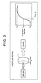
- FIG. 2 is a view for explaining the laser flash method
- FIG. 3 is a view exemplarily showing the structure of a semiconductor device as an application example of the GaN-based material according to the present invention.
- FIG. 4 is a view exemplarily showing the structure of a semiconductor device as an application example of the GaN-based material according to the present invention.
- FIG. 5 is a view showing the arrangement of the HVPE apparatus shown in FIG. 1 in more detail.
- a gallium nitride (GaN)-based material manufacturing method includes a growth step of growing a gallium nitride-based material by HVPE (Hydride Vapor Phase Epitaxial Growth).
- the gallium nitride (GaN)-based material is a III-V compound semiconductor material containing mainly gallium nitride (GaN).
- the material contains mostly gallium (Ga) as a group-III element, and nitrogen (N) as a group-V element.
- the material includes a gallium nitride-based material in which a P- or N-type impurity is doped in order to adjust the conductivity type.
- the GaN-based material is formed on, for example, a GaN substrate, a substrate having layers including a GaN layer, or a substrate such as a sapphire substrate.
- a second element e.g., a member or layer
- a first element e.g., a substrate, member, or layer
- the second element is formed or placed on the first element such that the second element is in contact with the first element, and the case where the second element is formed or placed on one or a plurality of third elements (e.g., members or layers) on the first element.
- FIG. 1 is a view showing an outline of the arrangement of an HVPE apparatus suitable for the GaN-based material manufacturing method of the present invention.
- FIG. 5 is a view showing the arrangement of the HVPE apparatus shown in FIG. 1 in more detail.
- An HVPE apparatus 100 can be constructed as a vertical HVPE apparatus.
- the vertical HVPE apparatus can form a laminar flow more easily than a horizontal HVPE apparatus, and hence is suited to forming a high-quality, high-uniformity epitaxially grown film with a high reproducibility.
- the vertical HVPE apparatus is also advantageous in batch processing (simultaneous growth on a number of substrates).
- the HVPE apparatus 100 can comprise a reaction chamber 10 , a substrate support 30 placed in the reaction chamber 10 to support an underlying substrate (a substrate on which a GaN-based material is to be grown) S on a supporting surface 30 S, a supply chamber 40 constructed to communicate with the reaction chamber 10 , and a heater 20 .
- a carrier gas G 1 , NH 3 gas G 3 , and HCl gas G 4 can be supplied to the supply chamber 40 .
- a vessel 42 containing liquid Ga is placed in the supply chamber 40 .
- the HCl gas G 4 supplied into the supply chamber 40 generates GaCl gas G 2 by reacting with the liquid Ga in the vessel 42 .
- the supply chamber 40 can supply the carrier gas G 1 , GaCl gas G 2 , and NH 3 gas G 3 into the reaction chamber 10 .
- the carrier gas G 1 contains at least H 2 gas.
- the carrier gas G 1 may also contain N 2 gas in addition to H 2 gas.
- the average sectional area of the supply chamber 40 is preferably smaller than that of the reaction chamber 10 , and the average sectional area of the supply chamber 40 is more preferably 2 ⁇ 3 or less the average sectional area of the reaction chamber 10 .
- the average sectional area of the supply chamber 40 is desirably smaller than the sectional area of the reaction chamber 10 in a section including the supporting surface 30 S, and the average sectional area of the supply chamber 40 is more desirably 2 ⁇ 3 or less the sectional area of the reaction chamber 10 in the section including the supporting surface 30 S.
- the flow rates of the carrier gas G 1 , GaCl gas G 2 , and NH 3 gas in the supply chamber 40 can be made higher than those of these gases in the reaction chamber 10 .
- a high-quality gallium nitride-based material having a limited impurity concentration particularly, a gallium nitride-based material having a high thermal conductivity is presumably obtained by adopting the arrangement in which the average sectional area of the supply chamber 40 is smaller than that of the reaction chamber 10 , preferably, the average sectional area of the supply chamber 40 is 2 ⁇ 3 or less the average sectional area of the reaction chamber 10 , or the arrangement in which the average sectional area of the supply chamber 40 is smaller than the sectional area of the reaction chamber 10 in the section including the supporting surface 30 S, preferably, the average sectional area of the supply chamber 40 is 2 ⁇ 3 or less the sectional area of the reaction chamber 10 in the section including the supporting surface 30 S.
- the flow rate of the carrier gas G 1 in the supply chamber 40 is desirably 0.3 (m/min) (inclusive) to 2.5 (m/min) (inclusive), and more desirably 0.5 (m/min) (inclusive) to 1.7 (m/min) (inclusive).
- the flow rate of the carrier gas in the reaction chamber 10 can roughly be calculated based on the ratio of the sectional area of the supply chamber 40 to that of the reaction chamber 10 .
- Oxygen or silicon is readily produced when the inner wall of the reaction chamber 10 or supply chamber 40 is made of quartz. While a gallium nitride-based material is grown, a polycrystal of this gallium nitride-based material can be deposited on the inner wall of the reaction chamber 10 or supply chamber 40 . In this case, the gallium nitride-based material is deposited on the quartz inner wall of the reaction chamber 10 or supply chamber 40 so as to enter the structure of the quartz inner wall. This damages the quarts inner wall and, for example, produces fine scratches in it. If this deposit is removed by an etching gas (e.g., HCl gas), the fine scratches may generate quartz particles. If the quartz particles are thus generated, oxygen or silicon may be mixed in a film of the gallium nitride-based material while the film is grown on the underlying substrate.
- an etching gas e.g., HCl gas
- the growth step of growing a gallium nitride-based material can be performed by supplying the carrier gas G 1 , GaCl gas G 2 , and NH 3 gas G 3 from the supply chamber 40 to the underlying substrate S in the reaction chamber 10 , and setting the growth temperature at 900 (° C.) (inclusive) to 1,200 (° C.) (inclusive), the growth pressure at 8.08 ⁇ 10 4 (Pa) (inclusive) to 1.21 ⁇ 10 5 (Pa) (inclusive), the partial pressure of the GaCl gas G 2 at 1.0 ⁇ 10 2 (Pa) (inclusive) to 1.0 ⁇ 10 4 (Pa) (inclusive), and the partial pressure of the NH 3 gas G 3 at 9.1 ⁇ 10 2 (Pa) (inclusive) to 2.0 ⁇ 0 (Pa) (inclusive).
- the partial pressure of the carrier gas G 1 is the value obtained by subtracting the partial pressures of the GaCl gas G 2 and NH 3 gas G 3 from the growth pressure.
- the growth temperature can be set at 900 (° C.) (inclusive) to 1,200 (° C.) (inclusive) as described above, the growth temperature is preferably 950 (° C.) (inclusive) to 1,150 (° C.) (inclusive), and more preferably 1,000 (° C.) (inclusive) to 1,100 (° C.) (inclusive).
- the growth pressure can be set at 8.08 ⁇ 10 4 (Pa) (inclusive) to 1.21 ⁇ 10 5 (Pa) (inclusive) as described above, the growth pressure is favorably 9.09 ⁇ 10 4 (Pa) (inclusive) to 1.11 ⁇ 10 5 (Pa) (inclusive), and more favorably 9.60 ⁇ 10 4 (Pa) (inclusive) to 1.06 ⁇ 10 5 (Pa) (inclusive).
- the partial pressure of the GaCl gas G 2 can be set at 1.0 ⁇ 10 2 (Pa) (inclusive) to 1.0 ⁇ 10 4 (Pa) (inclusive) as described above, but the partial pressure of the GaCl gas G 2 is desirably 2.0 ⁇ 10 2 (Pa) (inclusive) to 5.6 ⁇ 10 3 (Pa) (inclusive), and more desirably 4.0 ⁇ 10 2 (Pa) (inclusive) to 4.0 ⁇ 10 3 (Pa) (inclusive).
- the partial pressure of the NH 3 gas G 3 can be set at 9.1 ⁇ 10 2 (Pa) (inclusive) to 2.0 ⁇ 10 4 (Pa) (inclusive) as described above, but the partial pressure of the NH 3 gas G 3 is desirably 1.5 ⁇ 10 3 (Pa) (inclusive) to 1.5 ⁇ 10 4 (Pa) (inclusive), and more desirably 2.0 ⁇ 10 3 (Pa) (inclusive) to 1.0 ⁇ 10 4 (Pa) (inclusive).
- H 2 gas partial pressure/((H 2 gas partial pressure)+(N 2 gas partial pressure)) can be set, for example, at 0.05 (inclusive) to 1 (exclusive), is preferably 0.1 (inclusive) to 1 (exclusive), 0.6 (inclusive) to 1 (exclusive), 0.7 (inclusive) to 1 (exclusive), and 0.8 (inclusive) to 1 (exclusive) in this order, and is most preferably 0.9 (inclusive) to 1 (exclusive).
- a GaN material having a thermal conductivity of 2.8 ⁇ 10 2 (W/m ⁇ K) or more at 25 (° C.) can be obtained by performing the growth step by supplying the carrier gas G 1 containing H 2 gas and N 2 gas such that (H 2 gas partial pressure)/((H 2 gas partial pressure)+(N 2 gas partial pressure)) is 0.05 (inclusive) to 1 (exclusive), the GaCl gas G 2 , and the NH 3 gas G 3 from the supply chamber 40 to the reaction chamber 10 , and setting the growth temperature at 900 (° C.) (inclusive) to 1,200 (° C.) (inclusive), the growth pressure at 8.08 ⁇ 10 4 (Pa) (inclusive) to 1.21 ⁇ 10 5 (Pa) (inclusive), the partial pressure of the GaCl gas G 2 at 1.0 ⁇ 10 2 (Pa) (inclusive) to 1.0 ⁇ 10 4 (Pa) (inclusive), and the partial pressure of the NH 3 gas G 3 at 9.1 ⁇ 10 2 (Pa) (inclusive) to 2.0 ⁇ 10
- the growth step is performed by supplying the carrier gas G 1 containing H 2 gas and N 2 gas such that (H 2 gas partial pressure)/((H 2 gas partial pressure)+(N 2 gas partial pressure)) is 0.1 (inclusive) to 1 (exclusive), the GaCl gas G 2 , and the NH 3 gas G 3 from the supply chamber.
- the growth temperature at 900 (° C.) (inclusive) to 1,200 (° C.) (inclusive), the growth pressure at 8.08 ⁇ 10 4 (Pa) (inclusive) to 1.21 ⁇ 10 5 (Pa) (inclusive), the partial pressure of the GaCl gas G 2 at 1.0 ⁇ 10 2 (Pa) (inclusive) to 1.0 ⁇ 10 4 (Pa) (inclusive), and the partial pressure of the NH 3 gas G 3 at 9.1 ⁇ 10 2 (Pa) (inclusive) to 2.0 ⁇ 10 4 (Pa) (inclusive), it is possible to obtain a GaN material having a thermal conductivity of 3.0 ⁇ 10 2 (W/m ⁇ K) or more, more accurately, 306 (W/m ⁇ K) or more at 25 (° C.), a (002)-plane X-ray rocking curve half-width of 300 (arcsec) or less, a (102)-plane X-ray rocking curve half-width of 500 (arcsec) or less, an
- the growth step is performed by supplying the carrier gas G 1 containing H 2 gas and N 2 gas such that (H 2 gas partial pressure)/((H 2 gas partial pressure)+(N 2 gas partial pressure)) is 0.7 (inclusive) to 1 (exclusive), the GaCl gas G 2 , and the NH 3 gas G 3 from the supply chamber 40 to the reaction chamber 10 , and setting the growth temperature at 900 (° C.) (inclusive) to 1,200 (° C.) (inclusive), the growth pressure at 8.08 ⁇ 10 4 (Pa) (inclusive) to 1.21 ⁇ 10 5 (Pa) (inclusive), the partial pressure of the GaCl gas G 2 at 1.0 ⁇ 10 2 (Pa) (inclusive) to 1.0 ⁇ 10 4 (Pa) (inclusive), and the partial pressure of the NH 3 gas G 3 at 9.1 ⁇ 10 2 (Pa) (inclusive) to 2.0 ⁇ 10 4 (Pa) (inclusive), it is possible to obtain a GaN material having a thermal conductivity of 3.3 ⁇ 10 2 (W/m
- gallium nitride-based material or gallium nitride material it is preferable to intentionally dope silicon (in the case of n-type) or the like.
- silicon in the case of n-type
- no impurity it is preferable to intentionally dope no impurity (undope any impurity).
- a sample in which no impurity is intentionally doped is favorable because the sample has a thermal conductivity higher than that of a sample in which an impurity is intentionally doped.
- the impurity are oxygen, silicon, carbon, and hydrogen.
- a desirable impurity concentration of a sample in which no impurity is intentionally doped is as follows.
- the oxygen concentration is preferably less than 1 ⁇ 10 17 (atoms/cm 3 ), more preferably less than 5 ⁇ 10 16 (atoms/cm 3 ), and further preferably less than 2 ⁇ 10 16 (atoms/cm 3 ).
- the SIMS lower detection limit of oxygen is 2 ⁇ 10 16 (atoms/cm 3 ).
- the carbon concentration is preferably less than 5 ⁇ 10 16 (atoms/cm 3 ), more preferably less than 3 ⁇ 10 16 (atoms/cm 3 ), and further preferably less than 1 ⁇ 10 16 (atoms/cm 3 ).
- the SIMS lower detection limit of carbon is 1 ⁇ 10 16 (atoms/cm 3 ).
- the hydrogen concentration is preferably 5 ⁇ 10 17 (atoms/cm 3 ) or less, more preferably 3 ⁇ 10 17 (atoms/cm 3 ) or less, and further preferably less than 1 ⁇ 10 17 (atoms/cm 3 ).
- the SIMS lower detection limit of hydrogen is 1 ⁇ 10 17 (atoms/cm 3 ).
- the silicon concentration is preferably 1 ⁇ 10 17 (atoms/cm 3 ) or less, more preferably 5 ⁇ 10 16 (atoms/cm 3 ) or less, further preferably 5 ⁇ 10 15 (atoms/cm 3 ) or less, and most preferably 1 ⁇ 10 15 (atoms/cm 3 ) or less.
- the SIMS lower detection limit of silicon is 1 ⁇ 10 15 (atoms/cm 3 ).
- the growth step is performed by supplying the carrier gas G 1 practically containing only H 2 , the GaCl gas G 2 , and the NH 3 gas G 3 from the supply chamber 40 to the reaction chamber 10 , and setting the growth temperature at 1,000 (° C.), the growth pressure at 1.01 ⁇ 10 5 (Pa), the partial pressure of the GaCl gas G 2 at 1.11 ⁇ 10 3 (Pa), and the partial pressure of the NH 3 gas G 3 at 4.45 ⁇ 10 3 (Pa), it is possible to obtain a GaN material having a thermal conductivity of 3.5 ⁇ 10 2 (W/m ⁇ K), more accurately, 345 (W/m ⁇ K) at 25 (° C.), and having an oxygen concentration of less than 2 ⁇ 10 16 (atoms/cm 3 ), a carbon concentration of less than 2 ⁇ 10 16 (atoms/cm 3 ), and a hydrogen concentration of less than 1 ⁇ 10 17 (atoms/cm 3 ), that is, having oxygen, carbon, and hydrogen concentrations less than the lower detection limits.
- the growth step is performed by supplying the carrier gas G 1 practically containing only H 2 , the GaCl gas G 2 , and the NH 3 gas G 3 from the supply chamber 40 to the reaction chamber 10 , and setting the growth temperature at 1,100 (° C.), the growth pressure at 1.01 ⁇ 10 5 (Pa), the partial pressure of the GaCl gas G 2 at 1.11 ⁇ 10 3 (Pa), and the partial pressure of the NH 3 gas G 3 at 4.45 ⁇ 10 3 (Pa), it is possible to obtain a GaN material having a thermal conductivity of 3.7 ⁇ 10 2 (W/m ⁇ K), more accurately, 371 (W/m ⁇ K) at 25 (° C.), and having an oxygen concentration of less than 2 ⁇ 10 16 (atoms/cm 3 ), a carbon concentration of less than 2 ⁇ 10 16 (atoms/cm 3 ), and a hydrogen concentration of less than 1 ⁇ 10 17 (atoms/cm 3 ), that is, having oxygen and hydrogen concentrations less than the lower detection limits.
- the growth step is performed by supplying the carrier gas G 1 practically containing only H 2 , the GaCl gas G 2 , and the NH 3 gas G 3 from the supply chamber 40 to the reaction chamber 10 , and setting the growth temperature at 1,070 (° C.), the growth pressure at 1.01 ⁇ 10 5 (Pa), the partial pressure of the GaCl gas G 2 at 1.11 ⁇ 10 3 (Pa), and the partial pressure of the NH 3 gas G 3 at 4.45 ⁇ 10 3 (Pa), it is possible to obtain a GaN material having a thermal conductivity of 3.8 ⁇ 10 2 (W/m ⁇ K), more accurately, 380 (W/m ⁇ K) at 25 (° C.), a (002)-plane X-ray rocking curve half-width of 62.0 (arcsec), and a (102)-plane X-ray rocking curve half-width of 98.9 (arcsec), and having an oxygen concentration of less than 2 ⁇ 10 16 (atoms/cm 3 ), a carbon concentration of less than 1 ⁇ 10 16
- the (002)-plane X-ray rocking curve half-width of the GaN-based material is preferably 300 (arcsec) or less, more preferably 200 (arcsec) or less, and further preferably 100 (arcsec) or less. Under the conditions described above, it is possible to obtain a GaN-based material having a (002)-plane X-ray rocking curve half-width of 62.0 (arcsec).
- the (102)-plane X-ray rocking curve half-width of the GaN-based material is preferably 300 (arcsec) or less, more preferably 200 (arcsec) or less, and further preferably 100 (arcsec) or less. Under the conditions described above, it is possible to obtain a GaN-based material having a (102)-plane X-ray rocking curve half-width of 98.9 (arcsec).
- the thermal conductivity described above was evaluated in accordance with the laser flash method. To directly obtain the thermal conductivity, it is necessary to prepare a large sample and perform measurement over a long time period.
- the laser flash method is a measurement method of calculating the thermal diffusivity from the change in temperature on the back surface of a disk-like sample S having a diameter of 10 (mm) and a thickness of about 1 to 5 (mm), after evenly heating the front surface of the sample S with a laser beam having a pulse width of a few hundred ⁇ s.
- the back-surface temperature of the sample S heated with pulses rises as shown in FIG. 2 , and converges to a predetermined value as the internal temperature distribution of the sample S is made even.
- the laser flash method can measure a small sample within a short time, uses a simple analytical method, and can perform measurements from room temperature to a high temperature of 200 (° C.) or more. Accordingly, the laser flash method is widely used as a standard practical thermal diffusivity measurement method.
- Equation (1) was applied by assuming that the density of GaN was 6.15 (g/cm 3 ) and the specific heat of GaN was 40.8 (J/mol ⁇ K) (Barin, I., O. Knaeke, and 0. Kubasehewski, Thermochemical Properties of Inorganic Substrates, Springer-Verlag, Berlin, 1977).
- the measurement value of the thermal diffusivity can be corrected by using a standard sample.
- a substrate or member made of the GaN-based material according to the present invention is suitable as an epitaxial film growing substrate of a device such as a semiconductor laser, light emitting diode, or electronic device.
- a substrate or member made of the GaN-based material according to the present invention is suitable as a mounting member of a device such as a semiconductor laser, light emitting diode, or electronic device.
- FIGS. 3 and 4 are views exemplarily showing the structures of semiconductor devices as application examples of the GaN-based material according to the present invention.
- a semiconductor product 200 comprises a semiconductor device 210 , submount 230 , and heat sink 240 .
- the semiconductor device 210 is fixed to the heat sink 240 with the submount 230 being interposed between them. Heat generated by the semiconductor device 210 is transferred to the heat sink 240 via the submount 230 , and mainly dissipated from the heat sink 240 .
- the semiconductor device 210 has a multilayered structure 214 including active layers.
- the multilayered structure 214 can be supported by, for example, a substrate 212 .
- the substrate 212 is, for example, a template substrate for growing the multilayered structure 214 .
- the substrate 212 is also made of the gallium nitride-based material having a high thermal conductivity according to the present invention, the heat generated by this semiconductor device can be efficiently transferred through the substrate 212 because the heat is principally generated by the multilayered structure 214 including the active layers.
- a substrate or member made of the GaN-based material according to the present invention can be used as at least one of the substrate 212 , submount 230 , and heat sink 240 .
- a semiconductor product 300 comprises a semiconductor device 210 , and a heat sink 250 fixed to the semiconductor device 210 . Heat generated by the semiconductor device 210 is transferred to the heat sink 250 and dissipated from it.
- the semiconductor device 210 has a multilayered structure 214 including active layers.
- the multilayered structure 214 can be supported by, for example, a substrate 212 .
- the substrate 212 is, for example, a template substrate for growing the multilayered structure 214 .
- the heat generated by this semiconductor device can be efficiently transferred through the substrate 212 because the heat is principally generated by the multilayered structure 214 including the active layers.
- a substrate or member made of the GaN-based material according to the present invention can be used as one or both of the substrate 212 and heat sink 250 .
- the manufacturing method of the present invention it is possible to obtain a GaN-based material having a thermal conductivity of 250 (W/m ⁇ K) or more at 25 (° C.), and obtain a GaN-based material having a thermal conductivity of 300 (W/m ⁇ K) or more or 345 (W/m ⁇ K) or more at 25 (° C.) by adjusting the growth conditions.
- the theoretical limit of the thermal conductivity of an ideal GaN crystal is 410 W/m ⁇ K.
- a GaN-based material having a high thermal conductivity as described above is useful as some or all of the substrate 212 , submount 230 , and heat sinks 240 and 250 . This makes it possible to efficiently dissipate heat generated in the active layers, and suppress the temperature rise in the active layers. This temperature rise suppressing effect is effective to hold the device characteristics or performance (e.g., the optical output) of the device almost constant in constant-current driving or low-voltage driving, and also helps improve the device reliability.
- a GaN-based material having a high thermal conductivity greatly helps improve the element characteristics and long-term reliability of particularly a high-power device, for example, a light emitting device such as a (super)high-output semiconductor laser or (super)high-luminance light emitting diode, or an electronic device such as a power switching element or high-power, high-frequency electronic element.
- a GaN-based material having a high thermal conductivity is used as a support substrate (including a crystal growing substrate), it is possible to achieve element superior in element characteristics and long-term reliability even in junction down assembling.
- semiconductor device can include an electronic device, optical device, and the like.
- semiconductor device can include, for example, a Hall element usable as a position sensor, a microwave field effect transistor (FET), a high electron mobility transistor (HEMT), and a hetero-junction bipolar transistor (HBT).
- semiconductor device can include a light emitting diode (LED), laser diode (LD), and the like.
- a member made of a material such as GaN having a high hardness is preferably divided or shaped by using cleavage, because it is difficult to divide the member by dicing. Since a member made of a single-crystal GaN-based material has a specific crystal plane, a rectangular parallelepiped or cube can be obtained by cleavage.
- the crystal system of a GaN-based material formed is desirably a Wultzite structure, although it may also be a cubic system.
- a GaN-based material formed desirably has a single-crystal structure, although it may also have a polycrystalline structure. This is so because lattice vibration causes thermal diffusion, and a single-crystal structure has a high thermal diffusion efficiency.
- a single-crystal structure can be processed by cleavage or the like by using a specific crystal plane. This makes it possible to obtain a rectangular parallelepiped or cubic member (e.g., a heat sink or submount) relatively easily.
- a GaN-based material is grown on an underlying substrate by HVPE.
- a semiconductor substrate is preferably used as the underlying substrate, although either a semiconductor substrate or dielectric substrate can be used.
- the underlying substrate is favorably a substrate having a lattice constant close to that of a GaN-based material crystal layer to be grown on the substrate. It is particularly favorable to use a compound semiconductor substrate in which the lattice constant is 0.30 to 0.36 nm in the a-axis direction, and 0.48 to 0.58 nm in the c-axis direction.
- the underling substrate desirably has a crystal structure belonging to the cubic system or hexagonal system.
- the cubic-system substrate it is possible to use, for example, Si, GaAs, InGaAs, GaP, InP, ZnSe, ZnTe, or CdTd.
- the hexagonal-system substrate it is possible to use, for example, sapphire, SiC, GaN, spinel, or ZnO.
- An off substrate may also be used as the underlying substrate.
- a sapphire substrate in which the (ABCD) plane or a plane slightly inclined from the (ABCD) plane is a plane used to grow a nitride semiconductor crystal layer.
- A, B, C, and D indicate natural numbers.
- the angle of this slight inclination is normally 0° to 10°, preferably 0° to 0.5°, and more preferably 0° to 0.2°.
- “Equivalent planes” are planes in which the atomic arrangements crystallographically become the same when the planes are rotated 90° in the cubic system or 60° in the hexagonal system.
- a GaN-based material can be directly grown on the underlying substrate in accordance with the present invention. However, it is also possible to form an underlying layer on the underlying substrate, and grow a GaN-based material on the underlying layer in accordance with the present invention.
- the underlying layer can be formed by, for example, molecular beam epitaxy (MBE), metal organic chemical vapor deposition (MOCVD), PLD (Pulsed Laser Deposition; J. Cryst. Growth, 237/239 (2002) 1153), or HVPE.
- MBE molecular beam epitaxy
- MOCVD metal organic chemical vapor deposition
- PLD Pulsed Laser Deposition; J. Cryst. Growth, 237/239 (2002) 1153
- HVPE HydroVPE
- crystal growth can be controlled with accuracy on the molecular-layer level although the growth rate is low, so a layered nitride semiconductor crystal superior in surface properties is obtained. Also, crystal growth can be performed at a relatively low temperature by MBE, the original substrate such as sapphire or zinc oxide can maintain a stable state without being affected by gases used in the formation of an initial nitride semiconductor layer and/or Ga-containing nitride semiconductor crystal layer.
- the underlying layer By forming the underlying layer like this, it is possible to improve the crystal state and surface state of a GaN-based material layer grown on the underlying layer.
- PLD can grow crystals at a temperature (e.g., room temperature) lower than that of MBE, does not use ammonia gas, and hence is advantageous when using a highly reactive substrate such as sapphire or zinc oxide.
- a temperature e.g., room temperature
- apparatuses capable of growing crystals on more than fifty 2-inch substrates at once are available for MOCVD and HVPE. Accordingly, MOCVD and HVPE are very superior in mass-production properties to other growth methods, and have industrial priority over other methods.
- the thickness of the underlying layer is not particularly limited, provided that a GaN-based material layer formed on the underlying layer can stably have a good crystallinity and good surface properties. From the viewpoint of productivity, the thickness of the underlying layer is normally 0.1 to 5.0 ( ⁇ m), and preferably 0.3 to 2.0 ( ⁇ m).
- the surface roughness (Ra) of the underlying layer or underlying substrate is preferably 1 (nm) or less, more preferably 0.8 (nm) or less, and further preferably 0.7 nm or less.
- the surface roughness herein mentioned is the central line average roughness (Ra), and can be obtained by measuring the roughness of the surface by AFM (Atomic Force Microscopy).
- a procedure of forming an underlying layer on an underlying substrate made of sapphire, and forming a GaN-based material layer on the underlying layer will be exemplarily explained below.
- an underlying layer having a thickness of normally 0.1 ( ⁇ m) to 5.0 ( ⁇ m), and preferably 0.3 ( ⁇ m) to 2.0 ( ⁇ m) is formed on a sapphire substrate by, for example, MBE, MOCVD, PLD, or HVPE.
- GaN-based material layer is formed on the underlying layer by HVPE in accordance with the present invention.
- Ga is supplied into the reaction chamber 10 as GaCl gas generated by the reaction between Ga and HCl.
- a nitrogen material is supplied into the reaction chamber 10 as NH 3 gas.
- the reaction temperature when generating GaCl by the reaction between Ga and HCl is preferably about 850 (° C.).
- the substrate on which the GaN-based material layer is grown is unloaded from the reaction chamber 10 once and cooled, it is also possible to perform another step such as etching or polishing using an acid or the like, or laser slicing.
- a surface treatment such as polishing may also be performed on the surface of the GaN-based material layer as needed.
- Laser lift-off may also be used as a method of removing the GaN-based material layer from the underlying substrate. More specifically, after the GaN-based material layer is grown, a laser is emitted to the interface between the underlying substrate and GaN-based material layer to expose the interface to a high temperature, thereby removing particularly the nitrogen component of gallium nitride. Since, therefore, Ga remaining in the interface can be removed with hydrochloric acid or the like, the underlying substrate can easily be removed.
- the underlying substrate can also be removed by the stress generated between the GaN-based material layer and underlying substrate while the temperature is decreased after the layer is grown in a growth apparatus.
- a sapphire substrate 430 ( ⁇ m) in thickness and 2 inches in diameter having a (0001) surface was prepared as an underlying substrate, and cleaned with an organic solvent as pre-preprocessing. After that, an underlying GaN layer having a thickness of 2 ( ⁇ m) was grown on the underlying substrate by using an MOCVD apparatus.
- the substrate having the underlying GaN layer grown on it was placed in the reaction chamber 10 of an HVPE apparatus, and the reaction temperature was raised to 1,070 (° C.).
- the carrier gas G 1 practically containing only H 2 , the GaCl gas G 2 as the reaction product of Ga and HCl, and the NH 3 gas G 3 were supplied onto the GaN layer, a GaN layer was grown on the underlying GaN layer for about 15 hrs.
- the growth pressure was set at 1.01 ⁇ 10 5 (Pa)
- the partial pressure of GaCl gas G 2 was set at 1.11 ⁇ 10 3 (Pa)
- the partial pressure of the NH 3 gas G 3 was set at 4.45 ⁇ 10 3 (Pa).
- the sapphire substrate was removed from the substrate on which the GaN layer was grown.
- an Si-doped the carrier concentration: n-type, 4 ⁇ 10 17 (atoms/cm 3 ), the hole measurement value
- self-supporting GaN single-crystal substrate about 1,060 ( ⁇ m) thick was obtained.
- the oxygen, carbon, and hydrogen impurity concentrations were respectively less than 2 ⁇ 10 16 (atoms/cm 3 ), less than 1 ⁇ 10 16 (atoms/cm 3 ) and less than 1 ⁇ 10 17 (atoms/cm 3 ), that is, all the impurity concentrations were less than the detection limits.
- the threading dislocation density measured by CL (Cathode Luminescence) or AFM was 2 ⁇ 10 6 (dislocations/cm 2 ).
- the (002) X-ray rocking curve half-width and (102) X-ray rocking curve half-width of the obtained GaN single-crystal substrate were measured and found to be 62.0 (arcsec) and 98.9 (arcsec), respectively.
- a square plate-like GaN single-crystal sample of 10 (mm) side having a thickness of 1 (mm) was formed by polishing and shaping the two surfaces of the obtained GaN single-crystal substrate.
- the laser flash measurement sample was obtained by forming gold films about 200 (nm) thick on the two surfaces of the GaN single-crystal sample, and further forming a carbon film (the thickness was less than 1 ⁇ m) on the laser irradiation surface.
- the obtained laser flash measurement sample was measured by the laser flash method by using the TC-700 full-automatic laser flash thermal constant measurement apparatus available from ULVAC-RIKO, and the TD-AL thermal diffusivity measurement standard material available from JAPAN FINE CERAMICS CENTER, and t 1/2 data analysis was performed. Consequently, the thermal diffusivity at room temperature (25° C.) was 127 (mm 2 /sec).
- the calculation was performed by assuming that the density of GaN was 6.15 (g/cm 3 ) and the specific heat of GaN was 40.8 (J/mol ⁇ K) (Barin, I., O. Knaeke, and O. Kubasehewski, Thermochemical Properties of Inorganic Substrates, Springer-Verlag, Berlin, 1977).
- the thermal conductivity of the GaN single crystal obtained by this method was 386 (W/m ⁇ K) at room temperature.
- a GaN layer was grown on an underlying GaN layer under the same conditions as in Example 1 except that the reaction temperature was set at 1,000 (° C.).
- a sapphire substrate was removed from a substrate on which the GaN layer was grown.
- an Si-doped the carrier concentration: n-type, 4 ⁇ 10 17 (atoms/cm 3 ), the hole measurement value
- self-supporting GaN single-crystal substrate about 1,060 ( ⁇ m) thick was obtained.
- the oxygen, carbon, and hydrogen impurity concentrations were respectively less than 2 ⁇ 10 16 (atoms/cm 3 ), 2 ⁇ 10 16 (atoms/cm 3 ), and less than 1 ⁇ 10 17 (atoms/cm 3 ), that is, the oxygen and hydrogen concentrations were less than the detection limits.
- the threading dislocation density measured by CL (Cathode Luminescence) or AEM was 5 ⁇ 10 6 (dislocations/cm 2 ).
- a square plate-like GaN single-crystal sample of 10 (mm) side having a thickness of 1 (mm) was formed by polishing and shaping the two surfaces of the obtained GaN single-crystal substrate.
- the thermal conductivity of the GaN single crystal obtained in the same manner as in Example 1 was 345 (W/m ⁇ K) at room temperature.
- a GaN layer was grown on an underlying GaN layer under the same conditions as in Example 1 except that the reaction temperature was set at 1,100 (° C.).
- a sapphire substrate was removed from a substrate on which the GaN layer was grown.
- an Si-doped the carrier concentration: n-type, 4 ⁇ 10 17 (atoms/cm 3 ), the hole measurement value
- self-supporting GaN single-crystal substrate about 1,060 ( ⁇ m) thick was obtained.
- the oxygen, carbon, and hydrogen impurity concentrations were respectively less than 2 ⁇ 10 16 (atoms/cm 3 ), less than 1 ⁇ 10 16 (atoms/cm 3 ), and less than 1 ⁇ 10 17 (atoms/cm 3 ), that is, all the impurity concentrations were less than the detection limits.
- the threading dislocation density measured by CL (Cathode Luminescence) or AFM was 3 ⁇ 10 6 (dislocations/cm 2 ).
- a square plate-like GaN single-crystal sample of 10 (mm) side having a thickness of 1 (mm) was formed by polishing and shaping the two surfaces of the obtained GaN single-crystal substrate.
- the thermal conductivity of the GaN single crystal obtained in the same manner as in Example 1 was 371 (W/m ⁇ K) at room temperature.
- a sapphire substrate 430 ( ⁇ m) in thickness and 2 inches in diameter having a (0001) surface was prepared as an underlying substrate, and cleaned with an organic solvent as pre-preprocessing. After that, an underlying GaN layer having a thickness of 2 ( ⁇ m) was grown on the underlying substrate by using an MOCVD apparatus.
- the substrate having the underlying GaN layer grown on it was placed in the reaction chamber 10 of an HVPE apparatus, and the reaction temperature was raised to 1,070 (° C.).
- the growth pressure was set at 1.01 ⁇ 10 5 (Pa)
- the partial pressure of GaCl gas G 2 was set at 1.11 ⁇ 10 3 (Pa)
- the partial pressure of the NH 3 gas G 3 was set at 4.45 ⁇ 10 3 (Pa).
- the gas flow rate was 0.931 (m/min) in the supply chamber 40 .
- the sapphire substrate was removed from the substrate on which the GaN layer was grown.
- an Si-doped the carrier concentration: n-type, 3.5 ⁇ 10 17 (atoms/cm 3 ), the hole measurement value) self-supporting GaN single-crystal substrate about 1,643 ( ⁇ m) thick was obtained.
- the oxygen, carbon, and hydrogen impurity concentrations were respectively less than 3 ⁇ 10 16 (atoms/cm 3 ), 5 ⁇ 10 16 (atoms/cm 3 ), and less than 5 ⁇ 10 16 (atoms/cm 3 ), that is, the oxygen concentration was less than the detection limit.
- the threading dislocation density measured by CL (Cathode Luminescence) or AFM was 5 ⁇ 10 6 (dislocations/cm 2 ).
- a plate-like GaN single-crystal sample was formed by polishing and shaping the two surfaces of the obtained GaN single-crystal substrate.
- a laser flash measurement sample was formed following the same procedure as in Example 1.
- the thermal diffusivity at room temperature (25° C.) was 109 (mm 2 /sec).
- the thermal conductivity of the GaN single crystal obtained in the same manner as in Example 1 was 327 (W/m ⁇ K) at room temperature.
- a sapphire substrate 430 ( ⁇ m) in thickness and 2 inches in diameter having a (0001) surface was prepared as an underlying substrate, and cleaned with an organic solvent as pre-preprocessing. After that, an underlying GaN layer having a thickness of 2 ( ⁇ m) was grown on the underlying substrate by using an MOCVD apparatus.
- the substrate having the underlying GaN layer grown on it was placed in the reaction chamber 10 of an HVPE apparatus, and the reaction temperature was raised to 975 (° C.).
- the growth pressure was set at 1.01 ⁇ 10 5 (Pa)
- the partial pressure of GaCl gas G 2 was set at 1.11 ⁇ 10 3 (Pa)
- the partial pressure of the NH 3 gas G 3 was set at 4.45 ⁇ 10 3 (Pa).
- the gas flow rate was 0.931 (m/min) in the supply chamber 40 .
- the sapphire substrate was removed from the substrate on which the GaN layer was grown.
- an Si-doped the carrier concentration: n-type, 8.9 ⁇ 10 17 (atoms/cm 3 ), the hole measurement value
- self-supporting GaN single-crystal substrate about 1,271 ( ⁇ m) thick was obtained.
- the oxygen, carbon, and hydrogen impurity concentrations were respectively 2 ⁇ 10 18 (atoms/cm 3 ), 1 ⁇ 10 17 (atoms/cm 3 ) and 1 ⁇ 10 17 (atoms/cm 3 ).
- the threading dislocation density measured by CL (Cathode Luminescence) or AFM was 5 ⁇ 10 6 (dislocations/cm 2 ).
- a plate-like GaN single-crystal sample was formed by polishing and shaping the two surfaces of the obtained GaN single-crystal substrate.
- a laser flash measurement sample was formed following the same procedure as in Example 1.
- the thermal diffusivity at room temperature (25° C.) was 102 (mm 2 /sec).
- the thermal conductivity of the GaN single crystal obtained in the same manner as in Example 1 was 306 (W/m ⁇ K) at room temperature.
- a sapphire substrate 430 ( ⁇ m) in thickness and 2 inches in diameter having a (0001) surface was prepared as an underlying substrate, and cleaned with an organic solvent as pre-preprocessing. After that, an underlying GaN layer having a thickness of 2 ( ⁇ m) was grown on the underlying substrate by using an MOCVD apparatus.
- the substrate having the underlying GaN layer grown on it was placed in a reaction chamber of an HVPE apparatus in which a supply chamber and the reaction chamber had the same sectional area, and the reaction temperature was raised to 1,010 (° C.).
- the carrier gas G 1 practically containing only N 2 gas
- the NH 3 gas G 3 were supplied onto the GaN layer, a GaN layer was grown on the underlying GaN layer for about 15 hrs.
- the growth pressure was set at 1.01 ⁇ 10 5 (Pa)
- the partial pressure of GaCl gas G 2 was set at 2.91 ⁇ 10 2 (Pa)
- the partial pressure of the NH 3 gas G 3 was set at 1.17 ⁇ 10 4 (Pa).
- the gas flow rate was 0.133 (m/min) in the space above the underlying substrate.
- the sapphire substrate was removed from the substrate on which the GaN layer was grown.
- an n-type (the carrier concentration: 9.0 ⁇ 10 17 (atoms/cm 3 ), the hole measurement value) self-supporting GaN single-crystal substrate about 1,072 ( ⁇ m) thick was obtained.
- the oxygen, carbon, and hydrogen impurity concentrations were respectively 1 ⁇ 10 19 (atoms/cm 3 ), 6 ⁇ 10 16 (atoms/cm 3 ), and 6 ⁇ 10 16 (atoms/cm 3 ).
- a plate-like GaN single-crystal sample was formed by polishing and shaping the two surfaces of the obtained GaN single-crystal substrate.
- a laser flash measurement sample was formed following the same procedure as in Example 1.
- the thermal diffusivity at room temperature (25° C.) was 84.3 (mm 2 /sec).
- the thermal conductivity of the GaN single crystal obtained in the same manner as in Example 1 was 253 (W/m ⁇ K) at room temperature.
- the present invention can provide a gallium nitride material having a thermal conductivity of 3.0 ⁇ 10 2 (W/m ⁇ K) or more at 25 (° C.).
- the concentration of silicon as an impurity was a relatively high concentration (4 ⁇ 10 17 cm ⁇ 3 ).
- a GaN-based material having a high thermal conductivity was formed by HVPE.
- HVPE solvothermal method
- liquid phase epitaxy liquid phase epitaxy
- metal organic chemical vapor deposition a GaN-based material is formed such that the impurity concentrations of oxygen, carbon, hydrogen, and silicon fall within the ranges described above.
- GaN gallium nitride
- GaN gallium nitride
- GaN gallium nitride
- III-V compound semiconductor material mostly containing gallium (Ga) as a group-III element and nitrogen (N) as a group-V element.
Landscapes
- Engineering & Computer Science (AREA)
- Chemical & Material Sciences (AREA)
- Materials Engineering (AREA)
- Power Engineering (AREA)
- Condensed Matter Physics & Semiconductors (AREA)
- General Physics & Mathematics (AREA)
- Manufacturing & Machinery (AREA)
- Computer Hardware Design (AREA)
- Microelectronics & Electronic Packaging (AREA)
- Physics & Mathematics (AREA)
- Crystallography & Structural Chemistry (AREA)
- Metallurgy (AREA)
- Organic Chemistry (AREA)
- General Chemical & Material Sciences (AREA)
- Chemical Kinetics & Catalysis (AREA)
- Inorganic Chemistry (AREA)
- Crystals, And After-Treatments Of Crystals (AREA)
- Semiconductor Lasers (AREA)
- Led Devices (AREA)
- Chemical Vapour Deposition (AREA)
Applications Claiming Priority (5)
| Application Number | Priority Date | Filing Date | Title |
|---|---|---|---|
| JP2006-067907 | 2006-03-13 | ||
| JP2006067907 | 2006-03-13 | ||
| JP2007056353A JP4187175B2 (ja) | 2006-03-13 | 2007-03-06 | 窒化ガリウム系材料の製造方法 |
| JP2007-056353 | 2007-03-06 | ||
| PCT/JP2007/054591 WO2007119319A1 (ja) | 2006-03-13 | 2007-03-08 | 窒化ガリウム系材料及びその製造方法 |
Publications (2)
| Publication Number | Publication Date |
|---|---|
| US20090081110A1 US20090081110A1 (en) | 2009-03-26 |
| US7794541B2 true US7794541B2 (en) | 2010-09-14 |
Family
ID=38609128
Family Applications (3)
| Application Number | Title | Priority Date | Filing Date |
|---|---|---|---|
| US12/282,961 Active US7794541B2 (en) | 2006-03-13 | 2007-03-08 | Gallium nitride-based material and method of manufacturing the same |
| US12/707,173 Abandoned US20100140536A1 (en) | 2006-03-13 | 2010-02-17 | Gallium nitride-based material |
| US12/719,465 Abandoned US20100162945A1 (en) | 2006-03-13 | 2010-03-08 | Gallium nitride-based material and method of manufacturing the same |
Family Applications After (2)
| Application Number | Title | Priority Date | Filing Date |
|---|---|---|---|
| US12/707,173 Abandoned US20100140536A1 (en) | 2006-03-13 | 2010-02-17 | Gallium nitride-based material |
| US12/719,465 Abandoned US20100162945A1 (en) | 2006-03-13 | 2010-03-08 | Gallium nitride-based material and method of manufacturing the same |
Country Status (6)
| Country | Link |
|---|---|
| US (3) | US7794541B2 (ja) |
| EP (1) | EP1995357A1 (ja) |
| JP (1) | JP4187175B2 (ja) |
| KR (2) | KR101424292B1 (ja) |
| TW (1) | TW200802761A (ja) |
| WO (1) | WO2007119319A1 (ja) |
Cited By (3)
| Publication number | Priority date | Publication date | Assignee | Title |
|---|---|---|---|---|
| US20110108887A1 (en) * | 2009-11-06 | 2011-05-12 | Nitek, Inc. | Multilayer barrier iii-nitride transistor for high voltage electronics |
| US20110155049A1 (en) * | 2009-12-30 | 2011-06-30 | Cbl Technologies, Inc. | Modern hydride vapor-phase epitaxy system & methods |
| US20120034149A1 (en) * | 2010-06-10 | 2012-02-09 | Sumitomo Electric Industries, Ltd. | GaN-CRYSTAL FREE-STANDING SUBSTRATE AND METHOD FOR PRODUCING THE SAME |
Families Citing this family (22)
| Publication number | Priority date | Publication date | Assignee | Title |
|---|---|---|---|---|
| JP2008297191A (ja) * | 2007-05-02 | 2008-12-11 | Sumitomo Electric Ind Ltd | 窒化ガリウム基板及び窒化ガリウム層の形成方法 |
| JP5018423B2 (ja) | 2007-11-20 | 2012-09-05 | 住友電気工業株式会社 | Iii族窒化物半導体結晶基板および半導体デバイス |
| KR20100049934A (ko) | 2008-11-04 | 2010-05-13 | 현대자동차주식회사 | 가솔린 직접 분사 엔진 |
| US8017963B2 (en) * | 2008-12-08 | 2011-09-13 | Cree, Inc. | Light emitting diode with a dielectric mirror having a lateral configuration |
| EP2377974A4 (en) | 2009-01-08 | 2014-11-19 | Mitsubishi Chem Corp | PROCESS FOR PRODUCING NITRIDE CRYSTAL, NITRIDE CRYSTAL, AND MANUFACTURING DEVICE THEREOF |
| JP5434111B2 (ja) * | 2009-02-06 | 2014-03-05 | 三菱化学株式会社 | 自立基板の製造方法 |
| JP5544723B2 (ja) * | 2009-02-06 | 2014-07-09 | 三菱化学株式会社 | ショットキーダイオードおよびショットキーダイオードの製造方法 |
| KR100943091B1 (ko) * | 2009-04-07 | 2010-02-18 | 주식회사 시스넥스 | 질화갈륨 단결정 성장을 위한 수소화기상증착기 |
| FR2968830B1 (fr) | 2010-12-08 | 2014-03-21 | Soitec Silicon On Insulator | Couches matricielles ameliorees pour le depot heteroepitaxial de materiaux semiconducteurs de nitrure iii en utilisant des procedes hvpe |
| EP2770089A4 (en) | 2011-10-21 | 2015-09-02 | Mitsubishi Chem Corp | METHOD FOR PRODUCING A NITRIDE SEMICONDUCTOR CRYSTAL OF A GROUP 13 METAL OF THE PERIODIC TABLE AND A NITRIDE SEMI-CONDUCTIVE CRYSTAL OF A GROUP 13 METAL OF THE PERIODIC TABLE PRODUCED BY SAID PRODUCTION PROCESS |
| JP2013173652A (ja) * | 2012-02-27 | 2013-09-05 | Tokuyama Corp | 自立基板の製造方法 |
| JP2013177275A (ja) * | 2012-02-28 | 2013-09-09 | Mitsubishi Chemicals Corp | Iii族窒化物結晶の製造方法およびiii族窒化物半結晶 |
| EP3056592B1 (en) * | 2013-10-09 | 2021-12-01 | Osaka University | Method for producing group iii nitride crystal and apparatus for producing group iii nitride crystal |
| EP3998370A1 (en) * | 2015-03-30 | 2022-05-18 | Tosoh Corporation | Gallium nitride-based film and method for manufacturing same |
| JP6740623B2 (ja) * | 2015-04-24 | 2020-08-19 | 東ソー株式会社 | 窒化ガリウム系膜ならびにその製造方法 |
| JP6916719B2 (ja) * | 2017-11-17 | 2021-08-11 | 株式会社トクヤマ | Iii族窒化物単結晶積層体の製造方法及びiii族窒化物単結晶積層体 |
| CN110777432B (zh) * | 2018-07-30 | 2023-09-29 | 住友化学株式会社 | 氮化物晶体 |
| CN110777433B (zh) * | 2018-07-30 | 2023-09-29 | 住友化学株式会社 | 氮化物晶体 |
| CN116288724A (zh) | 2018-08-17 | 2023-06-23 | 三菱化学株式会社 | n型GaN结晶、GaN晶片以及GaN结晶、GaN晶片和氮化物半导体器件的制造方法 |
| JP7326759B2 (ja) * | 2019-02-06 | 2023-08-16 | 三菱ケミカル株式会社 | GaN単結晶製造方法 |
| JP7379931B2 (ja) * | 2019-08-23 | 2023-11-15 | 三菱ケミカル株式会社 | c面GaN基板 |
| KR102536978B1 (ko) * | 2021-11-10 | 2023-05-26 | 신정훈 | 질화갈륨 단결정 성장을 위한 하이드라이드 기상 증착 장비 |
Citations (14)
| Publication number | Priority date | Publication date | Assignee | Title |
|---|---|---|---|---|
| JPH1012555A (ja) * | 1996-06-24 | 1998-01-16 | Sharp Corp | 窒化物系化合物半導体結晶の製造方法 |
| JPH11265884A (ja) * | 1998-03-18 | 1999-09-28 | Hitachi Ltd | 半導体製造方法ならびに半導体製造装置 |
| JP2000252217A (ja) | 1999-03-01 | 2000-09-14 | Sumitomo Electric Ind Ltd | 化合物半導体の製造方法 |
| US6159287A (en) | 1999-05-07 | 2000-12-12 | Cbl Technologies, Inc. | Truncated susceptor for vapor-phase deposition |
| JP2001181097A (ja) | 1999-12-22 | 2001-07-03 | Nec Corp | 窒化物の気相成長装置 |
| JP2001335399A (ja) * | 2000-05-24 | 2001-12-04 | Nikko Materials Co Ltd | 気相成長方法 |
| WO2002044443A1 (en) | 2000-11-30 | 2002-06-06 | North Carolina State University | Methods and apparatus for producing m'n based materials |
| JP2003078084A (ja) | 2001-08-30 | 2003-03-14 | Sony Corp | ヒートシンクおよびサブマウント |
| US20030211710A1 (en) | 2002-03-26 | 2003-11-13 | Kazumasa Hiramatsu | Method of manufacturing III-V group compound semiconductor |
| JP2004039810A (ja) | 2002-07-02 | 2004-02-05 | Nec Corp | Iii族窒化物半導体基板およびその製造方法 |
| JP2005119921A (ja) | 2003-10-17 | 2005-05-12 | Hitachi Cable Ltd | Iii族窒化物半導体基板およびその製造方法 |
| JP2005263609A (ja) | 2003-12-26 | 2005-09-29 | Hitachi Cable Ltd | Iii−v族窒化物系半導体基板及びその製造ロット、並びにiii−v族窒化物系半導体デバイス及びその製造方法 |
| WO2006003381A1 (en) | 2004-06-30 | 2006-01-12 | Wang Nang Wang | Deposition technique for producing high quality compound semiconductor materials |
| JP2007217227A (ja) | 2006-02-16 | 2007-08-30 | Sumitomo Electric Ind Ltd | GaN結晶の製造方法、GaN結晶基板および半導体デバイス |
Family Cites Families (12)
| Publication number | Priority date | Publication date | Assignee | Title |
|---|---|---|---|---|
| US6617235B2 (en) * | 1995-03-30 | 2003-09-09 | Sumitomo Chemical Company, Limited | Method of manufacturing Group III-V compound semiconductor |
| JP3591710B2 (ja) * | 1999-12-08 | 2004-11-24 | ソニー株式会社 | 窒化物系iii−v族化合物層の成長方法およびそれを用いた基板の製造方法 |
| JP2001181907A (ja) | 1999-12-22 | 2001-07-03 | Mikio Kuzuu | 磁石付きブラジャー |
| US6660606B2 (en) * | 2000-09-29 | 2003-12-09 | Canon Kabushiki Kaisha | Semiconductor-on-insulator annealing method |
| US7053413B2 (en) * | 2000-10-23 | 2006-05-30 | General Electric Company | Homoepitaxial gallium-nitride-based light emitting device and method for producing |
| JP3631724B2 (ja) * | 2001-03-27 | 2005-03-23 | 日本電気株式会社 | Iii族窒化物半導体基板およびその製造方法 |
| PL207400B1 (pl) * | 2001-06-06 | 2010-12-31 | Ammono Społka Z Ograniczoną Odpowiedzialnością | Sposób i urządzenie do otrzymywania objętościowego monokryształu azotku zawierającego gal |
| US6897495B2 (en) * | 2001-10-31 | 2005-05-24 | The Furukawa Electric Co., Ltd | Field effect transistor and manufacturing method therefor |
| US7170095B2 (en) * | 2003-07-11 | 2007-01-30 | Cree Inc. | Semi-insulating GaN and method of making the same |
| JP2005101475A (ja) * | 2003-08-28 | 2005-04-14 | Hitachi Cable Ltd | Iii−v族窒化物系半導体基板及びその製造方法 |
| US7009215B2 (en) * | 2003-10-24 | 2006-03-07 | General Electric Company | Group III-nitride based resonant cavity light emitting devices fabricated on single crystal gallium nitride substrates |
| JP2005209803A (ja) * | 2004-01-21 | 2005-08-04 | Sumitomo Electric Ind Ltd | GaN結晶基板の製造方法 |
-
2007
- 2007-03-06 JP JP2007056353A patent/JP4187175B2/ja active Active
- 2007-03-08 KR KR1020087020693A patent/KR101424292B1/ko active IP Right Grant
- 2007-03-08 EP EP07738081A patent/EP1995357A1/en not_active Withdrawn
- 2007-03-08 US US12/282,961 patent/US7794541B2/en active Active
- 2007-03-08 KR KR1020137020916A patent/KR20130098438A/ko not_active Application Discontinuation
- 2007-03-08 WO PCT/JP2007/054591 patent/WO2007119319A1/ja active Application Filing
- 2007-03-13 TW TW096108521A patent/TW200802761A/zh unknown
-
2010
- 2010-02-17 US US12/707,173 patent/US20100140536A1/en not_active Abandoned
- 2010-03-08 US US12/719,465 patent/US20100162945A1/en not_active Abandoned
Patent Citations (19)
| Publication number | Priority date | Publication date | Assignee | Title |
|---|---|---|---|---|
| JPH1012555A (ja) * | 1996-06-24 | 1998-01-16 | Sharp Corp | 窒化物系化合物半導体結晶の製造方法 |
| JPH11265884A (ja) * | 1998-03-18 | 1999-09-28 | Hitachi Ltd | 半導体製造方法ならびに半導体製造装置 |
| JP2000252217A (ja) | 1999-03-01 | 2000-09-14 | Sumitomo Electric Ind Ltd | 化合物半導体の製造方法 |
| JP2002544109A (ja) | 1999-05-07 | 2002-12-24 | シービーエル テクノロジーズ インコーポレイテッド | 気相堆積のための切頭サセプター |
| US6159287A (en) | 1999-05-07 | 2000-12-12 | Cbl Technologies, Inc. | Truncated susceptor for vapor-phase deposition |
| JP2001181097A (ja) | 1999-12-22 | 2001-07-03 | Nec Corp | 窒化物の気相成長装置 |
| JP2001335399A (ja) * | 2000-05-24 | 2001-12-04 | Nikko Materials Co Ltd | 気相成長方法 |
| JP2004523450A (ja) | 2000-11-30 | 2004-08-05 | ノース・キャロライナ・ステイト・ユニヴァーシティ | M’nベース物質の生成装置及び生成方法 |
| WO2002044443A1 (en) | 2000-11-30 | 2002-06-06 | North Carolina State University | Methods and apparatus for producing m'n based materials |
| JP2003078084A (ja) | 2001-08-30 | 2003-03-14 | Sony Corp | ヒートシンクおよびサブマウント |
| US20030211710A1 (en) | 2002-03-26 | 2003-11-13 | Kazumasa Hiramatsu | Method of manufacturing III-V group compound semiconductor |
| JP2004006568A (ja) | 2002-03-26 | 2004-01-08 | Sumitomo Chem Co Ltd | 3−5族化合物半導体の製造方法 |
| US6946308B2 (en) | 2002-03-26 | 2005-09-20 | Sumitomo Chemical Company, Limited | Method of manufacturing III-V group compound semiconductor |
| JP2004039810A (ja) | 2002-07-02 | 2004-02-05 | Nec Corp | Iii族窒化物半導体基板およびその製造方法 |
| JP2005119921A (ja) | 2003-10-17 | 2005-05-12 | Hitachi Cable Ltd | Iii族窒化物半導体基板およびその製造方法 |
| US20060270200A1 (en) | 2003-10-17 | 2006-11-30 | Hitachi Cable, Ltd. | III group nitride semiconductor substrate, substrate for group III nitride semiconductor device, and fabrication methods thereof |
| JP2005263609A (ja) | 2003-12-26 | 2005-09-29 | Hitachi Cable Ltd | Iii−v族窒化物系半導体基板及びその製造ロット、並びにiii−v族窒化物系半導体デバイス及びその製造方法 |
| WO2006003381A1 (en) | 2004-06-30 | 2006-01-12 | Wang Nang Wang | Deposition technique for producing high quality compound semiconductor materials |
| JP2007217227A (ja) | 2006-02-16 | 2007-08-30 | Sumitomo Electric Ind Ltd | GaN結晶の製造方法、GaN結晶基板および半導体デバイス |
Non-Patent Citations (7)
| Title |
|---|
| "GaN Substrates Technology", CREE Materials, http://www.cree.com/products/gan-tech.htm, pp. 1-2 and 1, (2005). |
| J. Bai, et al., "(0001) oriented GaN epilayer grown on (1120) sapphire by MOCVD", Journal of Crystal Growth, vol. 231, 2001, pp. 41-47. |
| J. Zou, et al., "Thermal conductivity of GaN films: Effects of impurities and dislocations", Journal of Applied Physics, vol. 92, No. 5, Sep. 1, 2002, pp. 2534-2539. |
| K., sichel E. et al., "Thermal Conductivity of GaN, 25-360 K", J. Phys. Chem. Solids., Pergamon Press, vol. 38, p. 330, (1977). |
| Kawamura et al., Investigation of thermal conductivity of GaN by molecular dynamics, 2005, Journal of Crystal Growth, 284, 197-202. |
| Liu, Weili et al., "Increased thermal conductivity of free-standing low-dislocation-density GaN films", Phys. Stat. Sol. (a), Rapid Research Letters, vol. 202, No. I 12, pp. R135-R137, (2005). |
| Zhang et al., Electron cyclotron resonance etching characteristics of GaN in SiCI4/Ar, 1196, Appl. Phys. Lett., 68, 367-369. |
Cited By (7)
| Publication number | Priority date | Publication date | Assignee | Title |
|---|---|---|---|---|
| US20110108887A1 (en) * | 2009-11-06 | 2011-05-12 | Nitek, Inc. | Multilayer barrier iii-nitride transistor for high voltage electronics |
| US8541817B2 (en) | 2009-11-06 | 2013-09-24 | Nitek, Inc. | Multilayer barrier III-nitride transistor for high voltage electronics |
| US20110155049A1 (en) * | 2009-12-30 | 2011-06-30 | Cbl Technologies, Inc. | Modern hydride vapor-phase epitaxy system & methods |
| US8465587B2 (en) * | 2009-12-30 | 2013-06-18 | Cbl Technologies, Inc. | Modern hydride vapor-phase epitaxy system and methods |
| US20120034149A1 (en) * | 2010-06-10 | 2012-02-09 | Sumitomo Electric Industries, Ltd. | GaN-CRYSTAL FREE-STANDING SUBSTRATE AND METHOD FOR PRODUCING THE SAME |
| US8574364B2 (en) * | 2010-06-10 | 2013-11-05 | Sumitomo Electric Industries, Ltd. | GaN-crystal free-standing substrate and method for producing the same |
| US9153742B2 (en) | 2010-06-10 | 2015-10-06 | Sumitomo Electric Industries, Ltd. | GaN-crystal free-standing substrate and method for producing the same |
Also Published As
| Publication number | Publication date |
|---|---|
| KR20130098438A (ko) | 2013-09-04 |
| JP4187175B2 (ja) | 2008-11-26 |
| EP1995357A1 (en) | 2008-11-26 |
| KR101424292B1 (ko) | 2014-08-01 |
| KR20080108980A (ko) | 2008-12-16 |
| US20100140536A1 (en) | 2010-06-10 |
| US20100162945A1 (en) | 2010-07-01 |
| WO2007119319A1 (ja) | 2007-10-25 |
| JP2007277077A (ja) | 2007-10-25 |
| TW200802761A (en) | 2008-01-01 |
| US20090081110A1 (en) | 2009-03-26 |
Similar Documents
| Publication | Publication Date | Title |
|---|---|---|
| US7794541B2 (en) | Gallium nitride-based material and method of manufacturing the same | |
| JP5105258B2 (ja) | 窒化ガリウム系材料及びその製造方法 | |
| EP2313543B1 (en) | Growth of planar and semi-polar {1 1-2 2} gallium nitride with hydride vapor phase epitaxy (hvpe) | |
| US8465588B2 (en) | Ammonothermal method for growth of bulk gallium nitride | |
| US6440823B1 (en) | Low defect density (Ga, Al, In)N and HVPE process for making same | |
| JP4462251B2 (ja) | Iii−v族窒化物系半導体基板及びiii−v族窒化物系発光素子 | |
| US20140191244A1 (en) | METHOD FOR CONDUCTIVITY CONTROL OF (Al,In,Ga,B)N | |
| US9362115B2 (en) | Nitride semiconductor wafer, nitride semiconductor element, and method for manufacturing nitride semiconductor wafer | |
| US20070040219A1 (en) | III-V group nitride system semiconductor self-standing substrate, method of making the same and III-V group nitride system semiconductor wafer | |
| EP2684988A1 (en) | Base, substrate with gallium nitride crystal layer, and process for producing same | |
| JP2004524250A (ja) | 窒化ガリウム材料および方法 | |
| CN104518062B (zh) | 制造半导体发光器件的方法 | |
| US20070215901A1 (en) | Group III-V nitride-based semiconductor substrate and method of fabricating the same | |
| US20060160345A1 (en) | Innovative growth method to achieve high quality III-nitride layers for wide band gap optoelectronic and electronic devices | |
| JP2009500862A (ja) | ミスカット基板上のレーザダイオード配向 | |
| US7902047B2 (en) | Dual chamber system providing simultaneous etch and deposition on opposing substrate sides for growing low defect density epitaxial layers | |
| Sawaki et al. | Semi-polar GaN LEDs on Si substrate | |
| US6339014B1 (en) | Method for growing nitride compound semiconductor | |
| JPH10290051A (ja) | 半導体装置とその製造方法 | |
| JP2004119423A (ja) | 窒化ガリウム結晶基板、その製造方法、窒化ガリウム系半導体素子および発光ダイオード | |
| US20140183579A1 (en) | Miscut semipolar optoelectronic device | |
| JP2014192246A (ja) | 半導体基板およびそれを用いた半導体素子 | |
| WO2013157014A1 (en) | Group iii-nitride semiconducting material and a method of manufacturing the same | |
| JP2009208989A (ja) | 化合物半導体基板およびその製造方法 | |
| JP2020070196A (ja) | 窒化物半導体層の成長方法 |
Legal Events
| Date | Code | Title | Description |
|---|---|---|---|
| AS | Assignment |
Owner name: TOHOKU UNIVERSITY, JAPAN Free format text: ASSIGNMENT OF ASSIGNORS INTEREST;ASSIGNORS:SHIBATA, HIROYUKI;WASEDA, YOSHIO;SHIMOYAMA, KENJI;AND OTHERS;REEL/FRAME:021558/0405;SIGNING DATES FROM 20080630 TO 20080711 Owner name: MITSUBISHI CHEMICAL CORPORATION, JAPAN Free format text: ASSIGNMENT OF ASSIGNORS INTEREST;ASSIGNORS:SHIBATA, HIROYUKI;WASEDA, YOSHIO;SHIMOYAMA, KENJI;AND OTHERS;REEL/FRAME:021558/0405;SIGNING DATES FROM 20080630 TO 20080711 Owner name: TOHOKU UNIVERSITY, JAPAN Free format text: ASSIGNMENT OF ASSIGNORS INTEREST;ASSIGNORS:SHIBATA, HIROYUKI;WASEDA, YOSHIO;SHIMOYAMA, KENJI;AND OTHERS;SIGNING DATES FROM 20080630 TO 20080711;REEL/FRAME:021558/0405 Owner name: MITSUBISHI CHEMICAL CORPORATION, JAPAN Free format text: ASSIGNMENT OF ASSIGNORS INTEREST;ASSIGNORS:SHIBATA, HIROYUKI;WASEDA, YOSHIO;SHIMOYAMA, KENJI;AND OTHERS;SIGNING DATES FROM 20080630 TO 20080711;REEL/FRAME:021558/0405 |
|
| STCF | Information on status: patent grant |
Free format text: PATENTED CASE |
|
| FPAY | Fee payment |
Year of fee payment: 4 |
|
| AS | Assignment |
Owner name: MITSUBISHI RAYON CO., LTD., JAPAN Free format text: MERGER;ASSIGNOR:MITSUBISHI CHEMICAL CORPORATION;REEL/FRAME:043750/0207 Effective date: 20170401 |
|
| AS | Assignment |
Owner name: MITSUBISHI CHEMICAL CORPORATION, JAPAN Free format text: CHANGE OF NAME;ASSIGNOR:MITSUBISHI RAYON CO., LTD.;REEL/FRAME:043750/0834 Effective date: 20170401 |
|
| MAFP | Maintenance fee payment |
Free format text: PAYMENT OF MAINTENANCE FEE, 8TH YEAR, LARGE ENTITY (ORIGINAL EVENT CODE: M1552) Year of fee payment: 8 |
|
| MAFP | Maintenance fee payment |
Free format text: PAYMENT OF MAINTENANCE FEE, 12TH YEAR, LARGE ENTITY (ORIGINAL EVENT CODE: M1553); ENTITY STATUS OF PATENT OWNER: LARGE ENTITY Year of fee payment: 12 |