US7548271B2 - Flash device, camera device and method and program thereof for the elimination of wasteful power consumption therein - Google Patents
Flash device, camera device and method and program thereof for the elimination of wasteful power consumption therein Download PDFInfo
- Publication number
- US7548271B2 US7548271B2 US10/965,309 US96530904A US7548271B2 US 7548271 B2 US7548271 B2 US 7548271B2 US 96530904 A US96530904 A US 96530904A US 7548271 B2 US7548271 B2 US 7548271B2
- Authority
- US
- United States
- Prior art keywords
- main capacitor
- switch
- voltage
- charging
- camera device
- Prior art date
- Legal status (The legal status is an assumption and is not a legal conclusion. Google has not performed a legal analysis and makes no representation as to the accuracy of the status listed.)
- Expired - Fee Related, expires
Links
- 238000000034 method Methods 0.000 title description 4
- 230000008030 elimination Effects 0.000 title 1
- 238000003379 elimination reaction Methods 0.000 title 1
- 239000003990 capacitor Substances 0.000 claims abstract description 86
- 238000001514 detection method Methods 0.000 claims description 11
- 240000007320 Pinus strobus Species 0.000 description 20
- 238000010586 diagram Methods 0.000 description 4
- 230000005611 electricity Effects 0.000 description 4
- 230000003287 optical effect Effects 0.000 description 3
- 230000000694 effects Effects 0.000 description 2
- 230000006870 function Effects 0.000 description 2
- 229910052724 xenon Inorganic materials 0.000 description 2
- FHNFHKCVQCLJFQ-UHFFFAOYSA-N xenon atom Chemical compound [Xe] FHNFHKCVQCLJFQ-UHFFFAOYSA-N 0.000 description 2
- HBBGRARXTFLTSG-UHFFFAOYSA-N Lithium ion Chemical compound [Li+] HBBGRARXTFLTSG-UHFFFAOYSA-N 0.000 description 1
- BQCADISMDOOEFD-UHFFFAOYSA-N Silver Chemical compound [Ag] BQCADISMDOOEFD-UHFFFAOYSA-N 0.000 description 1
- 238000013144 data compression Methods 0.000 description 1
- 230000006837 decompression Effects 0.000 description 1
- 230000000994 depressogenic effect Effects 0.000 description 1
- 239000004973 liquid crystal related substance Substances 0.000 description 1
- 229910001416 lithium ion Inorganic materials 0.000 description 1
- 229920001690 polydopamine Polymers 0.000 description 1
- 230000002035 prolonged effect Effects 0.000 description 1
- 238000001454 recorded image Methods 0.000 description 1
- 229910052709 silver Inorganic materials 0.000 description 1
- 239000004332 silver Substances 0.000 description 1
Images



Classifications
-
- H—ELECTRICITY
- H05—ELECTRIC TECHNIQUES NOT OTHERWISE PROVIDED FOR
- H05B—ELECTRIC HEATING; ELECTRIC LIGHT SOURCES NOT OTHERWISE PROVIDED FOR; CIRCUIT ARRANGEMENTS FOR ELECTRIC LIGHT SOURCES, IN GENERAL
- H05B41/00—Circuit arrangements or apparatus for igniting or operating discharge lamps
- H05B41/14—Circuit arrangements
- H05B41/30—Circuit arrangements in which the lamp is fed by pulses, e.g. flash lamp
-
- H—ELECTRICITY
- H05—ELECTRIC TECHNIQUES NOT OTHERWISE PROVIDED FOR
- H05B—ELECTRIC HEATING; ELECTRIC LIGHT SOURCES NOT OTHERWISE PROVIDED FOR; CIRCUIT ARRANGEMENTS FOR ELECTRIC LIGHT SOURCES, IN GENERAL
- H05B41/00—Circuit arrangements or apparatus for igniting or operating discharge lamps
- H05B41/14—Circuit arrangements
- H05B41/30—Circuit arrangements in which the lamp is fed by pulses, e.g. flash lamp
- H05B41/32—Circuit arrangements in which the lamp is fed by pulses, e.g. flash lamp for single flash operation
-
- H—ELECTRICITY
- H04—ELECTRIC COMMUNICATION TECHNIQUE
- H04N—PICTORIAL COMMUNICATION, e.g. TELEVISION
- H04N23/00—Cameras or camera modules comprising electronic image sensors; Control thereof
- H04N23/60—Control of cameras or camera modules
- H04N23/65—Control of camera operation in relation to power supply
- H04N23/651—Control of camera operation in relation to power supply for reducing power consumption by affecting camera operations, e.g. sleep mode, hibernation mode or power off of selective parts of the camera
-
- H—ELECTRICITY
- H04—ELECTRIC COMMUNICATION TECHNIQUE
- H04N—PICTORIAL COMMUNICATION, e.g. TELEVISION
- H04N23/00—Cameras or camera modules comprising electronic image sensors; Control thereof
- H04N23/56—Cameras or camera modules comprising electronic image sensors; Control thereof provided with illuminating means
Definitions
- the present invention relates to a flash device, a camera device with the flash device, and a method and program thereof.
- the strobe built in a camera is configured to step up a voltage of a battery stored in a camera main body, as is well known, and charge a main capacitor with the voltage, and at the time of picking up an image, it gives a charge stored in the main capacitor to a discharge tube (such as a xenon tube) via a trigger coil in accordance with a trigger signal, so as to discharge it to emit light.
- a capacitance of the main capacitor is about 50 ⁇ F to 200 ⁇ F, which fluctuates depending on a difference in an amount of light which is to be emitted by the strobe.
- a charge lost as described above can be expressed by (1 ⁇ 2) ⁇ C ⁇ V 2 wherein C is the capacitance of the main capacitor and V is the charging voltage, and electric power for this is wasted from the battery.
- the present invention has been attained in view of the problems heretofore posed, and its object is to provide a flash device, a camera device with the flash device, and a method and program thereof which can eliminate wasteful power consumption and extend a life of a power supply battery.
- the invention according to claim 1 provides a flash device which emits fill light at the time of image pickup by use of electric power charging a main capacitor, and the flash device comprises: step-down means for stepping down charging voltage of the main capacitor and supplying the voltage as the electric power elsewhere; a switch which performs a switching operation to switch the main capacitor from a charging circuit of the main capacitor to the step-down means so as to connect the main capacitor to the step-down means; and control means for causing the switch to perform the switching operation as required.
- the flash device comprises detection means for detecting the charging voltage of the main capacitor; and when the charging voltage detected by the detection means is a prescribed voltage or higher, the control means causes the switch to perform the switching operation.
- the step-down means has a plurality of feeding paths which supplies the stepped down power of the main capacitor elsewhere.
- the step-down means supplies the stepped down power of the main capacitor to a charging circuit of a charging battery used for charging the main capacitor.
- the step-down means supplies the stepped down power of the main capacitor to other circuits which are supplied with electric power from the charging battery used for charging the main capacitor.
- the step-down means supplies the stepped down power of the main capacitor to the charging circuit of the charging battery used for charging the main capacitor and to the other circuits which are supplied with electric power from the charging battery.
- a camera device which is equipped with a flash device to emit light at a time of image pickup by using electric power charged in a main capacitor.
- the camera device includes: (i) a step-down circuit which steps down a charged voltage of the main capacitor and supplies the voltage to perform a housing operation of a lens of the camera device; (ii) a switch which performs a switching operation to switch the main capacitor from a charging circuit of the main capacitor to the step-down circuit; and (iii) a control device which, when an image pickup standby mode which requires preparation for the emission of the light is terminated, controls the switch to perform the switching operation.
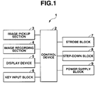
- FIG. 1 is a block diagram of a digital camera showing one embodiment of the present invention
- FIG. 2 is a block diagram showing essential parts of the digital camera
- FIG. 3 is a graph showing set values of charging voltages in a main capacitor
- FIG. 4 is a flowchart showing an operation when a power key is turned on in the digital camera.
- FIG. 5 is a flowchart showing an operation when the power key is turned off in the digital camera.
- FIG. 1 is a block diagram showing a schematic configuration of a digital camera 1 according to the present invention.
- the digital camera 1 is constituted of a control device 2 , and an image pickup section 3 , an image recording section 4 , a display device 5 , a key input block 6 , a strobe block 7 , a step-down block 8 and a power supply block 9 whose operations are controlled by the control device.
- the control device 2 , the strobe block 7 , the step-down block 8 and the power supply block 9 actualize a flash device of the present invention.
- the control device 2 has a ROM storing a predetermined program and a RAM for working, and is a microcomputer comprising various kinds of digital signal processing functions including data compression and decompression.
- the control device 2 operates in accordance with the program stored in the ROM to function as control means of the present invention.
- the image pickup section 3 includes, for example, an optical system which forms an image of a subject, a lens motor provided in a drive mechanism of the optical system, a image pickup device such as a CCD which picks up the image of the subject formed by the optical system through photoelectric transfer, and a signal processing circuit which, for example, amplifies a pickup image signal output by the image pickup device and converts it to a digital signal.
- the image pickup section 3 sends the digital pickup image signal to the control device 2 .
- the image recording section 4 is constituted of a flash memory, a card memory detachable from a main body, and the like, which records the image of the subject which is picked up by the image pickup section 3 and then compressed by the control device 2 in a method such as JPEG. In addition, the image recording section 4 records other data if necessary.
- the display device 5 includes a liquid crystal display and other drive circuits, and it displays the image picked up by the image pickup section 3 as a through image in an image pickup standby state where a shutter key is not depressed in a REC mode for image pickup, while it displays the image read from the image recording section 4 in a PLAY mode for recorded image reproduction.
- the key input block 6 is constituted of various kinds of operation keys such as a shutter key, an image selection key, a mode key to set an operation mode, and power switch. Scan signals are sequentially sent to the key input block 6 from the control device 2 by interrupt processing, and when a user operates any of the operation keys, it is detected by the control device 2 .
- FIG. 2 is a block diagram showing details of the strobe block 7 , the step-down block 8 and the power supply block 9 .
- the power supply block 9 is constituted of a charging battery 91 of lithium ion or the like which is a power supply of the digital camera 1 ; a charging circuit 92 which supplies the charging battery 91 with electric energy supplied from a domestic power supply or the like via an AC adaptor 100 ; and a power supply circuit 93 which supplies the electric power of the charging battery 91 to other blocks 101 .
- the strobe block 7 is constituted of a step-up/charging circuit 72 which steps up a voltage of 3.4 V of the charging battery 91 to about 300 V and supplies the stepped up voltage to a main capacitor 71 ; a light emitting section 73 including a discharge tube such as a xenon tube as a light source, a trigger coil and a drive element for stepping up a voltage of the main capacitor 71 to about 2 KV or higher so that the discharge tube discharges electricity; and a strobe control circuit 74 which controls operations of the step-up/charging circuit 72 and the light emitting section 73 .
- the strobe control circuit 74 causes the drive element to drive the trigger coil in accordance with a trigger signal sent from the control device 2 at the time of image pickup so that the discharge tube discharges electricity, thereby emitting fill light for image pickup.
- the strobe control circuit 74 is detection means of the present invention for detecting the charging voltage of the main capacitor 71 via the step-up/charging circuit 72 , and controls an operation of charging the main capacitor 71 in the step-up/charging circuit 72 .
- control is performed so that the charging voltage of the main capacitor 71 will be over a value (100 V) that enables the discharge tube to emit light and below an upper limit value (330 V) (see FIG. 3 ).
- the step-down block 8 is constituted of a step-down circuit 81 which steps down the voltage of the main capacitor 71 to supply it to the power supply block 9 ; and a switch 82 which switches a connection of the main capacitor 71 to the step-up/charging circuit 72 of the strobe block 7 (side b in the drawing) or to the step-down circuit 81 (side a in the drawing). Power is fed from the step-down circuit 81 to the power supply block 9 via a first power feeder 8 a whose output voltage is set to 5 V and a second power feeder 8 b whose output voltage is set to 4.2 V.
- the first power feeder 8 a (5 V side) is connected to the charging circuit 92
- the second power feeder 8 b (4.2 V side) is connected to the power supply circuit 93 .
- operations of the step-down circuit 81 and the switch 82 are controlled by the control device 2 , and the step-down circuit 81 is controlled so that it maintains a connection state with the power supply block 9 via one of the first power feeder 8 a or the second power feeder 8 b.
- FIG. 4 is a flowchart showing contents of the interrupt processing executed when the control device 2 detects an ON operation of the power key.
- the control device 2 causes the power supply circuit 93 to start supplying power to the components shown in FIG. 1 at the start of the processing (step SA 1 ), and then immediately sets the switch 82 of the step-down block 8 to the side a (step SA 2 ). Subsequently, the control device 2 detects a state of the operation mode set by the mode key (step SA 3 ), and merely stops the processing if the operation mode is not the REC mode (NO in step SA 4 ), and then moves to processing of other operation modes such as the PLAY mode.
- step SA 4 when the REC mode is set (YES in step SA 4 ), the control device 2 performs initial setting of various parameters necessary for the operation in the REC mode (step SA 5 ), and after a turning-out operation of a lens in the image pickup section 3 (step SA 6 ), the control device 2 causes the strobe control circuit 74 to start charging the main capacitor 71 (step SA 7 ).
- FIG. 5 is a flowchart showing the interrupt processing executed when the control device 2 detects an OFF operation of the power key.
- the control device 2 detects the state of the operation mode set by the mode key at the start of the processing (step SB 1 ), and immediately stops power supply to the components from the power supply circuit 93 (step SB 10 ) if the operation mode is not the REC mode (NO in step SB 2 ), and terminates the processing.
- the control device 2 performs processing corresponding to other operation modes such as the PLAY mode, which is not shown.
- the control device 2 determines whether or not the charging voltage of the main capacitor 71 detected by the strobe control circuit 74 is a predetermined voltage or higher, that is, 100 V or higher in the present embodiment (step SB 3 ).
- the control device 2 sets the switch 82 of the step-down block 8 to the side b, and causes the step-down circuit 81 to start supplying electricity to the power supply circuit 93 of the power supply block 9 via the second power feeder 8 b (step SB 4 ).
- the image pickup section 3 performs a housing operation of the lens (step SB 5 ), and various parameters necessary for the operation in the REC mode are stored in the flash memory or the like (step SB 6 ). Further, the control device 2 causes the step-down circuit 81 to start supplying electricity to the charging circuit 92 of the power supply block 9 via the first power feeder 8 b , that is, to start an operation of charging the charging battery 91 (step SB 8 ), and then stops the power supply to the components from the power supply circuit 93 (step SB 10 ), thereby finishing the processing. In other words, the operation for turning off the power supply is performed by use of the power remaining in the main capacitor 71 , and remaining power is returned to the charging battery 91 .
- step SB 3 when the result of determination in step SB 3 described above is NO and the charging voltage of the main capacitor 71 at the moment of turning off the power key is below 100 V, for example, immediately after an image is picked up by use of the strobe or when a slight amount of time has passed since the power key is turned on, only the housing operation of the lens described above and storage of the various parameters are performed (steps SB 8 , SB 9 ), and the power supply to the each component from the power supply circuit 93 is stopped (step SB 10 ), thus terminating the processing. In other words, the low charging state of the main capacitor 71 is maintained as it is.
- the power remaining in the main capacitor 71 is automatically utilized for the operation to turn off the power supply if the charging voltage of the main capacitor 71 is 100 V or higher, and remaining power is returned to the charging battery 91 . It is thus possible to effectively utilize the power remaining in the main capacitor 71 which has conventionally been lost due to natural discharge. Therefore, wasteful power consumption can be eliminated, and a life of a charging battery, that is, continuous use time per battery change or charging can be extended. Moreover, the power remaining in the main capacitor 71 can be directly utilized for the operation to turn off the power supply, so that it is highly effectively utilized.
- the charging voltage of the main capacitor 71 is below 100 V, this charging voltage is maintained as it is, so that time to charge the main capacitor 71 when the power supply is turned on next time can be prevented from being unnecessarily longer. Therefore, it is possible not only to prolong the battery life mentioned above but also to minimize the inconvenience caused thereby.
- the power of the main capacitor 71 may be unconditionally utilized without its charge state (remaining power) being checked. However, if the voltage supplied from the step-down circuit 81 to the power supply block 9 is insufficient, the power from the main capacitor is not used.
- supply ends of the power of the main capacitor 71 are the power supply circuit 93 and the charging circuit 92 and these supply ends can be switched, but this is not a limitation, and a configuration in which the remaining power is always supplied to both of the supply ends may also be possible.
- the supply ends need different voltages as in the present embodiment, it is convenient to use the remaining power if the configuration capable of switching is adopted.
- the operation in which the power supply is turned off in the state where the REC mode is set has been mainly described in the present embodiment.
- the user switches the mode from the REC mode to other operation modes such as the PLAY mode or a movie mode for picking up moving images, it can be more effective if the remaining power of the main capacitor 71 is utilized for operations in those operation modes. It is also effective when prohibition of the use of the strobe is set in the REC mode.
- the remaining power of the main capacitor 71 is used for the charging operation of the charging battery 91 and other operations in the present embodiment, but such a configuration may also be possible that the remaining power is used only for the charging operation of the charging battery 91 .
- the remaining power of the main capacitor 71 fluctuates, so that if, for example, it is used for a plurality of operations, these operations may be switched depending on the remaining power.
- the present invention is employed for the digital camera which stores the image of the subject picked up by the image pickup device as digital data
- it can also be employed for mobile telephones with cameras, PDAs with cameras, and silver cameras with the strobes as long as those are camera devices equipped with the strobes.
- the same effects can also be obtained as in the present embodiment.
- more remarkable effects can be obtained in the mobile telephones with cameras because capacity of its power supply is significantly limited.
- the flash device of the present invention does not always need to be built in the digital camera, and it may be a separate flash device that is separately connected to the digital camera or the like.
Landscapes
- Engineering & Computer Science (AREA)
- Multimedia (AREA)
- Signal Processing (AREA)
- Studio Devices (AREA)
- Stroboscope Apparatuses (AREA)
- Camera Bodies And Camera Details Or Accessories (AREA)
- Discharge-Lamp Control Circuits And Pulse- Feed Circuits (AREA)
Applications Claiming Priority (3)
| Application Number | Priority Date | Filing Date | Title |
|---|---|---|---|
| JP2002-381365 | 2002-12-27 | ||
| JP2002381365A JP4561032B2 (ja) | 2002-12-27 | 2002-12-27 | 閃光装置、及び閃光装置付きカメラ装置、その方法とプログラム |
| PCT/JP2003/016024 WO2004062325A1 (en) | 2002-12-27 | 2003-12-15 | Flash device, camera device and method and program thereof for the elimination of wasteful power consumption therein |
Related Parent Applications (1)
| Application Number | Title | Priority Date | Filing Date |
|---|---|---|---|
| PCT/JP2003/016024 Continuation WO2004062325A1 (en) | 2002-12-27 | 2003-12-15 | Flash device, camera device and method and program thereof for the elimination of wasteful power consumption therein |
Publications (2)
| Publication Number | Publication Date |
|---|---|
| US20050062877A1 US20050062877A1 (en) | 2005-03-24 |
| US7548271B2 true US7548271B2 (en) | 2009-06-16 |
Family
ID=32708488
Family Applications (1)
| Application Number | Title | Priority Date | Filing Date |
|---|---|---|---|
| US10/965,309 Expired - Fee Related US7548271B2 (en) | 2002-12-27 | 2004-10-14 | Flash device, camera device and method and program thereof for the elimination of wasteful power consumption therein |
Country Status (8)
| Country | Link |
|---|---|
| US (1) | US7548271B2 (de) |
| EP (1) | EP1576861A1 (de) |
| JP (1) | JP4561032B2 (de) |
| KR (1) | KR100709696B1 (de) |
| CN (1) | CN1692681A (de) |
| AU (1) | AU2003288749A1 (de) |
| TW (1) | TWI240843B (de) |
| WO (1) | WO2004062325A1 (de) |
Cited By (1)
| Publication number | Priority date | Publication date | Assignee | Title |
|---|---|---|---|---|
| US8771085B1 (en) | 2010-08-06 | 2014-07-08 | Arthur C. Clyde | Modular law enforcement baton |
Families Citing this family (7)
| Publication number | Priority date | Publication date | Assignee | Title |
|---|---|---|---|---|
| JP4478599B2 (ja) * | 2005-03-22 | 2010-06-09 | キヤノン株式会社 | 撮像装置 |
| KR100764658B1 (ko) | 2006-05-18 | 2007-10-08 | 삼성전자주식회사 | 이동통신 단말기의 포털 사이트 접속 장치 및 방법 |
| JP5590792B2 (ja) * | 2008-12-16 | 2014-09-17 | キヤノン株式会社 | 照明装置、撮像装置及び充電制御方法 |
| JP5718667B2 (ja) * | 2011-02-15 | 2015-05-13 | 京セラ株式会社 | 携帯端末、充電制御プログラムおよび充電制御方法 |
| JP6465555B2 (ja) * | 2014-03-25 | 2019-02-06 | キヤノン株式会社 | 撮像装置、電子機器、カメラシステム、制御方法、およびプログラム |
| JP6425474B2 (ja) * | 2014-09-10 | 2018-11-21 | キヤノン株式会社 | 発光制御装置、その制御方法、および制御プログラム、並びに撮像装置 |
| US10938294B1 (en) * | 2018-04-02 | 2021-03-02 | Amazon Technologies, Inc. | Doorbell circuit architecture |
Citations (11)
| Publication number | Priority date | Publication date | Assignee | Title |
|---|---|---|---|---|
| US4333718A (en) | 1980-01-16 | 1982-06-08 | Rollei Of America, Inc. | Photographic flash control circuitry having selectively operable internal sensor |
| JPS6413779A (en) | 1987-07-08 | 1989-01-18 | Oki Electric Ind Co Ltd | Multiterminal type josephson element |
| US5227831A (en) * | 1990-08-17 | 1993-07-13 | Olympus Optical Co., Ltd. | Auto-zooming camera apparatus having advanced photographing-magnification setting and displaying functions |
| US5852358A (en) | 1996-12-11 | 1998-12-22 | The Texas A&M University System | Capactive power circuit |
| JPH11252447A (ja) | 1998-03-04 | 1999-09-17 | Sony Corp | カメラ装置 |
| US6054814A (en) | 1998-09-08 | 2000-04-25 | Eastman Kodak Company | Camera flash charging apparatus for low cost single use camera |
| JP2002287218A (ja) | 2001-03-26 | 2002-10-03 | Sanyo Electric Co Ltd | カメラ |
| US6571061B2 (en) * | 2000-08-30 | 2003-05-27 | Pentax Corporation | Uniform flash-emission controller |
| JP2003280071A (ja) | 2002-03-25 | 2003-10-02 | Fuji Photo Film Co Ltd | フラッシュ付カメラ |
| US20040027480A1 (en) * | 1996-06-25 | 2004-02-12 | Nikon Corporation | Information processing apparatus and method for operating same |
| US20040264223A1 (en) * | 2003-06-30 | 2004-12-30 | Intel Corporation | Switched capacitor power converter |
-
2002
- 2002-12-27 JP JP2002381365A patent/JP4561032B2/ja not_active Expired - Fee Related
-
2003
- 2003-12-15 WO PCT/JP2003/016024 patent/WO2004062325A1/en not_active Ceased
- 2003-12-15 KR KR1020047017303A patent/KR100709696B1/ko not_active Expired - Fee Related
- 2003-12-15 EP EP03780758A patent/EP1576861A1/de not_active Withdrawn
- 2003-12-15 CN CNA2003801004283A patent/CN1692681A/zh active Pending
- 2003-12-15 AU AU2003288749A patent/AU2003288749A1/en not_active Abandoned
- 2003-12-26 TW TW092136965A patent/TWI240843B/zh not_active IP Right Cessation
-
2004
- 2004-10-14 US US10/965,309 patent/US7548271B2/en not_active Expired - Fee Related
Patent Citations (11)
| Publication number | Priority date | Publication date | Assignee | Title |
|---|---|---|---|---|
| US4333718A (en) | 1980-01-16 | 1982-06-08 | Rollei Of America, Inc. | Photographic flash control circuitry having selectively operable internal sensor |
| JPS6413779A (en) | 1987-07-08 | 1989-01-18 | Oki Electric Ind Co Ltd | Multiterminal type josephson element |
| US5227831A (en) * | 1990-08-17 | 1993-07-13 | Olympus Optical Co., Ltd. | Auto-zooming camera apparatus having advanced photographing-magnification setting and displaying functions |
| US20040027480A1 (en) * | 1996-06-25 | 2004-02-12 | Nikon Corporation | Information processing apparatus and method for operating same |
| US5852358A (en) | 1996-12-11 | 1998-12-22 | The Texas A&M University System | Capactive power circuit |
| JPH11252447A (ja) | 1998-03-04 | 1999-09-17 | Sony Corp | カメラ装置 |
| US6054814A (en) | 1998-09-08 | 2000-04-25 | Eastman Kodak Company | Camera flash charging apparatus for low cost single use camera |
| US6571061B2 (en) * | 2000-08-30 | 2003-05-27 | Pentax Corporation | Uniform flash-emission controller |
| JP2002287218A (ja) | 2001-03-26 | 2002-10-03 | Sanyo Electric Co Ltd | カメラ |
| JP2003280071A (ja) | 2002-03-25 | 2003-10-02 | Fuji Photo Film Co Ltd | フラッシュ付カメラ |
| US20040264223A1 (en) * | 2003-06-30 | 2004-12-30 | Intel Corporation | Switched capacitor power converter |
Non-Patent Citations (2)
| Title |
|---|
| Chinese Office Action (and English translation thereof) dated Oct. 10, 2008, issued in a counterpart Chinese Application. |
| Japanese Office Action dated Jan. 27, 2009 and English translation thereof issued in a counterpart Japanese Application No. 2002-381365. |
Cited By (1)
| Publication number | Priority date | Publication date | Assignee | Title |
|---|---|---|---|---|
| US8771085B1 (en) | 2010-08-06 | 2014-07-08 | Arthur C. Clyde | Modular law enforcement baton |
Also Published As
| Publication number | Publication date |
|---|---|
| CN1692681A (zh) | 2005-11-02 |
| KR20050003395A (ko) | 2005-01-10 |
| WO2004062325A1 (en) | 2004-07-22 |
| AU2003288749A1 (en) | 2004-07-29 |
| EP1576861A1 (de) | 2005-09-21 |
| TW200419287A (en) | 2004-10-01 |
| US20050062877A1 (en) | 2005-03-24 |
| JP2004212590A (ja) | 2004-07-29 |
| KR100709696B1 (ko) | 2007-04-19 |
| JP4561032B2 (ja) | 2010-10-13 |
| TWI240843B (en) | 2005-10-01 |
Similar Documents
| Publication | Publication Date | Title |
|---|---|---|
| US20050062877A1 (en) | Flash device, camera device and method and program thereof for the elimination of wasteful power consumption therein | |
| US20090237034A1 (en) | Battery operated device having power saving mode | |
| JP2007028211A (ja) | 撮像装置及びその制御方法 | |
| JP2003344919A (ja) | 撮影装置 | |
| EP1882280B1 (de) | Elektronische vorrichtung, steuerungsverfahren und programm dafür sowie batterie zum betreiben der elektronischen vorrichtung | |
| JP4058846B2 (ja) | ストロボ装置付きカメラ | |
| JP4395884B2 (ja) | 携帯電子機器 | |
| JP5067864B2 (ja) | 電源制御回路、撮像装置及び制御方法 | |
| JP4576022B2 (ja) | 電源回路 | |
| JP2006343646A (ja) | 撮像装置および閃光装置 | |
| JP4415190B2 (ja) | 閃光装置付きカメラ装置 | |
| JP2002232544A (ja) | 携帯型無線電話機 | |
| JP2007019619A (ja) | 撮像装置、状態通知方法及び状態通知プログラム | |
| JP2006034048A (ja) | 電子機器 | |
| US10070029B2 (en) | Light emission control device including accumulator unit, method of controlling the same, and storage medium, as well as image pickup apparatus | |
| JP5228428B2 (ja) | 閃光装置、充電制御プログラム及び充電方法 | |
| JP2005043664A (ja) | 電源装置 | |
| JPH10108052A (ja) | 電子映像撮影装置 | |
| JP6349625B2 (ja) | 画像記録装置及び方法 | |
| JP7084799B2 (ja) | 撮像装置およびその制御方法 | |
| JP2005269374A (ja) | 電子カメラ | |
| JP2004069875A (ja) | カメラ | |
| JP2006113442A (ja) | 撮像装置 | |
| JP2004185955A (ja) | 電子機器 | |
| JP2005209383A (ja) | 発光装置、撮像装置、発光制御方法 |
Legal Events
| Date | Code | Title | Description |
|---|---|---|---|
| AS | Assignment |
Owner name: CASIO COMPUTER CO., LTD., JAPAN Free format text: ASSIGNMENT OF ASSIGNORS INTEREST;ASSIGNOR:YUYAMA, MASAMI;REEL/FRAME:015902/0950 Effective date: 20040927 |
|
| FEPP | Fee payment procedure |
Free format text: PAYOR NUMBER ASSIGNED (ORIGINAL EVENT CODE: ASPN); ENTITY STATUS OF PATENT OWNER: LARGE ENTITY |
|
| FPAY | Fee payment |
Year of fee payment: 4 |
|
| FEPP | Fee payment procedure |
Free format text: PAYER NUMBER DE-ASSIGNED (ORIGINAL EVENT CODE: RMPN); ENTITY STATUS OF PATENT OWNER: LARGE ENTITY Free format text: PAYOR NUMBER ASSIGNED (ORIGINAL EVENT CODE: ASPN); ENTITY STATUS OF PATENT OWNER: LARGE ENTITY |
|
| REMI | Maintenance fee reminder mailed | ||
| LAPS | Lapse for failure to pay maintenance fees | ||
| STCH | Information on status: patent discontinuation |
Free format text: PATENT EXPIRED DUE TO NONPAYMENT OF MAINTENANCE FEES UNDER 37 CFR 1.362 |
|
| FP | Lapsed due to failure to pay maintenance fee |
Effective date: 20170616 |