US7357878B2 - Etchant, and method for fabricating a thin film transistor subtrate including conductive wires using the etchant and the resulting structure - Google Patents
Etchant, and method for fabricating a thin film transistor subtrate including conductive wires using the etchant and the resulting structure Download PDFInfo
- Publication number
- US7357878B2 US7357878B2 US11/351,015 US35101506A US7357878B2 US 7357878 B2 US7357878 B2 US 7357878B2 US 35101506 A US35101506 A US 35101506A US 7357878 B2 US7357878 B2 US 7357878B2
- Authority
- US
- United States
- Prior art keywords
- layers
- layer
- gate
- etching
- etchant
- Prior art date
- Legal status (The legal status is an assumption and is not a legal conclusion. Google has not performed a legal analysis and makes no representation as to the accuracy of the status listed.)
- Active, expires
Links
- 238000000034 method Methods 0.000 title claims abstract description 68
- 239000010409 thin film Substances 0.000 title claims abstract description 10
- 239000000758 substrate Substances 0.000 claims abstract description 64
- 239000000463 material Substances 0.000 claims abstract description 36
- USFZMSVCRYTOJT-UHFFFAOYSA-N Ammonium acetate Chemical compound N.CC(O)=O USFZMSVCRYTOJT-UHFFFAOYSA-N 0.000 claims abstract description 14
- XLYOFNOQVPJJNP-UHFFFAOYSA-N water Chemical compound O XLYOFNOQVPJJNP-UHFFFAOYSA-N 0.000 claims abstract description 12
- 239000008367 deionised water Substances 0.000 claims abstract description 8
- 229910021641 deionized water Inorganic materials 0.000 claims abstract description 8
- 229910052710 silicon Inorganic materials 0.000 claims abstract description 8
- 125000000217 alkyl group Chemical group 0.000 claims abstract description 6
- 229910052782 aluminium Inorganic materials 0.000 claims abstract description 6
- 229910052788 barium Inorganic materials 0.000 claims abstract description 6
- 229910052804 chromium Inorganic materials 0.000 claims abstract description 6
- 229910052742 iron Inorganic materials 0.000 claims abstract description 6
- 229910052718 tin Inorganic materials 0.000 claims abstract description 6
- 229910052719 titanium Inorganic materials 0.000 claims abstract description 6
- 229910052725 zinc Inorganic materials 0.000 claims abstract description 6
- 229910001868 water Inorganic materials 0.000 claims abstract description 4
- 239000010410 layer Substances 0.000 claims description 361
- 238000005530 etching Methods 0.000 claims description 54
- 239000004065 semiconductor Substances 0.000 claims description 33
- QTBSBXVTEAMEQO-UHFFFAOYSA-N Acetic acid Chemical compound CC(O)=O QTBSBXVTEAMEQO-UHFFFAOYSA-N 0.000 claims description 30
- NBIIXXVUZAFLBC-UHFFFAOYSA-N Phosphoric acid Chemical compound OP(O)(O)=O NBIIXXVUZAFLBC-UHFFFAOYSA-N 0.000 claims description 24
- 239000002365 multiple layer Substances 0.000 claims description 20
- 229910001316 Ag alloy Inorganic materials 0.000 claims description 15
- 229910000147 aluminium phosphate Inorganic materials 0.000 claims description 12
- GRYLNZFGIOXLOG-UHFFFAOYSA-N Nitric acid Chemical compound O[N+]([O-])=O GRYLNZFGIOXLOG-UHFFFAOYSA-N 0.000 claims description 8
- 238000000151 deposition Methods 0.000 claims description 8
- 229910017604 nitric acid Inorganic materials 0.000 claims description 8
- 238000000059 patterning Methods 0.000 claims description 6
- 239000011701 zinc Substances 0.000 claims description 5
- AMGQUBHHOARCQH-UHFFFAOYSA-N indium;oxotin Chemical compound [In].[Sn]=O AMGQUBHHOARCQH-UHFFFAOYSA-N 0.000 claims description 4
- 238000005507 spraying Methods 0.000 claims description 4
- YVTHLONGBIQYBO-UHFFFAOYSA-N zinc indium(3+) oxygen(2-) Chemical compound [O--].[Zn++].[In+3] YVTHLONGBIQYBO-UHFFFAOYSA-N 0.000 claims description 4
- 229910013703 M(OH)x Inorganic materials 0.000 claims 2
- 239000012212 insulator Substances 0.000 claims 1
- 229920002120 photoresistant polymer Polymers 0.000 description 61
- 229910021417 amorphous silicon Inorganic materials 0.000 description 40
- 238000002161 passivation Methods 0.000 description 25
- 238000000206 photolithography Methods 0.000 description 14
- VYPSYNLAJGMNEJ-UHFFFAOYSA-N Silicium dioxide Chemical compound O=[Si]=O VYPSYNLAJGMNEJ-UHFFFAOYSA-N 0.000 description 12
- 230000008569 process Effects 0.000 description 12
- 239000004005 microsphere Substances 0.000 description 8
- 239000002184 metal Substances 0.000 description 7
- 229910052751 metal Inorganic materials 0.000 description 7
- 239000011368 organic material Substances 0.000 description 7
- 238000004544 sputter deposition Methods 0.000 description 7
- QGZKDVFQNNGYKY-UHFFFAOYSA-N Ammonia Chemical compound N QGZKDVFQNNGYKY-UHFFFAOYSA-N 0.000 description 6
- 229910052581 Si3N4 Inorganic materials 0.000 description 6
- 229910004205 SiNX Inorganic materials 0.000 description 6
- 238000001312 dry etching Methods 0.000 description 6
- 239000007789 gas Substances 0.000 description 6
- 239000004973 liquid crystal related substance Substances 0.000 description 6
- HQVNEWCFYHHQES-UHFFFAOYSA-N silicon nitride Chemical compound N12[Si]34N5[Si]62N3[Si]51N64 HQVNEWCFYHHQES-UHFFFAOYSA-N 0.000 description 6
- 238000001039 wet etching Methods 0.000 description 6
- 238000000623 plasma-assisted chemical vapour deposition Methods 0.000 description 5
- 229920000642 polymer Polymers 0.000 description 5
- 238000012545 processing Methods 0.000 description 5
- IJGRMHOSHXDMSA-UHFFFAOYSA-N Atomic nitrogen Chemical compound N#N IJGRMHOSHXDMSA-UHFFFAOYSA-N 0.000 description 4
- GQPLMRYTRLFLPF-UHFFFAOYSA-N Nitrous Oxide Chemical compound [O-][N+]#N GQPLMRYTRLFLPF-UHFFFAOYSA-N 0.000 description 4
- 206010034972 Photosensitivity reaction Diseases 0.000 description 4
- 230000001154 acute effect Effects 0.000 description 4
- 238000001914 filtration Methods 0.000 description 4
- 239000000203 mixture Substances 0.000 description 4
- 229910000069 nitrogen hydride Inorganic materials 0.000 description 4
- 230000036211 photosensitivity Effects 0.000 description 4
- 239000000377 silicon dioxide Substances 0.000 description 4
- 229910052814 silicon oxide Inorganic materials 0.000 description 4
- 239000004094 surface-active agent Substances 0.000 description 4
- 238000005229 chemical vapour deposition Methods 0.000 description 3
- 229910010272 inorganic material Inorganic materials 0.000 description 3
- 239000011147 inorganic material Substances 0.000 description 3
- 239000011810 insulating material Substances 0.000 description 3
- 238000002156 mixing Methods 0.000 description 3
- BLRPTPMANUNPDV-UHFFFAOYSA-N Silane Chemical compound [SiH4] BLRPTPMANUNPDV-UHFFFAOYSA-N 0.000 description 2
- XUIMIQQOPSSXEZ-UHFFFAOYSA-N Silicon Chemical compound [Si] XUIMIQQOPSSXEZ-UHFFFAOYSA-N 0.000 description 2
- 239000000654 additive Substances 0.000 description 2
- 230000000996 additive effect Effects 0.000 description 2
- 238000006243 chemical reaction Methods 0.000 description 2
- 230000000593 degrading effect Effects 0.000 description 2
- 229910001873 dinitrogen Inorganic materials 0.000 description 2
- 230000005684 electric field Effects 0.000 description 2
- 239000011521 glass Substances 0.000 description 2
- 238000010438 heat treatment Methods 0.000 description 2
- 230000014759 maintenance of location Effects 0.000 description 2
- 150000004767 nitrides Chemical class 0.000 description 2
- 239000001272 nitrous oxide Substances 0.000 description 2
- 239000010703 silicon Substances 0.000 description 2
- 235000012239 silicon dioxide Nutrition 0.000 description 2
- UFHFLCQGNIYNRP-UHFFFAOYSA-N Hydrogen Chemical compound [H][H] UFHFLCQGNIYNRP-UHFFFAOYSA-N 0.000 description 1
- 241000047703 Nonion Species 0.000 description 1
- 229910021529 ammonia Inorganic materials 0.000 description 1
- 239000003945 anionic surfactant Substances 0.000 description 1
- 238000004380 ashing Methods 0.000 description 1
- QVGXLLKOCUKJST-UHFFFAOYSA-N atomic oxygen Chemical compound [O] QVGXLLKOCUKJST-UHFFFAOYSA-N 0.000 description 1
- 230000015572 biosynthetic process Effects 0.000 description 1
- 239000003990 capacitor Substances 0.000 description 1
- 230000015556 catabolic process Effects 0.000 description 1
- 239000003093 cationic surfactant Substances 0.000 description 1
- 230000008859 change Effects 0.000 description 1
- 238000006731 degradation reaction Methods 0.000 description 1
- 230000008021 deposition Effects 0.000 description 1
- 238000011161 development Methods 0.000 description 1
- 230000000694 effects Effects 0.000 description 1
- 230000008020 evaporation Effects 0.000 description 1
- 238000001704 evaporation Methods 0.000 description 1
- 239000010408 film Substances 0.000 description 1
- 230000006872 improvement Effects 0.000 description 1
- 239000012535 impurity Substances 0.000 description 1
- 238000004519 manufacturing process Methods 0.000 description 1
- 239000011159 matrix material Substances 0.000 description 1
- 229910044991 metal oxide Inorganic materials 0.000 description 1
- 150000004706 metal oxides Chemical class 0.000 description 1
- 238000012986 modification Methods 0.000 description 1
- 230000004048 modification Effects 0.000 description 1
- 229910052757 nitrogen Inorganic materials 0.000 description 1
- 229920003986 novolac Polymers 0.000 description 1
- 239000012044 organic layer Substances 0.000 description 1
- 230000003647 oxidation Effects 0.000 description 1
- 238000007254 oxidation reaction Methods 0.000 description 1
- 239000001301 oxygen Substances 0.000 description 1
- 229910052760 oxygen Inorganic materials 0.000 description 1
- 229910021420 polycrystalline silicon Inorganic materials 0.000 description 1
- 239000002861 polymer material Substances 0.000 description 1
- 230000003252 repetitive effect Effects 0.000 description 1
- 238000012552 review Methods 0.000 description 1
- 229910021332 silicide Inorganic materials 0.000 description 1
- FVBUAEGBCNSCDD-UHFFFAOYSA-N silicide(4-) Chemical compound [Si-4] FVBUAEGBCNSCDD-UHFFFAOYSA-N 0.000 description 1
- 239000002356 single layer Substances 0.000 description 1
- 239000003381 stabilizer Substances 0.000 description 1
- 230000003746 surface roughness Effects 0.000 description 1
- 230000007704 transition Effects 0.000 description 1
Images


Classifications
-
- H—ELECTRICITY
- H01—ELECTRIC ELEMENTS
- H01L—SEMICONDUCTOR DEVICES NOT COVERED BY CLASS H10
- H01L21/00—Processes or apparatus adapted for the manufacture or treatment of semiconductor or solid state devices or of parts thereof
- H01L21/02—Manufacture or treatment of semiconductor devices or of parts thereof
- H01L21/04—Manufacture or treatment of semiconductor devices or of parts thereof the devices having potential barriers, e.g. a PN junction, depletion layer or carrier concentration layer
- H01L21/18—Manufacture or treatment of semiconductor devices or of parts thereof the devices having potential barriers, e.g. a PN junction, depletion layer or carrier concentration layer the devices having semiconductor bodies comprising elements of Group IV of the Periodic Table or AIIIBV compounds with or without impurities, e.g. doping materials
- H01L21/30—Treatment of semiconductor bodies using processes or apparatus not provided for in groups H01L21/20 - H01L21/26
- H01L21/302—Treatment of semiconductor bodies using processes or apparatus not provided for in groups H01L21/20 - H01L21/26 to change their surface-physical characteristics or shape, e.g. etching, polishing, cutting
- H01L21/306—Chemical or electrical treatment, e.g. electrolytic etching
-
- C—CHEMISTRY; METALLURGY
- C23—COATING METALLIC MATERIAL; COATING MATERIAL WITH METALLIC MATERIAL; CHEMICAL SURFACE TREATMENT; DIFFUSION TREATMENT OF METALLIC MATERIAL; COATING BY VACUUM EVAPORATION, BY SPUTTERING, BY ION IMPLANTATION OR BY CHEMICAL VAPOUR DEPOSITION, IN GENERAL; INHIBITING CORROSION OF METALLIC MATERIAL OR INCRUSTATION IN GENERAL
- C23F—NON-MECHANICAL REMOVAL OF METALLIC MATERIAL FROM SURFACE; INHIBITING CORROSION OF METALLIC MATERIAL OR INCRUSTATION IN GENERAL; MULTI-STEP PROCESSES FOR SURFACE TREATMENT OF METALLIC MATERIAL INVOLVING AT LEAST ONE PROCESS PROVIDED FOR IN CLASS C23 AND AT LEAST ONE PROCESS COVERED BY SUBCLASS C21D OR C22F OR CLASS C25
- C23F1/00—Etching metallic material by chemical means
- C23F1/10—Etching compositions
- C23F1/14—Aqueous compositions
- C23F1/16—Acidic compositions
- C23F1/30—Acidic compositions for etching other metallic material
-
- H—ELECTRICITY
- H01—ELECTRIC ELEMENTS
- H01L—SEMICONDUCTOR DEVICES NOT COVERED BY CLASS H10
- H01L21/00—Processes or apparatus adapted for the manufacture or treatment of semiconductor or solid state devices or of parts thereof
- H01L21/02—Manufacture or treatment of semiconductor devices or of parts thereof
- H01L21/04—Manufacture or treatment of semiconductor devices or of parts thereof the devices having potential barriers, e.g. a PN junction, depletion layer or carrier concentration layer
- H01L21/18—Manufacture or treatment of semiconductor devices or of parts thereof the devices having potential barriers, e.g. a PN junction, depletion layer or carrier concentration layer the devices having semiconductor bodies comprising elements of Group IV of the Periodic Table or AIIIBV compounds with or without impurities, e.g. doping materials
- H01L21/28—Manufacture of electrodes on semiconductor bodies using processes or apparatus not provided for in groups H01L21/20 - H01L21/268
-
- H—ELECTRICITY
- H01—ELECTRIC ELEMENTS
- H01L—SEMICONDUCTOR DEVICES NOT COVERED BY CLASS H10
- H01L27/00—Devices consisting of a plurality of semiconductor or other solid-state components formed in or on a common substrate
- H01L27/02—Devices consisting of a plurality of semiconductor or other solid-state components formed in or on a common substrate including semiconductor components specially adapted for rectifying, oscillating, amplifying or switching and having potential barriers; including integrated passive circuit elements having potential barriers
- H01L27/12—Devices consisting of a plurality of semiconductor or other solid-state components formed in or on a common substrate including semiconductor components specially adapted for rectifying, oscillating, amplifying or switching and having potential barriers; including integrated passive circuit elements having potential barriers the substrate being other than a semiconductor body, e.g. an insulating body
- H01L27/1214—Devices consisting of a plurality of semiconductor or other solid-state components formed in or on a common substrate including semiconductor components specially adapted for rectifying, oscillating, amplifying or switching and having potential barriers; including integrated passive circuit elements having potential barriers the substrate being other than a semiconductor body, e.g. an insulating body comprising a plurality of TFTs formed on a non-semiconducting substrate, e.g. driving circuits for AMLCDs
- H01L27/124—Devices consisting of a plurality of semiconductor or other solid-state components formed in or on a common substrate including semiconductor components specially adapted for rectifying, oscillating, amplifying or switching and having potential barriers; including integrated passive circuit elements having potential barriers the substrate being other than a semiconductor body, e.g. an insulating body comprising a plurality of TFTs formed on a non-semiconducting substrate, e.g. driving circuits for AMLCDs with a particular composition, shape or layout of the wiring layers specially adapted to the circuit arrangement, e.g. scanning lines in LCD pixel circuits
-
- H—ELECTRICITY
- H01—ELECTRIC ELEMENTS
- H01L—SEMICONDUCTOR DEVICES NOT COVERED BY CLASS H10
- H01L27/00—Devices consisting of a plurality of semiconductor or other solid-state components formed in or on a common substrate
- H01L27/02—Devices consisting of a plurality of semiconductor or other solid-state components formed in or on a common substrate including semiconductor components specially adapted for rectifying, oscillating, amplifying or switching and having potential barriers; including integrated passive circuit elements having potential barriers
- H01L27/12—Devices consisting of a plurality of semiconductor or other solid-state components formed in or on a common substrate including semiconductor components specially adapted for rectifying, oscillating, amplifying or switching and having potential barriers; including integrated passive circuit elements having potential barriers the substrate being other than a semiconductor body, e.g. an insulating body
- H01L27/1214—Devices consisting of a plurality of semiconductor or other solid-state components formed in or on a common substrate including semiconductor components specially adapted for rectifying, oscillating, amplifying or switching and having potential barriers; including integrated passive circuit elements having potential barriers the substrate being other than a semiconductor body, e.g. an insulating body comprising a plurality of TFTs formed on a non-semiconducting substrate, e.g. driving circuits for AMLCDs
- H01L27/1259—Multistep manufacturing methods
- H01L27/1288—Multistep manufacturing methods employing particular masking sequences or specially adapted masks, e.g. half-tone mask
-
- H—ELECTRICITY
- H01—ELECTRIC ELEMENTS
- H01L—SEMICONDUCTOR DEVICES NOT COVERED BY CLASS H10
- H01L29/00—Semiconductor devices specially adapted for rectifying, amplifying, oscillating or switching and having potential barriers; Capacitors or resistors having potential barriers, e.g. a PN-junction depletion layer or carrier concentration layer; Details of semiconductor bodies or of electrodes thereof ; Multistep manufacturing processes therefor
- H01L29/40—Electrodes ; Multistep manufacturing processes therefor
- H01L29/43—Electrodes ; Multistep manufacturing processes therefor characterised by the materials of which they are formed
- H01L29/45—Ohmic electrodes
- H01L29/456—Ohmic electrodes on silicon
- H01L29/458—Ohmic electrodes on silicon for thin film silicon, e.g. source or drain electrode
-
- H—ELECTRICITY
- H01—ELECTRIC ELEMENTS
- H01L—SEMICONDUCTOR DEVICES NOT COVERED BY CLASS H10
- H01L29/00—Semiconductor devices specially adapted for rectifying, amplifying, oscillating or switching and having potential barriers; Capacitors or resistors having potential barriers, e.g. a PN-junction depletion layer or carrier concentration layer; Details of semiconductor bodies or of electrodes thereof ; Multistep manufacturing processes therefor
- H01L29/40—Electrodes ; Multistep manufacturing processes therefor
- H01L29/43—Electrodes ; Multistep manufacturing processes therefor characterised by the materials of which they are formed
- H01L29/49—Metal-insulator-semiconductor electrodes, e.g. gates of MOSFET
- H01L29/4908—Metal-insulator-semiconductor electrodes, e.g. gates of MOSFET for thin film semiconductor, e.g. gate of TFT
Definitions
- the present invention relates to an etchant, and more particularly, to an etchant for an Ag wire, a method for fabricating an Ag wire using the etchant, and a method for fabricating a thin film transistor (TFT) substrate using the etchant.
- an etchant for an Ag wire a method for fabricating an Ag wire using the etchant
- a method for fabricating a thin film transistor (TFT) substrate using the etchant a method for fabricating a thin film transistor (TFT) substrate using the etchant.
- TFT thin film transistor
- a liquid crystal display which is one of the most widely used flat panel displays, includes two panels having a plurality of electrodes and a liquid crystal layer interposed therebetween.
- the LCD applies voltages to the electrodes to rearrange the liquid crystal molecules, thereby adjusting the transmitted amount of incident light.
- An LCD including electrodes on respective panels and thin film transistors (“TFTs”) switching the voltages applied to the electrodes is mostly used among various kinds of LCDs.
- the TFTs are typically provided on one of the two panels.
- a plurality of pixel electrodes are arranged in a matrix at one panel and a common electrode covers the entire surface of the other panel.
- An image is displayed on the LCD by applying individual voltages to the respective pixel electrodes.
- a plurality of three-terminal TFTs are connected to the respective pixel electrodes, and a plurality of gate lines transmitting signals for controlling the TFTs and a plurality of data lines transmitting voltages to be applied to the pixel electrodes are provided on the panel.
- the gate lines and the data lines connected to the TFTs also grow longer, causing an increase in the resistance of a wire.
- the gate lines and the data lines should be formed of a material having as low a resistivity as possible.
- Ag has the lowest resistivity.
- Ag is known to have a resistivity of about 1.59 ⁇ cm.
- the signal delay problem can be alleviated.
- Ag is not easy to deposit and is likely to bring about lifting or peeling of a wire.
- an etchant is used to pattern the Ag conductive layer.
- Ag is over-etched or is not etched uniformly, causing lifting or peeling of a wire and degrading the side profile of the wire.
- the present invention provides an etchant for an Ag wire.
- the present invention also provides a method for fabricating an Ag wire using the etchant.
- the present invention also provides a method for fabricating a thin film transistor (TFT) substrate using the etchant.
- TFT thin film transistor
- an etchant including a material having the formula 1, ammonium acetic acid, and the remainder of deionized water, wherein the formula 1 is expressed by: M(OH) X L Y (1) where M indicates Zn, Sn, Cr, Al, Ba, Fe, Ti, Si, or B, X indicates 2 or 3, L indicates H 2 O, NH 3 , CN, COR, or NH 2 R, Y indicates 0, 1, 2, or 3, and R indicates an alkyl group.
- a method for fabricating a wire including forming multiple-layers including conductive oxide layers and an Ag conductive layer formed of Ag or an Ag-alloy on a substrate, and etching the multiple-layers using an etchant including a material having the formula 1, ammonium acetic acid, and the remainder of deionized water, wherein the formula 1 is expressed by: M(OH) X L Y (1) where M indicates Zn, Sn, Cr, Al, Ba, Fe, Ti, Si, or B, X indicates 2 or 3, L indicates H 2 O, NH 3 , CN, COR, or NH 2 R, Y indicates 0, 1, 2, or 3, and R indicates an alkyl group.
- FIGS. 1 through 3 are cross-sectional views illustrating processing steps of a method for fabricating a metal wire according to an embodiment of the present invention
- FIG. 4 is a cross-sectional picture illustrating a profile of a metal wire according to an embodiment of the present invention
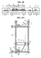
- FIG. 5A is a layout of a thin film transistor (TFT) substrate fabricated using a method for fabricating a TFT substrate according to an embodiment of the present invention
- FIG. 5B is a cross-sectional view taken along a line B-B′ of FIG. 5A ;
- FIGS. 6A , 7 A, 8 A, and 9 A are layouts sequentially illustrating a method for fabricating a TFT substrate according to an embodiment of the present invention
- FIGS. 6B , 7 B, 8 B, and 9 B are cross-sectional views taken along lines B-B′ of FIGS. 6A , 7 A, 8 A, and 9 A;
- FIG. 10A is a layout illustrating a TFT substrate fabricated using a method for fabricating a TFT substrate according to another embodiment of the present invention.
- FIG. 10B is a cross-sectional view taken along a line B-B′ of FIG. 10A ;
- FIGS. 11A , 13 A, and 19 A are layouts sequentially illustrating a method for fabricating a TFT substrate according to another embodiment of the present invention.
- FIGS. 11B and 12 are cross-sectional views illustrating processing steps taken along a line B-B′ of FIG. 11A ;
- FIGS. 13B through 18 are cross-sectional views illustrating processing steps taken along a line B-B′ of FIG. 13A ;
- FIG. 19B is a cross-sectional view taken along a line B-B′ of FIG. 19A .
- FIGS. 1 through 3 are cross-sectional views illustrating processing steps of a method for fabricating a metal wire according to an embodiment of the present invention.
- a conductive layer 2 a (hereinafter, referred to as a lower conductive oxide layer) formed of a conductive oxide material such as indium tin oxide (ITO) or indium zinc oxide (IZO), a conductive layer 2 b (hereinafter, referred to as an Ag conductive layer) including Ag or an Ag-alloy, and a conductive layer 2 c (hereinafter, referred to as an upper conductive oxide layer) formed of a conductive oxide material such as ITO or IZO are sequentially deposited on a substrate 1 , thereby forming a triple-layered structure 2 .
- the substrate 1 may be, for example, an insulating substrate made of glass or a semiconductor substrate made of intrinsic amorphous silicon, or doped amorphous silicon.
- the lower conductive oxide layer 2 a , the Ag conductive layer 2 b , and the upper conductive oxide layer 2 c are formed by, for example, sputtering.
- sputtering the sputtering method for forming the triple-layered structure 2 using ITO and Ag as targets for sputtering will be described.
- the lower conductive oxide layer 2 a is formed of ITO on the substrate 1 by applying power only to the ITO target without applying power to the Ag target.
- the lower conductive oxide layer 2 a is formed to a thickness of about 30-300 ⁇ .
- the thickness of the lower conductive oxide layer 2 a is greater than 30 ⁇ , sufficient adhesion can be secured between the substrate 1 and the Ag conductive layer 2 b by effectively preventing the substrate 1 and the Ag conductive layer 2 b from partially contacting each other.
- the thickness of the lower conductive oxide layer 2 a be less than 300 ⁇ to achieve a desirable contact resistance. More preferably, the lower conductive oxide layer 2 a is formed to a thickness of 50-100 ⁇ .
- Sputtering may be performed, for example, at a temperature of about 150 ⁇ or less, preferably, at room temperature. At such temperature, a conductive oxide material including ITO cannot be crystallized, i.e., can take an amorphous form. When ITO is deposited under such a condition, amorphous ITO is formed. At this time, hydrogen gas (H 2 ) or steam (H 2 O) may be supplied.
- ITO nitride (ITON) may be formed by exposing ITO to a nitrogen supply gas such as nitrogen gas (N 2 ), ammonia (NH 3 ), or nitrous oxide (N 2 O). ITO nitride (ITON) suppresses a sharp increase of wire resistance by preventing oxidation of Ag in a contact area between Ag and ITO.
- the Ag conductive layer 2 b is formed to a thickness of about 1000-3000 ⁇ , preferably 1500-2000 ⁇ .
- the lower conductive oxide layer 2 a formed of amorphous ITO is interposed between the Ag conductive layer 2 b and the substrate 1 .
- Amorphous ITO is a material with large surface roughness and includes a lot of concave and convex portions on its surface. With the concave and convex portions, contact areas between the substrate 1 and the lower conductive oxide layer 2 a and between the lower conductive oxide layer 2 a and the Ag conductive layer 2 b increase, thereby improving adhesion.
- the upper conductive oxide layer 2 c is formed of amorphous ITO, adhesion between a layer to be formed on the triple-layered structure 2 , e.g., an insulating layer, and the Ag conductive layer 2 b increases.
- the upper conductive oxide layer 2 c also prevents Ag from diffusing from the Ag conductive layer 2 b to the upper direction of the triple-layered structure 2 .
- the upper conductive oxide layer 2 c may be formed to a thickness of about 30-300 ⁇ , preferably 50-100 ⁇ , like the lower conductive oxide layer 2 a.
- a photoresist layer is coated on the triple-layered structure 2 and is then exposed and developed, thereby forming a photoresist pattern 3 that defines a wire pattern.
- the triple-layered structure 2 is etched using the photoresist pattern 3 as an etching mask and the photoresist pattern 3 is then removed, thereby forming the triple-layered wire 2 .
- the etching with respect to the triple-layered structure 2 may be wet etching using an etchant.
- the etchant according to an embodiment of the present invention used for wet etching, includes a material having the formula 1, ammonium acetic acid, and the remainder of deionized water, wherein the formula 1 is expressed by: M(OH) X L Y (1) where M indicates Zn, Sn, Cr, Al, Ba, Fe, Ti, Si, or B, X indicates 2 or 3, L indicates H 2 O, NH 3 , CN, COR, or NH 2 R, Y indicates 0, 1, 2, or 3, and R indicates an alkyl group.
- the material represented by Formula 1 functions as a stabilizer that enhances the stability of the etchant and improves the profile of the etched material by increasing etching uniformity.
- An amount of the material contained in the etchant may be, for example, 0.1-5 wt % with respect to the total amount of the etchant.
- An amount of the material in the etchant greater than 0.1 wt % gives the desired uniformity with the understanding that the desired etching uniformity and etchant stability is achieved for an amount of the material in the etchant up to 5 wt %. It is preferable that the amount of the material in the etchant be between 0.5-2 wt %.
- Ammonium acetic acid is used in a trivial amount in the etchant together with the material represented by Formula 1 to improve both etching uniformity and the resulting etched profile.
- the amount of ammonium acetic acid may be, for example, within a range of 0.001-0.1 wt % with respect to the total amount of the etchant. While ammonium acetic acid in the etchant within this range gives the desired improvement in etch uniformity and etching profile, it is preferable that the amount of ammonium acetic acid be in a range of 0.002-0.005 wt %.
- the amount of the material represented by Formula 1 and the amount of ammonium acetic acid are not limited to the ranges stated above, but may vary with the etching target, etching temperature, etching time, etching method, and the type of additive, all of which fall within the scope of the present invention.
- the etchant according to an embodiment of the present invention may further include phosphoric acid, nitric acid, and acetic acid.
- phosphoric acid increases etching speed.
- the amount of phosphoric acid may be in a range of 50-80 wt % with respect to a total amount of the etchant. When the amount of phosphoric acid is greater than 50 wt %, sufficiently high etching speed can be secured. When the amount of phosphoric acid is greater than 80 wt %, a difficulty in spraying the etchant due to an increase in viscosity is observed. This difficulty can be avoided by limiting the amount of phosphoric acid to less than 80 wt %. It is preferable that the amount of phosphoric acid be in a range of 60-70 wt %.
- Nitric acid improves etching speed.
- the amount of nitric acid may be in a range of 0.1-10 wt % with respect to the total amount of the etchant. When the amount of nitric acid is greater than 0.1 wt %, etching speed sufficiently increases. When the amount of phosphoric acid is greater than 10 wt %, it is possible to damage a photoresist layer. Phosphoric acid less than 10 wt % in the etchant effectively prevents damage to the photoresist layer. It is preferable that the amount of nitric acid be in a range of 0.5-5 wt %.
- Acetic acid improves wettability with respect to a photoresist layer.
- the amount of acetic acid may be in a range of 1-25 wt %.
- the amount of acetic acid is greater than 1 wt %, it is possible to effectively prevent etching from being performed incompletely due to degradation in wettability of the etchant with respect to the photoresist layer.
- the amount of acetic acid is less than 25 wt %, it is possible to prevent the life span of the etchant from being shortened due to a significant change in composition of the etchant, by suppressing evaporation of acetic acid. It is preferable that the amount of acetic acid be in a range of 2-10 wt %.
- an additive such as a surfactant may be further included in the etchant.
- the surfactant may be an anionic surfactant, a cationic surfactant, or a non-ion surfactant.
- the amount of the surfactant contained in the etchant may be in a range of 0.001-1 wt %, preferably 0.005-0.1 wt %.
- the remainder of the etchant may include deionized water in addition to the material.
- the etchant may be fabricated by, but not limited to, mixing the material represented by Formula 1, ammonium acetic acid, phosphoric acid, nitric acid, and acetic acid in deionized water or by mixing a previously fabricated solution of materials in ultra-super water. In addition, there is no specific limit in the mixing order.
- microspheres in the etchant When there are microspheres in the etchant, fine patterns may not be properly etched. Thus, before the etchant is used it is desirable to remove the microspheres from the etchant so that the number of microspheres with a diameter of 0.5 ⁇ m or more can be less than 1000/mL.
- the microspheres may be removed by filtering the etchant using a fine filter.
- the filtering may be one-time filtering, preferably circulating filtering in which microspheres are removed at high speeds.
- the etchant has a high etch selectivity to the triple-layered structure 2 , maintains adhesion of the triple-layered structure 2 to the substrate 1 , and allows the side profile of the triple layer wire 2 to have a good tapered acute angle.
- Etching of the triple-layered structure 2 may be individually performed on each of the upper conductive oxide layer 2 c , the Ag conductive layer 2 b , and the lower conductive oxide layer 2 a .
- ITO included in the upper conductive oxide layer 2 c and the lower conductive oxide layer 2 a and Ag or an Ag-alloy included in the Ag conductive layer 2 b have a similar etching speed
- the upper conductive oxide layer 2 c , the Ag conductive layer 2 b , and the lower conductive oxide layer 2 a may be etched in a batch manner, leading to a good side profile of the triple-layered wire 2 .
- Etching may be performed by spraying the etchant onto the surface of the triple-layered structure 2 in which the photoresist pattern 3 is formed.
- an etching temperature may be maintained at about 30-50° C.
- An etching time may last until a half of the time detected by an end point detector (EPD) during which the substrate 1 is exposed to the etchant additionally passes.
- the etching time may be about 30-100 seconds.
- FIG. 4 is a cross-sectional picture illustrating a profile of a metal wire after a triple-layered wire including ITO, an Ag conductive layer, and ITO formed on a substrate is patterned using the etchant according to an embodiment of the present invention.
- the Ag conductive layer 2 b included in the triple-layered structure 2 has poor adhesion to the substrate 1 .
- the lower conductive oxide layer 2 a and the upper conductive oxide layer 2 c formed of ITO, are formed under and on the Ag conductive layer 2 b .
- adhesion of the triple-layered structure 2 to the substrate 1 is degraded as the etching process progresses, causing lifting or peeling of the triple-layered wire 2 .
- the side profile of the triple-layered wire 2 is not uniform and may have inverse taper tilt angle.
- a triple-layered structure including a lower conductive oxide layer, an Ag conductive layer, and an upper conductive oxide layer on a substrate is taken as an example in this embodiment of the present invention, a multi-layered conductive layer may be formed which is equivalent to the conductive oxide layer either under or on the Ag conductive layer.
- the etchant and the method for fabricating an Ag wire using the etchant may also be applied to a method for fabricating a thin film transistor (TFT) substrate.
- TFT thin film transistor
- FIG. 5A is a layout of a thin film transistor (TFT) substrate fabricated using a method for fabricating a TFT substrate according to an embodiment of the present invention
- FIG. 5B is a cross-sectional view taken along a line B-B′ of FIG. 5A .
- TFT thin film transistor
- a plurality of gate wires transmitting a gate signal are formed on an insulating substrate 10 ( FIG. 5B ).
- the gate wires include a gate line 22 shown as horizontally extending in FIG. 5A , a gate end 24 that is connected to the end of the gate line 22 to receive a gate signal from the outside and transmit the same to the gate line 22 , a gate electrode 26 of a protruding TFT that is connected to the gate line 22 , and a sustain electrode 27 and a sustain electrode line 28 formed parallel with the gate line 22 .
- the sustain electrode line 28 horizontally extends across a pixel region and is connected to the sustain electrode 27 that is wider than the sustain electrode line 28 .
- the sustain electrode 27 overlaps with, but is separted by dielectric 30 (not shown in FIG.
- a drain electrode extension portion 67 connected with a pixel electrode 82 to form a sustain electric condenser that improves electric charge retention capability of a pixel.
- the shapes and arrangements of the sustain electrode 27 and the sustain electrode line 28 may vary, and the sustain electrode 27 and the sustain electrode line 28 may not be formed if it is determined that the sustain capability generated by the overlap between the pixel electrode 82 and the gate line 22 is sufficiently high.
- the gate wires are formed of triple layers 22 , 24 , 26 , 27 , and 28 .
- the triple-layered gate line 22 includes conductive layers 221 , 222 , and 223 .
- the triple layer 24 includes conductive layers 241 , 242 , and 243 .
- the triple layer 26 includes conductive layers 261 , 262 , and 263 .
- the triple layer 27 includes conductive layers 271 , 272 , and 273 .
- the conductive layers 221 , 241 , 261 , and 271 are formed of a conductive oxide material such as indium tin oxide (ITO) or indium zinc oxide (IZO) (hereinafter, referred to as “lower conductive oxide layers”).
- ITO indium tin oxide
- IZO indium zinc oxide
- the conductive layers 222 , 242 , 262 , and 272 are formed of Ag or an Ag-alloy.
- the conductive layers 223 , 243 , 263 , and 273 are formed of a conductive oxide material such as ITO or IZO (hereinafter, referred to as “upper conductive oxide layers”).
- the sustain electrode line 28 also has the same triple layer structure as the triple layers 22 , 24 , 26 , and 27 .
- the following description of the gate wires having the triple layer structures includes the sustain electrode line 28 .
- triple layers 22 , 24 , 26 , 27 , and 28 are the same as those of the above-described triple layers in the method for fabricating an Ag wire according to an embodiment of the present invention.
- a gate insulating layer 30 is formed of silicon nitride (SiNx) on the substrate 10 and the triple layers 22 , 24 , 26 , 27 , and 28 .
- a semiconductor layer 40 is formed of amorphous silicon hydride or polycrystalline silicon in the shape of an island on the gate insulating layer 30 on the gate electrode 26 .
- Resistive contact layers 55 and 56 are formed of silicide or n+ amorphous silicon hydride in which an n-type impurity is highly doped, on the semiconductor layer 40 .
- Data wires are formed on the resistive contact layers 55 and 56 and the gate insulating layer 30 .
- the data wires include a data line 62 that is shown formed vertically in FIG. 5A and intersects the gate line 22 to define a pixel, a source electrode 65 that is a branch of the data line 62 and extends onto the resistive contact layer 55 , a data end 68 that is connected to an end of the data line 62 and receives an image signal from the outside, a drain electrode 66 that is separated from the source electrode 65 and is formed on the resistive contact layer 56 opposite to the source electrode 65 in view of the gate electrode 26 or a channel portion of a TFT, and a drain electrode extension portion 67 with a large area that extends from the drain electrode 66 and overlaps with, but is separated by dielectric 30 from, the sustain electrode 27 .
- the data wires are formed of the triple layers 62 , 65 , 66 , 67 , and 68 .
- the triple-layered data line 62 includes conductive layers 621 , 622 , and 623 .
- the triple-layered source electrode 65 includes conductive layers 651 , 652 , and 653 .
- the triple-layered drain electrode 66 includes conductive layers 661 , 662 , and 663 .
- the triple layer 67 includes conductive layers 671 , 672 , and 673 .
- the triple layer 68 includes conductive layers 681 , 682 , and 683 .
- the conductive layers 621 , 651 , 661 , 671 , and 681 are formed of a conductive oxide material such as ITO (hereinafter, referred to as “lower conductive oxide layers”).
- the conductive layers 622 , 652 , 662 , 672 , and 682 are formed of Ag or an Ag-alloy (hereinafter, referred to as “Ag conductive layers”).
- the conductive layers 623 , 653 , 663 , 673 , and 683 are formed of a conductive oxide material such as ITO (hereinafter, referred to as “upper conductive oxide layers”).
- the source electrode 65 has at least a portion that overlaps with the semiconductor layer 40 .
- the drain electrode 66 is located opposite the source electrode and as shown in FIG. 5B above a portion of the gate electrode 26 and has at least a portion that overlaps a portion of the semiconductor layer 40 .
- the resistive layers 55 and 56 exist between the semiconductor layer 40 and the source electrode 65 and between the semiconductor layer 40 and the drain electrode 66 , respectively, to reduce contact resistances therebetween.
- the drain electrode extension portion 67 overlaps the sustain electrode 27 to form sustain capability (i.e. the ability of the capacitor formed by drain electrode extension portion 67 , gate insulating layer 30 and sustain electrode 27 to hold a charge) between the sustain electrode 27 and the gate insulating layer 30 on the one hand, and drain electrode extension portion 67 , on the other hand.
- sustain capability i.e. the ability of the capacitor formed by drain electrode extension portion 67 , gate insulating layer 30 and sustain electrode 27 to hold a charge
- the drain electrode extension portion 67 is not formed either.
- a passivation layer 70 is formed on the data wires and portions of the semiconductor layer 40 that are not covered by the data wires.
- the passivation layer 70 may be formed of, for example, an organic material having superior planarization properties and photosensitivity, an insulating material having a low dielectric constant formed by plasma enhanced chemical vapor deposition (PECVD), such as a-Si:C:O or a-Si:O:F, or an inorganic material such as SiNx.
- PECVD plasma enhanced chemical vapor deposition
- an insulating layer (not shown) formed of silicon nitride (SiNx) or silicon oxide (SiOx) or silicon dioxide (SiO 2 ) may be further formed under the passivation layer 70 to prevent the organic material of the passivation layer 70 from contacting a portion of the semiconductor layer 40 between the source electrode 65 and the drain electrode 66 .
- Contact holes 77 and 78 that expose the drain electrode extension portion 67 and the data line end 68 are formed in the passivation layer 70 .
- a contact hole 74 that exposes the gate line end 24 is formed in the passivation layer 70 and the gate insulating layer 30 .
- a pixel electrode 82 that is electrically connected to the drain electrode 66 through the contact hole 77 and is located in a pixel is formed on the passivation layer 70 .
- the pixel electrode 82 to which a data voltage is applied determines the arrangement of liquid crystal (“LC”) microspheres of a liquid crystal layer between the pixel electrode 82 and a common electrode of an upper display panel (not shown) by generating an electric field with the common electrode.
- LC liquid crystal
- auxiliary gate end 84 connected to the gate end 24 through the contact hole 74 and an auxiliary data end 88 connected to the data end 68 through the contact hole 78 are formed on the passivation layer 70 .
- the pixel electrode 82 , the auxiliary gate end 84 , and the auxiliary data end 88 are formed of ITO.
- FIGS. 5A and 5B and FIGS. 6A through 9B a method for fabricating a TFT substrate according to an embodiment of the present invention will be described in detail with reference to FIGS. 5A and 5B and FIGS. 6A through 9B .
- a conductive layer formed of a conductive oxide material such as ITO or IZO, a conductive layer formed of Ag, and a conductive layer formed of a conductive oxide material such as ITO or IZO are sequentially deposited on the insulating substrate 10 , thereby forming the gate triple-layers 22 , 24 , 26 , 27 , and 28 (not shown in FIG. 6B ) including the lower conductive oxide layers 221 , 241 , 261 , and 271 , the conductive layers 222 , 242 , 262 , and 272 , and the upper conductive oxide layers 223 , 243 , 263 , and 273 .
- the gate triple-layers 22 , 24 , 26 , 27 , and 28 are formed by a method of forming the triple layers in the method for fabricating an Ag wire according to an embodiment of the present invention.
- photolithography is performed on the gate triple-layers.
- the photolithography process is performed by wet etching using an etchant.
- the etchant is the same as that described with reference to FIGS. 1 through 4 ; therefore an explanation thereof will not be given.
- the etchant has a high etch selectivity to triple layers and demonstrates superior etching uniformity, a side profile having good tapered acute angle can be obtained without affecting adhesion of the triple-layered gate wires 22 , 24 , 26 , 27 , and 28 to the substrate 10 .
- the gate wires including the gate line 22 , the gate electrode 26 , the gate end 24 , the sustain electrode 27 , and the sustain electrode line 28 are formed.
- the gate insulating layer 30 (sometimes referred to herein as dielectric 30 ) formed of silicon nitride, an intrinsic amorphous silicon layer (to become silicon layer 40 ), and a doped amorphous silicon layer (to become resistive contacts 55 and 56 ) are continuously deposited to thicknesses of 1500-5000 ⁇ , 500-2000 ⁇ , and 300-600 ⁇ , using, for example, chemical vapor deposition (CVD). Photolithography is performed on the intrinsic amorphous silicon layer 40 and the doped amorphous silicon layer to form the semiconductor layer 40 taking the shape of an island and to form the resistive contact layers 55 and 56 on the gate insulating layer 30 overlying the gate electrode 24 .
- CVD chemical vapor deposition
- the gate insulating layer 30 , the intrinsic amorphous silicon layer 40 , and the doped amorphous silicon layer are formed at a high temperature of about 200 ⁇ or more, amorphous ITO included in the gate wires changes into crystalline ITO.
- adhesion between the conductive oxide layers 221 , 241 , 261 , 271 , 223 , 243 , 263 , and 273 and the Ag conductive layers 222 , 242 , 262 , and 272 is improved.
- Photolithography is performed on the data triple layers.
- the photolithography process is performed by wet etching using an etchant.
- the etchant is the same as that described with reference to FIGS. 1 through 4 ; thus a further explanation thereof will not be given.
- the etchant has a high etch selectivity to the data triple layers and demonstrates superior etching uniformity, a side profile having good tapered acute angle can be obtained without affecting adhesion of the triple-layered data wires 62 , 65 , 66 , 67 , and 68 to the gate insulating layer 30 and the resistive contact layers 55 and 56 .
- the data wires 62 , 65 , 66 , 67 , and 68 are formed, which include the data line 62 that intersects the gate line 22 , the source electrode 65 that is connected to the data line 62 and extends onto the gate electrode 26 , the data end 68 that is connected to an end of the data line 62 , the drain electrode 66 that is separated from the source electrode 65 and is located in opposition to the source electrode 65 in view of the gate electrode 26 , and the drain electrode extension protrusion 67 with a large area that extends from the drain electrode 66 and overlaps with, but is separated by dielectric 30 from, the sustain, electrode 27 .
- the data wires 62 , 65 , 66 , 67 , and 68 are separated but portions 65 and 66 thereof remain over both sides of the gate electrode 26 as shown in FIG. 5B by etching away portions of the doped amorphous silicon layer that are not covered by the data wires to, among other things, expose a portion of the semiconductor layer 40 between the resistive contact layers 55 and 56 . At this time, it is desirable to perform oxygen plasma processing to stabilize the surface of the exposed portion of the semiconductor layer 40 .
- the passivation layer 70 is formed as a single layer or multiple layers including an organic material having superior planarization properties and photosensitivity.
- passivation layer 70 can be formed of a-Si:C:O formed by PECVD, an insulating material having a low dielectric constant, such as a-Si:O:F, or an inorganic material such as SiNx.
- the gate insulating layer 30 and the passivation layer 70 are patterned by photolithography, thereby forming the contact holes 74 , 77 , and 78 that expose the gate end 24 , the drain electrode extension protrusion 67 , and the data end 68 .
- the contact holes 74 , 77 , and 78 may be formed only by photolithography. It is desirable to form the contact holes 74 , 77 , and 78 using an etchant and an etch process which has the same selectivity to the gate insulating layer 30 and the passivation layer 70 .
- an ITO layer is deposited and photolithography is performed to form the pixel electrode 82 connected to the drain electrode 66 through the contact hole 77 , form the auxiliary gate end 84 connected to the gate end 24 through the contact hole 74 , and form the auxiliary data end 88 connected to the data end 68 through the contact hole 78 .
- a gate wire and a data wire are formed of a triple-layer structure including a lower conductive oxide layer, an Ag conductive layer, and an upper conductive oxide layer on a substrate in this embodiment of the present invention, only the gate wire or the data wire may be formed by a triple-layered structure.
- the conductive oxide layer may be a multi-layered conductive layer formed either under or on the Ag conductive layer.
- a semiconductor layer and a data wire are formed through photolithography using different masks in the above description, but they can also be formed through photolithography using a single photoresist pattern as in the following description.
- FIGS. 10A through 19B The structure of a unit pixel of a TFT substrate fabricated by a method for fabricating a TFT substrate according to another embodiment of the present invention will be described with reference to FIGS. 10A through 19B .
- FIG. 10A is a layout illustrating a TFT substrate fabricated using a method for fabricating a TFT substrate according to another embodiment of the present invention
- FIG. 10B is a cross-sectional view taken along a line B-B′ of FIG. 10A .
- a plurality of gate wires transmitting a gate signal are first formed on an insulating substrate 10 .
- the gate wires include a gate line 22 that extends horizontally, as shown in FIG. 10A , a gate end 24 that is connected to the end of the gate line 22 to receive a gate signal from the outside and transmit the same to the gate line 22 , a gate electrode 26 of a protruding TFT that is connected to the gate line 22 , and a sustain electrode 27 and a sustain electrode line 28 formed parallel with the gate line 22 .
- the sustain electrode line 28 extends horizontally in FIG. 10A across a pixel region and is connected to the sustain electrode 27 that is wider than the sustain electrode line 28 .
- the sustain electrode 27 as shown in FIG.
- the shapes and arrangements of the sustain electrode 27 and the sustain electrode line 28 may vary, and the sustain electrode 27 and the sustain electrode line 28 may not be formed when sustain capability generated by the overlap between the pixel electrode 82 and the gate line 22 is sufficiently high.
- the gate wires 22 , 24 , 26 , 27 , and 28 are formed of triple layers including the lower conductive oxide layers 221 , 241 , 261 , and 271 formed of ITO or IZO, the conductive layers 222 , 242 , 262 , and 272 formed of Ag or an Ag-alloy, and the upper conductive oxide layers 223 , 243 , 263 , and 273 formed of ITO or IZO as in the embodiment of the present invention shown in FIGS. 5A through 9B .
- the gate insulating layer 30 is formed on the substrate 10 and the gate wires 22 , 24 , 26 , 27 , and 28 .
- Semiconductor patterns 42 , 44 , and 48 are formed on the gate insulating layer 30 .
- Resistive contact layers 52 , 55 , 56 , and 58 are formed on the semiconductor patterns 42 , 44 , and 48 .
- the data wires 62 , 65 , 66 , 67 , and 68 are formed on the resistive contact layers 52 , 55 , 56 , and 58 .
- the data wires include a data line 62 that is shown vertically in FIG. 10A and intersects the gate line 22 to define a pixel, a source electrode 65 that is a branch of the data line 62 and extends onto the resistive contact layer 55 a data end 68 that is connected to an end of the data line 62 and receives an image signal from the outside, a drain electrode 66 that is separated from the source electrode 65 and is formed on the resistive contact layer 56 opposite to the source electrode 65 in view of (i.e. to overlie a portion of) the gate electrode 26 which defines a channel portion of a TFT, and a drain electrode extension portion 67 with a large area that extends from the drain electrode 66 and overlaps with the sustain electrode 27 .
- the data wires 62 , 65 , 66 , 67 , and 68 are formed of triple layers including the conductive layers 621 , 651 , 661 , 671 , and 681 formed of a conductive oxide material (hereinafter, referred to as “lower conductive oxide layers”), the conductive layers 622 , 652 , 662 , 672 , and 682 formed of Ag or an Ag-alloy (hereinafter, referred to as “Ag conductive layers”), and the conductive layers 623 , 653 , 663 , 673 , and 683 formed of a conductive oxide material (hereinafter, referred to as “upper conductive oxide layers”).
- the source electrode 65 has at least a portion that overlaps with a portion of layer 44 (formed by an earlier photolithographic step involving patterning and etching the semiconductor layer 40 ) and the drain electrode 66 is located in opposition to the source electrode 65 in view of (i.e. so as to overlie a portion of) the gate electrode 26 and has at least a portion that overlaps with a portion of semiconductor layer 44 .
- the resistive layers 55 and 56 exist between the semiconductor layer 44 and the source electrode 65 and between the semiconductor layer 44 and the drain electrode 66 , respectively, to reduce contact resistances therebetween.
- the drain electrode extension portion 67 overlaps with the sustain electrode 27 to form sustain capability between the sustain electrode 27 with the gate insulating layer 30 seerving as a dielectric between electrodes 27 and 67 .
- the drain electrode extension portion 67 is not formed either.
- the resistive contact layers 52 , 55 , 56 , and 58 reduce contact resistances between the semiconductor patterns 42 , 44 , and 48 and the data wires 62 , 65 , 66 , 67 , and 68 and have the same shapes in plan view as the data wires 62 , 65 , 66 , 67 , and 68 .
- the semiconductor patterns 42 , 44 , and 48 have the same shapes as those of the data wires 62 , 65 , 66 , 67 , and 68 and the resistive contact layers 52 , 55 , 56 , and 58 except for a channel portion of a TFT.
- the source electrode 65 and the drain electrode 66 are separated and the resistive contact layer 55 under the source electrode 65 and the resistive contact layer 56 under the drain electrode 66 are separated.
- the semiconductor pattern 44 for the TFT is continuous in the channel portion of the TFT, thereby forming a channel of the TFT.
- the passivation layer 70 is formed on the data wires 62 , 65 , 66 , 67 , and 68 and a portion of the semiconductor pattern 44 that is not covered by the data wires 62 , 65 , 66 , 67 , and 68 .
- the passivation layer 70 may be formed of, for example, an organic material having superior planarization properties and photosensitivity, an insulating material having a low dielectric constant formed by plasma enhanced chemical vapor deposition (PECVD), such as a-Si:C:O or a-Si:O:F, or an inorganic material such as SiNx.
- PECVD plasma enhanced chemical vapor deposition
- an insulating layer (not shown) formed of silicon nitride (SiNx) or silicon oxide (SiOx) or silicon dioxide (SiO 2 ) may be further formed under the passivation layer 70 to prevent the organic material of the passivation layer 70 from contacting a portion of the semiconductor layer 40 between the source electrode 65 and the drain electrode 66 .
- a pixel electrode 82 that is electrically connected to the drain electrode 66 through the contact hole 77 and is located in a pixel is formed on the passivation layer 70 .
- a data voltage applied to the pixel electrode 82 determines the arrangement of LC microspheres of a liquid crystal layer between the pixel electrode 82 and a common electrode of an upper display panel (not shown) by generating an electric field with the common electrode.
- an auxiliary gate end 84 connected to the gate end 24 through the contact hole 74 and an auxiliary data end 88 connected to the data end 68 through the contact hole 78 are formed on the passivation layer 70 .
- the pixel electrode 82 , the auxiliary gate end 84 , and the auxiliary data end 88 are formed of ITO.
- FIGS. 10A and 10B and FIGS. 11A through 19B a method for fabricating a TFT substrate according to another embodiment of the present invention will be described with reference to FIGS. 10A and 10B and FIGS. 11A through 19B .
- the gate triple layers 22 , 24 , 26 , 27 , and 28 are formed by sequentially depositing the lower conductive oxide layers 221 , 241 , 261 , and 271 formed of a conductive oxide material such as ITO or IZO, the conductive layers 222 , 242 , 262 , and 272 formed of Ag, and the upper conductive oxide layers 223 , 243 , 263 , and 273 formed of a conductive oxide material such as ITO or IZO as in the embodiment of the present invention shown in FIGS. 5A through 9B .
- a conductive oxide material such as ITO or IZO
- photolithography is performed on the gate triple layers 22 , 24 , 26 , 27 , and 28 .
- the photolithography process is performed by wet etching using an etchant.
- the etchant is the same as that described with reference to FIGS. 1 through 4 and an explanation thereof will not be given.
- the gate wires including the gate line 22 , the gate electrode 26 , the gate end 24 , the sustain electrode 27 , and the sustain electrode line 28 are formed.
- the gate insulating layer 30 formed of silicon nitride, an intrinsic amorphous silicon layer 40 , and a doped amorphous silicon layer 50 are continuously deposited to thicknesses of, for example, 1500-5000 ⁇ , 500-2000 ⁇ , and 300-600 ⁇ , respectively, using CVD.
- a data triple layer 60 in which a lower conductive oxide layer 601 formed of ITO, an Ag conductive layer 602 formed of Ag or an Ag-alloy, and an upper conductive oxide layer 603 formed of ITO are sequentially stacked is then formed on the doped amorphous silicon layer 50 using sputtering.
- a deposition method for the data triple layer 60 is the same as that for the data triple layer in the embodiment of the present invention shown in FIGS. 5A through 9B .
- a photoresist layer 110 is coated onto the data triple layer 60 .
- FIGS. 13A through 18 light is projected onto the photoresist layer 110 through a mask and development is performed. Thus, photoresist patterns 112 and 114 as shown in FIG. 13B are formed. At this time, in the photoresist patterns 112 and 114 , a channel portion of the to-be-formed TFT, i.e., a first portion of amorphous silicon layer 40 beneath photoresist 114 ( FIG. 13B ) and between the to-be-formed source electrode 65 and the to-be-formed drain electrode 66 ( FIGS.
- photoresist 114 which has a thickness that is smaller than that of the photoresist 112 over the data wire portion, i.e., a second portion of photoresist 112 that is located over a region in which a data wire is to be formed.
- the remaining portions of photoresist layer 110 ( FIG. 12 ) except for the channel portion of photoresist 114 and the data wire portions of photoresist 112 are removed.
- the ratio of the thickness of the photoresist layer 114 remaining above the channel portion of the to-be-formed TFT transistor to the thickness of the photoresist layer 112 remaining over the data wire portions varies as a function of the etching process to be described later.
- the thickness of the first photoresist portion 114 be smaller than 1 ⁇ 2 of the thickness (approximately 8000 ⁇ in one embodiment) of the second photoresist portion 112 , e.g., smaller than 4000 ⁇ .
- the thickness of the photoresist layer 110 may vary with position in various ways. One way is to use well-known photolithographic techniques to vary the amount of light incident on various portions of photoresist layer 110 . To adjust the amount of transmitted light, a slit or a lattice pattern is formed or a semi-transparent film is used as part of the mask used to pattern the photoresist layer 110 .
- the line width of a pattern between slits on a mask or an interval between patterns on a mask i.e., the width of a slit, be smaller than the resolution of an exposure system.
- a semi-transparent layer is used as a mask
- a thin film having a transmissivity or thickness that is different from that of the semi-transparent layer may be used as part of the mask to control transmissivity of portions of the mask at the time of fabricating a mask.
- Photoresist portion 114 is a portion to which a little light is projected.
- the polymer material may be novolac resin and the exposure time, expressed as an energy, may be about 36 mmJ
- the photoresist portion 114 having a smaller thickness than the photoresist portions 112 is formed by exposing a photoresist layer formed of a material capable of reflowing through a general mask divided into a portion the light can completely penetrate and a portion the light cannot penetrate at all, developing the photoresist layer, and making the photoresist layer reflow such that a portion of the photoresist layer 114 flows to a region where the photoresist layer 114 does not remain.
- the “reflow process” may be performed by heating the photoresist layer over the photoresist transition temperature and flowing the photoresist layer down to the channel portion.
- the photoresist pattern 114 and the data triple layer 60 including the upper conductive oxide layer 603 , the Ag conductive layer 602 , and the lower conductive oxide layer 601 are now etched using the etchant described above. Since the etching is substantially the same as the etching for, forming the data wires and the etching for forming the gate wires 22 , 24 , 26 , 28 , and 29 in the embodiment of the present invention shown in FIGS. 5A through 9B , an explanation thereof will not be given.
- triple-layered patterns 64 of the to-be-formed channel portion and 62 , and 68 of the data line portions remain.
- the other portions of the data triple layer 60 are entirely removed.
- the doped amorphous silicon layer 50 is exposed.
- the remaining triple-layered patterns 62 , 64 and 68 are the same as the data wires ( 62 , 65 , 66 , 67 , and 68 of FIG. 5B ) except that the source electrode 65 and the drain electrode 66 are not yet separated (i.e. defined) in FIGS. 14 and 15 .
- the exposed, doped amorphous silicon layer 50 and the intrinsic amorphous silicon layer 40 are dry etched to remove all portions of these layers except for the channel portion (layer 44 in FIG. 15 ) and the data wire portions (layers 42 and 48 in FIG. 15 ).
- the first portion 114 of the photoresist layer is also removed by this dry etching.
- the result of this dry etching is shown in cross-sectional view in FIG. 15 . This etching preferably is performed such that the photoresist patterns 112 and 114 , the doped amorphous silicon layer 50 , and the intrinsic amorphous silicon layer 40 are etched simultaneously but the gate insulating layer 30 is not etched.
- etching be performed on condition that the etch selectivities to the photoresist patterns 112 and 114 and the intrinsic amorphous silicon layer 40 are similar to each other.
- two layers may be etched to similar thicknesses by using a mixed gas of SF 6 or HCl or a mixed gas of SF 6 or O 2 .
- the thickness of the first portion 114 is equal to or smaller than a total thickness of the intrinsic amorphous silicon layer 40 and the doped amorphous silicon layer 50 .
- the dry etching is stopped at the appropriate time such that the dielectric layer 30 and the ITO layer 643 are not substantially etched by this dry etching step.
- the mixed gas containing, for example, SF6 and HCL is passed into the reaction chamber and a high frequency field is applied to the reaction chamber to induce glow discharge plasma. Dry etching is performed by colliding this plasma with the intrinsic amorphous silicon layer and the doped amorphous silicon layer.
- a source/drain triple-layered pattern 64 is exposed after removal of the first portion 114 of the channel portion and the gate insulating layer 30 is exposed after removal of the doped amorphous silicon layer 50 and the intrinsic amorphous silicon layer 40 of the other portion. Since the second photoresist portion 112 covering the data wire portion is also etched, the thickness of photoresist portion 112 is reduced by at least the thickness of photoresist portion 114 .
- Residues of the photoresist layer 110 remaining on the surface of the source/drain triple-layered pattern 64 of the channel portion are removed through ashing.
- a portion of the triple-layered pattern 64 shown in FIG. 15 including portions of the upper conductive oxide layer 643 of the channel portion, the Ag conductive layer 642 , and the lower conductive oxide layer 641 are removed through, for example, wet etching to expose the top surface of doped amorphous silicon layer 50 .
- the same etchant as described above with reference to FIGS. 1 through 4 is used for this etching step. Therefore this etching step will not be described again.
- the resistive contact layer formed of doped amorphous silicon 50 is etched. At this time, dry etching may be used.
- the etching gas may be a mixture of CF 4 and HCl or a mixture of CF 4 and O 2 .
- CF 4 and O 2 are used, a uniform thickness of the semiconductor pattern 44 formed of intrinsic amorphous silicon can remain. At this time, a portion of the semiconductor layer 44 is removed as shown in FIG. 16 and thus, the thickness of layer 44 may be reduced where it has been etched, as shown.
- the second portion 112 of the photoresist pattern may also be etched and thus the thickness of this photoresist 112 will be reduced. Etching should be performed so that the gate insulating layer 30 is not etched.
- the photoresist pattern 112 should be thick such that the data wires 62 , 65 , 66 , 67 , and 68 are not exposed after etching of the second portion 112 .
- the source electrode 65 and the drain electrode 66 are separated and defined, thereby completing the formation of the data wires 65 and 66 which make up these electrodes along with the resistive contact layers 55 and 56 .
- the second portion 112 of the photoresist layer remaining over the data wire portion of the structure is removed.
- the passivation layer 70 is formed over the top surface of the structure. Typically this layer is formed of silicon nitride. As shown in FIGS. 19A and 19B , photolithography is performed on the passivation layer 70 and the gate insulating layer 30 , thereby forming the contact holes 77 , 74 and 78 that expose the drain electrode extension portion 67 , the gate end 24 , and the data end 68 .
- an ITO layer having a thickness of 400-500 ⁇ is deposited and undergoes photolithography, thereby forming the pixel electrode 82 connected to the drain electrode extension portion 67 , the auxiliary gate end 84 connected to the gate end 24 and the auxiliary data end 88 connected to the data end 68 .
- an effect according to the embodiment of the present invention can be obtained, and the data wires 62 , 65 , 66 , 67 , and 68 , the resistive contact layers 52 , 55 , 56 , and 58 , and the semiconductor patterns 42 and 48 are formed using a single mask, during which the source electrode 65 and the drain electrode 66 are separated and defined, thereby simplifying a fabrication process.
- the gate wire or the data wire may have a triple-layered structure.
- the conductive oxide layer may be a multi-layered conductive layer formed either under or on the Ag conductive layer.
- a method for fabricating a TFT substrate according to the present invention can be easily applied to an array on color filter (AOC) in which a TFT array is formed on a color filter.
- AOC array on color filter
Landscapes
- Engineering & Computer Science (AREA)
- Power Engineering (AREA)
- Physics & Mathematics (AREA)
- Condensed Matter Physics & Semiconductors (AREA)
- General Physics & Mathematics (AREA)
- Computer Hardware Design (AREA)
- Microelectronics & Electronic Packaging (AREA)
- Chemical & Material Sciences (AREA)
- Manufacturing & Machinery (AREA)
- General Chemical & Material Sciences (AREA)
- Chemical Kinetics & Catalysis (AREA)
- Materials Engineering (AREA)
- Mechanical Engineering (AREA)
- Metallurgy (AREA)
- Organic Chemistry (AREA)
- Thin Film Transistor (AREA)
- Liquid Crystal (AREA)
- Weting (AREA)
- ing And Chemical Polishing (AREA)
- Electrodes Of Semiconductors (AREA)
- Internal Circuitry In Semiconductor Integrated Circuit Devices (AREA)
- Devices For Indicating Variable Information By Combining Individual Elements (AREA)
Priority Applications (1)
| Application Number | Priority Date | Filing Date | Title |
|---|---|---|---|
| US12/035,316 US7955521B2 (en) | 2005-06-09 | 2008-02-21 | Etchant and method for fabricating a thin film transistor substrate including conductive wires using the etchant and the resulting structure |
Applications Claiming Priority (2)
| Application Number | Priority Date | Filing Date | Title |
|---|---|---|---|
| KR1020050049453A KR101124569B1 (ko) | 2005-06-09 | 2005-06-09 | 식각액, 이를 이용하는 배선 형성 방법 및 박막 트랜지스터기판의 제조 방법 |
| KR10-2005-0049453 | 2005-06-09 |
Related Child Applications (1)
| Application Number | Title | Priority Date | Filing Date |
|---|---|---|---|
| US12/035,316 Division US7955521B2 (en) | 2005-06-09 | 2008-02-21 | Etchant and method for fabricating a thin film transistor substrate including conductive wires using the etchant and the resulting structure |
Publications (2)
| Publication Number | Publication Date |
|---|---|
| US20060278606A1 US20060278606A1 (en) | 2006-12-14 |
| US7357878B2 true US7357878B2 (en) | 2008-04-15 |
Family
ID=37509918
Family Applications (2)
| Application Number | Title | Priority Date | Filing Date |
|---|---|---|---|
| US11/351,015 Active 2026-04-08 US7357878B2 (en) | 2005-06-09 | 2006-02-09 | Etchant, and method for fabricating a thin film transistor subtrate including conductive wires using the etchant and the resulting structure |
| US12/035,316 Active 2028-03-10 US7955521B2 (en) | 2005-06-09 | 2008-02-21 | Etchant and method for fabricating a thin film transistor substrate including conductive wires using the etchant and the resulting structure |
Family Applications After (1)
| Application Number | Title | Priority Date | Filing Date |
|---|---|---|---|
| US12/035,316 Active 2028-03-10 US7955521B2 (en) | 2005-06-09 | 2008-02-21 | Etchant and method for fabricating a thin film transistor substrate including conductive wires using the etchant and the resulting structure |
Country Status (5)
| Country | Link |
|---|---|
| US (2) | US7357878B2 (ja) |
| JP (1) | JP4988242B2 (ja) |
| KR (1) | KR101124569B1 (ja) |
| CN (1) | CN1877448A (ja) |
| TW (1) | TWI388062B (ja) |
Cited By (7)
| Publication number | Priority date | Publication date | Assignee | Title |
|---|---|---|---|---|
| US20060205125A1 (en) * | 2005-03-09 | 2006-09-14 | Yang-Ho Bae | TFT substrate and display device having the same |
| US20090227075A1 (en) * | 2008-03-05 | 2009-09-10 | Bong-Kyun Kim | Etchant composition, patterning conductive layer and manufacturing flat panel, display device using the same |
| US20140070181A1 (en) * | 2012-02-27 | 2014-03-13 | Boe Technology Group Co., Ltd. | Array substrate, method for manufacturing the same and display device |
| US10611962B2 (en) | 2018-04-23 | 2020-04-07 | Samsung Display Co., Ltd. | Etchant composition and manufacturing method of metal pattern using the same |
| US10636666B1 (en) | 2018-10-11 | 2020-04-28 | Samsung Display Co., Ltd. | Etchant and method for manufacturing display device using the same |
| US11091694B2 (en) | 2018-11-14 | 2021-08-17 | Samsung Display Co., Ltd. | Etching composition, method for forming pattern and method for manufacturing a display device using the same |
| US11683975B2 (en) | 2020-04-29 | 2023-06-20 | Samsung Display Co., Ltd. | Etchant composition and method of manufacturing display apparatus by using the same |
Families Citing this family (19)
| Publication number | Priority date | Publication date | Assignee | Title |
|---|---|---|---|---|
| US7288444B2 (en) * | 2001-04-04 | 2007-10-30 | Samsung Sdi Co., Ltd. | Thin film transistor and method of manufacturing the same |
| KR100982395B1 (ko) * | 2007-04-25 | 2010-09-14 | 주식회사 엘지화학 | 박막 트랜지스터 및 이의 제조방법 |
| KR100987840B1 (ko) * | 2007-04-25 | 2010-10-13 | 주식회사 엘지화학 | 박막 트랜지스터 및 이의 제조방법 |
| JP2009194351A (ja) * | 2007-04-27 | 2009-08-27 | Canon Inc | 薄膜トランジスタおよびその製造方法 |
| JP5363713B2 (ja) * | 2007-07-19 | 2013-12-11 | 三洋半導体製造株式会社 | エッチング液組成物 |
| KR101747391B1 (ko) * | 2009-07-07 | 2017-06-15 | 엘지디스플레이 주식회사 | 액정표시장치용 어레이 기판 및 이의 제조 방법 |
| KR102290801B1 (ko) * | 2013-06-21 | 2021-08-17 | 가부시키가이샤 한도오따이 에네루기 켄큐쇼 | 반도체 장치 및 그 제작 방법 |
| US20150069011A1 (en) * | 2013-09-11 | 2015-03-12 | Carestream Health, Inc. | Wet etching patterning compositions and methods |
| KR102118461B1 (ko) * | 2013-11-25 | 2020-06-09 | 엘지디스플레이 주식회사 | 산화물 박막트랜지스터를 포함한 어레이기판 및 그 제조방법 |
| KR102091541B1 (ko) * | 2014-02-25 | 2020-03-20 | 동우 화인켐 주식회사 | 유기 발광 표시 장치의 제조 방법 |
| KR101972630B1 (ko) * | 2015-01-05 | 2019-04-26 | 동우 화인켐 주식회사 | 은 식각액 조성물 및 이를 이용한 표시 기판 |
| KR20160108944A (ko) * | 2015-03-09 | 2016-09-21 | 동우 화인켐 주식회사 | 은 함유 박막의 식각액 조성물 및 이를 이용한 표시 장치용 어레이 기판의 제조방법 |
| CN104893728B (zh) * | 2015-04-10 | 2018-11-27 | 深圳新宙邦科技股份有限公司 | 一种用于ITO/Ag/ITO薄膜的低张力的蚀刻液 |
| TWI631205B (zh) * | 2015-11-06 | 2018-08-01 | 東友精細化工有限公司 | 銀蝕刻液組合物和使用該組合物的顯示基板 |
| KR102433385B1 (ko) * | 2015-11-10 | 2022-08-17 | 동우 화인켐 주식회사 | 은 식각액 조성물 및 이를 이용한 표시 기판 |
| KR20190058758A (ko) | 2017-11-21 | 2019-05-30 | 삼성디스플레이 주식회사 | 식각액 조성물 및 이를 이용한 디스플레이 장치의 제조방법 |
| US11898081B2 (en) | 2019-11-21 | 2024-02-13 | Tokyo Ohka Kogyo Co., Ltd. | Ruthenium-etching solution, method for manufacturing ruthenium-etching solution, method for processing object to be processed, and method for manufacturing ruthenium-containing wiring |
| JP6895577B2 (ja) * | 2019-11-21 | 2021-06-30 | 東京応化工業株式会社 | エッチング液、エッチング液の製造方法、被処理体の処理方法、及びルテニウム含有配線の製造方法 |
| KR102659176B1 (ko) | 2020-12-28 | 2024-04-23 | 삼성디스플레이 주식회사 | 은 함유 박막의 식각 조성물, 이를 이용한 패턴 형성 방법 및 표시장치의 제조 방법 |
Citations (8)
| Publication number | Priority date | Publication date | Assignee | Title |
|---|---|---|---|---|
| US20020086244A1 (en) * | 1999-08-25 | 2002-07-04 | Hanson Robert J. | Protective layer for corrosion prevention during lithography and etch |
| JP2002231706A (ja) | 2001-02-01 | 2002-08-16 | Matsushita Electric Ind Co Ltd | エッチング液及びこれを用いた薄膜トランジスタの製造方法 |
| KR20030034402A (ko) | 2001-10-23 | 2003-05-09 | 삼성전자주식회사 | 배선용 식각액, 이를 이용한 배선의 제조 방법 및 이를포함하는 박막 트랜지스터 어레이 기판의 제조 방법 |
| US20030107023A1 (en) * | 2001-12-06 | 2003-06-12 | Lg.Philips Lcd Co., Ltd. | Etchant for etching metal wiring layers and method for forming thin film transistor by using the same |
| US20030168431A1 (en) * | 2002-02-25 | 2003-09-11 | Ritdisplay Corporation | Etchant composition for silver alloy |
| US20040072444A1 (en) | 2002-06-25 | 2004-04-15 | Samsung Electronics Co., Ltd. | Etchant for wire, method of manufacturing wire using etchant, thin film transistor array panel including wire and manufacturing method thereof |
| US20040262569A1 (en) * | 2003-06-24 | 2004-12-30 | Lg.Philips Lcd Co., Ltd. | Etchant for etching double-layered copper structure and method of forming array substrate having double-layered copper structures |
| US20050040139A1 (en) * | 2003-08-22 | 2005-02-24 | Arch Specialty Chemicals, Inc. | Novel aqueous based metal etchant |
Family Cites Families (7)
| Publication number | Priority date | Publication date | Assignee | Title |
|---|---|---|---|---|
| US6132522A (en) * | 1996-07-19 | 2000-10-17 | Cfmt, Inc. | Wet processing methods for the manufacture of electronic components using sequential chemical processing |
| JP2000008184A (ja) * | 1998-06-24 | 2000-01-11 | Toppan Printing Co Ltd | 多層導電膜のエッチング方法 |
| JP4668533B2 (ja) * | 2001-07-06 | 2011-04-13 | サムスン エレクトロニクス カンパニー リミテッド | 配線用エッチング液とこれを利用した配線の製造方法及びこれを含む薄膜トランジスタ基板の製造方法 |
| US7179398B2 (en) * | 2001-10-23 | 2007-02-20 | Samsung Electronics Co., Ltd. | Etchant for wires, a method for manufacturing the wires using the etchant, a thin film transistor array substrate and a method for manufacturing the same including the method |
| US20030162398A1 (en) * | 2002-02-11 | 2003-08-28 | Small Robert J. | Catalytic composition for chemical-mechanical polishing, method of using same, and substrate treated with same |
| JP2004156070A (ja) * | 2002-11-01 | 2004-06-03 | Kanto Chem Co Inc | 透明導電膜を含む積層膜のエッチング液組成物 |
| JP2004356616A (ja) * | 2003-05-28 | 2004-12-16 | Samsung Electronics Co Ltd | 配線用エッチング液及びこれを利用した薄膜トランジスタ表示板の製造方法 |
-
2005
- 2005-06-09 KR KR1020050049453A patent/KR101124569B1/ko active IP Right Grant
-
2006
- 2006-02-09 US US11/351,015 patent/US7357878B2/en active Active
- 2006-03-16 TW TW095108951A patent/TWI388062B/zh active
- 2006-03-27 CN CNA2006100674071A patent/CN1877448A/zh active Pending
- 2006-04-25 JP JP2006121189A patent/JP4988242B2/ja active Active
-
2008
- 2008-02-21 US US12/035,316 patent/US7955521B2/en active Active
Patent Citations (8)
| Publication number | Priority date | Publication date | Assignee | Title |
|---|---|---|---|---|
| US20020086244A1 (en) * | 1999-08-25 | 2002-07-04 | Hanson Robert J. | Protective layer for corrosion prevention during lithography and etch |
| JP2002231706A (ja) | 2001-02-01 | 2002-08-16 | Matsushita Electric Ind Co Ltd | エッチング液及びこれを用いた薄膜トランジスタの製造方法 |
| KR20030034402A (ko) | 2001-10-23 | 2003-05-09 | 삼성전자주식회사 | 배선용 식각액, 이를 이용한 배선의 제조 방법 및 이를포함하는 박막 트랜지스터 어레이 기판의 제조 방법 |
| US20030107023A1 (en) * | 2001-12-06 | 2003-06-12 | Lg.Philips Lcd Co., Ltd. | Etchant for etching metal wiring layers and method for forming thin film transistor by using the same |
| US20030168431A1 (en) * | 2002-02-25 | 2003-09-11 | Ritdisplay Corporation | Etchant composition for silver alloy |
| US20040072444A1 (en) | 2002-06-25 | 2004-04-15 | Samsung Electronics Co., Ltd. | Etchant for wire, method of manufacturing wire using etchant, thin film transistor array panel including wire and manufacturing method thereof |
| US20040262569A1 (en) * | 2003-06-24 | 2004-12-30 | Lg.Philips Lcd Co., Ltd. | Etchant for etching double-layered copper structure and method of forming array substrate having double-layered copper structures |
| US20050040139A1 (en) * | 2003-08-22 | 2005-02-24 | Arch Specialty Chemicals, Inc. | Novel aqueous based metal etchant |
Non-Patent Citations (3)
| Title |
|---|
| Chemblink, http://www.chemblink.com/products/631-61-8.htm; Ammonium acetate; no date available. * |
| Korea Patent Abstracts, Publication No. 10-2003-0034402, May 9, 2003, 1 p. |
| Patent Abstracts of Japan, Publication No. 2002-231706, Aug. 16, 2002, 1 p. |
Cited By (11)
| Publication number | Priority date | Publication date | Assignee | Title |
|---|---|---|---|---|
| US20060205125A1 (en) * | 2005-03-09 | 2006-09-14 | Yang-Ho Bae | TFT substrate and display device having the same |
| US7741641B2 (en) * | 2005-03-09 | 2010-06-22 | Samsung Electronics Co., Ltd. | TFT substrate and display device having the same |
| US20090227075A1 (en) * | 2008-03-05 | 2009-09-10 | Bong-Kyun Kim | Etchant composition, patterning conductive layer and manufacturing flat panel, display device using the same |
| US7985982B2 (en) * | 2008-03-05 | 2011-07-26 | Samsung Electronics Co., Ltd. | Etchant composition, patterning conductive layer and manufacturing flat panel, display device using the same |
| US8173546B2 (en) | 2008-03-05 | 2012-05-08 | Samsung Electronics Co., Ltd. | Etchant composition, patterning conductive layer and manufacturing flat panel, display device using the same |
| US20140070181A1 (en) * | 2012-02-27 | 2014-03-13 | Boe Technology Group Co., Ltd. | Array substrate, method for manufacturing the same and display device |
| US9905787B2 (en) * | 2012-02-27 | 2018-02-27 | Boe Technology Group Co., Ltd. | Array substrate, method for manufacturing the same and display device |
| US10611962B2 (en) | 2018-04-23 | 2020-04-07 | Samsung Display Co., Ltd. | Etchant composition and manufacturing method of metal pattern using the same |
| US10636666B1 (en) | 2018-10-11 | 2020-04-28 | Samsung Display Co., Ltd. | Etchant and method for manufacturing display device using the same |
| US11091694B2 (en) | 2018-11-14 | 2021-08-17 | Samsung Display Co., Ltd. | Etching composition, method for forming pattern and method for manufacturing a display device using the same |
| US11683975B2 (en) | 2020-04-29 | 2023-06-20 | Samsung Display Co., Ltd. | Etchant composition and method of manufacturing display apparatus by using the same |
Also Published As
| Publication number | Publication date |
|---|---|
| TW200701472A (en) | 2007-01-01 |
| JP4988242B2 (ja) | 2012-08-01 |
| CN1877448A (zh) | 2006-12-13 |
| JP2006344939A (ja) | 2006-12-21 |
| KR20060128210A (ko) | 2006-12-14 |
| US7955521B2 (en) | 2011-06-07 |
| US20060278606A1 (en) | 2006-12-14 |
| KR101124569B1 (ko) | 2012-03-15 |
| US20080142756A1 (en) | 2008-06-19 |
| TWI388062B (zh) | 2013-03-01 |
Similar Documents
| Publication | Publication Date | Title |
|---|---|---|
| US7357878B2 (en) | Etchant, and method for fabricating a thin film transistor subtrate including conductive wires using the etchant and the resulting structure | |
| US7943519B2 (en) | Etchant, method for fabricating interconnection line using the etchant, and method for fabricating thin film transistor substrate using the etchant | |
| US7141180B2 (en) | Etchant for wire, method of manufacturing wire using etchant, thin film transistor array panel including wire and manufacturing method thereof | |
| US8068188B2 (en) | Thin film transistor array panel and manufacturing method thereof | |
| TWI452445B (zh) | 光阻剝除劑組合物以及使用該組合物形成導線結構及製造薄膜電晶體基板之方法 | |
| EP1640806B1 (en) | Composition for stripping photoresist and method for manufacturing thin film transistor array panel using the same | |
| US7666697B2 (en) | Thin film transistor substrate and method of manufacturing the same | |
| US7635436B2 (en) | Etchant composition and manufacturing method for thin film transistor array panel | |
| US7915062B2 (en) | Method of manufacturing a TFT array substrate | |
| US20060269786A1 (en) | Wiring for display device and thin film transistor array panel including the same and method for manufacturing thereof | |
| US20040002180A1 (en) | Thin film transistor array panel | |
| US20070015319A1 (en) | Method for forming contact hole and method for fabricating thin film transistor plate using the same | |
| KR101278477B1 (ko) | 박막 트랜지스터 기판의 제조 방법 | |
| US8551822B2 (en) | Method for manufacturing array substrate | |
| US7824972B2 (en) | Producing a thin film transistor substrate by using a photoresist pattern having regions of different thicknesses | |
| US20070218576A1 (en) | Method for fabricating polysilicon liquid crystal display device | |
| US8093595B2 (en) | Thin film array panel and manufacturing method thereof | |
| US20060097265A1 (en) | Thin film transistor array panel and method for manufacturing the same | |
| US20060145255A1 (en) | Thin film transistor substrate | |
| KR100495804B1 (ko) | 액정표시장치용박막트랜지스터기판및그제조방법 | |
| JPH0933949A (ja) | 液晶表示装置及びその製造方法 | |
| KR20080069808A (ko) | 박막 트랜지스터 기판의 제조 방법 | |
| KR20050075520A (ko) | Tft lcd 기판의 다중층 배선 형성방법과 이에 의한tft lcd 기판 | |
| KR20020055990A (ko) | 폴리실리콘형 박막트랜지스터의 제조방법 | |
| KR20060074729A (ko) | 박막트랜지스터 액정표시장치의 어레이 기판 제조방법 |
Legal Events
| Date | Code | Title | Description |
|---|---|---|---|
| AS | Assignment |
Owner name: SAMSUNG ELECTRONICS CO., LTD, KOREA, REPUBLIC OF Free format text: ASSIGNMENT OF ASSIGNORS INTEREST;ASSIGNORS:PARK, HONG-SICK;KIM, SHI-YUL;CHOUNG, JONG-HYUN;AND OTHERS;REEL/FRAME:019515/0222 Effective date: 20060127 |
|
| STCF | Information on status: patent grant |
Free format text: PATENTED CASE |
|
| FEPP | Fee payment procedure |
Free format text: PAYOR NUMBER ASSIGNED (ORIGINAL EVENT CODE: ASPN); ENTITY STATUS OF PATENT OWNER: LARGE ENTITY |
|
| FEPP | Fee payment procedure |
Free format text: PAYER NUMBER DE-ASSIGNED (ORIGINAL EVENT CODE: RMPN); ENTITY STATUS OF PATENT OWNER: LARGE ENTITY Free format text: PAYOR NUMBER ASSIGNED (ORIGINAL EVENT CODE: ASPN); ENTITY STATUS OF PATENT OWNER: LARGE ENTITY |
|
| FPAY | Fee payment |
Year of fee payment: 4 |
|
| AS | Assignment |
Owner name: SAMSUNG DISPLAY CO., LTD., KOREA, REPUBLIC OF Free format text: ASSIGNMENT OF ASSIGNORS INTEREST;ASSIGNOR:SAMSUNG ELECTRONICS CO., LTD.;REEL/FRAME:029008/0339 Effective date: 20120904 |
|
| FPAY | Fee payment |
Year of fee payment: 8 |
|
| MAFP | Maintenance fee payment |
Free format text: PAYMENT OF MAINTENANCE FEE, 12TH YEAR, LARGE ENTITY (ORIGINAL EVENT CODE: M1553); ENTITY STATUS OF PATENT OWNER: LARGE ENTITY Year of fee payment: 12 |