US6854126B2 - Information recording medium with SiO2-In2O3-SnO2-ZnS protective layer - Google Patents
Information recording medium with SiO2-In2O3-SnO2-ZnS protective layer Download PDFInfo
- Publication number
- US6854126B2 US6854126B2 US10/345,231 US34523103A US6854126B2 US 6854126 B2 US6854126 B2 US 6854126B2 US 34523103 A US34523103 A US 34523103A US 6854126 B2 US6854126 B2 US 6854126B2
- Authority
- US
- United States
- Prior art keywords
- recording
- protective layer
- sno
- film
- zns
- Prior art date
- Legal status (The legal status is an assumption and is not a legal conclusion. Google has not performed a legal analysis and makes no representation as to the accuracy of the status listed.)
- Expired - Fee Related, expires
Links
Images


Classifications
-
- G—PHYSICS
- G11—INFORMATION STORAGE
- G11B—INFORMATION STORAGE BASED ON RELATIVE MOVEMENT BETWEEN RECORD CARRIER AND TRANSDUCER
- G11B7/00—Recording or reproducing by optical means, e.g. recording using a thermal beam of optical radiation by modifying optical properties or the physical structure, reproducing using an optical beam at lower power by sensing optical properties; Record carriers therefor
- G11B7/24—Record carriers characterised by shape, structure or physical properties, or by the selection of the material
- G11B7/241—Record carriers characterised by shape, structure or physical properties, or by the selection of the material characterised by the selection of the material
- G11B7/252—Record carriers characterised by shape, structure or physical properties, or by the selection of the material characterised by the selection of the material of layers other than recording layers
-
- G—PHYSICS
- G11—INFORMATION STORAGE
- G11B—INFORMATION STORAGE BASED ON RELATIVE MOVEMENT BETWEEN RECORD CARRIER AND TRANSDUCER
- G11B7/00—Recording or reproducing by optical means, e.g. recording using a thermal beam of optical radiation by modifying optical properties or the physical structure, reproducing using an optical beam at lower power by sensing optical properties; Record carriers therefor
- G11B7/24—Record carriers characterised by shape, structure or physical properties, or by the selection of the material
- G11B7/2403—Layers; Shape, structure or physical properties thereof
-
- G—PHYSICS
- G11—INFORMATION STORAGE
- G11B—INFORMATION STORAGE BASED ON RELATIVE MOVEMENT BETWEEN RECORD CARRIER AND TRANSDUCER
- G11B7/00—Recording or reproducing by optical means, e.g. recording using a thermal beam of optical radiation by modifying optical properties or the physical structure, reproducing using an optical beam at lower power by sensing optical properties; Record carriers therefor
- G11B7/24—Record carriers characterised by shape, structure or physical properties, or by the selection of the material
- G11B7/241—Record carriers characterised by shape, structure or physical properties, or by the selection of the material characterised by the selection of the material
- G11B7/252—Record carriers characterised by shape, structure or physical properties, or by the selection of the material characterised by the selection of the material of layers other than recording layers
- G11B7/257—Record carriers characterised by shape, structure or physical properties, or by the selection of the material characterised by the selection of the material of layers other than recording layers of layers having properties involved in recording or reproduction, e.g. optical interference layers or sensitising layers or dielectric layers, which are protecting the recording layers
- G11B7/2578—Record carriers characterised by shape, structure or physical properties, or by the selection of the material characterised by the selection of the material of layers other than recording layers of layers having properties involved in recording or reproduction, e.g. optical interference layers or sensitising layers or dielectric layers, which are protecting the recording layers consisting essentially of inorganic materials
-
- G—PHYSICS
- G11—INFORMATION STORAGE
- G11B—INFORMATION STORAGE BASED ON RELATIVE MOVEMENT BETWEEN RECORD CARRIER AND TRANSDUCER
- G11B7/00—Recording or reproducing by optical means, e.g. recording using a thermal beam of optical radiation by modifying optical properties or the physical structure, reproducing using an optical beam at lower power by sensing optical properties; Record carriers therefor
- G11B7/24—Record carriers characterised by shape, structure or physical properties, or by the selection of the material
- G11B7/241—Record carriers characterised by shape, structure or physical properties, or by the selection of the material characterised by the selection of the material
- G11B7/242—Record carriers characterised by shape, structure or physical properties, or by the selection of the material characterised by the selection of the material of recording layers
- G11B7/243—Record carriers characterised by shape, structure or physical properties, or by the selection of the material characterised by the selection of the material of recording layers comprising inorganic materials only, e.g. ablative layers
- G11B2007/24302—Metals or metalloids
- G11B2007/24312—Metals or metalloids group 14 elements (e.g. Si, Ge, Sn)
-
- G—PHYSICS
- G11—INFORMATION STORAGE
- G11B—INFORMATION STORAGE BASED ON RELATIVE MOVEMENT BETWEEN RECORD CARRIER AND TRANSDUCER
- G11B7/00—Recording or reproducing by optical means, e.g. recording using a thermal beam of optical radiation by modifying optical properties or the physical structure, reproducing using an optical beam at lower power by sensing optical properties; Record carriers therefor
- G11B7/24—Record carriers characterised by shape, structure or physical properties, or by the selection of the material
- G11B7/241—Record carriers characterised by shape, structure or physical properties, or by the selection of the material characterised by the selection of the material
- G11B7/242—Record carriers characterised by shape, structure or physical properties, or by the selection of the material characterised by the selection of the material of recording layers
- G11B7/243—Record carriers characterised by shape, structure or physical properties, or by the selection of the material characterised by the selection of the material of recording layers comprising inorganic materials only, e.g. ablative layers
- G11B2007/24302—Metals or metalloids
- G11B2007/24314—Metals or metalloids group 15 elements (e.g. Sb, Bi)
-
- G—PHYSICS
- G11—INFORMATION STORAGE
- G11B—INFORMATION STORAGE BASED ON RELATIVE MOVEMENT BETWEEN RECORD CARRIER AND TRANSDUCER
- G11B7/00—Recording or reproducing by optical means, e.g. recording using a thermal beam of optical radiation by modifying optical properties or the physical structure, reproducing using an optical beam at lower power by sensing optical properties; Record carriers therefor
- G11B7/24—Record carriers characterised by shape, structure or physical properties, or by the selection of the material
- G11B7/241—Record carriers characterised by shape, structure or physical properties, or by the selection of the material characterised by the selection of the material
- G11B7/242—Record carriers characterised by shape, structure or physical properties, or by the selection of the material characterised by the selection of the material of recording layers
- G11B7/243—Record carriers characterised by shape, structure or physical properties, or by the selection of the material characterised by the selection of the material of recording layers comprising inorganic materials only, e.g. ablative layers
- G11B2007/24302—Metals or metalloids
- G11B2007/24316—Metals or metalloids group 16 elements (i.e. chalcogenides, Se, Te)
-
- G—PHYSICS
- G11—INFORMATION STORAGE
- G11B—INFORMATION STORAGE BASED ON RELATIVE MOVEMENT BETWEEN RECORD CARRIER AND TRANSDUCER
- G11B7/00—Recording or reproducing by optical means, e.g. recording using a thermal beam of optical radiation by modifying optical properties or the physical structure, reproducing using an optical beam at lower power by sensing optical properties; Record carriers therefor
- G11B7/24—Record carriers characterised by shape, structure or physical properties, or by the selection of the material
- G11B7/241—Record carriers characterised by shape, structure or physical properties, or by the selection of the material characterised by the selection of the material
- G11B7/252—Record carriers characterised by shape, structure or physical properties, or by the selection of the material characterised by the selection of the material of layers other than recording layers
- G11B7/257—Record carriers characterised by shape, structure or physical properties, or by the selection of the material characterised by the selection of the material of layers other than recording layers of layers having properties involved in recording or reproduction, e.g. optical interference layers or sensitising layers or dielectric layers, which are protecting the recording layers
- G11B2007/25705—Record carriers characterised by shape, structure or physical properties, or by the selection of the material characterised by the selection of the material of layers other than recording layers of layers having properties involved in recording or reproduction, e.g. optical interference layers or sensitising layers or dielectric layers, which are protecting the recording layers consisting essentially of inorganic materials
- G11B2007/2571—Record carriers characterised by shape, structure or physical properties, or by the selection of the material characterised by the selection of the material of layers other than recording layers of layers having properties involved in recording or reproduction, e.g. optical interference layers or sensitising layers or dielectric layers, which are protecting the recording layers consisting essentially of inorganic materials containing group 14 elements except carbon (Si, Ge, Sn, Pb)
-
- G—PHYSICS
- G11—INFORMATION STORAGE
- G11B—INFORMATION STORAGE BASED ON RELATIVE MOVEMENT BETWEEN RECORD CARRIER AND TRANSDUCER
- G11B7/00—Recording or reproducing by optical means, e.g. recording using a thermal beam of optical radiation by modifying optical properties or the physical structure, reproducing using an optical beam at lower power by sensing optical properties; Record carriers therefor
- G11B7/24—Record carriers characterised by shape, structure or physical properties, or by the selection of the material
- G11B7/241—Record carriers characterised by shape, structure or physical properties, or by the selection of the material characterised by the selection of the material
- G11B7/252—Record carriers characterised by shape, structure or physical properties, or by the selection of the material characterised by the selection of the material of layers other than recording layers
- G11B7/257—Record carriers characterised by shape, structure or physical properties, or by the selection of the material characterised by the selection of the material of layers other than recording layers of layers having properties involved in recording or reproduction, e.g. optical interference layers or sensitising layers or dielectric layers, which are protecting the recording layers
- G11B2007/25705—Record carriers characterised by shape, structure or physical properties, or by the selection of the material characterised by the selection of the material of layers other than recording layers of layers having properties involved in recording or reproduction, e.g. optical interference layers or sensitising layers or dielectric layers, which are protecting the recording layers consisting essentially of inorganic materials
- G11B2007/25715—Record carriers characterised by shape, structure or physical properties, or by the selection of the material characterised by the selection of the material of layers other than recording layers of layers having properties involved in recording or reproduction, e.g. optical interference layers or sensitising layers or dielectric layers, which are protecting the recording layers consisting essentially of inorganic materials containing oxygen
-
- G—PHYSICS
- G11—INFORMATION STORAGE
- G11B—INFORMATION STORAGE BASED ON RELATIVE MOVEMENT BETWEEN RECORD CARRIER AND TRANSDUCER
- G11B7/00—Recording or reproducing by optical means, e.g. recording using a thermal beam of optical radiation by modifying optical properties or the physical structure, reproducing using an optical beam at lower power by sensing optical properties; Record carriers therefor
- G11B7/24—Record carriers characterised by shape, structure or physical properties, or by the selection of the material
- G11B7/241—Record carriers characterised by shape, structure or physical properties, or by the selection of the material characterised by the selection of the material
- G11B7/252—Record carriers characterised by shape, structure or physical properties, or by the selection of the material characterised by the selection of the material of layers other than recording layers
- G11B7/253—Record carriers characterised by shape, structure or physical properties, or by the selection of the material characterised by the selection of the material of layers other than recording layers of substrates
- G11B7/2533—Record carriers characterised by shape, structure or physical properties, or by the selection of the material characterised by the selection of the material of layers other than recording layers of substrates comprising resins
- G11B7/2534—Record carriers characterised by shape, structure or physical properties, or by the selection of the material characterised by the selection of the material of layers other than recording layers of substrates comprising resins polycarbonates [PC]
-
- G—PHYSICS
- G11—INFORMATION STORAGE
- G11B—INFORMATION STORAGE BASED ON RELATIVE MOVEMENT BETWEEN RECORD CARRIER AND TRANSDUCER
- G11B7/00—Recording or reproducing by optical means, e.g. recording using a thermal beam of optical radiation by modifying optical properties or the physical structure, reproducing using an optical beam at lower power by sensing optical properties; Record carriers therefor
- G11B7/24—Record carriers characterised by shape, structure or physical properties, or by the selection of the material
- G11B7/241—Record carriers characterised by shape, structure or physical properties, or by the selection of the material characterised by the selection of the material
- G11B7/252—Record carriers characterised by shape, structure or physical properties, or by the selection of the material characterised by the selection of the material of layers other than recording layers
- G11B7/258—Record carriers characterised by shape, structure or physical properties, or by the selection of the material characterised by the selection of the material of layers other than recording layers of reflective layers
- G11B7/2585—Record carriers characterised by shape, structure or physical properties, or by the selection of the material characterised by the selection of the material of layers other than recording layers of reflective layers based on aluminium
Definitions
- the present invention relates to an information recording medium used in an optical disk.
- such an information recording medium has a constitution in which a first protective layer, a recording film of GeSbTe series and the like, an upper protective layer and a reflective layer are provided on a substrate.
- a first protective layer a recording film of GeSbTe series and the like
- an upper protective layer a reflective layer
- a first protective layer a recording film of GeSbTe series and the like
- a reflective layer a reflective layer
- (ZnS) 60 (SiO 2 ) 30 C 10 is used as a first protective layer and a film thickness thereof is set in the range of 50 nm to 400 nm.
- phase change is used including not only a meaning of phase change between a crystalline state and an amorphous state but also melting (a change to a liquid phase), recrystallization and a phase change between two crystalline states.
- mark edge recording is a recording method for making an edge portion of a recording mark correspond to a signal “1” and making between marks or inside the mark correspond to a signal “0”.
- an optical disk refers to a disk, in which information reproducible by light irradiation is recorded, and/or to a device for reproducing information by the light irradiation.
- a recording track is composed of a pre-format portion, in which address pits and the like are provided, and a user data portion having grooves for tracking and performing recording.
- recording and reading of information are performed after an address is confirmed and a clock and a synchronization signal are detected.
- the recording track falls into a bent state with respect to the pre-format portion.
- address data in the pre-format portion are unreadable.
- An object of the present invention is to solve the foregoing problems and to provide an information recording medium, in which the stress between the laminated films and the substrate is small, material costs and mass productivity are excellent and the substrate is unlikely to deteriorate in the numerous rewritings.
- the film thickness of the first protective layer is set as thin as in the range of 2 nm to 25 nm, 95 atomic % or more of a material of the first protective layer is composed of SiO 2 —In 2 O 3 —SnO 2 —ZnS, and a ZnS amount in the first protective layer is set in the range of 4 mol % to 33 mol %. Consequently, the number of possible rewrites becomes 300 times or more, leading to a combined effect in mass productivity and rewriting properties.
- the film thickness of the first protective layer is set in the range of 4 nm to 20 nm and the ZnS amount in the first protective layer is set in the range of 6 mol % to 30 mol %. Consequently, the number of possible rewrites becomes 1000 times or more, leading to a combined effect in mass productivity and rewriting properties.
- a basic technology of a recording device (an optical disk drive) using a phase change recording medium of the present invention is as below.
- the phase change recording medium performs rewriting by overwriting (rewriting of information by overwriting without previously deleting recorded information).
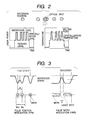
- a principle of the above-description is shown in FIG. 2 .
- the recording film is melt by use of a high laser power, the recording film is quenched after the irradiation, and thus a recording mark in an amorphous state is obtained even when a previous state of the recording film is crystalline or amorphous.
- the recording film is heated up to a temperature below a melting point, at which a crystallization rate is high, by use of an intermediate laser power, a part previously in the amorphous state turns into the crystalline state and a part originally in the crystalline state stays in the crystalline state as it is.
- a mark edge recording method is adopted, which can realize a high-density recording.
- positions of both edges of a recording mark formed on a recording film are made to correspond to digital data of 1. Accordingly, a length of a shortest recording mark is made to correspond not to one reference clock but to two to three reference clocks, thus enabling the high-density recording.
- an 8-16 modulation system is adopted, and the length of the recording mark is made to correspond to three reference clocks. As shown in a comparison of FIG.
- the mark edge recording method compared to a mark position recording in which a center position of a circle recording mark is made to correspond to the digital data of 1, the mark edge recording method has an advantage of capability of performing the high-density recording without reducing the recording mark to an extremely small size.
- Ws is a diameter of a beam spot
- Wm is a mark length
- d is a resolution.
- a DVD-RAM is a format in which 1 lap of track is divided into 24 sectors.
- the DVD-RAM can be used for various purposes from a storage device installed in a personal computer, a DVD video camera to a DVD video recorder.
- S is a number of sectors in a track.
- a track pitch can be made as narrow as 0.615 ⁇ m.
- phase difference between the recording mark and a portion other than the recording mark that is, a phase difference component of a reproduce signal acts in a direction where crosstalk is apt to occur, and thus it is required to design the phase difference component to be sufficiently small.
- the phase difference component of the reproduce signal is added to reflectivity-change reproduce signals of the land and the groove at the phase opposite to each other, resulting in unbalance of reproduce signal levels of the land and the groove.
- a phase-change recording medium when a recording waveform is not changed, it is desirable to record at an optimal linear velocity corresponding to a crystallization rate in order to obtain a satisfactory recording and reproducing characteristic.
- a ZCLV (zoned constant linear velocity) method is adopted, in which a radius direction of the disk is divided into 24 zones so as not to reduce an access speed, the revolution speed is kept constant in each zone, and the revolution speed is changed only when an access must be made to a different zone.
- linear velocities are slightly different between an innermost track in the zone and an outermost track therein, and thus recording densities thereof are slightly different from each other.
- recording is possible close to the maximum density all over the disk.
- a shortest mark length is 0.42 ⁇ m and a linear velocity is 8.2 m/s, and thus a recording pulse for forming one recording mark is divided into multiple parts.
- an emphasis is placed on precise heating rather than prevention of a buildup of heat, and as shown in FIG. 8 , a recording waveform is obtained, in which parts below a deleting power level are few or do not exist at all.
- an adaptive control of widths of the first pulse and the last pulse, which form the recording mark is also necessary.
- the adaptive control means that, in accordance with a length of a space, to which an attention is paid, and a length of a previous mark, adjustment is made for a position where a last pulse forming the previous mark ends and for a position where a first pulse forming a following mark starts.
- one layer has a plurality of roles, and functions of the respective layers are intricately intertwined with each other.
- the stress reduction by the thinning of the first protective layer prevents groove deformation, thus contributing to the making of the track pitch narrower. Therefore, the optimal selection of a combination of laminated films and the selection of film thickness are extremely important in offering the technical advantages.
- FIG. 1 is a section view schematically showing an example of an information recording medium according to the present invention.
- FIG. 2 is an explanatory view of a principle of overwriting.
- FIG. 3 is an explanatory view of mark position recording and mark edge recording.
- FIG. 4 is a schematic view showing header zones of a format of a substrate.
- FIG. 5 is a schematic view showing the format of the substrate.
- FIG. 6 is a schematic view showing zone disposition of the format of the substrate.
- FIG. 7 is a graph showing a relationship between the number of overwriting of the present invention and a jitter.
- FIG. 8 is a schematic view showing a relationship between adaptive control of a recording waveform and a mark length.
- FIG. 9 is a section view schematically showing an example of an information recording medium according to a comparative example.
- FIG. 10 is a graph showing a relationship among the number of overwriting of the present invention and the comparative example, a film thickness of a first protective layer and a ZnS additive amount.
- FIG. 11 is a graph showing a relationship among the number of the overwriting of the present invention, the film thickness of the first protective layer and the ZnS additive amount.
- FIG. 1 is a view showing a cross-section structure of a disk-shaped information recording medium according to a first embodiment of the present invention.
- the above medium is manufactured as described below.
- a first protective layer 2 made of (SiO 2 ) 60 ((In 2 O 3 ) 90 (SnO 2 ) 10 ) 25 (ZnS) 15 with a film thickness of 8 nm.
- a lower interface layer 3 made of a Cr 2 O 3 film is formed with a film thickness of 2 nm.
- a recording film 4 made of Ge 4 Sb 2 Te 7 with a film thickness of 8 nm
- a second protective layer 5 made of SnO 2 with a film thickness of 33 nm
- an absorption control layer 6 made of Cr 90 (Cr 2 O 3 ) 10 with a film thickness of 34 nm
- a reflective layer 7 made of Al with a film thickness of 60 nm.
- Cr 2 O 3 and SiO 2 one having a ratio of Cr and oxygen, which is slightly different from 2:3, and one having a ratio of Si and oxygen, which is slightly different from 1:2 are also called Cr 2 O 3 and SiO 2 .
- the slight difference refers to one within ⁇ 20%, and herein, the one having the ratio slightly different from 2:3 means one having a ratio in the range of 2:2.4 to 2:3.6.
- the information recording medium of the present invention is formed of laminated films of 6 layers or less, and the film formation thereof can be performed by use of a mass-production device having six chambers of a sputtering device.
- the all film thicknesses are 150 nm or less, and thus the present invention is extremely excellent in mass productivity compared to a conventional disk (comparative example 1) having a first protective layer with a thickness of 100 nm or more.
- Respective composition ratios are described in atomic % or mol %.
- the formation of the films is performed by use of a magnetron sputtering device using an Ar gas. Accordingly, a first disk member is obtained.
- a second disk member having the same constitution as the first disk member is obtained. Thereafter, protective coating by use of ultraviolet curing resin is performed on film surfaces of the first and second disk members, the respective ultraviolet curing resin layers thereof are attached to each other with an adhesive layer interposed therebetween, and the disk-shaped information recording medium shown in FIG. 1 is obtained.
- a protective substrate may be used instead of the second disk member.
- An initial crystallization is performed as below for the recording film of the disk manufactured as described above.
- the disk is rotated so as to have a linear velocity of a point on a recording track at 6 m/s, and by setting a laser beam power of an oblong semiconductor laser (a wavelength of about 810 nm), of which spot shape is long in a radius direction of the medium, to 600 mW, the recording film 4 is irradiated therewith through the substrate 1 . Movement of the spot is shifted by 1 ⁇ 4 of a spot length in the radius direction of the medium.
- the initial crystallization is thus performed. This initial crystallization may be performed once; however, by repeating the initial crystallization twice, a noise increase due to the initial crystallization can be reduced a little.
- an information recording and reproducing evaluation device By use of an information recording and reproducing evaluation device, recording and reproducing of information is performed for the foregoing recording medium.
- an operation of the information recording and reproducing evaluation device of the present invention will be described. Note that, for a motor control method in performing the recording and reproducing, the ZCLV (zoned constant linear velocity) method, in which the revolution speed of the disk is changed for each zone of performing the recording and reproducing, is adopted.
- a linear velocity of the disk is about 8.2 m/s.
- an 8-16 modulation method In recording information in a disk, a recording method for converting information of 8 bits to that of 16 bits, so-called an 8-16 modulation method is used to perform the recording.
- Information from outside of a recording device is transmitted to an 8-16 modulator while taking 8 bits as one unit.
- the recording of information is performed on the medium by use of recording mark lengths of 3T to 14T corresponding to the 8-bit information.
- “T” herein represents a clock cycle in the information recording, and the clock cycle is set to 17.1 ns here.
- Digital signals of 3T to 14T, which are converted by the 8-16 modulator, are transferred to a recording waveform generation circuit.
- the signals of 3T to 14T are made to correspond to “0” and “1” alternately in chronological order, a laser power of an intermediate power level is irradiated in the case of “0”, a high power pulse or a pulse train is irradiated in the case of “1”.
- a pulse train composed of a plurality of pulses with a high power level is used. Between the pulses of the pulse train, a laser of a low power level with a width of about T/2 is irradiated.
- the laser irradiation of the intermediate power level is performed, thus generating a multipulse recording waveform.
- the high power level for forming the recording mark is set to 11 mW
- the intermediate power level capable of deleting the recording mark is set to 5 mW
- the low power level lower than the intermediate power level is set to 5 mW.
- the low power level may be set to be the same as the intermediate power level or to be a different level.
- an area on the optical disk where the laser beam of the intermediate power level is irradiated is turned into a crystal (a space portion), and an area thereof where the pulse train of the high power level is irradiated is turned into an amorphous recording mark.
- a multipulse waveform table corresponding to a method for changing widths of first and last pulses in a multipulse waveform in accordance with lengths of the space portions before and after the mark portion (adaptive recording waveform control).
- the reflectivity of the recording medium a reflectivity thereof is higher in its crystalline state, and a reflectivity is low in the area recorded and turned into the amorphous state.
- the recording waveform generated in the recording waveform generation circuit is transferred to a laser drive circuit.
- the laser drive circuit changes an output power of the semiconductor laser in an optical head based on the transferred waveform.
- a laser beam with a wavelength of 660 nm is irradiated as an energy beam for information recording, thus performing the information recording.
- a mark length of the 3T mark, which is the shortest mark, is about 0.42 ⁇ m
- a mark length of the 14T mark, which is the longest mark is about 1.96 ⁇ m.
- dummy data composed of repetition of 4T marks and 4T spaces is included in a leader and a trailer of an information signal. In the leader thereof, VFO is also included.
- the recording device of the present invention corresponds to a method for recording information in both grooves and lands (areas between the grooves), so-called a land/groove (L/G) recording method.
- L/G land/groove
- tracking relative to the land and the groove can be arbitrarily selected.
- the recorded information is reproduced also by use of the foregoing optical head.
- a laser beam of 1 mW is irradiated on the recording track, and by detecting a light reflected from the mark and the portion other than the mark, a reproduce signal is obtained.
- the amplitude of the reproduce signal is increased by a preamplifier circuit, then converting into the 8-bit information for every 16 bits by an 8-16 demodulator.
- a recording pattern (random pattern) including 3T to 11T randomly is recorded, and a relationship between the number of overwriting and a jitter is investigated.
- a result shown in FIG. 7 is obtained.
- the jitter a value obtained by dividing an average value of the land and the groove by the clock cycle T is used.
- the jitter increases up to 13% or more.
- the jitter is 13% or less. Therefore, it is found out that the first protective layer described in the embodiment 1 prevents the substrate from being deteriorated and has a significant effect in increasing the number of possible rewrites.
- the first protective layer As a material of the first protective layer, SiO 2 is fixed to 60 mol % and a mol ratio of ITO((In 2 O 3 ) 90 (SnO 2 ) 10 ) and ZnS is changed. Meanwhile, a composition dependency of the number of possible rewrites is investigated. Moreover, the film thickness of the first protective layer is changed in respective compositions, and a film thickness dependency is investigated.
- Results thus obtained are shown in table 1 and FIG. 11 .
- a horizontal axis of table 1 indicates a ZnS amount (mol %), and a vertical axis thereof indicates the film thickness of the first protective layer (nm). In the table, the numbers of possible rewrites are shown.
- the film thickness of the first protective layer is in the range of 2 nm to 25 nm and the ZnS amount in the first protective layer is in the range of 4 mol % to 33 mol %, the number of possible rewrites can be increased as much as 300 times or more.
- the reason of the above finding will be described below. Specifically, by using a material of SiO 2 —In 2 O 3 —SnO 2 —ZnS series in the foregoing composition, optical characteristics are satisfied in the range where the film thickness is thin, including a reflectivity of 15% or more, a large contrast and the like.
- a thermal conductivity of the first protective layer is lowered by addition of ZnS, thus suppressing thermal conduction between the recording film and the substrate.
- a thermal characteristic for suppressing the substrate deterioration in the numerous rewritings is satisfied.
- the number of possible rewrites is 1000 times or more, which is equivalent to the number of possible rewrites of a DVD-RW and the like (about 1000 times) or more.
- the foregoing composition is preferable since both of the mass productivity and the rewriting property are included.
- the composition thus obtained is usable.
- the use of the material containing In 2 O 3 or SnO 2 enables DC sputtering because of a low electrical resistance of a target and realizes a shorter tact time, and thus the foregoing material is preferable.
- the DC sputtering is possible.
- the tact time is shorter than the conventional case of using (ZnS) 80 (SiO 2 ) 20 .
- the above-described materials are preferable. Even when the foregoing SnO 2 is entirely replaced by In 2 O 3 , a similar rewriting property is obtained. However, the DC sputtering is hard to perform in that case.
- the first protective layer is made of SiO 2 —In 2 O 3 —SnO 2 —ZnS, and a part of In 2 O 3 and/or SnO 2 and/or SiO 2 is replaced by any one of In—N, Sn—N, Al—N, Ta—N, Ti—N, Cr—N, Si—N and a nitride such as a mixture of the foregoing materials, the composition thus obtained is usable. As the amount of the nitride is increased, the film is likely to come off. Therefore, it is preferable that the replaced amounts of SiO 2 , In 2 O 3 and SnO 2 are less than 20 mol %, respectively.
- the impurity elements are preferably less than 5 atomic %, more preferably less than 3 atomic %.
- a recording film having any one of the following compositions including: a mixed composition of GeTe and Sb 2 Te 3 , such as Ge 2 Sb 2 Te 5 , Ge 7 Sb 4 Te 13 , Ge 4 Sb 2 Te 7 , Ge 5 Sb 2 Te 8 , Ge 6 Sb 2 Te 9 , Ge 8 Sb 2 Te 11 or the like; a composition close to the foregoing mixed composition, such as Ge 20 Sb 24 Te 56 or the like; a composition such as Ag 2 Ge 21 Sb 21 Te 56 , Sn 3 Ge 21 Sb 21 Te 55 , Sn 2 Ge 28 Sb 16 Te 54 , Sn 21 Ge 29 Sb 15 Te 54 Sn 3 Ge 33 Sb 11 Te 53 , Sn 3 Ge 36 Sb 9 Te 52 , Sn 7 Ge 19 Sb 19 Te 55 , Sn 8 Ge 25 Sb 14 Te 53 , Sn 8 Ge 26 Sb 13 Te 53 , Sn 7 Ge 30 Sb 10 Te 53 , Sn 8 Ge 32 S
- the impurity elements are preferably less than 5 atomic %, more preferably less than 2 atomic %.
- a recording film having a composition, of which main component is Ge—Sb—Te series can be also used, the composition including: Bi 3 Ge 21 Sb 21 Te 55 , Bi 2 Ge 28 , Sb 16 Te 54 , Bi 2 Ge 29 Sb 15 Te 54 , Bi 3 Ge 33 Sb 11 Te 53 , Bi 3 Ge 36 Sb 9 Te 52 , Bi 7 Ge 19 Sb 19 Te 55 , Bi 8 Ge 25 Sb 14 Te 53 , Bi 8 Ge 26 Sb 13 Te 53 , Bi 7 Ge 30 Sb 10 Te 53 , Bi 8 Ge 32 Sb 8 Te 52 and a composition close to the foregoing compositions.
- a recording film in which an additive element is added to the foregoing composition can be used. However, the number of possible rewrites is lowered by 10%.
- the thickness of the recording film is preferably 5 nm or more.
- the thickness of the recording film is 13 nm or more, which is too thick, a recrystallization area becomes too large. Accordingly, the jitter exceeds 13% after overwrites of 10 times.
- the thickness of the recording film is preferably less than 13 nm.
- the interface layer has a function of increasing the number of possible rewrites.
- the interface layer has an advantage as the following and the like.
- the interface layer can be formed by use of atmospheric gas including only Ar and is excellent in adhesiveness with other layers.
- a nitride such as a Ta—O series material, a Ge—Cr—N series material having a composition of Ge 50 Cr 10 N 40 and the like and including Ge or Si by 30 atomic % to 60 atomic % and Cr by 5 atomic % to 20 atomic %, a Si—Cr—N series material, a Ge—Si—Cr—N series material, a Ti—N series material such as Ti 60 N 40 and the like, a Ta—N series material such as Ta 55 N 45 and the like, a Sn—N series material such as Sn 70 N 30 and the like, the effect of improving the crystallization rate is large.
- the number of possible rewrites is reduced by 20% to 30%.
- the reduction in the number of possible rewrites is suppressed, compared to the case of replacing the same entirely.
- the effect of improving the crystallization rate is somewhat small.
- a Ge-containing composition such as GeN, GeO and the like is preferable because a sputtering rate thereof in film formation is faster than the others, thus enabling the tact time in manufacturing to be shortened. Note that the material cost thereof is relatively expensive.
- SiO 2 , Al 2 O 3 , Ta 2 O 5 and a mixture of Ta 2 O 5 and Cr 2 O 3 , Cr—N, Ge—N or Ge—O are preferable.
- ZnO, ZrO 2 , Y 2 O 3 , Cr 2 O 3 and a mixture of Cr—N, Ge—N and Ta 2 O 5 are preferable.
- CoO, Cr 2 O and NiO are more preferable because particle diameters in the initial crystallization become uniform and a jitter increase in the early stage of the rewriting is small.
- an AlN, BN, CrN, Cr 2 N, GeN, HfN, Si 3 N 4 or Al—Si—N series material for example, AlSiN 2
- an Si—N series material, Si—O—N series material and a nitride such as TaN, TiN, ZrN and the like are preferable because adhesivity is increased and deterioration of the information recording medium due to an external impact is reduced.
- a Cr 2 O 3 —ZnS interface layer obtained by adding ZnS to Cr 2 O 3 has an effect of improving a recording sensitivity.
- the addition of ZnS causes reduction in reflectivity in the numerous rewritings. When the ZnS amount is too much, the reflectivity is reduced by 5% or more in the numerous rewritings. Thus, the ZnS amount needs to be less than 15 mol %.
- the interface layer with the film thickness of 1 nm or more has an effect of avoiding appearance of an adverse influence in which the protective layer material such as ZnS diffuses into the recording film after many times of overwrites and has an effect of improving adhesiveness.
- the thickness of the interface layer is desirably 2 nm or more.
- the thickness of the interface layer made of Cr 2 O 3 exceeds 3 nm, light absorption of the layer causes a problem such as reduction in reflectivity.
- the thickness thereof is desirably 5 nm or less.
- the thickness thereof may be slightly thicker than the above, for example 7 nm.
- the film thickness of the interface layer on the side where light is made incident is preferably in the range of 1 nm to 8 nm.
- the protective layer, which is in contact with the interface layer is an oxide or a nitride
- the interface layer is used for the purpose of improving the adhesiveness because the protective layer has the effect of improving the crystallization rate. Therefore, when 40 mol % or more of the first protective layer is made of an oxide, an oxide-nitride or a nitride, the thickness of the interface layer on the side where light is made incident is preferably in the range of 1 nm to 3 nm.
- an interface layer of, for example, Ge—Cr—N which is lower in absorptivity than Cr 2 O 3 , there is no problem even when the interface layer has a much thicker film thickness.
- the material of the interface layer has a low sputtering rate, it is preferably to set the thickness thereof to 20 nm from the viewpoint of productivity.
- the impurity elements When impurity elements become 5 atomic % or more with respect to the constituent elements of the interface layer, the crystallization rate is lowered and a jitter increase in overwriting becomes 1% or more.
- the impurity elements are preferably less than 5 atomic %, more preferable less than 3 atomic %.
- the reflective layer in order to adjust an absorptivity ratio and maintain a high contrast, Cr, Al, In, Ni, Mo, Pt, Pd, Ti, W, Ge, Sb, Bi, and an alloy or a compound, which contain any of the above elements, are used. A content of these elements in the alloy or the compound is preferably 50 atomic % or more.
- the reflective layer moderately absorbs light and moderately filters out the light. Thus, light permeating through the recording film in the recording mark portion where the reflectivity is low is reflected on the reflective layer and absorbed again by the recording film, thereby preventing a temperature from being excessively increased and enabling Ac/Aa to be 1 or more.
- Ac and Aa indicate absorption coefficients of crystalline state and of amorphous state, respectively.
- Ac/Aa is an absorption rate of a recording film.
- Forming the reflective layer of an alloy containing at least one element among Au, Ag, Cu and Al in order to adjust the thermal diffusion has an effect in quality improvement of the reproduce signal.
- a cross erase in which a part of recording marks already written in adjacent tracks is deleted.
- a thermal diffusion in a longitudinal direction is important.
- the diffusion in the longitudinal direction hinders heat from going to the direction of the adjacent track. If Ac/Aa is larger than 1, a temperature increase in a recording mark portion of the adjacent track is reduced, thus leading to a good solution from the view point of the cross erase prevention.
- the material of the reflective layer preferable are: one having Cr or Cr alloy as a main component, including Cr, Cr—Al, Cr—Ag, Cr—Au, Cr—Ge and Cr—Ti; one having a Al alloy as a main component, such as Al—Ti, Al—Cr, Al—In and the like; Ge—Cr; Ge—Si; and Ge—N.
- one having Co, Ni, Mo, Pt, W, Ge, Sb, Bi, Ag, Au or Cu as a main component is also usable.
- One having an Ag alloy as a main component such as Ag—Pd, Ag—Cr, Ag—Ti, Ag—Pt, Ag—Cu, Ag—Pd—Cu and the like, one having an Au alloy as a main component such as Au—Cr, Au—Ti, Au—Ag, Au—Cu, Au—Nd and the like, and one having a Cu alloy as a main component are also high in reflectivity and satisfactory in a reproducing property.
- Pt and Au are noble metals and are thus expensive. In some cases, the two elements increase the cost compared to Cr, Al, Co, Ni, Mo, Ag, W, Ge, Sb and Bi.
- the impurity elements are 5 atomic % or more with respect to the constituent elements of the reflective layer, the thermal conductivity is lowered and a jitter increase in the numerous rewritings becomes large.
- the impurity elements are preferably less than 5 atomic %, more preferably less than 3 atomic %.
- the film thickness of the reflective layer is preferably in the range of 10 nm to 70 nm.
- the thickness thereof is too thin, a degree of modulation is reduced, and a jitter increase occurs in the numerous rewritings due to insufficient cooling of the heat.
- the absorptivity ratio is small, a jitter increase occurs in the overwriting, and groove deformation occurs due to stress of the substrate.
- a Sn—O or Sn—O—N material such as SnO 2 and the like
- a Sn—Si—O, Sn—Si—N or Sn—Si—O—N material such as SnO 2 —SiO 2 , SnO 2 —Si 3 N 4 , SnO 2 —SiO 2 —Si 3 N 4 and the like
- a Sn—Al—O, Sn—Al—N or Sn—Al—O—N material such as SnO 2 —Al 2 O 3 , SnO 2 —AlN, SnO 2 —Al 2 O 3 —AlN and the like
- a Sn—Cr—O, Sn—Cr—N or Sn—Cr—O—N material such as SnO 2 —Cr 2 O 3 , SnO 2 —CrN, SnO 2 —Cr 2 O 3 —CrN and the like
- the Sn—O or Sn—O—N material has extremely fast film formation rate, which is approximately twice as fast as (ZnS) 80 (SiO 2 ) 20 , which is the conventional material, and is preferable in terms of its suitability to mass production. Moreover, when the Sn—O or Sn—O—N material in the mixed material occupies 70 mol % or more of the total composition, the film formation rate is about 1.5 times as fast as that of (ZnS) 80 (SiO 2 ) 20 .
- the Sn—Gd—O, Sn—Gd—N or Sn—Gd—O—N material, the Sn—Bi—O, Sn—Bi—N or Sn—Bi—O—N material and the Sn—Zr—O, Sn—Zr—N or Sn—Zr—O—N material also have a high stability.
- the above materials are lower in the sputtering rate by about 10% than the Sn—Cr—O or Sn—Cr—O—N material and the Sn—Mo—O or Sn—Mn—O—N material.
- the adhesivity thereof with the recording film is increased, thus improving its storage life.
- the Sn—Mo—O or Sn—Mo—O—N material is used instead of the Sn—Ge—O, Sn—Ge—N or Sn—Ge—O—N material, a similar effect can be obtained.
- the Sn—In—O, Sn—In—N or Sn—In—O—N material has a low electrical resistance, thus having an advantage that the DC sputtering can be performed therefor.
- the sputtering rate can be increased twice as much.
- the DC sputtering can be performed.
- the Sn—O—Zn—S material obtained by adding ZnS to SnO 2 is also usable.
- thermal diffusivity can be lowered, thus lowering reduction in the recording sensitivity.
- a composition ratio of a mixed material of materials with a high thermal conductivity which are SiO 2 , Al 2 O 3 , Cr 2 O 3 and Ta 2 O 5 , is preferably 30 mol % or less.
- ZnS ZnS
- the sputtering rate is increased, and thus production tact can be shortened.
- the sputtering rate is increased by 10%.
- An amount of the mixed ZnS is preferably 30 mol % or less. If the amount of ZnS is out of the above range, the jitter increase in rewriting becomes 1% or more.
- mixing of a material including a nitrogen compound is also possible, the material including the Ge—Cr—N series material such as Ge 50 Cr 10 N 40 or the like, the Si—Cr—N series material such as Si 50 Cr 10 N 40 or the like.
- the sputtering rate is low, and thus the productivity is lowered to some extent.
- the impurity elements are 5 atomic % or more with respect to constituent elements of the second protective layer, a contrast is lowered and a jitter is increased.
- the impurity elements are preferably less than 5 atomic %, more preferably less than 3 atomic %.
- a preferable thickness of the second protective layer is in the range of 25 nm to 45 nm, more preferably in the range of 28 nm to 40 nm.
- the same condition as described above is established regarding the overwrite property even when the second protective layer is thicker at a 1 ⁇ 2 cycle of a value obtained by dividing a wavelength by a refraction index.
- deformation and a clack of the substrate occur due to the stress of the film, and time required for film formation gets long, which is unpractical.
- the reflectivity of the medium when the reflectivity of the medium is lower than 15%, there occur problems such as that a degree of modulation of a recording and reproducing signal is low, that recording and reproducing cannot be performed due to instability of AF and tracking, and the like.
- the reflectivity of the medium is preferably 15% or more. From the reasons described above and the like, also in the DVD-RAM standard, the reflectivity is decided to be 15% or more.
- the following materials may be used, including: an oxide such as SiO 2 , SiO, Al 2 O 3 , BeO, Bi 2 O 3 , CoO, CaO, CeO 2 , Cu 2 O, CuO, CdO, Dy 2 O 3 , FeO, Fe 2 O 3 , Fe 3 O 4 , GeO, GeO 2 , HfO 2 , In 2 O 3 , La 2 O 3 , MgO, MnO, MoO 2 , MoO 3 , NbO, NbO 2 , NiO, PbO, PdO, SnO, SnO 2 , Sc 2 O 3 , SrO, ThO 2 , TiO 2 , Ti 2 O 3 , TiO, Ta 2 O 5 , TeO 2 , VO, V 2 O 3 , VO 2 , WO 2 , WO 3 , Y 2 O 3 ,
- any of the above-described oxides enables use of a less expensive target than the others, thus enabling reduction in the total manufacturing cost.
- the oxides SiO 2 and Ta 2 O 5 are preferable because these two are low in reactivity, and thus the number of possible rewrites is further increased.
- Al 2 O 3 is high in thermal conductivity, when Al 2 O 3 is used in a disk having a structure with or without a reflective layer, deterioration of a rewriting property is smaller than the other cases.
- Cr 2 O 3 is preferable because both of a melting point thereof and a thermal conductivity thereof are high.
- any of the above-described sulfides enables the sputtering rate to be increased, thus enabling to shorten the film formation time.
- the use of any of the above-described carbides increases hardness of the absorption control layer and also brings about a function of suppressing flow of the recording film in the numerous rewritings.
- both of the metal element and/or a dielectric material have melting points higher than a melting point (about 600 degrees Celsius) of the recording film, a jitter increase after rewrites of 10000 times is reduced.
- the melting points of the both are 600 degrees Celsius or higher, the jitter increase can be suppressed to 3% or less, which is preferable.
- the polycarbonate substrate 1 is used, which has the tracking grooves directly on its surface.
- the substrate having the tracking grooves is a substrate having grooves of a depth of ⁇ /10n′ (n′ is a refraction index of a substrate material) or more in a part of or all over its surface when a recording and reproducing wavelength is set as ⁇ .
- the groove may be formed to be continuous in a lap or may be divided therein. It is found out that, when the groove depth is about ⁇ /6n′, a crosstalk is reduced, which is preferable.
- groove widths may be different from each other depending on positions thereof. If an inner groove has a narrower width, a problem is unlikely to occur in the numerous rewritings.
- the substrate of this embodiment may be a substrate having formats for recording and reproducing in both of the groove and the land or may be a substrate having the format for recording in either thereof.
- ultraviolet curing resin is applied onto the reflective layers of the first and second disk members in a thickness of about 10 ⁇ m before attachment of the members on each other and the attachment is performed after the resin is cured, the error rate can be lowered more.
- the two disk members are prepared, and the respective reflective layers 7 of the first and second disk members are attached to each other with the adhesive layer interposed therebetween.
- the substrate material is changed from polycarbonate to a material having polyolefin as a main component, it is preferable because rigidity of the substrate surface is increased and a deformation amount of the substrate due to heat is reduced by 10%. However, the material cost thereof increases twice or more.
- the tact of the lamination of the layers is decided depending on the sputtering rate of the respective films and the film thicknesses of the laminated layers.
- the tact to be rate controlling is 9 seconds.
- description for the additives of the first protective layer is omitted.
- the disk of the present invention is much superior to the conventional disk from the viewpoint of the mass production.
- a disk (comparative example 1) which is different from the disk of the embodiment 1 only in the first protective layer, is prepared, and the tact is compared therebetween by a similar method to the embodiment 1. Then, the following result is obtained.
- the lamination tact is 40 seconds, which is decided depending on a sputtering rate of a material constituting each of the layers and a film thickness of the laminated layer.
- the tact In a film formation device having seven chambers or more, the tact can be further shortened.
- the foregoing device is much more expensive than the one with six chambers, which is widespread in manufacturers, and thus a manufacturing cost thereof is high.
- a disk, in which the thickness of the first protective layer and the ZnS amount are changed, is prepared, and the number of possible rewrites is investigated. Then, the result of the embodiment 1 and a result in the vicinity of the comparative example 1 are shown in FIG. 10 .
- the number of possible rewrites is large.
- the formation of the first protective layer takes long.
- the first protective layer is as thick as 100 nm or more, deformations caused by the stress acting between the laminated films and the substrate are different between the pre-format portion and the user data portion, thus bringing about a state where the recording track bends toward the pre-format portion.
- the address data in the pre-format portion are unreadable.
- a disk (comparative example 2), which is different from the disk of the embodiment 1 only in the material of the first protective layer, is prepared, and a jitter in the numerous rewritings is measured by use of a similar method to the embodiment 1. Then, as shown in FIG. 7 , the jitter increases to 13% or more after overwrites of more than 100 times.
- a first protective layer 2 made of (SiO 2 ) 60 ((In 2 O 3 ) 90 (SnO 2 ) 10 ) 40 is formed with a film thickness of 8 nm.
- sputtering is performed in an Ar gas atmosphere.
- a disk which is different from the disk of the embodiment 1 only in the first protective layer, is prepared, and a jitter in the numerous rewritings is measured by use of a similar method to the embodiment 1. Then, similar to the embodiment 1, an effect that a jitter in random pattern recording after overwrites of 1000 times can be reduced to 13% or less is obtained.
- a first protective layer 2 made of (SiO 2 ) 60 ((In 2 O 3 ) 90 (SnO 2 ) 10 ) 25 (ZnS) 15 is formed with a film thickness of 8 nm.
- sputtering is performed by use of a mixed gas containing 10% (volume ratio) of CO 2 in an Ar gas.
- CO 2 or a chemical compound of C is added into the first protective layer, thus obtaining an effect of increasing the number of possible rewrites.
- CO 2 or the chemical compound of C is added to the first protective layer material by at least 0.1 atomic % or more, an effect of increasing the number of possible rewrites by 10% is obtained.
- the addition amount thereof is 2 atomic % or more, density of the first protective layer is lowered, thus lowering strength thereof. Therefore, the addition amount is preferably less than 2 atomic %.
- the gas for adding C in the film CH 4 , CS 2 and the like are also usable.
- the gas mixed with CO 2 is preferable, because the foregoing gas is inexpensive as the mixed gas used in the production, thus suppressing the increase in the total production cost.
- the reason why the number of possible rewrites is increased is because, when C or the chemical compound of C is added into the first protective layer, the thermal conductivity of the first protective layer is lowered, and thus heat is unlikely to be transmitted into the substrate, a temperature increase of the substrate in rewriting is prevented and deterioration of the substrate is prevented.
- a first protective layer according to the embodiment 5 is formed of (SiO 2 ) 60 ((In 2 O 3 ) 90 (SnO 2 ) 10 ) 25 (ZnS) 15 .
- sputtering is performed by setting a flow rate of the Ar gas used in the sputtering to twice as much as a normal rate or more, for example 400 sccm or more, thus forming the first protective layer.
- Ar is contained in the first protective layer, and thus the effect of increasing the number of possible rewrites is obtained.
- Ar is added to the first protective layer material by at least 0.1 atomic % or more, an effect of increasing the number of possible rewrites by 10% is obtained.
- the addition amount thereof is 2 atomic % or more, density of the first protective layer is lowered, thus lowering strength thereof. Therefore, the addition amount is preferably less than 2 atomic %.
- the Ar gas is preferable, because the Ar gas is less expensive than the mixed gas, He, Ne, Kr and Xe, thus suppressing the increase in the total production cost.
- the reason why the number of possible rewrites is increased is because, when Ar or He, Ne, Kr or Xe is added into the first protective layer, the thermal conductivity of the first protective layer is lowered, and thus heat is unlikely to be transmitted into the substrate, the temperature increase of the substrate in rewriting is prevented and the deterioration of the substrate is prevented.
- an information recording medium for performing high-density recording and reproducing a medium, which enables film formation by use of a film formation device with six chambers, is excellent in material costs and mass productivity and has satisfactory recording and reproducing characteristic and rewriting property, can be obtained.
Applications Claiming Priority (2)
| Application Number | Priority Date | Filing Date | Title |
|---|---|---|---|
| JP2002230756A JP2004071079A (ja) | 2002-08-08 | 2002-08-08 | 情報記録媒体 |
| JP2002-230756 | 2002-08-08 |
Publications (2)
| Publication Number | Publication Date |
|---|---|
| US20040027982A1 US20040027982A1 (en) | 2004-02-12 |
| US6854126B2 true US6854126B2 (en) | 2005-02-08 |
Family
ID=31492342
Family Applications (1)
| Application Number | Title | Priority Date | Filing Date |
|---|---|---|---|
| US10/345,231 Expired - Fee Related US6854126B2 (en) | 2002-08-08 | 2003-01-16 | Information recording medium with SiO2-In2O3-SnO2-ZnS protective layer |
Country Status (4)
| Country | Link |
|---|---|
| US (1) | US6854126B2 (zh) |
| JP (1) | JP2004071079A (zh) |
| CN (1) | CN1474390A (zh) |
| TW (1) | TW200402707A (zh) |
Cited By (6)
| Publication number | Priority date | Publication date | Assignee | Title |
|---|---|---|---|---|
| US20030174610A1 (en) * | 2002-03-13 | 2003-09-18 | Hitachi, Ltd. | Information recording media, manufacturing technique and information recording method |
| US20050018593A1 (en) * | 2003-07-25 | 2005-01-27 | Matsushita Electric Industrial Co., Ltd. | Information recording medium and method for producing the same |
| US20050084799A1 (en) * | 2002-02-14 | 2005-04-21 | Masataka Yahagi | Sputtering target containing zinc sulfide as major component, optical recording medium on which phase change optical disk protective film containing zinc sulfide as major component is formed by using the target, and method for manufacturing the sputtering target |
| US20090246558A1 (en) * | 2005-12-02 | 2009-10-01 | Takashi Nishihara | Information recording medium and method for manufacturing the same |
| US20100068444A1 (en) * | 2008-09-12 | 2010-03-18 | Asplund Matthew C | Data storage containing carbon and metal layers |
| US20100068529A1 (en) * | 2008-09-12 | 2010-03-18 | Asplund Matthew C | Films containing an infused oxygenated as and methods for their preparation |
Families Citing this family (8)
| Publication number | Priority date | Publication date | Assignee | Title |
|---|---|---|---|---|
| JP2004327007A (ja) * | 2003-04-08 | 2004-11-18 | Nec Corp | 光学的情報記録媒体および光学的情報記録再生装置 |
| EP2028287B1 (en) * | 2004-02-17 | 2012-08-22 | JX Nippon Mining & Metals Corporation | Sputtering target |
| JP2005251279A (ja) * | 2004-03-03 | 2005-09-15 | Nec Corp | 光学的情報記録媒体及びその製造方法 |
| JP2005302275A (ja) * | 2004-03-18 | 2005-10-27 | Sharp Corp | 光情報記録媒体、記録再生方法、ならびに記録再生装置 |
| JP4136980B2 (ja) * | 2004-03-19 | 2008-08-20 | 株式会社リコー | 多層相変化型情報記録媒体及びその記録再生方法 |
| DE602006019886D1 (de) * | 2005-09-05 | 2011-03-10 | Ricoh Co Ltd | Mehrschichtiges optisches aufzeichnungsmedium und optisches aufzeichnungsverfahren |
| JP5617403B2 (ja) * | 2010-07-15 | 2014-11-05 | ソニー株式会社 | 光記録媒体 |
| EP3360139A4 (en) | 2015-10-05 | 2019-10-23 | Shanghai Naguang Information Technology Corporation | MEDIA, SYSTEMS AND METHOD FOR OPTICAL DATA STORAGE |
Citations (5)
| Publication number | Priority date | Publication date | Assignee | Title |
|---|---|---|---|---|
| JPS62239443A (ja) * | 1986-04-10 | 1987-10-20 | Seiko Epson Corp | 光記録媒体 |
| JPH03240590A (ja) * | 1990-02-20 | 1991-10-25 | Ricoh Co Ltd | 情報記録媒体 |
| JPH05174435A (ja) * | 1991-12-25 | 1993-07-13 | Tonen Corp | 光磁気記録媒体 |
| JPH05234133A (ja) * | 1992-02-25 | 1993-09-10 | Ricoh Co Ltd | 光情報記録媒体 |
| JP2001266408A (ja) | 2000-03-16 | 2001-09-28 | Toray Ind Inc | 光記録媒体およびその製造方法 |
-
2002
- 2002-08-08 JP JP2002230756A patent/JP2004071079A/ja not_active Withdrawn
- 2002-11-29 TW TW091134775A patent/TW200402707A/zh unknown
-
2003
- 2003-01-16 US US10/345,231 patent/US6854126B2/en not_active Expired - Fee Related
- 2003-01-20 CN CNA031018661A patent/CN1474390A/zh active Pending
Patent Citations (5)
| Publication number | Priority date | Publication date | Assignee | Title |
|---|---|---|---|---|
| JPS62239443A (ja) * | 1986-04-10 | 1987-10-20 | Seiko Epson Corp | 光記録媒体 |
| JPH03240590A (ja) * | 1990-02-20 | 1991-10-25 | Ricoh Co Ltd | 情報記録媒体 |
| JPH05174435A (ja) * | 1991-12-25 | 1993-07-13 | Tonen Corp | 光磁気記録媒体 |
| JPH05234133A (ja) * | 1992-02-25 | 1993-09-10 | Ricoh Co Ltd | 光情報記録媒体 |
| JP2001266408A (ja) | 2000-03-16 | 2001-09-28 | Toray Ind Inc | 光記録媒体およびその製造方法 |
Cited By (11)
| Publication number | Priority date | Publication date | Assignee | Title |
|---|---|---|---|---|
| US20050084799A1 (en) * | 2002-02-14 | 2005-04-21 | Masataka Yahagi | Sputtering target containing zinc sulfide as major component, optical recording medium on which phase change optical disk protective film containing zinc sulfide as major component is formed by using the target, and method for manufacturing the sputtering target |
| US7279211B2 (en) * | 2002-02-14 | 2007-10-09 | Nippon Mining & Metals Co., Ltd. | Sputtering target containing zinc sulfide as major component, optical recording medium on which phase change optical disk protective film containing zinc sulfide as major component is formed by using the target, and method for manufacturing the sputtering target |
| US20030174610A1 (en) * | 2002-03-13 | 2003-09-18 | Hitachi, Ltd. | Information recording media, manufacturing technique and information recording method |
| US7041430B2 (en) * | 2002-03-13 | 2006-05-09 | Hitachi, Ltd. | Information recording media, manufacturing technique and information recording method |
| US20050018593A1 (en) * | 2003-07-25 | 2005-01-27 | Matsushita Electric Industrial Co., Ltd. | Information recording medium and method for producing the same |
| US7255906B2 (en) * | 2003-07-25 | 2007-08-14 | Matsushita Electric Industrial Co., Ltd. | Information recording medium and method for producing the same |
| US20090246558A1 (en) * | 2005-12-02 | 2009-10-01 | Takashi Nishihara | Information recording medium and method for manufacturing the same |
| US8075973B2 (en) | 2005-12-02 | 2011-12-13 | Panasonic Corporation | Information recording medium and method for manufacturing the same |
| US20100068444A1 (en) * | 2008-09-12 | 2010-03-18 | Asplund Matthew C | Data storage containing carbon and metal layers |
| US20100068529A1 (en) * | 2008-09-12 | 2010-03-18 | Asplund Matthew C | Films containing an infused oxygenated as and methods for their preparation |
| US8192820B2 (en) | 2008-09-12 | 2012-06-05 | Brigham Young University | Data storage media containing carbon and metal layers |
Also Published As
| Publication number | Publication date |
|---|---|
| CN1474390A (zh) | 2004-02-11 |
| US20040027982A1 (en) | 2004-02-12 |
| TW200402707A (en) | 2004-02-16 |
| JP2004071079A (ja) | 2004-03-04 |
Similar Documents
| Publication | Publication Date | Title |
|---|---|---|
| US6854126B2 (en) | Information recording medium with SiO2-In2O3-SnO2-ZnS protective layer | |
| JP4030205B2 (ja) | 情報記録媒体及び情報記録装置 | |
| US20050064334A1 (en) | Information recording medium | |
| US6723411B2 (en) | Information recording medium and method for manufacturing an information recording medium | |
| US6703098B2 (en) | Information recording medium and method for manufacturing information recording medium | |
| US6806030B2 (en) | Information recording medium and method for manufacturing information recording medium | |
| TWI246078B (en) | Information recording medium | |
| JP4124535B2 (ja) | 光学情報記録媒体およびその記録再生方法 | |
| JP2003228881A (ja) | 情報記録媒体 | |
| JP2005302263A (ja) | 光ディスク及びその記録再生装置並びにアドレス情報管理方法 | |
| JP3653390B2 (ja) | 情報記録媒体 | |
| JP3786665B2 (ja) | 情報記録媒体 | |
| JP3654897B2 (ja) | 情報記録媒体 | |
| JP3655298B2 (ja) | 情報記録媒体 | |
| JP2006286043A (ja) | 情報記録媒体 | |
| JP2007157202A (ja) | 光記録媒体、及びその初期化方法 | |
| JP4214155B2 (ja) | 光学情報記録媒体及びその記録再生方法 | |
| JP2001344807A (ja) | 情報記録媒体 | |
| JP4282706B2 (ja) | 情報記録媒体 | |
| JP3877756B2 (ja) | 情報記録媒体 | |
| JP2005193663A (ja) | 光記録媒体 | |
| JP2001101712A (ja) | 情報記録媒体及び情報記録装置 | |
| JP4156811B2 (ja) | 情報記録媒体 | |
| JPH11288526A (ja) | 情報記録媒体 | |
| JP2005246625A (ja) | 光情報記録媒体 |
Legal Events
| Date | Code | Title | Description |
|---|---|---|---|
| AS | Assignment |
Owner name: HITACHI, LTD., JAPAN Free format text: ASSIGNMENT OF ASSIGNORS INTEREST;ASSIGNORS:HIROTSUNE, AKEMI;TERAO, MOTOYASU;ANZAI, YUMIKO;REEL/FRAME:015238/0236;SIGNING DATES FROM 20031128 TO 20031205 |
|
| REMI | Maintenance fee reminder mailed | ||
| LAPS | Lapse for failure to pay maintenance fees | ||
| STCH | Information on status: patent discontinuation |
Free format text: PATENT EXPIRED DUE TO NONPAYMENT OF MAINTENANCE FEES UNDER 37 CFR 1.362 |
|
| FP | Lapsed due to failure to pay maintenance fee |
Effective date: 20090208 |