US6850232B2 - Semiconductor device capable of internally generating bias changing signal - Google Patents
Semiconductor device capable of internally generating bias changing signal Download PDFInfo
- Publication number
- US6850232B2 US6850232B2 US10/225,865 US22586502A US6850232B2 US 6850232 B2 US6850232 B2 US 6850232B2 US 22586502 A US22586502 A US 22586502A US 6850232 B2 US6850232 B2 US 6850232B2
- Authority
- US
- United States
- Prior art keywords
- signal
- circuit
- counter
- bias
- bit counter
- Prior art date
- Legal status (The legal status is an assumption and is not a legal conclusion. Google has not performed a legal analysis and makes no representation as to the accuracy of the status listed.)
- Expired - Fee Related, expires
Links
Images


Classifications
-
- G—PHYSICS
- G09—EDUCATION; CRYPTOGRAPHY; DISPLAY; ADVERTISING; SEALS
- G09G—ARRANGEMENTS OR CIRCUITS FOR CONTROL OF INDICATING DEVICES USING STATIC MEANS TO PRESENT VARIABLE INFORMATION
- G09G3/00—Control arrangements or circuits, of interest only in connection with visual indicators other than cathode-ray tubes
- G09G3/20—Control arrangements or circuits, of interest only in connection with visual indicators other than cathode-ray tubes for presentation of an assembly of a number of characters, e.g. a page, by composing the assembly by combination of individual elements arranged in a matrix no fixed position being assigned to or needed to be assigned to the individual characters or partial characters
- G09G3/34—Control arrangements or circuits, of interest only in connection with visual indicators other than cathode-ray tubes for presentation of an assembly of a number of characters, e.g. a page, by composing the assembly by combination of individual elements arranged in a matrix no fixed position being assigned to or needed to be assigned to the individual characters or partial characters by control of light from an independent source
- G09G3/36—Control arrangements or circuits, of interest only in connection with visual indicators other than cathode-ray tubes for presentation of an assembly of a number of characters, e.g. a page, by composing the assembly by combination of individual elements arranged in a matrix no fixed position being assigned to or needed to be assigned to the individual characters or partial characters by control of light from an independent source using liquid crystals
- G09G3/3611—Control of matrices with row and column drivers
- G09G3/3685—Details of drivers for data electrodes
- G09G3/3688—Details of drivers for data electrodes suitable for active matrices only
-
- G—PHYSICS
- G11—INFORMATION STORAGE
- G11C—STATIC STORES
- G11C5/00—Details of stores covered by group G11C11/00
- G11C5/14—Power supply arrangements, e.g. power down, chip selection or deselection, layout of wirings or power grids, or multiple supply levels
-
- H—ELECTRICITY
- H03—ELECTRONIC CIRCUITRY
- H03F—AMPLIFIERS
- H03F1/00—Details of amplifiers with only discharge tubes, only semiconductor devices or only unspecified devices as amplifying elements
- H03F1/02—Modifications of amplifiers to raise the efficiency, e.g. gliding Class A stages, use of an auxiliary oscillation
- H03F1/0205—Modifications of amplifiers to raise the efficiency, e.g. gliding Class A stages, use of an auxiliary oscillation in transistor amplifiers
- H03F1/0261—Modifications of amplifiers to raise the efficiency, e.g. gliding Class A stages, use of an auxiliary oscillation in transistor amplifiers with control of the polarisation voltage or current, e.g. gliding Class A
-
- H—ELECTRICITY
- H03—ELECTRONIC CIRCUITRY
- H03K—PULSE TECHNIQUE
- H03K5/00—Manipulating of pulses not covered by one of the other main groups of this subclass
- H03K5/003—Changing the DC level
-
- H—ELECTRICITY
- H03—ELECTRONIC CIRCUITRY
- H03K—PULSE TECHNIQUE
- H03K5/00—Manipulating of pulses not covered by one of the other main groups of this subclass
- H03K5/22—Circuits having more than one input and one output for comparing pulses or pulse trains with each other according to input signal characteristics, e.g. slope, integral
- H03K5/24—Circuits having more than one input and one output for comparing pulses or pulse trains with each other according to input signal characteristics, e.g. slope, integral the characteristic being amplitude
- H03K5/2472—Circuits having more than one input and one output for comparing pulses or pulse trains with each other according to input signal characteristics, e.g. slope, integral the characteristic being amplitude using field effect transistors
- H03K5/2481—Circuits having more than one input and one output for comparing pulses or pulse trains with each other according to input signal characteristics, e.g. slope, integral the characteristic being amplitude using field effect transistors with at least one differential stage
-
- G—PHYSICS
- G09—EDUCATION; CRYPTOGRAPHY; DISPLAY; ADVERTISING; SEALS
- G09G—ARRANGEMENTS OR CIRCUITS FOR CONTROL OF INDICATING DEVICES USING STATIC MEANS TO PRESENT VARIABLE INFORMATION
- G09G2310/00—Command of the display device
- G09G2310/02—Addressing, scanning or driving the display screen or processing steps related thereto
- G09G2310/0264—Details of driving circuits
- G09G2310/027—Details of drivers for data electrodes, the drivers handling digital grey scale data, e.g. use of D/A converters
Definitions
- the present invention relates to a semiconductor device such as a data line driver of a liquid crystal display (LCD) apparatus, and more particularly, to the improvement of generation of a bias changing signal for changing a bias current flowing through an operational amplifier (voltage follower) for driving a capacitive load.
- a semiconductor device such as a data line driver of a liquid crystal display (LCD) apparatus
- an operational amplifier voltage follower
- a plurality of voltage followers are provided to drive a plurality of capacitive loads such data lines in accordance with a control signal such as a strobe signal.
- a bias circuit controls bias currents flowing through the voltage followers in accordance with an externally-generated bias changing signal. That is, in a high access mode state, the bias currents are increased to increase the operation speed while the power consumption is increased. On the other hand, in a low access mode, the bias currents are decreased to decrease the operation speed while the power consumption is decreased. This will be explained later in detail.
- the bias changing signal in synchronization with the control signal has to be input as an external signal to the bias circuit, which is a burden on the user. Additionally, when the number of capacitive loads is increased, or when the resistance and capacity of the LCD panel fluctuates due to the manufacturing process thereof, the bias changing signal has to be adjusted by the user, which is another burden on the user.
- At least one operational amplifier drives a capacitive load in accordance with a control signal.
- a bias changing circuit receives the control signal to generate a bias changing signal in synchronization with the control signal dependent upon a width of the control signal.
- a bias circuit controls a bias current flowing through the operational amplifier in accordance with the bias changing signal.
- FIG. 1 is a circuit diagram illustrating a first prior art data line driver of an LCD apparatus
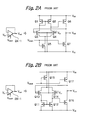
- FIG. 2A is a detailed circuit diagram of the voltage follower for a positive polarity driving operation of FIG. 1 ;
- FIG. 2B is a detailed circuit diagram of the voltage follower for a negative polarity driving operation of FIG. 1 ;
- FIG. 3 is a detailed circuit diagram of the bias circuit of FIG. 1 ;
- FIG. 4 is a circuit diagram illustrating a second prior art data line driver of an LCD apparatus
- FIG. 5 is a detailed circuit diagram of the voltage follower of FIG. 4 ;
- FIG. 6 is a circuit diagram illustrating a first embodiment of the data line driver of an LCD apparatus according to the present invention.
- FIG. 7 is a block circuit diagram of the bias changing circuit of FIG. 6 ;
- FIG. 8A is a timing diagram for explaining a first operation of the bias changing circuit of FIG. 7 ;
- FIG. 8B is a table showing the first operation of FIG. 8A ;
- FIG. 9A is a timing diagram for explaining a second operation of the bias changing circuit of FIG. 7 ;
- FIG. 9B is a table showing the second operation of FIG. 9A ;
- FIG. 10 is a circuit diagram illustrating a modification of the bias changing circuit of FIG. 7 ;
- FIG. 11 is a circuit diagram illustrating a second embodiment of the data line driver of an LCD apparatus according to the present invention.
- FIGS. 12 and 13 are block circuit diagrams illustrating modifications of the bias changing circuits of FIGS. 7 and 10 , respectively;
- FIGS. 14A and 14B are block circuit diagrams illustrating further modifications of the bias changing circuits of FIGS. 12 and 13 ;
- FIG. 15 is a block circuit diagram illustrating a modification of the bias changing circuit of FIG. 10 .
- reference numeral 1 designates a data line control circuit for receiving a digital video data signal DA, a clock signal CLK and a strobe signal STB, to generate multi-gradation analog data voltages V 1 , V 2 , . . . , V 383 and V 384 (or V 2 , V 1 , . . . , V 384 and V 383 ).
- the data line control circuit 1 is constructed by shift registers, data registers, latch circuits, level shifters, a multi-gradation voltage generating ladder circuit and a digital/analog (D/A) converter (not shown). Note that the strobe signal STB is also used for carrying out a dot inversion driving operation.
- the digital video data signal DA is input in series in synchronization with the clock signal CLK. Then, a serial-to-parallel conversion is performed upon the input digital video signal. Then, each parallel video digital signal is converted into a multi-gradation analog data voltage in synchronization with the strobe signal STB.
- the multi-gradation data voltages V 1 , V 2 , . . . , V 383 , V 384 (or V 2 , V 1 , . . . , V 384 , V 383 ) are supplied to voltage followers (operational amplifiers) 2 A- 1 , 2 A- 2 , . . . , 2 A- 192 and 2 B- 192 , respectively, for driving data lines D 1 , D 2 , . . . , D 383 and D 384 via switches 4 - 1 , . . . , 4 - 192 .
- the voltage followers 2 A- 1 , . . . , 2 A- 192 are used for carrying out a positive polarity driving operation, while the voltage followers 2 B- 1 , . . . , 2 B- 192 are used for carrying out a negative polarity driving operation.
- the voltage followers 2 A- 1 , . . . , 2 A- 192 alternate with the voltage followers 2 B- 1 , . . . , 2 B- 192 .
- the switches 4 - 1 , . . . , 4 - 192 are controlled by the data line control circuit 1 . That is, when the data line control circuit 1 generates multi-gradation data voltages V 1 , V 2 , . . . , V 383 , V 384 , the voltage followers 2 A- 1 and 2 B- 1 are connected to the data lines D 1 and D 2 , respectively; . . . ; the voltage followers 2 A- 192 and 2 B- 192 are connected to the data lines D 383 and D 384 , respectively. On the other hand, when the data line control circuit 1 generates multi-gradation data voltages V 2 , V 1 , . . .
- a bias circuit 5 receives a bias changing signal BIC to control bias voltages V biasA and V biasB of the voltage followers 2 A- 1 , . . . , 2 A- 192 and 2 B- 1 , . . . , 2 B- 192 . That is, the bias changing signal BIC is externally generated.
- FIG. 2A which is a detailed circuit diagram of the voltage follower 2 A- 1 ( 2 A- 192 ) of FIG. 1
- a differential amplifier powered by a high power line V DD and a low power line V SS is formed by load P-channel MOS transistors Q 1 and Q 2 , N-channel MOS transistors Q 3 and Q 4 , and an N-channel MOS transistor Q 5
- an output circuit powered by the high power line V DD and the low power line V SS is formed by a P-channel MOS transistor Q 6 and an N-channel MOS transistor Q 7 .
- the load P-channel MOS transistors Q 1 and Q 2 form a current mirror circuit.
- each of the N-channel MOS transistors Q 5 and Q 7 serves as a constant current source. Therefore, in a high bias mode, i.e., a high speed mode, when the bias voltage V biasA is high, the output voltage V out rises rapidly while the power consumption is increased. On the other hand, in a low bias mode, i.e., a low speed mode, when the bias voltage V biasA is low, the output voltage V out rises slowly while the power consumption is decreased.
- FIG. 2B which is a detailed circuit diagram of the voltage follower 2 B- 1 ( 2 B- 192 ) of FIG. 1
- a differential amplifier powered by the high power line V DD and the low power line V SS is formed by load N-channel MOS transistors Q 11 and Q 12 , P-channel MOS transistors Q 13 and Q 14 , and a P-channel MOS transistor Q 15
- an output circuit powered by the high power line V DD and the low power line V SS is formed by an N-channel MOS transistor Q 16 and a P-channel MOS transistor Q 17 .
- the load N-channel MOS transistors Q 11 and Q 12 form a current mirror circuit.
- each of the P-channel MOS transistors Q 15 and Q 17 serves as a constant current source. Therefore, in a high bias mode, i.e., a high speed mode, when the bias voltage V biasB is low, the output voltage V out falls rapidly while the power consumption is increased. On the other hand, in a low bias mode, i.e., a low speed mode, when the bias voltage V biasB is high, the output voltage V out falls slowly while the power consumption is decreased.
- FIG. 3 which is a detailed circuit diagram of the bias circuit 5 of FIG. 1 , the bias circuit 5 is constructed by a bias current circuit 51 for generating a bias current I B and a bias voltage generating circuit 52 for generating the bias voltages V biasA and V biasB in accordance with the bias current I B .
- the bias current circuit 51 is formed by P-channel MOS transistors Q 21 and Q 22 having ON resistances R 1 and R 2 (R 1 ⁇ R 2 ) connected in parallel to the high power line V DD and an inverter INV for selecting one of the P-channel MOS transistors Q 21 and Q 22 in accordance with the bias control signal BIC.
- the drains of the P-channel MOS transistors Q 21 and Q 22 are connected to the bias voltage generating circuit 52 .
- the bias voltage generating circuit 52 is formed by a current mirror circuit of N-channel MOS transistors Q 23 and Q 24 connected between the bias current circuit 51 and the low power line V SS , a current mirror circuit of P-channel MOS transistors Q 25 and Q 26 connected between the high power line V DD , and an N-channel MOS transistor Q 27 .
- a current flowing through the N-channel MOS transistor Q 23 i.e., a current flowing through the N-channel MOS transistor Q 24 is determined by a bias current I B of the bias current circuit 51 .
- a current flowing through the P-channel MOS transistor Q 25 i.e., a current flowing through the P-channel MOS transistor Q 26 is determined by the current flowing through the N-channel MOS transistor Q 24 .
- a current flowing through the N-channel MOS transistor Q 27 is determined by the current flowing the P-channel MOS transistor Q 26 .
- the bias voltage V biasA depends on the bias current I B .
- the bias voltage V biasB depends on the bias current I B .
- the bias current control signal BIC when the bias current control signal BIC is high, the P-channel MOS transistors Q 21 and Q 22 are turned ON and OFF, respectively, so as to increase the bias current I B . As a result, the currents flowing through the transistors Q 27 and Q 25 are increased, and therefore,
- the bias current control signal BIC when the bias current control signal BIC is low, the P-channel MOS transistors Q 21 and Q 22 are turned OFF and ON, respectively, so as to decrease the bias current I B . As a result, the currents flowing through the transistors Q 27 and Q 25 are decreased, and therefore,
- the bias changing signal BIC in synchronization with the strobe signal STB has to be input as an external signal to the bias circuit 5 , which is a burden on the user.
- the above-mentioned predetermined time period has to be adjusted by the user, which is another burden on the user.
- FIG. 4 which illustrates a second prior art data line driver of an LCD apparatus
- a data line control circuit 1 ′ is provided instead of the data line control circuit 1 of FIG. 1
- voltage followers 2 - 1 , 2 - 2 , . . . , 2 - 383 and 2 - 384 are provided instead of the voltage followers 2 A- 1 , 2 B- 1 , . . . , 2 A- 192 and 2 B- 192 and the switches 4 - 1 , 4 - 2 , . . . , 4 - 383 and 4 - 384 of FIG. 1 .
- V 383 and V 384 are supplied to the voltage followers 2 - 1 , 2 - 2 , . . . , 2 - 383 and 2 - 384 , respectively.
- the strobe signal STB is also used for carrying out a line inversion driving operation.
- each of the voltage followers 2 - 1 , 2 - 2 , 2 - 383 and 2 - 384 is constructed by a combination of the voltage follower 2 A- 1 ( 2 A- 192 ) of FIG. 2 A and the voltage follower 2 B- 1 ( 2 B- 192 ) of FIG. 2 B.
- a P-channel MOS transistor Q 51 forms a current mirror circuit with the P-channel MOS transistor Q 1 and is connected to the load N-channel MOS transistor Q 12 .
- a P-channel MOS transistor Q 52 forms a current mirror circuit with the P-channel MOS transistor Q 2 and is connected to the load N-channel MOS transistor Q 11 .
- the differential amplifier (Q 1 , Q 2 , . . . , Q 5 ) is combined with the differential amplifier (Q 11 , Q 12 , . . . , Q 15 ) by the P-channel MOS transistors Q 51 and Q 52 .
- the output voltage V d of the combined differential amplifiers is supplied via a level conversion circuit LC to the output P-channel MOS transistor Q 6 .
- the output voltage of the combined differential amplifiers is supplied directly to the output N-channel MOS transistor Q 16 .
- the level conversion circuit LC is constructed by load P-channel MOS transistors Q 53 and Q 54 , N-channel MOS transistors Q 55 , Q 56 and Q 57 .
- the N-channel MOS transistor Q 56 serves as a load.
- the bias changing signal BIC in synchronization with the strobe signal STB has to be input as an external signal to the bias circuit 5 , which is a burden on the user.
- the above-mentioned predetermined time period has to be adjusted by the user, which is another burden on the user.
- FIG. 6 which illustrates a first embodiment of the data line driver of an LCD apparatus according to the present invention
- a bias changing circuit 6 is added to the elements of FIG. 1 .
- the bias changing circuit 6 receives the strobe signal STB and the clock signal CLK to generate the bias changing signal BIC. That is, the bias changing signal BIC is internally generated.
- the bias changing circuit 6 receives a selection signal SEL to change the predetermined time period of a high access mode (high power consumption mode) in accordance with the number of data lines and/or the fluctuation of the resistance and capacitance of an LCD panel. Note that since the selection signal SEL is set to be low or high, the selection signal SEL can be easily set by the user.
- the bias changing circuit 6 is constructed by an 8-bit counter 61 for counting the pulses of the clock signal CLK, a 9-bit counter 62 for counting the pulses of the clock signal CLK, a comparator 63 for comparing the three most significant bits (2 5 , 2 6 , 2 7 ) of the output signal of the counter 62 except for the most significant bit (2 8 ) thereof with the three most significant bits (2 5 , 2 6 , 2 7 ) of the output signal of the counter 61 , a comparator 64 for comparing the three most significant bits (2 6 , 2 7 , 2 8 ) of the output signal of the counter 62 with the three most significant bits (2 5 , 2 6 , 2 7 ) of the output signal of the counter 61 , a selector 65 for selecting one of the comparators 63 and 64 in accordance with the selection signal SEL, and a flip-flop 66 which is set by a rising edge of the
- the 8-bit counter 61 is reset and enabled by a rising edge of the strobe signal STB, and the operation of the 8-bit counter 61 is stopped by a falling edge of the strobe signal STB. Also, the 9-bit counter 62 is reset and enabled by a falling edge of the strobe signal STB.
- the selector 65 selects the comparator 63 .
- the selector 65 selects the comparator 64 . In both of the comparators 63 and 64 , when the value of the predetermined three bits of the counter 62 exceeds that of the three most significant bits of the counter 61 , the output signal rises.
- the selector 65 selects the comparator 63 , so that the 9-bit counter 62 substantially serves as an 8-bit counter whose three most significant bits are supplied to the comparator 63 .
- the flip-flop 66 is set so that the bias changing signal BIC rises.
- the three most significant bits (2 5 , 2 6 , 2 7 ) of the counter 61 are fixed at “000” as shown in FIG.
- the selector 65 selects the comparator 63 , so that the 9-bit counter 62 substantially serves as an 8-bit counter whose three most significant bits are supplied to the comparator 63 .
- the flip-flop 66 is set so that the bias changing signal BIC rises.
- the strobe signal STB falls, the three most significant bits (2 5 , 2 6 , 2 7 ) of the counter 61 are fixed at “100” as shown in FIG. 8 B.
- the counter 62 initiates to count the pulses of the clock signal CLK.
- the selector 65 selects the comparator 63 , so that the 9-bit counter 62 substantially serves as an 8-bit counter whose three most significant bits are supplied to the comparator 63 .
- the flip-flop 66 is set so that the bias changing signal BIC rises.
- the strobe signal STB falls, the three most significant bits (2 5 , 2 6 , 2 7 ) of the counter 61 are fixed at “010” as shown in FIG. 8 B.
- the counter 62 initiates to count the pulses of the clock signal CLK.
- the selector 65 selects the comparator 63 , so that the 9-bit counter 62 substantially serves as an 8-bit counter whose three most significant bits are supplied to the comparator 63 .
- the flip-flop 66 is set so that the bias changing signal BIC rises.
- the strobe signal STB falls, the three most significant bits (2 5 , 2 6 , 2 7 ) of the counter 61 are fixed at “110” as shown in FIG. 8 B.
- the counter 62 initiates to count the pulses of the clock signal CLK.
- the selector 65 selects the comparator 63 , so that the 9-bit counter 62 substantially serves as an 8-bit counter whose three most significant bits are supplied to the comparator 63 .
- the flip-flop 66 is set so that the bias changing signal BIC rises.
- the strobe signal STB falls, the three most significant bits (2 5 , 2 6 , 2 7 ) of the counter 61 are fixed at “001” as shown in FIG. 8 B.
- the counter 62 initiates to count the pulses of the clock signal CLK.
- the selector 65 selects the comparator 63 , so that the 9-bit counter 62 substantially serves as an 8-bit counter whose three most significant bits are supplied to the comparator 63 .
- the flip-flop 66 is set so that the bias changing signal BIC rises.
- the strobe signal STB falls, the three most significant bits (2 5 , 2 6 , 2 7 ) of the counter 61 are fixed at “101” as shown in FIG. 8 B.
- the counter 62 initiates to count the pulses of the clock signal CLK.
- the selector 65 selects the comparator 63 , so that the 9-bit counter 62 substantially serves as an 8-bit counter whose three most significant bits are supplied to the comparator 63 .
- the flip-flop 66 is set so that the bias changing signal BIC rises.
- the strobe signal STB falls, the three most significant bits (2 5 , 2 6 , 2 7 ) of the counter 61 are fixed at “011” as shown in FIG. 8 B.
- the counter 62 initiates to count the pulses of the clock signal CLK.
- the selector 65 selects the comparator 64 , so that the 9-bit counter 62 substantially serves as a 9-bit counter whose three most significant bits are supplied to the comparator 64 .
- the flip-flop 66 is set so that the bias changing signal BIC rises.
- the three most significant bits (2 5 , 2 6 , 2 7 ) of the counter 61 are fixed at “000” as shown in FIG. 9 B.
- the counter 62 initiates to count the pulses of the clock signal CLK.
- the selector 65 selects the comparator 64 , so that the 9-bit counter 62 substantially serves as a 9-bit counter whose three most significant bits are supplied to the comparator 64 .
- the flip-flop 66 is set so that the bias changing signal BIC rises.
- the strobe signal STB falls, the three most significant bits (2 5 , 2 6 , 2 7 ) of the counter 61 are fixed at “100” as shown in FIG. 9 B.
- the counter 62 initiates to count the pulses of the clock signal CLK.
- the selector 65 selects the comparator 64 , so that the 9-bit counter 62 substantially serves as a 9-bit counter whose three most significant bits are supplied to the comparator 63 .
- the flip-flop 66 is set so that the bias changing signal BIC rises.
- the strobe signal STB falls, the three most significant bits (2 5 , 2 6 , 2 7 ) of the counter 61 are fixed at “010” as shown in FIG. 9 B.
- the counter 62 initiates to count the pulses of the clock signal CLK.
- the selector 65 selects the comparator 64 , so that the 9-bit counter 62 substantially serves as a 9-bit counter whose three most significant bits are supplied to the comparator 64 .
- the flip-flop 66 is set so that the bias changing signal BIC rises.
- the strobe signal STB falls, the three most significant bits (2 5 , 2 6 , 2 7 ) of the counter 61 are fixed at “110” as shown in FIG. 9 B.
- the counter 62 initiates to count the pulses of the clock signal CLK.
- the selector 65 selects the comparator 64 , so that the 9-bit counter 62 substantially serves as a 9-bit counter whose three most significant bits are supplied to the comparator 64 .
- the flip-flop 66 is set so that the bias changing signal BIC rises.
- the strobe signal STB falls, the three most significant bits (2 5 , 2 6 , 2 7 ) of the counter 61 are fixed at “001” as shown in FIG. 9 B.
- the counter 62 initiates to count the pulses of the clock signal CLK.
- the selector 65 selects the comparator 64 , so that the 9-bit counter 62 substantially serves as a 9-bit counter whose three most significant bits are supplied to the comparator 64 .
- the flip-flop 66 is set so that the bias changing signal BIC rises.
- the strobe signal STB falls, the three most significant bits (2 5 , 2 6 , 2 7 ) of the counter 61 are fixed at “101” as shown in FIG. 9 B.
- the counter 62 initiates to count the pulses of the clock signal CLK.
- the selector 65 selects the comparator 64 , so that the 9-bit counter 62 substantially serves as a 9-bit counter whose three most significant bits are supplied to the comparator 64 .
- the flip-flop 66 is set so that the bias changing signal BIC rises.
- the strobe signal STB falls, the three most significant bits (2 5 , 2 6 , 2 7 ) of the counter 61 are fixed at “011” as shown in FIG. 8 B.
- the counter 62 initiates to count the pulses of the clock signal CLK.
- FIG. 10 which illustrates a modification of the bias changing circuit 6 of FIG. 7
- a selector 67 is provided instead of the comparator 64 and the selector 65 of FIG. 7 . That is, when the selection signal SEL is low, the selector 67 select the most significant bits (2 5 , 2 6 , 2 7 ) of the counter 62 , so that the most significant bits (2 5 , 2 6 , 2 7 ) are supplied to the comparator 63 .
- the comparator 63 serves as the comparator 63 of FIG. 7 and the counter 62 serves as an 8-bit counter.
- the selector 67 select the most significant bits (2 6 , 2 7 , 2 8 ) of the counter 62 , so that the most significant bits (2 6 , 2 7 , 2 8 ) are supplied to the comparator 63 .
- the comparator 63 serves as the comparator 64 of FIG. 7 and the counter 62 serves as a 9-bit counter.
- FIG. 11 which illustrates a second embodiment of the data line driver of an LCD apparatus according to the present invention
- a bias changing circuit 6 of FIG. 6 is added to the elements of FIG. 4 .
- the bias changing circuit 6 receives the strobe signal STB and the clock signal CLK to generate the bias changing signal BIC. That is, the bias changing signal BIC is internally generated.
- the bias changing circuit 6 receives a selection signal SEL to change the predetermined time period of a high access mode (high power consumption mode) in accordance with the number of data lines and/or the fluctuation of the resistance and capacitance of an LCD panel. Note that since the selection signal SEL is set to be low or high, the selection signal SEL can be easily set by the user.
- the comparator 63 64 ) compares the n(n ⁇ m) bits of the counter 62 with the n most significant bits of the counter 62 .
- the counter 62 can be actually constructed by an 8-bit counter 62 A and a 9-bit counter 62 B as illustrated in FIGS. 12 and 13 .
- the selector 67 can be introduced into the counter 62 . That is, as illustrated in FIG. 15 , a 9-bit counter 62 ′ includes a selector 67 ′ corresponding to the selector 67 of FIG. 10 connected to a 9-bit counter portion formed by nine flip-flops. In this case, when the selection signal SEL is low, the counter 62 ′ substantially serves as an 8-bit counter, while, when the selection signal SEL is high, the counter 62 ′ substantially serves as a 9-bit counter. Also, in FIG. 15 , the selector 67 ′ can bypass an intermediate one of the flip-flops.
- the counter 62 ′ can be a 10 or more-bit counter.
- the counter 62 ′ when the selection signal SEL is low, the counter 62 ′ substantially serves as an 8-bit counter, while, when the selection signal SEL is high, the counter 62 ′ substantially serves as a 10 or more-bit counter.
- the present invention can be applied to a driver for driving a capacitive load other than a data line driver for an LCD apparatus.
- the present invention can be applied to a semiconductor device having a bias changing circuit 6 which does not receive the selection signal SEL.
- the bias changing circuit 6 is constructed by the counter 61 , the counter 62 A or 62 B, the comparator 63 and the flip-flop 66 .
- the counter 62 B can be a 10-bit or more-bit counter.
Landscapes
- Engineering & Computer Science (AREA)
- Physics & Mathematics (AREA)
- Nonlinear Science (AREA)
- Power Engineering (AREA)
- Chemical & Material Sciences (AREA)
- Crystallography & Structural Chemistry (AREA)
- Computer Hardware Design (AREA)
- General Physics & Mathematics (AREA)
- Theoretical Computer Science (AREA)
- Liquid Crystal Display Device Control (AREA)
- Control Of Indicators Other Than Cathode Ray Tubes (AREA)
Applications Claiming Priority (2)
| Application Number | Priority Date | Filing Date | Title |
|---|---|---|---|
| JP2001-257198 | 2001-08-28 | ||
| JP2001257198A JP3981539B2 (ja) | 2001-08-28 | 2001-08-28 | 半導体集積回路装置 |
Publications (2)
| Publication Number | Publication Date |
|---|---|
| US20030043129A1 US20030043129A1 (en) | 2003-03-06 |
| US6850232B2 true US6850232B2 (en) | 2005-02-01 |
Family
ID=19084901
Family Applications (1)
| Application Number | Title | Priority Date | Filing Date |
|---|---|---|---|
| US10/225,865 Expired - Fee Related US6850232B2 (en) | 2001-08-28 | 2002-08-22 | Semiconductor device capable of internally generating bias changing signal |
Country Status (4)
| Country | Link |
|---|---|
| US (1) | US6850232B2 (ko) |
| JP (1) | JP3981539B2 (ko) |
| KR (1) | KR100468077B1 (ko) |
| TW (1) | TW588303B (ko) |
Cited By (8)
| Publication number | Priority date | Publication date | Assignee | Title |
|---|---|---|---|---|
| US20030151581A1 (en) * | 2002-01-25 | 2003-08-14 | Matsushita Electric Industrial Co., Ltd. | Driving voltage controller |
| US20060279505A1 (en) * | 2005-06-13 | 2006-12-14 | Nec Electronics Corporation | Liquid crystal display control circuit |
| US20070080921A1 (en) * | 2005-10-11 | 2007-04-12 | Au Optronics Corporation | LCD gate driver circuitry having adjustable current driving capacity |
| US20080218496A1 (en) * | 2007-03-09 | 2008-09-11 | Unidisplay, Inc. | Liquid crystal display device |
| US20090128540A1 (en) * | 2007-11-20 | 2009-05-21 | Au Optronics Corp. | Liquid crystal display device with dynamically switching driving method to reduce power consumption |
| US20090167745A1 (en) * | 2007-12-26 | 2009-07-02 | Nec Electronics Corporation | Data line driving circuit, driver I C and display apparatus |
| US20100171731A1 (en) * | 2009-01-08 | 2010-07-08 | Nec Electronics Corporation | Source driver and drive method |
| US20110199157A1 (en) * | 2010-02-12 | 2011-08-18 | Renesas Electronics Corporation | Differential amplifier, method for inverting output polarity of the same, and source driver |
Families Citing this family (20)
| Publication number | Priority date | Publication date | Assignee | Title |
|---|---|---|---|---|
| JP3981539B2 (ja) * | 2001-08-28 | 2007-09-26 | Necエレクトロニクス株式会社 | 半導体集積回路装置 |
| US6954201B1 (en) * | 2002-11-06 | 2005-10-11 | National Semiconductor Corporation | Data bus system and protocol for graphics displays |
| TWI321394B (en) * | 2003-10-28 | 2010-03-01 | Hon Hai Prec Ind Co Ltd | A control means and method for switching senseable objects |
| JP4355202B2 (ja) * | 2003-12-03 | 2009-10-28 | パイオニア株式会社 | 受信機 |
| JP4425620B2 (ja) | 2003-12-12 | 2010-03-03 | Necエレクトロニクス株式会社 | 出力回路 |
| US7420552B2 (en) * | 2004-03-16 | 2008-09-02 | Matsushita Electric Industrial Co., Ltd. | Driving voltage control device |
| JP4633383B2 (ja) * | 2004-05-12 | 2011-02-16 | ルネサスエレクトロニクス株式会社 | 半導体集積回路装置およびその装置を用いた電子装置 |
| TWI296404B (en) * | 2005-04-21 | 2008-05-01 | Novatek Microelectronics Corp | Soft-start high driving method and source driver device |
| JP2007121832A (ja) * | 2005-10-31 | 2007-05-17 | Oki Electric Ind Co Ltd | 液晶表示装置の駆動装置 |
| US8115755B2 (en) * | 2006-09-28 | 2012-02-14 | Intersil Americas Inc. | Reducing power consumption associated with high bias currents in systems that drive or otherwise control displays |
| JP2010079036A (ja) * | 2008-09-26 | 2010-04-08 | Nec Electronics Corp | ソースドライバ回路及びその制御方法 |
| WO2010095348A1 (ja) * | 2009-02-23 | 2010-08-26 | シャープ株式会社 | 表示装置及び駆動装置 |
| JP2010226591A (ja) * | 2009-03-25 | 2010-10-07 | Renesas Electronics Corp | 表示装置駆動回路 |
| KR101574080B1 (ko) * | 2009-04-15 | 2015-12-04 | 삼성디스플레이 주식회사 | 데이터 처리 방법 및 이를 수행하기 위한 데이터 처리 장치 및 이 데이터 처리 장치를 포함하는 표시 장치 |
| US8466908B2 (en) * | 2010-07-13 | 2013-06-18 | Himax Technologies Limited | Display device having a bias control unit for dynamically biasing a buffer and method thereof |
| US9165525B2 (en) | 2011-04-08 | 2015-10-20 | Sharp Kabushiki Kaisha | Display device and method for driving same |
| US8830769B2 (en) * | 2012-05-31 | 2014-09-09 | Nanya Technology Corporation | Memory device and signal driving device thereof |
| KR101654355B1 (ko) * | 2014-12-22 | 2016-09-12 | 엘지디스플레이 주식회사 | 소오스 드라이버, 이를 구비한 표시장치 및 이의 구동방법 |
| CN104575360A (zh) * | 2015-02-05 | 2015-04-29 | 合肥京东方光电科技有限公司 | 偏置电流调整电路及其调整方法和运算放大电路 |
| KR102863474B1 (ko) * | 2020-08-12 | 2025-09-24 | 에스케이하이닉스 주식회사 | 드라이버 및 그 동작 방법 |
Citations (7)
| Publication number | Priority date | Publication date | Assignee | Title |
|---|---|---|---|---|
| US5218352A (en) * | 1989-10-02 | 1993-06-08 | Matsushita Electric Industrial Co., Ltd. | Liquid crystal display circuit |
| JPH0993055A (ja) | 1995-09-25 | 1997-04-04 | Nec Corp | 演算増幅器 |
| US6005541A (en) * | 1996-03-21 | 1999-12-21 | Sharp Kabushiki Kaisha | Liquid crystal display discharge circuit |
| US20030016200A1 (en) * | 2000-07-18 | 2003-01-23 | Yoshiharu Hashimoto | Active-matrix type display device |
| US20030043129A1 (en) * | 2001-08-28 | 2003-03-06 | Toshikazu Tazuke | Semiconductor device capable of internally generating bias changing signal |
| US6633270B2 (en) * | 2000-07-28 | 2003-10-14 | Nec Electronics Corporation | Display device |
| US20030234758A1 (en) * | 2002-06-21 | 2003-12-25 | Bu Lin-Kai | Method and related apparatus for driving an LCD monitor |
Family Cites Families (4)
| Publication number | Priority date | Publication date | Assignee | Title |
|---|---|---|---|---|
| JP2561023B2 (ja) * | 1994-05-30 | 1996-12-04 | 日本電気株式会社 | 高周波信号レベル検出回路および高周波信号レベル検出方法 |
| JPH0855470A (ja) * | 1994-08-17 | 1996-02-27 | Toshiba Corp | 半導体記憶装置 |
| TW382670B (en) * | 1996-11-21 | 2000-02-21 | Hitachi Ltd | Low power processor |
| KR100353813B1 (ko) * | 1999-10-30 | 2002-09-26 | 주식회사 하이닉스반도체 | 스위치드 커패시터 회로에서 정착 시간을 최소화한 바이어스 회로 및 그를 구비한 증폭 장치 |
-
2001
- 2001-08-28 JP JP2001257198A patent/JP3981539B2/ja not_active Expired - Fee Related
-
2002
- 2002-08-19 TW TW091118739A patent/TW588303B/zh not_active IP Right Cessation
- 2002-08-22 US US10/225,865 patent/US6850232B2/en not_active Expired - Fee Related
- 2002-08-27 KR KR10-2002-0050745A patent/KR100468077B1/ko not_active Expired - Fee Related
Patent Citations (7)
| Publication number | Priority date | Publication date | Assignee | Title |
|---|---|---|---|---|
| US5218352A (en) * | 1989-10-02 | 1993-06-08 | Matsushita Electric Industrial Co., Ltd. | Liquid crystal display circuit |
| JPH0993055A (ja) | 1995-09-25 | 1997-04-04 | Nec Corp | 演算増幅器 |
| US6005541A (en) * | 1996-03-21 | 1999-12-21 | Sharp Kabushiki Kaisha | Liquid crystal display discharge circuit |
| US20030016200A1 (en) * | 2000-07-18 | 2003-01-23 | Yoshiharu Hashimoto | Active-matrix type display device |
| US6633270B2 (en) * | 2000-07-28 | 2003-10-14 | Nec Electronics Corporation | Display device |
| US20030043129A1 (en) * | 2001-08-28 | 2003-03-06 | Toshikazu Tazuke | Semiconductor device capable of internally generating bias changing signal |
| US20030234758A1 (en) * | 2002-06-21 | 2003-12-25 | Bu Lin-Kai | Method and related apparatus for driving an LCD monitor |
Cited By (14)
| Publication number | Priority date | Publication date | Assignee | Title |
|---|---|---|---|---|
| US7119802B2 (en) * | 2002-01-25 | 2006-10-10 | Matsushita Electric Industrial Co., Ltd. | Driving voltage controller |
| US20030151581A1 (en) * | 2002-01-25 | 2003-08-14 | Matsushita Electric Industrial Co., Ltd. | Driving voltage controller |
| US7710380B2 (en) * | 2005-06-13 | 2010-05-04 | Nec Electronics Corporation | Liquid crystal display control circuit |
| US20060279505A1 (en) * | 2005-06-13 | 2006-12-14 | Nec Electronics Corporation | Liquid crystal display control circuit |
| US7830351B2 (en) | 2005-10-11 | 2010-11-09 | Au Optronics Corporation | LCD gate driver circuitry having adjustable current driving capacity |
| US20070080921A1 (en) * | 2005-10-11 | 2007-04-12 | Au Optronics Corporation | LCD gate driver circuitry having adjustable current driving capacity |
| US20080218496A1 (en) * | 2007-03-09 | 2008-09-11 | Unidisplay, Inc. | Liquid crystal display device |
| US20090128540A1 (en) * | 2007-11-20 | 2009-05-21 | Au Optronics Corp. | Liquid crystal display device with dynamically switching driving method to reduce power consumption |
| US8654112B2 (en) * | 2007-11-20 | 2014-02-18 | Au Optronics Corp. | Liquid crystal display device with dynamically switching driving method to reduce power consumption |
| US20090167745A1 (en) * | 2007-12-26 | 2009-07-02 | Nec Electronics Corporation | Data line driving circuit, driver I C and display apparatus |
| US8330752B2 (en) * | 2007-12-26 | 2012-12-11 | Renesas Electronics Corporation | Data line driving circuit, driver IC and display apparatus |
| US20100171731A1 (en) * | 2009-01-08 | 2010-07-08 | Nec Electronics Corporation | Source driver and drive method |
| US20110199157A1 (en) * | 2010-02-12 | 2011-08-18 | Renesas Electronics Corporation | Differential amplifier, method for inverting output polarity of the same, and source driver |
| US8289081B2 (en) * | 2010-02-12 | 2012-10-16 | Renesas Electronics Corporation | Differential amplifier, method for inverting output polarity of the same, and source driver |
Also Published As
| Publication number | Publication date |
|---|---|
| TW588303B (en) | 2004-05-21 |
| KR20030028362A (ko) | 2003-04-08 |
| JP2003066919A (ja) | 2003-03-05 |
| US20030043129A1 (en) | 2003-03-06 |
| KR100468077B1 (ko) | 2005-01-26 |
| JP3981539B2 (ja) | 2007-09-26 |
Similar Documents
| Publication | Publication Date | Title |
|---|---|---|
| US6850232B2 (en) | Semiconductor device capable of internally generating bias changing signal | |
| US6567327B2 (en) | Driving circuit, charge/discharge circuit and the like | |
| KR100293962B1 (ko) | 액정표시패널을구동하는액정구동회로 | |
| CN101136195B (zh) | 用于液晶显示器的驱动电路和驱动方法 | |
| US10199007B2 (en) | Output circuit and data driver of liquid crystal display device | |
| US7079127B2 (en) | Reference voltage generation circuit, display driver circuit, display device, and method of generating reference voltage | |
| CN100550108C (zh) | 驱动电路和液晶显示装置 | |
| KR100421053B1 (ko) | 신호선의 프리차지 방법 및 프리차지 전압발생회로 | |
| US20120019502A1 (en) | Source driver for a liquid crystal display device and liquid crystal display device using the same | |
| US7551111B2 (en) | Decoder circuit, driving circuit for display apparatus and display apparatus | |
| US7710373B2 (en) | Liquid crystal display device for improved inversion drive | |
| KR20030091827A (ko) | 전압 변화 제어 회로 및 방법 | |
| US8242992B2 (en) | Driving apparatus and driving method thereof | |
| KR20110007529A (ko) | 소스 드라이버 및 이를 구비하는 디스플레이 장치 | |
| JP2004032603A (ja) | 差動回路と増幅回路及び該増幅回路を用いた表示装置 | |
| US7436385B2 (en) | Analog buffer and driving method thereof, liquid crystal display apparatus using the same and driving method thereof | |
| US6281890B1 (en) | Liquid crystal drive circuit and liquid crystal display system | |
| JP2000352957A (ja) | シフトレジスタおよびデータラッチ回路と液晶表示装置 | |
| KR101202981B1 (ko) | 액정표시장치용 소스 드라이버 구동회로 | |
| US20060164368A1 (en) | Display apparatus with reduced power consumption in charging/discharging of data line | |
| JP2002140041A (ja) | 表示装置の駆動回路 | |
| CN101221714A (zh) | 驱动装置及其驱动方法 | |
| JP3908057B2 (ja) | 液晶駆動用半導体集積回路装置 | |
| JP3573055B2 (ja) | 表示体駆動装置、表示装置及び携帯電子機器 | |
| JP2000151408A (ja) | 電流セル及びこれを用いたディジタル/アナログ変換器 |
Legal Events
| Date | Code | Title | Description |
|---|---|---|---|
| AS | Assignment |
Owner name: NEC CORPORATION, JAPAN Free format text: ASSIGNMENT OF ASSIGNORS INTEREST;ASSIGNOR:TAZUKE, TOSHIKAZU;REEL/FRAME:013229/0561 Effective date: 20020730 |
|
| AS | Assignment |
Owner name: NEC ELECTRONICS CORPORATION, JAPAN Free format text: ASSIGNMENT OF ASSIGNORS INTEREST;ASSIGNOR:NEC CORPORATION;REEL/FRAME:013776/0139 Effective date: 20021101 |
|
| FEPP | Fee payment procedure |
Free format text: PAYOR NUMBER ASSIGNED (ORIGINAL EVENT CODE: ASPN); ENTITY STATUS OF PATENT OWNER: LARGE ENTITY |
|
| FPAY | Fee payment |
Year of fee payment: 4 |
|
| AS | Assignment |
Owner name: RENESAS ELECTRONICS CORPORATION, JAPAN Free format text: CHANGE OF NAME;ASSIGNOR:NEC ELECTRONICS CORPORATION;REEL/FRAME:025486/0561 Effective date: 20100401 |
|
| FPAY | Fee payment |
Year of fee payment: 8 |
|
| REMI | Maintenance fee reminder mailed | ||
| LAPS | Lapse for failure to pay maintenance fees | ||
| STCH | Information on status: patent discontinuation |
Free format text: PATENT EXPIRED DUE TO NONPAYMENT OF MAINTENANCE FEES UNDER 37 CFR 1.362 |
|
| STCH | Information on status: patent discontinuation |
Free format text: PATENT EXPIRED DUE TO NONPAYMENT OF MAINTENANCE FEES UNDER 37 CFR 1.362 |
|
| FP | Lapsed due to failure to pay maintenance fee |
Effective date: 20170201 |