US6847093B2 - Semiconductor integrated circuit device - Google Patents
Semiconductor integrated circuit device Download PDFInfo
- Publication number
- US6847093B2 US6847093B2 US10/602,697 US60269703A US6847093B2 US 6847093 B2 US6847093 B2 US 6847093B2 US 60269703 A US60269703 A US 60269703A US 6847093 B2 US6847093 B2 US 6847093B2
- Authority
- US
- United States
- Prior art keywords
- integrated circuit
- circuit device
- film
- layer
- semiconductor
- Prior art date
- Legal status (The legal status is an assumption and is not a legal conclusion. Google has not performed a legal analysis and makes no representation as to the accuracy of the status listed.)
- Expired - Fee Related, expires
Links
Images


Classifications
-
- H—ELECTRICITY
- H10—SEMICONDUCTOR DEVICES; ELECTRIC SOLID-STATE DEVICES NOT OTHERWISE PROVIDED FOR
- H10D—INORGANIC ELECTRIC SEMICONDUCTOR DEVICES
- H10D30/00—Field-effect transistors [FET]
- H10D30/60—Insulated-gate field-effect transistors [IGFET]
-
- H—ELECTRICITY
- H10—SEMICONDUCTOR DEVICES; ELECTRIC SOLID-STATE DEVICES NOT OTHERWISE PROVIDED FOR
- H10D—INORGANIC ELECTRIC SEMICONDUCTOR DEVICES
- H10D84/00—Integrated devices formed in or on semiconductor substrates that comprise only semiconducting layers, e.g. on Si wafers or on GaAs-on-Si wafers
- H10D84/01—Manufacture or treatment
- H10D84/0123—Integrating together multiple components covered by H10D12/00 or H10D30/00, e.g. integrating multiple IGBTs
- H10D84/0126—Integrating together multiple components covered by H10D12/00 or H10D30/00, e.g. integrating multiple IGBTs the components including insulated gates, e.g. IGFETs
- H10D84/0165—Integrating together multiple components covered by H10D12/00 or H10D30/00, e.g. integrating multiple IGBTs the components including insulated gates, e.g. IGFETs the components including complementary IGFETs, e.g. CMOS devices
- H10D84/0188—Manufacturing their isolation regions
-
- H—ELECTRICITY
- H10—SEMICONDUCTOR DEVICES; ELECTRIC SOLID-STATE DEVICES NOT OTHERWISE PROVIDED FOR
- H10D—INORGANIC ELECTRIC SEMICONDUCTOR DEVICES
- H10D84/00—Integrated devices formed in or on semiconductor substrates that comprise only semiconducting layers, e.g. on Si wafers or on GaAs-on-Si wafers
- H10D84/01—Manufacture or treatment
- H10D84/02—Manufacture or treatment characterised by using material-based technologies
- H10D84/03—Manufacture or treatment characterised by using material-based technologies using Group IV technology, e.g. silicon technology or silicon-carbide [SiC] technology
- H10D84/038—Manufacture or treatment characterised by using material-based technologies using Group IV technology, e.g. silicon technology or silicon-carbide [SiC] technology using silicon technology, e.g. SiGe
-
- H—ELECTRICITY
- H10—SEMICONDUCTOR DEVICES; ELECTRIC SOLID-STATE DEVICES NOT OTHERWISE PROVIDED FOR
- H10W—GENERIC PACKAGES, INTERCONNECTIONS, CONNECTORS OR OTHER CONSTRUCTIONAL DETAILS OF DEVICES COVERED BY CLASS H10
- H10W10/00—Isolation regions in semiconductor bodies between components of integrated devices
- H10W10/01—Manufacture or treatment
- H10W10/011—Manufacture or treatment of isolation regions comprising dielectric materials
- H10W10/014—Manufacture or treatment of isolation regions comprising dielectric materials using trench refilling with dielectric materials, e.g. shallow trench isolations
- H10W10/0143—Manufacture or treatment of isolation regions comprising dielectric materials using trench refilling with dielectric materials, e.g. shallow trench isolations comprising concurrently refilling multiple trenches having different shapes or dimensions
-
- H—ELECTRICITY
- H10—SEMICONDUCTOR DEVICES; ELECTRIC SOLID-STATE DEVICES NOT OTHERWISE PROVIDED FOR
- H10W—GENERIC PACKAGES, INTERCONNECTIONS, CONNECTORS OR OTHER CONSTRUCTIONAL DETAILS OF DEVICES COVERED BY CLASS H10
- H10W10/00—Isolation regions in semiconductor bodies between components of integrated devices
- H10W10/10—Isolation regions comprising dielectric materials
- H10W10/17—Isolation regions comprising dielectric materials formed using trench refilling with dielectric materials, e.g. shallow trench isolations
Definitions
- the present invention relates to a semiconductor integrated circuit device and to a method of manufacture thereof; and, more particularly, the invention relates to a technique that is effective when applied to a semiconductor integrated circuit device using a so-called strained substrate, which is a substrate to which a stress has been applied at a surface portion thereof, and to a method of manufacture of the device.
- Characteristics of a semiconductor element such as a MISFET (Metal Insulator Semiconductor Field Effect Transistor), that is formed over the main surface of a semiconductor substrate are determined by various factors. When a tensile stress is applied to the surface layer of the substrate, the mobility of electrons in a channel region increases, which improves the current driving capacity of the MISFET.
- MISFET Metal Insulator Semiconductor Field Effect Transistor
- Such a substrate is called a “strained substrate”.
- a description of a MOSFET using such a substrate can be found, for example, in Strained Si MOSFETs for High Performance CMOS Technology (2001 Symposium on VLSI Technology Digest, pp 59 to 60).
- the present inventors have been engaged in research and development of a semiconductor integrated circuit device, and, in particular, they have carried out various investigations on the employment of a strained substrate with a view to improving the characteristics of a MISFET.
- Such a strained substrate can be obtained by forming an SiGe film over an Si substrate by epitaxial growth and then forming an Si film over this SiGe film by epitaxial growth. As will be described later, a tensile stress is applied to the uppermost Si film, influenced by an Si—Ge lattice spacing.
- an element isolation in the form of an insulating film is provided.
- This element isolation is formed, for example, by making a groove in an element isolation region and then embedding an insulating film in the groove.
- an insulating film such as a silicon oxide film, is deposited by CVD (Chemical Vapor Deposition) over the substrate, including the inside of the groove, followed by removal of a portion of the insulating film outside the groove by CMP (Chemical Mechanical Polishing), whereby the insulating film is embedded in the groove.
- the interface state density of an SiGe oxide film formed upon oxidation of the inside wall of the groove is one order of magnitude greater than that of an Si oxide film. Accordingly, when a strained substrate is employed, the leakage current becomes greater than that when an Si substrate is used, and, in addition, a problem occurs, such as a deterioration in element isolating properties.
- Japanese Patent Application Laid-Open No. 275526/1993 U.S. Pat. No. 5,266,813 discloses a technique for preventing leakage by providing a single crystal silicon layer 60 as a groove liner.
- a semiconductor integrated circuit device is different in constitution, depending on the degree of improvement of its characteristics or the miniaturization requested. Under such a state, the above-disclosed technique is not sufficient for preventing a leakage current, which will be described later in detail.
- An object of the present invention is to provide a technique that is capable of improving the element isolating properties of a strained substrate, particularly, to reduce the leakage current occurring via the wall of an element isolation, even in the case where a well has a high concentration, or where a conductive film is disposed over the element isolation.
- Another object of the present invention is to improve the element isolating properties of a strained substrate, thereby improving the characteristics of the resulting semiconductor integrated circuit formed over the main surface of the substrate and improving the yield of the device.
- an element isolation is formed in a semiconductor substrate, having an SiGe layer and a first Si layer formed by epitaxial growth thereover. It has a second Si layer between the element isolation, which has its bottom in the SiGe layer, and the SiGe layer.
- a method of manufacture of a semiconductor integrated circuit device comprises forming, in an element isolation region of a semiconductor substrate having an SiGe layer and a first Si layer formed thereover by epitaxial growth, a groove which runs through the first Si layer and reaches the SiGe layer; forming thereover a second Si layer; heat treating the substrate to convert a portion of the second Si film, corresponding to a predetermined thickness from the surface, into a first insulating film; forming over the first insulating film a second insulating film to have a thickness sufficient to fill the groove; and removing a portion of the second insulating film outside the groove to form a shallow groove isolation.
- the bottom and side walls of the groove are subjected to thermal oxidation to form an SiGe oxide film and an Si oxide film.
- the second Si layer may be formed only over the exposed SiGe layer.
- a method of manufacture of a semiconductor integrated circuit device comprises:
- step (c) is a step of forming the single crystal Si film by epitaxial growth.
- step (c) is a step of depositing the polycrystalline Si film over the surface of the semiconductor substrate, including the bottom and side walls of each of the grooves.
- a method of manufacture of a semiconductor integrated circuit device as described above further comprises, between the steps (d) and (e):
- a method of manufacture of a semiconductor integrated circuit device as described above further comprises, between the step (d) and (e):
- step (f) is a step of forming an MISFET and the step (f) comprises forming, in the element isolation region, a conductive film of the same layer with a gate electrode constituting the MISFET.
- a method of manufacture of a semiconductor integrated circuit device comprises:
- step (e) forming by epitaxial growth a second single crystal Si layer over the surface of the SiGe layer exposed by the step (d);
- FIG. 1 is a fragmentary cross-sectional view of a substrate illustrating a step in the method of manufacture of a semiconductor integrated circuit device according to Embodiment 1 of the present invention
- FIG. 2 is a fragmentary cross-sectional view of a substrate illustrating a step in the method of manufacture of the semiconductor integrated circuit device according to Embodiment 1 of the present invention
- FIG. 3 is a fragmentary cross-sectional view of a substrate illustrating a step in the method of manufacture of the semiconductor integrated circuit device according to Embodiment 1 of the present invention
- FIG. 4 is a fragmentary cross-sectional view of a substrate illustrating a step in the method of manufacture of the semiconductor integrated circuit device according to Embodiment 1 of the present invention
- FIG. 5 is a fragmentary cross-sectional view of a substrate illustrating a step in the method of manufacture of the semiconductor integrated circuit device according to Embodiment 1 of the present invention
- FIG. 6 is a fragmentary cross-sectional view of a substrate illustrating a step in the method of manufacture of the semiconductor integrated circuit device according to Embodiment 1 of the present invention
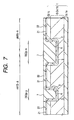
- FIG. 7 is a fragmentary cross-sectional view of a substrate illustrating a step in the method of manufacture of the semiconductor integrated circuit device according to Embodiment 1 of the present invention.
- FIG. 8 is a fragmentary cross-sectional view of a substrate illustrating a step in the method of manufacture of the semiconductor integrated circuit device according to Embodiment 1 of the present invention.
- FIG. 9 is a fragmentary cross-sectional view of a substrate illustrating a step in the method of manufacture of the semiconductor integrated circuit device according to Embodiment 1 of the present invention.
- FIG. 10 is a fragmentary cross-sectional view of a substrate illustrating a step in the method of manufacture of the semiconductor integrated circuit device according to Embodiment 1 of the present invention.
- FIG. 11 is a fragmentary cross-sectional view of a substrate illustrating a step in the method of manufacture of the semiconductor integrated circuit device according to Embodiment 1 of the present invention
- FIG. 12 is a fragmentary cross-sectional view of a substrate illustrating a step in the method of manufacture of the semiconductor integrated circuit device according to Embodiment 1 of the present invention
- FIG. 13 is a fragmentary cross-sectional view of a substrate illustrating a step in the method of manufacture of the semiconductor integrated circuit device according to Embodiment 1 of the present invention
- FIG. 14 is a fragmentary plan view of a substrate illustrating a step in the method of manufacture of the semiconductor integrated circuit device according to Embodiment 1 of the present invention.
- FIG. 15 is a fragmentary cross-sectional view of a substrate of the semiconductor integrated circuit device illustrating an advantage of Embodiment 1 of the present invention
- FIG. 16 is a fragmentary cross-sectional view of a substrate of the semiconductor integrated circuit device illustrating another advantage of Embodiment 1 of the present invention.
- FIG. 17 is a fragmentary cross-sectional view taken along line A—A in FIG. 18 ;
- FIG. 18 is a fragmentary plan view of a substrate of the semiconductor integrated circuit device illustrating a further advantage of Embodiment 1 of the present invention.
- FIG. 19 is a fragmentary plan view of a substrate of the semiconductor integrated circuit device similar to that of FIG. 18 ;
- FIG. 20 is a fragmentary cross-sectional view of a substrate illustrating a step in the method of manufacture of a semiconductor integrated circuit device according to Embodiment 2 of the present invention
- FIG. 21 is a fragmentary cross-sectional view of a substrate illustrating a step in the method of manufacture of the semiconductor integrated circuit device according to Embodiment 2 of the present invention.
- FIG. 22 is a fragmentary cross-sectional view of a substrate illustrating a step in the method of manufacture of the semiconductor integrated circuit device according to Embodiment 2 of the present invention.
- FIG. 23 is a fragmentary cross-sectional view of a substrate illustrating a step in the method of manufacture of the semiconductor integrated circuit device according to Embodiment 2 of the present invention.
- FIG. 24 is a fragmentary cross-sectional view of a substrate illustrating method of manufacture of a semiconductor integrated circuit device according to Embodiment 3 of the present invention.
- FIG. 25 is a fragmentary cross-sectional view of a substrate illustrating a step in the method of manufacture of the semiconductor integrated circuit device according to Embodiment 3 of the present invention.
- FIG. 26 is a fragmentary cross-sectional view of a substrate illustrating a step in the method of manufacture of the semiconductor integrated circuit device according to Embodiment 3 of the present invention.
- FIG. 27 is a fragmentary cross-sectional view of a substrate illustrating a step in the method of manufacture of the semiconductor integrated circuit device according to Embodiment 3 of the present invention.
- FIG. 28 is a fragmentary cross-sectional view of a substrate illustrating a step in the method of manufacture of the semiconductor integrated circuit device according to Embodiment 3 of the present invention.
- FIG. 29 is a fragmentary cross-sectional view of a substrate illustrating a step in the method of manufacture of a semiconductor integrated circuit device according to Embodiment 4 of the present invention.
- FIG. 30 is a fragmentary cross-sectional view of a substrate illustrating a step in the method of manufacture of the semiconductor integrated circuit device according to Embodiment 4 of the present invention.
- FIG. 31 is a fragmentary cross-sectional view of a substrate illustrating a step in the method of manufacture of the semiconductor integrated circuit device according to Embodiment 4 of the present invention.
- FIG. 32 is a fragmentary cross-sectional view of a substrate illustrating a step in the method of manufacture of the semiconductor integrated circuit device according to Embodiment 4 of the present invention.
- FIG. 33 is a fragmentary cross-sectional view of a substrate illustrating a step in the method of manufacture the semiconductor integrated circuit device according to Embodiment 4 of the present invention.
- a semiconductor integrated circuit device according to this Embodiment will be described in the sequence of its manufacturing steps.
- FIGS. 1 to 13 are each a fragmentary cross-sectional view of a substrate illustrating a respective step in the method of manufacture of a semiconductor integrated circuit device according to this Embodiment.
- FIG. 14 is a fragmentary plan view of the substrate, and each cross-sectional view is a view taken along a line A—A of the plan view.
- the region nMIS-A is the region where an n-channel type MISFET is formed, while the region pMIS-A is the region where a p-channel type MISFET is formed.
- a semiconductor substrate (which will hereinafter be called “substrate”, simply) is formed, having, as illustrated in FIG. 1 , a single crystal silicon (Si) layer 1 a , an SiGe (silicon germanium) layer 1 b , and a single crystal Si layer 1 c epitaxially grown thereover.
- Si silicon
- SiGe silicon germanium
- This substrate 1 is formed as follows. First, a SiGe layer 1 b of about 5 ⁇ m thick is formed over the surface of the single crystal Si substrate 1 a by epitaxial growth while using Si and Ge at a composition ratio (Si:Ge) of, for example, 0.8:0.2. Then, a Si layer 1 c of about 0.02 ⁇ m is formed over the SiGe layer 1 b by epitaxial growth.
- a tensile stress is applied to the Si layer 1 c of the substrate 1 .
- the lattice spacing of the SiGe layer 1 b is wider than that of the single crystal Si so that the Si layer grown over the SiGe layer 1 b has a widened lattice spacing, influenced by that of the SiGe layer. Although this widening of the lattice spacing is relaxed as the growth of the film proceeds, a tensile stress is applied to the Si layer 1 c , and the mobility of the carriers increases when the lattice spacing of the Si layer is wider than that of the general Si crystal over the surface of the substrate.
- This substrate 1 is called a “strained substrate”, while the Si layer 1 c is called a “strained layer”.
- a shallow groove isolation SGI serving as an element isolation, is then formed in the substrate 1 .
- This shallow groove isolation SGI is formed, as illustrated in FIG. 2 , by forming a silicon oxide film 21 that is about 10 nm thick over the surface of the substrate 1 , and, then, depositing a silicon nitride film 22 of about 150 nm over the silicon oxide film.
- the silicon nitride film 22 and silicon oxide film 21 are removed from the element isolation regions (ISOp-p, ISOp-n) of the substrate 1 .
- the substrate 1 is etched, using the silicon nitride film 22 as a mask, to form a groove 2 .
- the groove 2 must have a depth of about 300 nm in this case in order to maintain element isolating properties. This groove 2 extends through the Si layer 1 c and reaches the SiGe layer 1 b . The bottom of the groove 2 exists in the SiGe layer 1 b.
- the Si layer 1 c and SiGe layer 1 b are exposed from the side walls of the groove 2 , while the SiGe layer 1 b is exposed from the bottom of the groove 2 .
- Reduction for example, heat treatment in a hydrogen atmosphere, is then conducted to remove a natural oxide film from the surface of the groove 2 .
- single crystal Si is epitaxially grown over the Si layer 1 c and SiGe layer 1 b of the side walls of the groove and over the SiGe layer 1 b of the bottom of the groove 2 , whereby a single crystal Si film 3 that is about 20 nm thick is formed.
- single crystal Si grows not only horizontally, but also vertically, relative to the surface of the substrate, which means that there is growth of single crystal Si to form a protrusion, at the upper portion of the side walls of the groove, from the surface of the substrate 1 .
- an Si oxide film (thermal oxide film) 6 is to be formed by oxidizing the surface of the Si film 3 on the inside wall of the groove 2 .
- the silicon oxide film 21 is selectively etched to cause it to retreat from the side walls of the groove, as illustrated in FIG. 4 .
- the surface of the Si film 3 on the inside wall of the groove 2 is oxidized to form an Si oxide film (thermal oxide film) 6 .
- This Si oxide film 6 is formed for the purpose of (1) suppressing generation of crystal defects which will otherwise occur owing to stress concentration to a corner portion (a 1 ) on the bottom of the groove by rounding the Si oxide film 6 on the corner portion; and (2) suppressing fluctuations in the characteristics of a semiconductor element, which will otherwise occur owing to electric field concentration to a corner portion (a 2 ) at the upper portion of the side walls of the groove, by rounding the Si oxide film 6 on the corner portion.
- the Si oxide film (thermal oxide film) 6 which is capable of suppressing the interface state density even if they are brought into contact, is interposed (3) for the purpose of keeping an increase in interface state density small.
- oxidation is conducted after the silicon oxide film 2 has retreated from the side wall portions of the groove 2 (FIG. 4 ). This makes it possible to enlarge the bird's beak and ease the angle of the corner, whereby the electric field concentration can be relaxed further.
- oxidation of Si forms an Si oxide film having twice as much volume as that of Si
- oxidation of 10 nm of the Si film 3 having a thickness of 20 nm
- a silicon oxide film 7 is deposited as an insulating film by CVD (Chemical Vapor Deposition) over the substrate 1 including the inside (over the Si oxide film 6 ) of the groove 2 .
- This silicon oxide film can be formed, for example, by CVD using tetraethoxysilane (Si(OC 2 H 5 ) 4 ) and ozone (O 3 ) as raw materials.
- Such a film is referred to as an “ozone TEOS (O 3 -TEOS) film”.
- the O 3 -TEOS film is then heat treated (densified) to remove impurities therefrom to obtain a dense film.
- the method of formation of the silicon oxide film 7 is not limited to the above-described one, but HDP (High Density Plasma) CVD can be employed instead. This method does not need densification.
- the silicon oxide film 7 is polished, for example, by CMP (Chemical Mechanical Polishing) until the silicon nitride film 22 is exposed therefrom, whereby the surface of the silicon oxide film is planarized.
- CMP Chemical Mechanical Polishing
- the silicon nitride film 22 is removed.
- the Si film 3 on the inside wall of the groove 2 and a shallow groove isolation SGI, made of the Si oxide film 6 and silicon oxide film 7 are completed.
- a region surrounded by this shallow groove isolation SGI becomes an element formation region (refer to FIG. 14 ).
- the silicon oxide film 7 on the surface of the shallow groove isolation SGI protrudes from the surface of the substrate 1 , but this protrusion of the shallow groove isolation SGI disappears gradually in the subsequent steps, such as cleaning of the substrate and removal of the thermal oxide film.
- the width H 2 of the shallow groove isolation on the boundary between an n channel type MISFET formation region (nMIS-A) and a p channel type MISFET formation region (pMIS-A) is greater than the width H 1 of the shallow groove isolation in the n-channel MISFET formation region (nMIS-A).
- the shallow groove isolation having a width H 1 will be an isolation in a p type well 4 p , which will be described later, so that it is referred to as an “intra-well isolation (ISOp-p)”, while that having the width H 2 will be an isolation between the p type well 4 p and an n type well 4 n , so that it is called a “well-well isolation (ISOn-p)”.
- the width H 1 of the intra-well isolation is about 0.2 ⁇ m, while the width H 2 of the well-well isolation is about 0.4 ⁇ m.
- boron is ion-implanted as a p type impurity at a dose of about 2 ⁇ 10 13 cm ⁇ 2 in the n channel MISFET formation region (nMIS-A) of the substrate 1 .
- nMIS-A n channel MISFET formation region
- phosphorus is ion-implanted as an n type impurity at a dose of about 2 ⁇ 10 13 cm ⁇ 2 .
- Heat treatment is then conducted to diffuse these impurities, whereby n type well 4 n and p type well 4 p are formed.
- the n type well 4 n and p type well 4 p each has a depth of about 450 nm, and the n type well 4 n and p type well 4 p each has a bottom in the SiGe layer 1 b.
- the bottom of the n type well 4 n and p type well 4 p exist at a position deeper than the bottom of the shallow groove isolation SGI. In this case, the well has a maximum concentration of about 2 ⁇ 10 18 cm ⁇ 3 .
- a gate oxide film (gate insulating film) 8 that is about 2 nm thick is formed on the surface of each of the p type well 4 p and n type well 4 n by thermal oxidation.
- a low resistance polycrystalline silicon film 9 that is about 150 nm thick is formed as a conductive film by CVD. Then, using an unillustrated film as a mask, the polycrystalline silicon film 9 is etched to form a gate electrode G.
- a gate electrode G is also formed over the shallow groove isolations SGI (ISOp-p, ISOp-n).
- a gate electrode over another un-illustrated element formation region may extend even over the shallow groove isolation SGI.
- the polycrystalline silicon film ( 9 ), which is in the same layer with the gate electrode G, may be formed over the shallow groove isolation as an interconnect or resistor.
- arsenic (As) is implanted as an n type impurity to both sides of the gate electrode G of the p type well 4 p , whereby n ⁇ type semiconductor regions 11 are formed.
- a p type impurity is implanted to both sides of the gate electrode G of the n type well 4 n , whereby p ⁇ type semiconductor regions 12 are formed.
- a silicon nitride film that is about 70 nm thick is deposited over the substrate 1 by CVD, followed by anisotropic etching to form side wall spacers 13 that are about 50 nm thick over the side walls of the gate electrode G.
- n + type semiconductor regions 14 and p + type semiconductor regions 15 are formed.
- n + type semiconductor regions 14 and p + type semiconductor regions 15 extend even to the SiGe layer 1 b . These regions may have a bottom in the Si layer 1 c by reducing their depth. To enlarge the tensile stress of the Si layer 1 c , however, a decrease in the thickness of the Si layer 1 c as much as possible is desired. In such a case, the n + type semiconductor regions 14 and p + type semiconductor regions 15 (source and drain) will extend to the SiGe layer 1 b.
- FIG. 14 is a fragmentary cross-sectional view of a substrate of the semiconductor integrated circuit device according to this Embodiment.
- the MISFET is formed over the strained substrate 1 , so that the mobility of electrons in a channel region can be improved, which results in an improvement in the current driving capacity of the MISFET, particularly, the current driving capacity of the n channel type MISFET.
- the Si film 3 is formed between the shallow groove isolation SGI and the SiGe layer 1 b so that the interface state density on the interface between the shallow groove isolation SGI and Si film 3 can be reduced, leading to a reduction in the leakage current flowing via the interface.
- an Si oxide film 6 a and an SiGe oxide film 6 b by directly oxidizing the side walls and bottom of the groove 2 .
- the SiGe oxide film 6 b has an interface state density of about one order of magnitude greater than that of the Si oxide film, direct oxidization of the inside wall of the groove 2 is insufficient as a countermeasure against leakage current.
- electrons become apt to be trapped around the shallow groove isolation (SiGe oxide film 6 b ), which causes a leakage current to flow along the wall of the shallow groove isolation.
- no SiGe oxide film 6 b exists on the interface between the shallow groove isolation SGI and the SiGe layer 1 b , so that the leakage current can be reduced.
- contact between the CVD insulating film ( 7 ) and the substrate can be avoided by the Si oxide film 6 , which is formed by oxidizing the Si film 3 , which has been formed over the inside wall of the groove 2 , whereby an interface state density between them can be reduced.
- the Si oxide film 6 is oxidized further by the heat treatment after formation of the Si oxide film 6 , for example, densification of the O 3 -TEOS film ( 7 ) or activation of impurities constituting the source and drain ( 14 and 15 ), the remaining Si film 3 is oxidized as needed, whereby the oxidation of the SiGe layer 1 b can be prevented. This leads to suppression of a rise in the interface state density, which will otherwise occur by the existence of the SiGe oxide film.
- the well has a relatively high concentration (for example, 1 ⁇ 10 18 cm ⁇ 3 or greater) or a conductive film (gate electrode) is formed over the shallow groove isolation, electrons are apt to be trapped at the periphery of the shallow groove isolation SGI, as illustrated in FIG. 16 .
- a relatively high concentration for example, 1 ⁇ 10 18 cm ⁇ 3 or greater
- a conductive film gate electrode
- a parasitic MOS transistor is formed by the conductive film (gate electrode) and shallow groove isolation SGI.
- a potential is applied to the conductive film, electrons are accumulated on the outside wall of the shallow groove isolation, and application of a potential exceeding a threshold potential (Vt) of the parasitic MOS to the conductive film turns the parasitic MOS transistor on.
- Vt threshold potential
- This Embodiment is therefore more effective when used in such a case (where the well has a relatively high concentration, or the gate electrode is formed over the shallow groove isolation).
- FIG. 18 is a fragmentary plan view of the substrate of the semiconductor integrated circuit device illustrated in FIG. 17 and FIG. 17 corresponds to a cross-section taken along a line A—A of FIG. 18 .
- the shallow groove isolation SGI tends to be shallow, reflecting the miniaturization of the element. This is partly because, when a pattern area becomes small, the aspect ratio (depth of a groove/pattern width) increases, resulting in a deterioration in the embedding property of an insulating film.
- this Embodiment can be used suitably.
- a metal film such as a Co (cobalt) film
- Co cobalt
- a metal film is deposited over the substrate 1 , followed by heat treatment to cause a silicidation reaction at the contact portion of the metal film with each of the gate electrode G and substrate 1 , whereby CoSi 2 (cobalt silicide film) 17 is formed in self alignment.
- an unreacted portion of the Co film is removed, followed by heat treatment.
- a silicon oxide film 19 is then deposited by CVD over the substrate 1 as an interlayer insulating film, and it is planarized at the surface thereof as needed.
- the silicon oxide film 19 deposited over the source and drain ( 15 and 14 ) and gate electrode of the MISFETS (Qn and Qp), are etched to form contact holes C 1 .
- the contact hole over the gate electrode is not illustrated.
- W tungsten film
- a W film for example, serving as a conductive film, is deposited, followed by patterning into a desired shape to form a first-level interconnect M 1 .
- a multilevel interconnect can be formed, but illustration and detailed description of the formation thereof are omitted.
- a protective film having an opening at the pad portion is formed over the uppermost-level interconnect and the substrate 1 in the form of a wafer is diced into a plurality of chips.
- the pad portion and external lead are connected by a bump electrode or wire, and, if necessary, the chip is sealed at the periphery thereof with a resin, whereby a semiconductor integrated circuit device is completed.
- the Si film 3 remains.
- Embodiment 1 a single crystal Si film formed by epitaxial growth is used as the Si film 3 .
- a polycrystalline silicon film is usable.
- FIGS. 20 to 23 are fragmentary cross-sectional views of a substrate, each illustrating the method of manufacture of the semiconductor integrated circuit device according to this Embodiment. Steps up to the formation of the groove 2 are similar to those described in connection with Embodiment 1, based on FIGS. 1 and 2 , so that a further description thereof is omitted.
- a polycrystalline silicon film 203 that is about 20 nm thick is deposited by CVD over the strained substrate 1 having the groove 2 formed therein.
- Numeral 21 indicates a silicon nitride film, while numeral 22 indicates a silicon nitride film.
- the surface of the polycrystalline silicon film 203 is oxidized to form an Si oxide film (thermal oxide film) 206 .
- a portion of the Si film 203 corresponding to a predetermined thickness from the surface thereof is oxidized.
- an unoxidized portion of the Si film 203 remains.
- the Si film 203 having a thickness of 20 nm the upper 10 nm portion is oxidized to form an Si oxide film 206 that is about 20 nm thick, and the lower 10 nm portion of the Si film 203 is left unoxidized.
- This oxidation rounds the Si oxide film 206 existing at a corner portion (a 1 ) on the bottom of the groove. As a result, generation of crystal defects owing to stress concentration at the corner portion can be suppressed.
- a silicon oxide film 7 is deposited as an insulating film by CVD over the substrate 1 (over the Si oxide film 206 ), including the inside of the groove 2 .
- This silicon oxide film is, for example, an O 3 -TEOS film, as described in Embodiment 1.
- the O 3 -TEOS film is then heat treated in an oxygen atmosphere in order to remove impurities in the film and densify the film.
- the silicon oxide film 7 is polished, for example, by CMP until the silicon nitride film 22 appears, whereby the surface of the silicon oxide film is planarized. Then, the silicon nitride film is removed.
- the intra-well isolation has a width H 1 of, for example, about 0.2 ⁇ m.
- the width H 2 of the well-well isolation (ISOn-p) is greater than the width H 1 and is, for example, about 0.4 ⁇ m.
- MISFETs Qn and Qp
- Subsequent formation steps are similar to those described in connection with Embodiment 1, based on FIGS. 9 to 14 , so a further explanation thereof is omitted.
- Embodiment also brings about similar effects to those of Embodiment 1.
- the interface state density between the shallow groove isolation SGI and substrate 1 is considered to be smaller via the single crystal Si film of Embodiment 1, than it is via the polycrystalline silicon film.
- the CVD insulating film ( 7 ) was deposited directly over the Si oxide film ( 6 or 206 ), but it is possible to dispose therebetween a silicon nitride film.
- FIGS. 24 to 28 are each a fragmentary cross-sectional view of a substrate illustrating the method of manufacture of the semiconductor integrated circuit device of this Embodiment. Steps up to the formation of the Si oxide film 6 are similar to those of Embodiment 1, as described with reference to FIGS. 1 to 5 , so that an explanation of them will be omitted. As described in detail in connection with Embodiment 1 (FIG. 5 ), the Si oxide film 6 existing at the corner portion (a 1 ) on the bottom of the groove or that existing at the corner portion (a 2 ) at the upper portion of the side walls of the groove are rounded, however this is illustrated in FIG. 24 only simply.
- a silicon nitride film 306 that is about 10 nm thick is deposited using CVD, as illustrated in FIG. 24 .
- Numeral 21 indicates a silicon oxide film and numeral 22 indicates a silicon nitride film.
- a silicon oxide film 7 is deposited as an insulating film by CVD.
- This silicon oxide film is, for example, an O 3 -TEOS film, as explained in connection with Embodiment 1. Then, the O 3 -TEOS film is heat treated in an oxygen atmosphere to remove impurities therefrom and to densify the film.
- the silicon oxide film 7 is polished, for example, by CMP until the silicon nitride film 22 is exposed and the surface of the silicon oxide film is planarized. Then, the silicon nitride film 22 is removed.
- the intra-well isolation has a width H 1 of, for example, about 0.2 ⁇ m.
- the width H 2 of the well-well isolation (ISOn-p) is greater than the width H 1 and is, for example, about 0.4 ⁇ m.
- MISFETs (Qn, Qp) are then formed. Subsequent formation steps are similar to those as described in connection with Embodiment 1, based on FIGS. 9 to 14 , so a detailed explanation thereof is omitted.
- This embodiment brings about effects similar to those of Embodiment 1.
- the silicon nitride film 306 is formed over the Si oxide film 6 , the progress of oxidation of the Si oxide film 6 , which will otherwise occur owing to heat treatment after the formation of the Si oxide film 6 , for example, densification of the O 3 -TEOS film ( 7 ), as explained in detail in connection with Embodiment 1, or activation of impurities constituting the source and drain ( 14 and 15 ), can be suppressed. This makes it possible to suppress oxidation of the Si film 3 , thereby leaving the Si film 3 without failure.
- volumetric expansion occurs, whereby stress is applied to the shallow groove isolation and crystal defects tend to occur. Formation of the silicon nitride film 306 reduces the influence of the stress, thereby preventing the generation of crystal defects.
- the silicon nitride film 306 may be anisotropically etched, as illustrated in FIG. 27 , to leave the silicon nitride film 306 a only on the side wall portions of the groove 2 .
- the Si oxide film 6 existing at the corner portions (a 1 and a 2 ) of the groove is rounded, but such portions are illustrated only simply in FIG. 27 .
- the silicon oxide film 7 is polished until the silicon nitride film 22 is exposed, whereby the surface of the silicon oxide film is planarized (FIG. 28 ). Then, the silicon nitride film 22 is removed.
- FIGS. 29 to 33 are fragmentary cross-sectional views of the substrate illustrating the method of manufacture of the semiconductor integrated circuit device of this Embodiment. Steps up to the formation of the groove 2 are similar to those of Embodiment 1, as described with reference to FIGS. 1 and 2 , so that a description thereof is omitted.
- the surface of the strained substrate 1 is oxidized to form an Si oxide film 402 a and an SiGe oxide film 402 b , as illustrated in FIG. 29 .
- These oxide films each has a thickness of about 20 nm.
- only the SiGe oxide film 402 b is selectively removed using, for example, H 2 O (water), while the Si oxide film 402 b is left.
- H 2 O water
- the SiGe oxide film 402 b is etched under the conditions of a high selectivity relative to the Si oxide film.
- the SiGe oxide film is water soluble, so that it can be removed easily.
- single crystal Si is epitaxially grown over the exposed SiGe layer 1 b to form an Si film 403 that is about 20 nm thick. Growth of Si does not occur over the Si layer 1 c on the side walls of the groove, because the Si oxide film 402 a remains on the Si layer.
- the surface of the Si film 403 over the inside wall of the groove 2 is oxidized to form an Si oxide film (thermal oxide film) 406 .
- a silicon oxide film 7 is deposited by CVD as an insulating film over the substrate 1 , including the inside of the groove 2 (over the Si oxide films 402 a and 406 ).
- This silicon oxide film is, for example, an O 3 -TEOS film, as described in Embodiment 1.
- the O 3 -TEOS film is then heat treated in an oxygen atmosphere in order to remove impurities in the film and densify the film.
- the silicon oxide film 7 is then polished, for example, by CMP until the silicon nitride film 22 appears, whereby the surface of the silicon oxide film is planarized. Then, the silicon nitride film 22 is removed.
- the intra-well isolation has a width H 1 of, for example, about 0.2 ⁇ m.
- the width H 2 of the well-well isolation (ISOn-p) is greater than the width H 1 and is, for example, about 0.4 ⁇ m.
- MISFETs (Qn, Qp) are then formed. Subsequent formation steps are similar to those as described in connection with Embodiment 1, based on FIGS. 9 to 14 , so a detailed explanation thereof is omitted.
- Embodiment also brings about effects similar to those of Embodiment 1.
- Si is epitaxially grown only over the SiGe layer 1 b inside of the groove, using the Si oxide film 402 a as a mask, so that in the Si film 403 , no boundary exists between a portion grown from the Si layer 1 c and a portion grown from the SiGe layer 1 b (refer to FIG. 3 ). This brings about an improvement in the film quality.
- This Embodiment can avoid formation of a surface discontinuity in the Si film 403 , thereby reducing the crystal defects of the remaining Si film 403 .
- Embodiment 3 may be applied to this Embodiment; in other words, a silicon nitride film may be formed over the Si oxide film 406 of this Embodiment.
- the invention was applied to the case where a MISFET is formed, but the invention is applicable also to semiconductor integrated circuit devices having other semiconductor device configurations, for example, a bipolar transistor, and a current channel and element isolation on the surface of the substrate.
- a shallow groove isolation is formed of a groove, which is formed in an isolation region of a strained substrate having an SiGe layer and a first Si layer formed thereover by epitaxial growth, and an insulating film inside of the groove. Since a second Si layer is formed between the shallow groove isolation, which penetrates the first Si layer and has its bottom in the SiGe layer and the SiGe layer, the element isolating properties of the strained substrate can be improved. In addition, the characteristics of a semiconductor integrated circuit formed over the main surface of the strained substrate can be improved. Moreover, the yield of the device can be improved.
- the leakage current via the shallow groove isolation can be reduced, leading to an improvement in element isolating properties.
Landscapes
- Element Separation (AREA)
- Metal-Oxide And Bipolar Metal-Oxide Semiconductor Integrated Circuits (AREA)
- Insulated Gate Type Field-Effect Transistor (AREA)
Applications Claiming Priority (2)
| Application Number | Priority Date | Filing Date | Title |
|---|---|---|---|
| JP2002-184292 | 2002-06-25 | ||
| JP2002184292A JP4421811B2 (ja) | 2002-06-25 | 2002-06-25 | 半導体集積回路装置およびその製造方法 |
Publications (2)
| Publication Number | Publication Date |
|---|---|
| US20040009636A1 US20040009636A1 (en) | 2004-01-15 |
| US6847093B2 true US6847093B2 (en) | 2005-01-25 |
Family
ID=30112248
Family Applications (1)
| Application Number | Title | Priority Date | Filing Date |
|---|---|---|---|
| US10/602,697 Expired - Fee Related US6847093B2 (en) | 2002-06-25 | 2003-06-25 | Semiconductor integrated circuit device |
Country Status (4)
| Country | Link |
|---|---|
| US (1) | US6847093B2 (https=) |
| JP (1) | JP4421811B2 (https=) |
| KR (1) | KR20040002665A (https=) |
| TW (1) | TW200403802A (https=) |
Cited By (8)
| Publication number | Priority date | Publication date | Assignee | Title |
|---|---|---|---|---|
| US20050194585A1 (en) * | 2004-03-05 | 2005-09-08 | Kabushiki Kaisha Toshiba | Field effect transistor and a method for manufacturing the same |
| US20050282353A1 (en) * | 2004-06-17 | 2005-12-22 | Texas Instruments, Incorporated | Trench isolation structure and a method of manufacture therefor |
| US20060292762A1 (en) * | 2005-06-22 | 2006-12-28 | Epion Corporation | Replacement gate field effect transistor with germanium or SiGe channel and manufacturing method for same using gas-cluster ion irradiation |
| US20080087981A1 (en) * | 2006-10-02 | 2008-04-17 | Kabushiki Kaisha Toshiba | Semiconductor device and method of fabricating the same |
| US20080087892A1 (en) * | 2006-03-28 | 2008-04-17 | Chih-Hao Wang | High Performance Transistor with a Highly Stressed Channel |
| US20090090935A1 (en) * | 2005-01-21 | 2009-04-09 | Taiwan Semiconductor Manufacturing Company Ltd. | High Performance CMOS Device Design |
| US20110195572A1 (en) * | 2007-03-30 | 2011-08-11 | Elpida Memory, Inc. | Chip-stacked semiconductor device and manufacturing method thereof |
| US20120091505A1 (en) * | 2010-10-14 | 2012-04-19 | Kabushiki Kaisha Toshiba | Semiconductor device |
Families Citing this family (17)
| Publication number | Priority date | Publication date | Assignee | Title |
|---|---|---|---|---|
| JP4750342B2 (ja) * | 2002-07-03 | 2011-08-17 | ルネサスエレクトロニクス株式会社 | Mos−fetおよびその製造方法、並びに半導体装置 |
| JP4368095B2 (ja) * | 2002-08-21 | 2009-11-18 | 富士通マイクロエレクトロニクス株式会社 | 半導体装置及びその製造方法 |
| US20040164373A1 (en) * | 2003-02-25 | 2004-08-26 | Koester Steven John | Shallow trench isolation structure for strained Si on SiGe |
| US7238985B2 (en) * | 2003-08-13 | 2007-07-03 | International Rectifier Corporation | Trench type mosgated device with strained layer on trench sidewall |
| JP2005197405A (ja) * | 2004-01-06 | 2005-07-21 | Toshiba Corp | 半導体装置とその製造方法 |
| US7462549B2 (en) * | 2004-01-12 | 2008-12-09 | Advanced Micro Devices, Inc. | Shallow trench isolation process and structure with minimized strained silicon consumption |
| KR100620707B1 (ko) * | 2004-12-31 | 2006-09-13 | 동부일렉트로닉스 주식회사 | 반도체 소자의 sti 형성 방법 |
| US9698044B2 (en) * | 2011-12-01 | 2017-07-04 | Taiwan Semiconductor Manufacturing Company, Ltd. | Localized carrier lifetime reduction |
| KR101831936B1 (ko) * | 2011-12-22 | 2018-02-26 | 삼성전자주식회사 | 박막 형성 방법 및 이를 이용한 반도체 소자의 제조 방법 |
| US8828851B2 (en) * | 2012-02-01 | 2014-09-09 | Stmicroeletronics, Inc. | Method to enable the formation of silicon germanium channel of FDSOI devices for PFET threshold voltage engineering |
| US9209066B2 (en) * | 2013-03-01 | 2015-12-08 | Taiwan Semiconductor Manufacturing Company, Ltd. | Isolation structure of semiconductor device |
| US9099324B2 (en) * | 2013-10-24 | 2015-08-04 | Taiwan Semiconductor Manufacturing Co., Ltd. | Semiconductor device with trench isolation |
| US9960273B2 (en) * | 2015-11-16 | 2018-05-01 | Taiwan Semiconductor Manufacturing Company, Ltd. | Integrated circuit structure with substrate isolation and un-doped channel |
| DE102017126435B4 (de) * | 2017-08-31 | 2022-07-28 | Taiwan Semiconductor Manufacturing Company, Ltd. | Fin-feldeffekttransistorvorrichtung und verfahren |
| US10497577B2 (en) | 2017-08-31 | 2019-12-03 | Taiwan Semiconductor Manufacturing Company, Ltd. | Fin field-effect transistor device and method |
| US11594597B2 (en) | 2019-10-25 | 2023-02-28 | Taiwan Semiconductor Manufacturing Company, Ltd. | Selective polysilicon growth for deep trench polysilicon isolation structure |
| US20240429166A1 (en) * | 2023-06-23 | 2024-12-26 | International Business Machines Corporation | Trench isolation structures for backside contacts |
Citations (2)
| Publication number | Priority date | Publication date | Assignee | Title |
|---|---|---|---|---|
| US6274894B1 (en) * | 1999-08-17 | 2001-08-14 | Advanced Micro Devices, Inc. | Low-bandgap source and drain formation for short-channel MOS transistors |
| US6570217B1 (en) * | 1998-04-24 | 2003-05-27 | Kabushiki Kaisha Toshiba | Semiconductor device and method of manufacturing the same |
Family Cites Families (3)
| Publication number | Priority date | Publication date | Assignee | Title |
|---|---|---|---|---|
| DE4102888A1 (de) * | 1990-01-31 | 1991-08-01 | Toshiba Kawasaki Kk | Verfahren zur herstellung eines miniaturisierten heterouebergang-bipolartransistors |
| JP2980497B2 (ja) * | 1993-11-15 | 1999-11-22 | 株式会社東芝 | 誘電体分離型バイポーラトランジスタの製造方法 |
| US6399970B2 (en) * | 1996-09-17 | 2002-06-04 | Matsushita Electric Industrial Co., Ltd. | FET having a Si/SiGeC heterojunction channel |
-
2002
- 2002-06-25 JP JP2002184292A patent/JP4421811B2/ja not_active Expired - Fee Related
-
2003
- 2003-06-09 TW TW092115541A patent/TW200403802A/zh unknown
- 2003-06-24 KR KR1020030041050A patent/KR20040002665A/ko not_active Withdrawn
- 2003-06-25 US US10/602,697 patent/US6847093B2/en not_active Expired - Fee Related
Patent Citations (2)
| Publication number | Priority date | Publication date | Assignee | Title |
|---|---|---|---|---|
| US6570217B1 (en) * | 1998-04-24 | 2003-05-27 | Kabushiki Kaisha Toshiba | Semiconductor device and method of manufacturing the same |
| US6274894B1 (en) * | 1999-08-17 | 2001-08-14 | Advanced Micro Devices, Inc. | Low-bandgap source and drain formation for short-channel MOS transistors |
Non-Patent Citations (1)
| Title |
|---|
| K. Rim, et al., "Strained Si NMOSFETs for High Performance CMOS Technology, 2001, Symposium on VLSI Technology digest of Technical Papers", pp. 59-60. |
Cited By (17)
| Publication number | Priority date | Publication date | Assignee | Title |
|---|---|---|---|---|
| US20050194585A1 (en) * | 2004-03-05 | 2005-09-08 | Kabushiki Kaisha Toshiba | Field effect transistor and a method for manufacturing the same |
| US20050282353A1 (en) * | 2004-06-17 | 2005-12-22 | Texas Instruments, Incorporated | Trench isolation structure and a method of manufacture therefor |
| US7371658B2 (en) * | 2004-06-17 | 2008-05-13 | Texas Instruments Incorporated | Trench isolation structure and a method of manufacture therefor |
| US20080185675A1 (en) * | 2004-06-17 | 2008-08-07 | Texas Instruments Incorporated | Trench Isolation Structure and a Method of Manufacture Therefor |
| US8507951B2 (en) | 2005-01-21 | 2013-08-13 | Taiwan Semiconductor Manufacturing Company, Ltd. | High performance CMOS device design |
| US20090090935A1 (en) * | 2005-01-21 | 2009-04-09 | Taiwan Semiconductor Manufacturing Company Ltd. | High Performance CMOS Device Design |
| US9711413B2 (en) | 2005-01-21 | 2017-07-18 | Taiwan Semiconductor Manufacturing Company, Ltd. | High performance CMOS device design |
| US9159629B2 (en) | 2005-01-21 | 2015-10-13 | Taiwan Semiconductor Manufacturing Company Ltd. | High performance CMOS device design |
| US20060292762A1 (en) * | 2005-06-22 | 2006-12-28 | Epion Corporation | Replacement gate field effect transistor with germanium or SiGe channel and manufacturing method for same using gas-cluster ion irradiation |
| WO2007002130A3 (en) * | 2005-06-22 | 2007-10-04 | Epion Corp | Replacement gate field effect transistor with germanium or sige channel and manufacturing method for same using gas-cluster ion irradiation |
| US20080087892A1 (en) * | 2006-03-28 | 2008-04-17 | Chih-Hao Wang | High Performance Transistor with a Highly Stressed Channel |
| US7649233B2 (en) * | 2006-03-28 | 2010-01-19 | Taiwan Semiconductor Manufacturing Company, Ltd. | High performance transistor with a highly stressed channel |
| US20080087981A1 (en) * | 2006-10-02 | 2008-04-17 | Kabushiki Kaisha Toshiba | Semiconductor device and method of fabricating the same |
| US8722502B2 (en) | 2007-03-30 | 2014-05-13 | Shiro Uchiyama | Chip-stacked semiconductor device and manufacturing method thereof |
| US20110195572A1 (en) * | 2007-03-30 | 2011-08-11 | Elpida Memory, Inc. | Chip-stacked semiconductor device and manufacturing method thereof |
| US8390028B2 (en) * | 2010-10-14 | 2013-03-05 | Kabushiki Kaisha Toshiba | Semiconductor device with epitaxial crystal layer embedded within susbstrate of dummy pattern region |
| US20120091505A1 (en) * | 2010-10-14 | 2012-04-19 | Kabushiki Kaisha Toshiba | Semiconductor device |
Also Published As
| Publication number | Publication date |
|---|---|
| KR20040002665A (ko) | 2004-01-07 |
| JP4421811B2 (ja) | 2010-02-24 |
| TWI297192B (https=) | 2008-05-21 |
| JP2004031559A (ja) | 2004-01-29 |
| US20040009636A1 (en) | 2004-01-15 |
| TW200403802A (en) | 2004-03-01 |
Similar Documents
| Publication | Publication Date | Title |
|---|---|---|
| US6847093B2 (en) | Semiconductor integrated circuit device | |
| CN100539151C (zh) | 半导体装置及半导体集成电路装置 | |
| US6221735B1 (en) | Method for eliminating stress induced dislocations in CMOS devices | |
| CN100565878C (zh) | 半导体装置 | |
| KR0165457B1 (ko) | 트렌치 소자분리 방법 | |
| JP3559723B2 (ja) | 半導体装置の製造方法 | |
| US6649462B2 (en) | Semiconductor device and method of manufacturing the same including T-shaped gate | |
| US20120112309A1 (en) | Low cost fabrication of double box back gate silicon-on-insulator wafers with subsequent self aligned shallow trench isolation | |
| US8901668B2 (en) | Semiconductor device having insulating film with different stress levels in adjacent regions and manufacturing method thereof | |
| US8592284B2 (en) | Semiconductor device and manufacturing method thereof | |
| US20100078735A1 (en) | Cmos device comprising nmos transistors and pmos transistors having increased strain-inducing sources and closely spaced metal silicide regions | |
| JP2003017555A (ja) | 半導体集積回路装置およびその製造方法 | |
| US6781212B1 (en) | Selectively doped trench device isolation | |
| KR100571405B1 (ko) | 반도체 소자의 소자 분리막 형성 방법 | |
| US7151022B2 (en) | Methods for forming shallow trench isolation | |
| JP2021153163A (ja) | 半導体装置の製造方法、および半導体装置 | |
| US7790568B2 (en) | Method for fabricating semiconductor device | |
| JPH05299498A (ja) | 半導体装置 | |
| KR100519648B1 (ko) | 반도체 소자의 제조 방법 | |
| KR100414742B1 (ko) | 반도체소자의소자분리절연막형성방법 | |
| JP4942951B2 (ja) | Mos型トランジスタの製造方法及びmos型トランジスタ | |
| KR20020082283A (ko) | 반도체 장치의 트렌치형 소자 분리 방법 | |
| KR20030056797A (ko) | 반도체 소자 형성 방법 | |
| JPH09148319A (ja) | 半導体集積回路装置およびその製造方法 | |
| KR20000003623A (ko) | 반도체소자의 소자분리절연막 형성방법 |
Legal Events
| Date | Code | Title | Description |
|---|---|---|---|
| AS | Assignment |
Owner name: HITACHI, LTD., JAPAN Free format text: ASSIGNMENT OF ASSIGNORS INTEREST;ASSIGNORS:ICHINOSE, KATSUHIKO;OOTSUKA, FUMIO;REEL/FRAME:014224/0524;SIGNING DATES FROM 20030331 TO 20030407 |
|
| AS | Assignment |
Owner name: RENESAS TECHNOLOGY CORP., JAPAN Free format text: ASSIGNMENT OF ASSIGNORS INTEREST;ASSIGNOR:HITACHI, LTD.;REEL/FRAME:015261/0938 Effective date: 20040331 |
|
| FPAY | Fee payment |
Year of fee payment: 4 |
|
| AS | Assignment |
Owner name: RENESAS ELECTRONICS CORPORATION, JAPAN Free format text: MERGER;ASSIGNOR:RENESAS TECHNOLOGY CORP.;REEL/FRAME:025204/0512 Effective date: 20100401 |
|
| FPAY | Fee payment |
Year of fee payment: 8 |
|
| REMI | Maintenance fee reminder mailed | ||
| LAPS | Lapse for failure to pay maintenance fees | ||
| STCH | Information on status: patent discontinuation |
Free format text: PATENT EXPIRED DUE TO NONPAYMENT OF MAINTENANCE FEES UNDER 37 CFR 1.362 |
|
| STCH | Information on status: patent discontinuation |
Free format text: PATENT EXPIRED DUE TO NONPAYMENT OF MAINTENANCE FEES UNDER 37 CFR 1.362 |
|
| FP | Lapsed due to failure to pay maintenance fee |
Effective date: 20170125 |