US6803254B2 - Wire bonding method for a semiconductor package - Google Patents
Wire bonding method for a semiconductor package Download PDFInfo
- Publication number
- US6803254B2 US6803254B2 US10/423,702 US42370203A US6803254B2 US 6803254 B2 US6803254 B2 US 6803254B2 US 42370203 A US42370203 A US 42370203A US 6803254 B2 US6803254 B2 US 6803254B2
- Authority
- US
- United States
- Prior art keywords
- semiconductor chip
- transfer pattern
- patterns
- wire
- circuit patterns
- Prior art date
- Legal status (The legal status is an assumption and is not a legal conclusion. Google has not performed a legal analysis and makes no representation as to the accuracy of the status listed.)
- Expired - Lifetime
Links
Images


Classifications
-
- H—ELECTRICITY
- H10—SEMICONDUCTOR DEVICES; ELECTRIC SOLID-STATE DEVICES NOT OTHERWISE PROVIDED FOR
- H10W—GENERIC PACKAGES, INTERCONNECTIONS, CONNECTORS OR OTHER CONSTRUCTIONAL DETAILS OF DEVICES COVERED BY CLASS H10
- H10W74/00—Encapsulations, e.g. protective coatings
- H10W74/10—Encapsulations, e.g. protective coatings characterised by their shape or disposition
- H10W74/111—Encapsulations, e.g. protective coatings characterised by their shape or disposition the semiconductor body being completely enclosed
- H10W74/114—Encapsulations, e.g. protective coatings characterised by their shape or disposition the semiconductor body being completely enclosed by a substrate and the encapsulations
- H10W74/117—Encapsulations, e.g. protective coatings characterised by their shape or disposition the semiconductor body being completely enclosed by a substrate and the encapsulations the substrate having spherical bumps for external connection
-
- H—ELECTRICITY
- H10—SEMICONDUCTOR DEVICES; ELECTRIC SOLID-STATE DEVICES NOT OTHERWISE PROVIDED FOR
- H10W—GENERIC PACKAGES, INTERCONNECTIONS, CONNECTORS OR OTHER CONSTRUCTIONAL DETAILS OF DEVICES COVERED BY CLASS H10
- H10W72/00—Interconnections or connectors in packages
- H10W72/071—Connecting or disconnecting
-
- H—ELECTRICITY
- H10—SEMICONDUCTOR DEVICES; ELECTRIC SOLID-STATE DEVICES NOT OTHERWISE PROVIDED FOR
- H10W—GENERIC PACKAGES, INTERCONNECTIONS, CONNECTORS OR OTHER CONSTRUCTIONAL DETAILS OF DEVICES COVERED BY CLASS H10
- H10W90/00—Package configurations
-
- H—ELECTRICITY
- H10—SEMICONDUCTOR DEVICES; ELECTRIC SOLID-STATE DEVICES NOT OTHERWISE PROVIDED FOR
- H10W—GENERIC PACKAGES, INTERCONNECTIONS, CONNECTORS OR OTHER CONSTRUCTIONAL DETAILS OF DEVICES COVERED BY CLASS H10
- H10W72/00—Interconnections or connectors in packages
- H10W72/01—Manufacture or treatment
-
- H—ELECTRICITY
- H10—SEMICONDUCTOR DEVICES; ELECTRIC SOLID-STATE DEVICES NOT OTHERWISE PROVIDED FOR
- H10W—GENERIC PACKAGES, INTERCONNECTIONS, CONNECTORS OR OTHER CONSTRUCTIONAL DETAILS OF DEVICES COVERED BY CLASS H10
- H10W72/00—Interconnections or connectors in packages
- H10W72/071—Connecting or disconnecting
- H10W72/0711—Apparatus therefor
- H10W72/07141—Means for applying energy, e.g. ovens or lasers
-
- H—ELECTRICITY
- H10—SEMICONDUCTOR DEVICES; ELECTRIC SOLID-STATE DEVICES NOT OTHERWISE PROVIDED FOR
- H10W—GENERIC PACKAGES, INTERCONNECTIONS, CONNECTORS OR OTHER CONSTRUCTIONAL DETAILS OF DEVICES COVERED BY CLASS H10
- H10W72/00—Interconnections or connectors in packages
- H10W72/071—Connecting or disconnecting
- H10W72/073—Connecting or disconnecting of die-attach connectors
-
- H—ELECTRICITY
- H10—SEMICONDUCTOR DEVICES; ELECTRIC SOLID-STATE DEVICES NOT OTHERWISE PROVIDED FOR
- H10W—GENERIC PACKAGES, INTERCONNECTIONS, CONNECTORS OR OTHER CONSTRUCTIONAL DETAILS OF DEVICES COVERED BY CLASS H10
- H10W72/00—Interconnections or connectors in packages
- H10W72/071—Connecting or disconnecting
- H10W72/075—Connecting or disconnecting of bond wires
- H10W72/07511—Treating the bonding area before connecting, e.g. by applying flux or cleaning
-
- H—ELECTRICITY
- H10—SEMICONDUCTOR DEVICES; ELECTRIC SOLID-STATE DEVICES NOT OTHERWISE PROVIDED FOR
- H10W—GENERIC PACKAGES, INTERCONNECTIONS, CONNECTORS OR OTHER CONSTRUCTIONAL DETAILS OF DEVICES COVERED BY CLASS H10
- H10W72/00—Interconnections or connectors in packages
- H10W72/071—Connecting or disconnecting
- H10W72/075—Connecting or disconnecting of bond wires
- H10W72/07521—Aligning
-
- H—ELECTRICITY
- H10—SEMICONDUCTOR DEVICES; ELECTRIC SOLID-STATE DEVICES NOT OTHERWISE PROVIDED FOR
- H10W—GENERIC PACKAGES, INTERCONNECTIONS, CONNECTORS OR OTHER CONSTRUCTIONAL DETAILS OF DEVICES COVERED BY CLASS H10
- H10W72/00—Interconnections or connectors in packages
- H10W72/50—Bond wires
- H10W72/531—Shapes of wire connectors
- H10W72/536—Shapes of wire connectors the connected ends being ball-shaped
-
- H—ELECTRICITY
- H10—SEMICONDUCTOR DEVICES; ELECTRIC SOLID-STATE DEVICES NOT OTHERWISE PROVIDED FOR
- H10W—GENERIC PACKAGES, INTERCONNECTIONS, CONNECTORS OR OTHER CONSTRUCTIONAL DETAILS OF DEVICES COVERED BY CLASS H10
- H10W72/00—Interconnections or connectors in packages
- H10W72/50—Bond wires
- H10W72/531—Shapes of wire connectors
- H10W72/5363—Shapes of wire connectors the connected ends being wedge-shaped
-
- H—ELECTRICITY
- H10—SEMICONDUCTOR DEVICES; ELECTRIC SOLID-STATE DEVICES NOT OTHERWISE PROVIDED FOR
- H10W—GENERIC PACKAGES, INTERCONNECTIONS, CONNECTORS OR OTHER CONSTRUCTIONAL DETAILS OF DEVICES COVERED BY CLASS H10
- H10W72/00—Interconnections or connectors in packages
- H10W72/50—Bond wires
- H10W72/541—Dispositions of bond wires
- H10W72/5434—Dispositions of bond wires the connected ends being on auxiliary connecting means on bond pads, e.g. on other bond wires
-
- H—ELECTRICITY
- H10—SEMICONDUCTOR DEVICES; ELECTRIC SOLID-STATE DEVICES NOT OTHERWISE PROVIDED FOR
- H10W—GENERIC PACKAGES, INTERCONNECTIONS, CONNECTORS OR OTHER CONSTRUCTIONAL DETAILS OF DEVICES COVERED BY CLASS H10
- H10W72/00—Interconnections or connectors in packages
- H10W72/50—Bond wires
- H10W72/541—Dispositions of bond wires
- H10W72/547—Dispositions of multiple bond wires
- H10W72/5473—Dispositions of multiple bond wires multiple bond wires connected to a common bond pad
-
- H—ELECTRICITY
- H10—SEMICONDUCTOR DEVICES; ELECTRIC SOLID-STATE DEVICES NOT OTHERWISE PROVIDED FOR
- H10W—GENERIC PACKAGES, INTERCONNECTIONS, CONNECTORS OR OTHER CONSTRUCTIONAL DETAILS OF DEVICES COVERED BY CLASS H10
- H10W72/00—Interconnections or connectors in packages
- H10W72/50—Bond wires
- H10W72/551—Materials of bond wires
- H10W72/552—Materials of bond wires comprising metals or metalloids, e.g. silver
-
- H—ELECTRICITY
- H10—SEMICONDUCTOR DEVICES; ELECTRIC SOLID-STATE DEVICES NOT OTHERWISE PROVIDED FOR
- H10W—GENERIC PACKAGES, INTERCONNECTIONS, CONNECTORS OR OTHER CONSTRUCTIONAL DETAILS OF DEVICES COVERED BY CLASS H10
- H10W72/00—Interconnections or connectors in packages
- H10W72/851—Dispositions of multiple connectors or interconnections
- H10W72/874—On different surfaces
- H10W72/884—Die-attach connectors and bond wires
-
- H—ELECTRICITY
- H10—SEMICONDUCTOR DEVICES; ELECTRIC SOLID-STATE DEVICES NOT OTHERWISE PROVIDED FOR
- H10W—GENERIC PACKAGES, INTERCONNECTIONS, CONNECTORS OR OTHER CONSTRUCTIONAL DETAILS OF DEVICES COVERED BY CLASS H10
- H10W72/00—Interconnections or connectors in packages
- H10W72/90—Bond pads, in general
- H10W72/931—Shapes of bond pads
- H10W72/932—Plan-view shape, i.e. in top view
-
- H—ELECTRICITY
- H10—SEMICONDUCTOR DEVICES; ELECTRIC SOLID-STATE DEVICES NOT OTHERWISE PROVIDED FOR
- H10W—GENERIC PACKAGES, INTERCONNECTIONS, CONNECTORS OR OTHER CONSTRUCTIONAL DETAILS OF DEVICES COVERED BY CLASS H10
- H10W74/00—Encapsulations, e.g. protective coatings
-
- H—ELECTRICITY
- H10—SEMICONDUCTOR DEVICES; ELECTRIC SOLID-STATE DEVICES NOT OTHERWISE PROVIDED FOR
- H10W—GENERIC PACKAGES, INTERCONNECTIONS, CONNECTORS OR OTHER CONSTRUCTIONAL DETAILS OF DEVICES COVERED BY CLASS H10
- H10W90/00—Package configurations
- H10W90/20—Configurations of stacked chips
- H10W90/291—Configurations of stacked chips characterised by containers, encapsulations, or other housings for the stacked chips
-
- H—ELECTRICITY
- H10—SEMICONDUCTOR DEVICES; ELECTRIC SOLID-STATE DEVICES NOT OTHERWISE PROVIDED FOR
- H10W—GENERIC PACKAGES, INTERCONNECTIONS, CONNECTORS OR OTHER CONSTRUCTIONAL DETAILS OF DEVICES COVERED BY CLASS H10
- H10W90/00—Package configurations
- H10W90/701—Package configurations characterised by the relative positions of pads or connectors relative to package parts
- H10W90/731—Package configurations characterised by the relative positions of pads or connectors relative to package parts of die-attach connectors
- H10W90/732—Package configurations characterised by the relative positions of pads or connectors relative to package parts of die-attach connectors between stacked chips
-
- H—ELECTRICITY
- H10—SEMICONDUCTOR DEVICES; ELECTRIC SOLID-STATE DEVICES NOT OTHERWISE PROVIDED FOR
- H10W—GENERIC PACKAGES, INTERCONNECTIONS, CONNECTORS OR OTHER CONSTRUCTIONAL DETAILS OF DEVICES COVERED BY CLASS H10
- H10W90/00—Package configurations
- H10W90/701—Package configurations characterised by the relative positions of pads or connectors relative to package parts
- H10W90/731—Package configurations characterised by the relative positions of pads or connectors relative to package parts of die-attach connectors
- H10W90/734—Package configurations characterised by the relative positions of pads or connectors relative to package parts of die-attach connectors between a chip and a stacked insulating package substrate, interposer or RDL
-
- H—ELECTRICITY
- H10—SEMICONDUCTOR DEVICES; ELECTRIC SOLID-STATE DEVICES NOT OTHERWISE PROVIDED FOR
- H10W—GENERIC PACKAGES, INTERCONNECTIONS, CONNECTORS OR OTHER CONSTRUCTIONAL DETAILS OF DEVICES COVERED BY CLASS H10
- H10W90/00—Package configurations
- H10W90/701—Package configurations characterised by the relative positions of pads or connectors relative to package parts
- H10W90/751—Package configurations characterised by the relative positions of pads or connectors relative to package parts of bond wires
- H10W90/752—Package configurations characterised by the relative positions of pads or connectors relative to package parts of bond wires between stacked chips
-
- H—ELECTRICITY
- H10—SEMICONDUCTOR DEVICES; ELECTRIC SOLID-STATE DEVICES NOT OTHERWISE PROVIDED FOR
- H10W—GENERIC PACKAGES, INTERCONNECTIONS, CONNECTORS OR OTHER CONSTRUCTIONAL DETAILS OF DEVICES COVERED BY CLASS H10
- H10W90/00—Package configurations
- H10W90/701—Package configurations characterised by the relative positions of pads or connectors relative to package parts
- H10W90/751—Package configurations characterised by the relative positions of pads or connectors relative to package parts of bond wires
- H10W90/754—Package configurations characterised by the relative positions of pads or connectors relative to package parts of bond wires between a chip and a stacked insulating package substrate, interposer or RDL
Definitions
- the present invention relates to a wire bonding method and a semiconductor package manufactured using the method, and, more particularly, the present invention relates to a wire bonding method and semiconductor package including a plurality of electrically interconnected semiconductor chips.
- a semiconductor package may include a plurality of semiconductor chips that are stacked or arranged side by side on a printed circuit board, a lead frame or a circuit film. (The descriptions below will be given mainly with reference to a printed circuit board.) Such semiconductor packages are known as stack-type semiconductor packages or multi-chip module (MCM) packages, respectively.
- MCM multi-chip module
- one or more of the semiconductor chips are electrically connected to metal circuit patterns of the printed circuit board through conductive wires, which are sometimes called bond wires.
- the semiconductor chips are also electrically connected to one another through conductive wires bonded between their respective input and output pads.
- FIG. 1 a A stack-type semiconductor package 100 ′ is illustrated in FIG. 1 a , and a state of the stack type semiconductor package before encapsulation is illustrated in FIG. 1 b.
- a first semiconductor chip 2 is provided.
- a plurality of rows (for example, two staggered rows) of first input and output pads 2 a are formed on an upper surface of the first semiconductor chip 2 .
- a second semiconductor chip 4 is stacked on and affixed to the upper surface of the first semiconductor chip 2 by an adhesive means 6 .
- Semiconductor chip 4 is located within input and output pads 2 a of semiconductor chip 2 .
- One row of second input and output pads 4 a is formed on an upper surface of the second semiconductor chip 4 .
- a printed circuit board 20 is affixed to a lower surface of the first semiconductor chip 2 by another adhesive means 6 .
- the printed circuit board 20 includes a resin layer 22 . Electrically conductive circuit patterns are formed on the upper and lower surfaces of the resin layer 22 .
- first circuit patterns 24 which include bond fingers 24 a , are formed on the upper surface of the resin layer 22 outside the perimeter of first semiconductor chip 2 .
- Second circuit patterns 24 which include ball lands 24 b , are formed on the lower surface of the resin layer 22 .
- the first and second circuit patterns 24 are electrically connected with each other through via-holes 25 through resin layer 22 .
- the first circuit patterns 24 excluding the bond fingers 24 a
- cover coats 26 or the like.
- the second circuit patterns 24 excluding the ball lands 24 b
- cover coat 26 or the like.
- first input and output pads 2 a of the first semiconductor chip 2 are electrically connected to second input and output pads 4 a of the second semiconductor chip 4 through first conductive wires 8 a that extend between them.
- Other first input and output pads 2 a of the first semiconductor chip 2 are electrically connected to the bond fingers 24 a of the printed circuit board 20 through second conductive wires 8 b .
- Particular wires 8 a , 8 b may carry a ground voltage, power supply voltage, or data/instruction signals.
- a hardened encapsulating section 30 of a predetermined shape covers the first semiconductor chip 2 , the second semiconductor chip 4 , the first and second conductive wires 8 a and 8 b , and the inner portion of the upper surface of circuit board 20 , thereby protecting those components from the external environment.
- Conductive balls 40 are fused to the ball lands 24 b on the lower surface of the printed circuit board 20 , and function as input and output terminals for communication with semiconductor chips 2 , 4 .
- conductive balls 8 d each having a predetermined size are formed with a wire bonder on some of the first input and output pads 2 a of first semiconductor chip. 2 . After the balls 8 d are formed, the conductive wires drawn from balls 8 d are cut off (see FIG. 2 a ).
- the drawing reference numeral 50 represents a capillary portion of a wire bonder for implementing a wire boding operation.
- each of a plurality of conductive wires 8 a are bonded to selected ones of the second input and output pads 4 a of the second semiconductor chip 4 , and the opposite end of those conductive wires 8 a are each connected to one of the conductive balls 8 d that were previously formed on some of the first input and output pads 2 a of the first semiconductor chip 2 (see FIGS. 2 b and 2 c ).
- balls are formed by capillary 50 using the conductive wire material, and the balls are fused to the selected second input and output pads 4 a of the second semiconductor chip 4 .
- Capillary 50 then forcibly squeezes and fuses the opposite portion of each conductive wire against a ball 8 d .
- capillary 50 cuts the conductive wire.
- wire bonds 8 b are connected between other first input and output pads 2 a of the first semiconductor chip 2 and bond fingers 24 a of printed circuit board 20 .
- the wire bonding operation is implemented in a manner that brings capillary 50 into contact with the conductive balls 8 d , the lifetime of capillary 50 can be shortened, and the tip of capillary 50 can be seriously contaminated with the material of balls 8 d.
- first and second semiconductor chips were directly wire bonded with each other without conductive balls 8 d , the input and output pads of the first semiconductor chip 2 can be broken by vibration energy of capillary 50 , or first semiconductor chip 2 itself can be cracked by capillary 50 .
- the wire bonding method using conductive balls 8 d has been adopted.
- One object of the present invention is to provide a wire bonding method for a semiconductor package containing a plurality of semiconductor chips.
- the semiconductor chips may be stacked one on top the other or arranged side by side on the same horizontal plane.
- the plural semiconductor chips are electrically interconnected using the disclosed methods without suffering from the problems associated with the conventional wire bonding methods described above.
- Another object of the present invention is to provide a wire bonding method which can lengthen the lifetime of a capillary of a wire bonder and reduce manufacturing costs.
- Another object of the present invention is to provide a reliable semiconductor package that includes a plurality of electrically interconnected semiconductor chips (either stacked or side by side) and can be manufactured effectively and efficiently.
- an exemplary embodiment of the present invention includes a wire bonding method comprising the steps of: providing a planar circuit board having a resin layer and possessing a chip mounting region at a center portion of the resin layer, the circuit board being formed with a plurality of circuit patterns outside the chip mounting region and one or more transfer patterns between the chip mounting region and the circuit patterns; affixing plural semiconductor chips to the circuit board in the chip mounting region, either in a stack or arranged side by side in the same horizontal plane; electrically connecting input and output pads of one semiconductor chip among the semiconductor chips to one or more of the transfer patterns of the circuit board through conductive wires bonded between them; and electrically connecting input and output pads of another semiconductor chip to the same respective transfer patterns of the circuit board through conductive wires bonded between them, thereby electrically connecting the semiconductor chips with one another through one or more pairs of bond wires and a transfer pattern bonded between the bond wires of each pair.
- the circuit board so provided can be implemented such that at least one transfer pattern is formed between the chip mounting region and the circuit patterns radiating from the chip mounting region.
- the transfer patterns can be short, planar, rectangular, electrically-isolated pads having a lengthwise orientation that is perpendicular to, or substantially perpendicular to, a lengthwise direction of the adjacent circuit patterns.
- the transfer patterns may be formed of copper, Alloy 42 or some other metal, and may be plated with silver (Ag) or gold (Au).
- a predetermined number of circuit patterns among the plurality of circuit patterns can be used as the transfer patterns.
- An exemplary embodiment of a semiconductor package within the present invention comprises: at least one first semiconductor chip having input and output pads; at least one second semiconductor chip having input and output pads, the second semiconductor chip being stacked on or positioned laterally adjacent to the first semiconductor chip; a circuit board affixed by an adhesive means to a lower surface of the first semiconductor chip or to lower surfaces of adjacent first and second semiconductor chips, the circuit board having a resin layer and including a plurality of electrically-conductive circuit patterns and one or more transfer patterns, the circuit board possessing ball lands formed on an upper surface or a lower surface of the resin layer in such a way as to be connected with the circuit patterns; a plurality of conductive wires, with each wire being electrically connected between one of the input and output pads of the first or second semiconductor chips and the transfer patterns, or between one of the input and output pads of the first and second semiconductor chips and the circuit patterns; a hardened encapsulating material that covers the first semiconductor chip, the second semiconductor chip, the conductive wires, and at least one surface of the circuit board, wherein
- At least one transfer pattern can be formed between the first and second semiconductor chips and/or adjacent circuit patterns.
- the transfer pattern(s) can have a lengthwise direction that is perpendicular to, or substantially perpendicular to, a lengthwise direction of the circuit patterns.
- the transfer patterns can be metal (e.g., Cu) plated with silver (Ag) or gold (Au).
- the transfer patterns can comprise a predetermined number of circuit patterns among the plurality of circuit patterns.
- the exemplary wire bonding method and semiconductor package enjoy numerous advantages compared to the conventional method and package described above.
- the input and output pads of the first and second semiconductor chips may be electrically connected with one another with an increased bonding yield.
- the tip of the capillary of the wire bonder is not pressed onto a pre-formed ball 8 d , contamination of the capillary with foreign material is avoided and the lifetime of the capillary can be lengthened.
- the manufacturing procedure is simplified and manufacturing costs are reduced.
- FIG. 1 a is a cross-sectional side view of a conventional semiconductor package housing a stack of two electrically-interconnected semiconductor chips;
- FIG. 1 b is a top plan view of the conventional semiconductor package of FIG. 1 a before the application of an encapsulating material;
- FIGS. 2 a through 2 d are side views of stages of a conventional method for electrically connecting two stacked semiconductor chips using conductive wires;
- FIGS. 3 a through 3 c are side views of a wire bonding method in accordance with an exemplary embodiment of the present invention.
- FIG. 4 is a cross-sectional side view of a semiconductor package that includes stacked semiconductor chips and is manufactured using the wire bonding method of FIGS. 3 a - 3 d;
- FIG. 5 is a top plan view of the semiconductor package of FIG. 4 before the application of an encapsulating material.
- FIGS. 6 a - 6 c are side views of an exemplary wire bonding method for a MCM package that includes a plurality of laterally adjacent semiconductor chips.
- FIG. 7 is a top plan view of an MCM package that was wire bonded in accordance with the method of FIGS. 6 a - 6 c before the application of an encapsulating material.
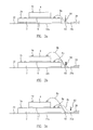
- a planar circuit board 20 is provided (FIGS. 3 a and 4 ).
- the circuit board 20 has a resin layer 22 .
- a chip mounting region 22 a is defined at a center portion of a planar upper surface of the resin layer 22 .
- a plurality of circuit patterns 24 which include bond fingers 24 a , are formed outside the chip mounting region 22 a .
- Conductive transfer patterns 60 are formed on the upper surface of resin layer 22 laterally between the chip mounting region 22 a and the circuit patterns 24 .
- a plurality of semiconductor chips are mounted on the upper surface of circuit board 20 within chip mounting region 22 a.
- a first semiconductor chip 2 is affixed to the upper surface of resin layer 22 within chip mounting region 22 a by an adhesive means 6 , which may be a resin, film, or tape adhesive.
- a smaller second semiconductor chip is affixed using another adhesive means 6 to the upper surface of first semiconductor chip 2 .
- the package may have plural semiconductors arranged adjacent to one another on the upper surface of circuit board 20 , i.e., in the same horizontal plane. Such an MCM package embodiment is discussed further below.
- a lead frame or circuit film can be used in place of circuit board 20 .
- second semiconductor chip 4 is stacked on first semiconductor chip 2 .
- Second semiconductor chip 4 is smaller in area than first semiconductor chip 2 such that second semiconductor chip 4 may be placed between opposing rows of input and output pads 2 a of first semiconductor chip 2 .
- Chips 2 , 4 have input and output pads 2 a , 4 a along all four edges of their upper surfaces (as in FIG. 5 ), or, alternately along only two edges (not shown).
- the input and output pads 2 a of first semiconductor chip 2 of FIG. 5 are in two rows, and the pads 2 a of the two rows are staggered.
- Semiconductor chips 2 , 4 may both be any type of devices, such as memory devices or a combination of two different types of devices, such as a microprocessor and a memory device or a sensor chip and a microprocessor.
- transfer patterns 60 are provided on the upper surface of circuit board 20 beyond the perimeters of semiconductor chips 2 and 4 , as shown in FIGS. 3 a - 3 c , 4 and 5 .
- one end of a first conductive wire 8 a is bonded to an input and output pad 2 a of the first semiconductor chip 2 .
- the other end of the first conductive wire 8 a is then bonded to the transfer pattern 60 (see FIG. 3 a ).
- one end of a second conductive wire 8 b is bonded to an input and output pad 4 a of the second semiconductor chip 4 .
- the other end of the second conductive wire 8 b is then bonded to the same transfer pattern 60 (see FIG. 3 b ).
- the process is repeated for all of the input and output pads of the two semiconductor chips 2 and 4 that are to be electrically interconnected.
- selected input and output pads 2 a of the first semiconductor chip 2 are each electrically connected through a first conductive wire 8 a , transfer pattern 60 , and second conductive wire 8 b to a selected input and output pad 4 a of second semiconductor chip 4 .
- an electrical signal from the first semiconductor chip 2 (or the second semiconductor chip 4 ) may be transferred to the second semiconductor chip 4 (or the first semiconductor chip 2 ) via a first conductive wire 8 a , a transfer pattern 60 , and a second conductive wire 8 b.
- the transfer patterns 60 of the upper surface of circuit board 20 can have a lengthwise direction that is perpendicular or nearly perpendicular to a lengthwise direction of the adjacent circuit patterns 24 that radiate outwardly from the stack of semiconductor chips 2 , 4 and chip mounting region 22 a .
- the transfer patterns 60 can be formed of copper, Alloy 42 , or some other metal and may be plated with silver (Ag) or gold (Au). Other shapes of transfer patterns 60 can be used.
- a predetermined number of circuit patterns 24 among the plurality of circuit patterns 24 can be used as the transfer patterns 60 .
- capillary 50 does not bond the lower end portion of any bond wire to a pre-formed ball 8 d (see FIGS. 2 a - 2 d ), but rather bonds the lower end portions of two separate wires 8 a , 8 b to a planar transfer pattern 60 on the upper surface of circuit board 20 , the forceful vibration energy of capillary 50 or the like is not transmitted to the target semiconductor chip.
- the particular input and output pads and the chip itself are less likely to be broken or cracked relative to the method of FIGS. 2 a - 2 d.
- one end of a third conductive wire 8 c is bonded to selected other input and output pads 2 a (or pads 4 a ) of the first semiconductor chip 2 (of the second semiconductor chip 4 ), and the other end of the third conductive wire 8 c is bonded to one of the bond fingers 24 a of the circuit pattern 24 (see FIG. 3 c ).
- semiconductor chips 2 and 4 may be electrically connected to bond fingers 24 a through wires 8 c , as well as being electrically connected to each other through pairs of wires 8 a , 8 b and an intermediary transfer pattern 60 .
- the second semiconductor chip 4 or the first semiconductor chip 2 may first be electronically connected to the bond fingers 24 a using the third conductive wires 8 c , after which the input and output pads of the first semiconductor chip 2 or the second semiconductor chip 4 may be electronically connected to the transfer pattern(s) 60 using the first or second conductive wires 8 a or 8 b .
- one or more other conductive wires may be connected between a bond finger 24 a and a transfer pattern 60 .
- a voltage may be applied from a circuit pattern 24 to transfer pattern 60 , and from there to chips 2 , 4 .
- FIG. 4 is a cross-sectional side view illustrating a semiconductor package 100 which may be manufactured using the wire bonding method discussed above.
- FIG. 5 is a plan view illustrating an intermediate state of semiconductor package 100 prior to the application an encapsulating material 30 over chips 2 , 4 .
- semiconductor package 100 includes a first semiconductor chip 2 .
- First semiconductor chip 2 has two rows of staggered first input and output pads 2 a on an upper active surface of chip 2 .
- Second semiconductor chip 4 is affixed to the upper surface of the first semiconductor chip 2 by adhesive means 6 .
- Second semiconductor chip 4 has one row of second input and output pads 4 a on an upper surface of semiconductor chip 4 .
- circuit board 20 is affixed to a lower surface of the first semiconductor chip 2 by adhesive means 6 .
- the circuit board 20 includes a core resin layer 22 , which may be a glass-fiber filled organic (e.g., epoxy) laminate.
- Circuit board 20 includes a plurality of conductive circuit patterns 24 outside perimeter of first semiconductor chip 2 (see FIG. 5 ).
- the circuit patterns 24 extend radially from chip 2 toward the perimeter of circuit board 20 .
- the circuit patterns 24 include the bond fingers 24 a .
- Other conductive circuit patterns 24 which include ball lands 24 b , are formed on a lower surface of the resin layer 22 (see FIG. 4 ).
- the circuit patterns 24 are formed of copper (Cu), Alloy 42 , or the like.
- the bond fingers 24 a are plated with silver (Ag) or gold (Ag) so as to improve a connection with the conductive wires subsequently bonded to bond fingers 24 .
- the ball lands 24 b are plated with silver (Ag), nickel (Ni), palladium (Pd), or the like so as to enhance a fused connection to a conductive ball 40 .
- upper surface portions of the circuit patterns 24 excluding the bond fingers 24 a and the ball lands 24 b , are coated with insulative cover coats 26 and the like, so as to be protected from an external environment.
- circuit patterns 24 of the upper and lower surfaces of circuit board 20 are electrically connected with each other through conductive via-holes 25 extending vertically through resin layer 22 .
- Via-holes 25 may be formed of copper plated on the inner walls of a hole through resin layer 22 .
- the one or more transfer patterns 60 are electrically-isolated, planar, rectangular, island-like pads formed on the upper surface of resin layer 22 at predetermined locations between the perimeter of the first semiconductor chip 2 and the bond fingers 24 a .
- Transfer patterns 60 may be formed so as to have a lengthwise direction that is perpendicular to or substantially perpendicular to the lengthwise direction of the circuit patterns 24 .
- transfer patterns 60 are shown, but of course the number of transfer patterns can vary depending, for example, on the number of electrical connections to be made between semiconductor chips 2 and 4 .
- only one transfer pattern 60 may be formed.
- a total of eight transfer patterns 60 may be formed, two adjacent each of the four sides of semiconductor chip 2 . It is not necessary that all of the transfer patterns 60 ultimately are used as bond wire connection points.
- transfer patterns 60 may vary. In the embodiments of FIGS. 3 a — 3 a , 4 , and 5 , transfer patterns 60 are short rectangular strips that are electrically isolated from the laterally adjacent circuit patterns 24 of circuit board 20 . Typically, transfer patterns 60 are formed of the same electrically conductive materials as circuit patterns 24 , and are formed simultaneously with circuit patterns 24 . For example, circuit patterns 24 and transfer patterns 60 may be formed by photolithographic masking and etching of a copper foil that is laminated onto the upper surface of resin layer 22 . The upper surface of transfer patterns 60 may be plated with silver (Ag), gold (Au) or the like so as to ensure easy bonding thereof to the conductive wires 8 a and 8 b . Cover coating 26 (FIG. 4) is not applied over transfer patterns 60 .
- predetermined number of circuit patterns among the plurality of circuit patterns can be used as transfer patterns 60 .
- the input and output pads 2 a of the first semiconductor chip 2 and the transfer patterns 60 are electrically connected to each other by the first conductive wires 8 a .
- the input and output pads 4 a of the second semiconductor chip 4 and the transfer patterns 60 are electrically connected to each other by the second conductive wires 8 b .
- the number of conductive wires 8 a , 8 b connected to each transfer pattern 60 may vary.
- the two transfer pads 60 illustrated in FIG. 5 have two and three bond wire connections, respectively.
- the input and output pads 2 a or 4 a of the first semiconductor chip 2 and/or the second semiconductor chip 4 are electrically connected to the bond fingers 24 a by the third conductive wires 8 c.
- an electrical signal (for example, a ground voltage or a power-supply voltage or a data signal) originating from the first semiconductor chip 2 may be transferred to the transfer pattern 60 via the first conductive wire 8 a , and from there be transferred to the second semiconductor chip 4 via the second conductive wire 8 b that is connected to that transfer pattern 60 .
- an electrical signal originating from the second semiconductor chip 4 may be transferred to the transfer pattern 60 via the second conductive wire 8 b , and from there be transferred to the first semiconductor chip 2 via the first conductive wire 8 a that is connected to that transfer pattern 60 .
- electrical signals from the first or second semiconductor chips 2 and/or 4 may be transferred to the bond fingers 24 a of circuit patterns 24 via the third conductive wires 8 c .
- the electrical signals transferred from chips 2 , 4 to the bond fingers 24 a and the upper circuit patterns 24 may be transferred to the lower circuit patterns 24 through the conductive via-holes 25 , and vice versa.
- the first semiconductor chip 2 , the second semiconductor chip 4 , and the first, second, and third conductive wires 8 a , 8 b and 8 c , respectfully, and the upper surface of the circuit board 20 , including the transfer patterns 60 , bond fingers 24 a and the upper circuit patterns 24 , are encapsulated with the encapsulating material 30 .
- Encapsulating material 30 may be an epoxy molding compound, a liquid phase encapsulant, or the like.
- the conductive balls 40 which may be solder balls, are fused to the ball lands 24 b of the circuit patterns 24 on the lower surface of the circuit board 20 .
- Balls 40 serve as interconnects so that package 100 can be mounted to a mother board.
- the semiconductor package of the exemplary embodiment includes a printed circuit board 20
- the present invention is not so limited.
- a circuit film comprising a thin insulative film layer (e.g., polyimide), circuit patterns and so forth, or a leadframe can be used.
- FIGS. 6 a , 6 b , 6 c and 7 illustrate another exemplary embodiment of the present invention.
- two first semiconductor chips 2 and two second semiconductor chips 4 are laterally adjacent to each other, thereby forming an MCM package.
- the two first semiconductor chips 2 and the two second semiconductor chips 4 are side by side in the same horizontal plane on the upper surface of resin layer 22 of circuit board 20 .
- Exemplary methods of wire bonding and assembling an MCM package along the lines of FIGS. 6 a , 6 b , 6 c and 7 are similar to the methods described above for making stacked semiconductor package 100 .
- a printed circuit board 20 comprising a core resin layer 22 is provided. Electrically conductive circuit patterns 24 are provided on the upper and lower surfaces of resin layer 22 , and are electrically connected through resin layer 22 by via-holes 24 , similar to FIG. 4 .
- a selected number of rectangular, planar, electrically isolated, electrically conductive, island-like pads, called transfer patterns 60 herein, are formed in a cross-pattern on the upper surface of resin layer 22 between adjacent pairs of semiconductor chips 2 , 4 .
- the number, size, and shape of transfer patterns 60 may vary with the application, e.g., according to the number of semiconductor chips 2 , 4 and the number of interconnections to be made between the adjacent semiconductor chips. In this instance, eleven rectangular transfer patterns 60 of varying sizes are provided on the upper surface of resin layer 22 .
- Printed circuit board 20 could be replaced by a circuit film or a leadframe, as mentioned above.
- a selected number of semiconductor chips 2 , 4 are placed in laterally adjacent positions in a central chip mounting region 22 a on the upper surface of resin layer 22 of circuit board 20 , and are attached thereto by an adhesive means 6 , such as a resin, an adhesive film, or a double-sided tape.
- an adhesive means 6 such as a resin, an adhesive film, or a double-sided tape.
- two first semiconductor chips 2 and two second semiconductor chips 4 are mounted side-by-side on the upper surface of circuit board 20 .
- a first conductive wire 8 a is electrically connected between each of a selected number of first bonding pads 2 a and one of the transfer patterns 60 by capillary 50 of a wire bonder.
- a second conductive wire 8 b is electrically connected between each of a selected number of second bond pads 4 a of second semiconductor chip 4 and one of the transfer patterns 60 to which a first conductive wires 8 a was connected.
- first bonding pads 2 a of first semiconductor chip 2 are each electrically connected to s second bonding pad(s) 4 a of second semiconductor chip 4 through a pair of wires 8 a , 8 b and an intermediate transfer pattern 60 , semiconductor chips 2 and 4 are electrically interconnected.
- the order of connection may vary.
- selected bonding pads 2 a , 4 a of semiconductor chips 2 and 4 may each be electrically connected to a bond finger 24 a of circuit patterns 24 by connecting a third conductive wire 8 c therebetween.
- the two first semiconductor chips 2 may be electrically connected through a pair of first conductive wires 8 a that are each electrically connected to a transfer pattern 60
- the two second semiconductor chips 4 may be electrically connected through a pair of second conductive wires 8 b that are each electrically connected to a transfer pattern 60 .
- circuit patterns 24 and transfer patterns 60 may be formed simultaneously from metal foils (e.g., Cu) laminated onto resin layer 22 , and may be plated with silver, or gold, or the like.
- metal foils e.g., Cu
- the MCM shown in FIG. 7 as having four semiconductor chips 2 , 4 is merely exemplary.
- a different number or arrangement of semiconductor chips maybe included in the MCM, along with other components, such as surface mount resistors, capacitors, or inductors.
- the wire bonding method and the semiconductor package manufactured using the method may be obtained in higher yields than is obtainable with the conventional practice described above.
Landscapes
- Wire Bonding (AREA)
Abstract
Description
Claims (22)
Priority Applications (1)
| Application Number | Priority Date | Filing Date | Title |
|---|---|---|---|
| US10/423,702 US6803254B2 (en) | 1999-12-20 | 2003-04-25 | Wire bonding method for a semiconductor package |
Applications Claiming Priority (4)
| Application Number | Priority Date | Filing Date | Title |
|---|---|---|---|
| KR1999-59329 | 1999-12-20 | ||
| KR1019990059329A KR20010064907A (en) | 1999-12-20 | 1999-12-20 | wire bonding method and semiconductor package using it |
| US09/745,265 US6642610B2 (en) | 1999-12-20 | 2000-12-20 | Wire bonding method and semiconductor package manufactured using the same |
| US10/423,702 US6803254B2 (en) | 1999-12-20 | 2003-04-25 | Wire bonding method for a semiconductor package |
Related Parent Applications (1)
| Application Number | Title | Priority Date | Filing Date |
|---|---|---|---|
| US09/745,265 Division US6642610B2 (en) | 1999-12-20 | 2000-12-20 | Wire bonding method and semiconductor package manufactured using the same |
Publications (2)
| Publication Number | Publication Date |
|---|---|
| US20030199118A1 US20030199118A1 (en) | 2003-10-23 |
| US6803254B2 true US6803254B2 (en) | 2004-10-12 |
Family
ID=19627227
Family Applications (2)
| Application Number | Title | Priority Date | Filing Date |
|---|---|---|---|
| US09/745,265 Expired - Lifetime US6642610B2 (en) | 1999-12-20 | 2000-12-20 | Wire bonding method and semiconductor package manufactured using the same |
| US10/423,702 Expired - Lifetime US6803254B2 (en) | 1999-12-20 | 2003-04-25 | Wire bonding method for a semiconductor package |
Family Applications Before (1)
| Application Number | Title | Priority Date | Filing Date |
|---|---|---|---|
| US09/745,265 Expired - Lifetime US6642610B2 (en) | 1999-12-20 | 2000-12-20 | Wire bonding method and semiconductor package manufactured using the same |
Country Status (3)
| Country | Link |
|---|---|
| US (2) | US6642610B2 (en) |
| JP (1) | JP2001189415A (en) |
| KR (1) | KR20010064907A (en) |
Cited By (8)
| Publication number | Priority date | Publication date | Assignee | Title |
|---|---|---|---|---|
| US20040113250A1 (en) * | 2002-12-12 | 2004-06-17 | Khandros Igor Y. | Integrated circuit assembly |
| US20040212096A1 (en) * | 2003-04-23 | 2004-10-28 | Advanced Semiconductor Engineering, Inc. | Multi-chips stacked package |
| US20050184398A1 (en) * | 2004-02-25 | 2005-08-25 | Binling Zhou | Daisy chaining of serial I/O interface on stacking devices |
| US20060049506A1 (en) * | 2004-09-08 | 2006-03-09 | Denso Corporation | Capacitance type semiconductor sensor |
| US20060220200A1 (en) * | 2005-04-01 | 2006-10-05 | Lingsen Precision Industries, Ltd. | Substrate for IC package |
| US20080315432A1 (en) * | 2003-10-01 | 2008-12-25 | Koninklijke Philips Electronics N.V. | Electrical Shielding in Stacked Dies by Using Conductive Die Dttach Adhesive |
| US20090128172A1 (en) * | 2005-08-31 | 2009-05-21 | Advantest Corporation | Calibration board for electronic device test apparatus |
| WO2015006655A1 (en) * | 2013-07-11 | 2015-01-15 | Texas Instruments Incorporated | Semiconductor device having three terminal miniature package |
Families Citing this family (47)
| Publication number | Priority date | Publication date | Assignee | Title |
|---|---|---|---|---|
| US6642136B1 (en) | 2001-09-17 | 2003-11-04 | Megic Corporation | Method of making a low fabrication cost, high performance, high reliability chip scale package |
| US7247932B1 (en) | 2000-05-19 | 2007-07-24 | Megica Corporation | Chip package with capacitor |
| US6815324B2 (en) | 2001-02-15 | 2004-11-09 | Megic Corporation | Reliable metal bumps on top of I/O pads after removal of test probe marks |
| TWI313507B (en) | 2002-10-25 | 2009-08-11 | Megica Corporatio | Method for assembling chips |
| KR100401020B1 (en) * | 2001-03-09 | 2003-10-08 | 앰코 테크놀로지 코리아 주식회사 | Stacking structure of semiconductor chip and semiconductor package using it |
| EP1251577B1 (en) * | 2001-04-19 | 2007-04-25 | Interuniversitair Microelektronica Centrum Vzw | Fabrication of integrated tunable/switchable passive microwave and millimeter wave modules |
| US6680219B2 (en) * | 2001-08-17 | 2004-01-20 | Qualcomm Incorporated | Method and apparatus for die stacking |
| US6613606B1 (en) | 2001-09-17 | 2003-09-02 | Magic Corporation | Structure of high performance combo chip and processing method |
| US7099293B2 (en) | 2002-05-01 | 2006-08-29 | Stmicroelectronics, Inc. | Buffer-less de-skewing for symbol combination in a CDMA demodulator |
| JP3886793B2 (en) * | 2001-12-03 | 2007-02-28 | 株式会社ルネサステクノロジ | Semiconductor integrated circuit device |
| US7021520B2 (en) * | 2001-12-05 | 2006-04-04 | Micron Technology, Inc. | Stacked chip connection using stand off stitch bonding |
| JP3865055B2 (en) * | 2001-12-28 | 2007-01-10 | セイコーエプソン株式会社 | Manufacturing method of semiconductor device |
| TWI237354B (en) * | 2002-01-31 | 2005-08-01 | Advanced Semiconductor Eng | Stacked package structure |
| JP2004028885A (en) * | 2002-06-27 | 2004-01-29 | Fujitsu Ltd | Semiconductor device, semiconductor package, and method of testing semiconductor device |
| DE10251527B4 (en) * | 2002-11-04 | 2007-01-25 | Infineon Technologies Ag | Method for producing a stack arrangement of a memory module |
| JP2004214258A (en) * | 2002-12-27 | 2004-07-29 | Renesas Technology Corp | Semiconductor module |
| KR100555495B1 (en) * | 2003-02-08 | 2006-03-03 | 삼성전자주식회사 | Mold die for chip array molding, molding apparatus comprising the same, and chip array molding method |
| US7185821B1 (en) * | 2003-07-07 | 2007-03-06 | Cisco Technology, Inc. | Method and apparatus for delivering high-current power and ground voltages using top side of chip package substrate |
| US7306971B2 (en) * | 2004-03-02 | 2007-12-11 | Chippac Inc. | Semiconductor chip packaging method with individually placed film adhesive pieces |
| JP2006049569A (en) * | 2004-08-04 | 2006-02-16 | Sharp Corp | Stacked semiconductor device package and manufacturing method thereof |
| US8294279B2 (en) | 2005-01-25 | 2012-10-23 | Megica Corporation | Chip package with dam bar restricting flow of underfill |
| JP4808979B2 (en) * | 2005-03-18 | 2011-11-02 | 株式会社リコー | Multi-chip type semiconductor device and manufacturing method thereof |
| DE102005035393B4 (en) * | 2005-07-28 | 2007-05-24 | Infineon Technologies Ag | A method of manufacturing a multi-chip device and such a device |
| KR100725517B1 (en) * | 2005-08-08 | 2007-06-07 | 삼성전자주식회사 | Multi-layer wiring board having bonding pads and ball lands formed in a plurality of layers and semiconductor package structure using the same |
| JP2007048915A (en) * | 2005-08-09 | 2007-02-22 | Fujitsu Media Device Kk | Semiconductor device |
| SG135074A1 (en) | 2006-02-28 | 2007-09-28 | Micron Technology Inc | Microelectronic devices, stacked microelectronic devices, and methods for manufacturing such devices |
| US7675180B1 (en) | 2006-02-17 | 2010-03-09 | Amkor Technology, Inc. | Stacked electronic component package having film-on-wire spacer |
| US7633144B1 (en) | 2006-05-24 | 2009-12-15 | Amkor Technology, Inc. | Semiconductor package |
| US8861214B1 (en) * | 2006-11-22 | 2014-10-14 | Marvell International Ltd. | High resistivity substrate for integrated passive device (IPD) applications |
| US8110899B2 (en) * | 2006-12-20 | 2012-02-07 | Intel Corporation | Method for incorporating existing silicon die into 3D integrated stack |
| KR100825797B1 (en) * | 2006-12-20 | 2008-04-28 | 삼성전자주식회사 | Semiconductor package and manufacturing method |
| EP2130222B1 (en) * | 2007-02-14 | 2018-09-05 | III Holdings 6, LLC | A carrier for bonding a semiconductor chip onto and a method of contacting a semiconductor chip to a carrier |
| US20080251908A1 (en) * | 2007-04-11 | 2008-10-16 | Advanced Chip Engineering Technology Inc. | Semiconductor device package having multi-chips with side-by-side configuration and method of the same |
| JP4489094B2 (en) * | 2007-04-27 | 2010-06-23 | 株式会社東芝 | Semiconductor package |
| US8836115B1 (en) | 2008-07-31 | 2014-09-16 | Amkor Technology, Inc. | Stacked inverted flip chip package and fabrication method |
| US9009393B1 (en) | 2008-09-23 | 2015-04-14 | Marvell International Ltd. | Hybrid solid-state disk (SSD)/hard disk drive (HDD) architectures |
| US8253231B2 (en) * | 2008-09-23 | 2012-08-28 | Marvell International Ltd. | Stacked integrated circuit package using a window substrate |
| US8896126B2 (en) | 2011-08-23 | 2014-11-25 | Marvell World Trade Ltd. | Packaging DRAM and SOC in an IC package |
| US8387238B2 (en) * | 2009-06-14 | 2013-03-05 | Jayna Sheats | Processes and structures for IC fabrication |
| JP5514134B2 (en) * | 2011-02-14 | 2014-06-04 | ルネサスエレクトロニクス株式会社 | Manufacturing method of semiconductor device |
| JP2014027145A (en) * | 2012-07-27 | 2014-02-06 | Toshiba Corp | Semiconductor device |
| TWI522012B (en) * | 2013-11-19 | 2016-02-11 | 碩頡科技股份有限公司 | Integrated light source driving circuit and light source module using the same |
| KR102499954B1 (en) * | 2016-10-24 | 2023-02-15 | 삼성전자주식회사 | Multi-chip package and method of manufacturing the same |
| US10600756B1 (en) | 2017-02-15 | 2020-03-24 | United States Of America, As Represented By The Secretary Of The Navy | Wire bonding technique for integrated circuit board connections |
| CN108878408A (en) * | 2017-05-10 | 2018-11-23 | 叶秀慧 | It is thinned the encapsulating structure that splices of dual chip |
| KR102582066B1 (en) * | 2018-04-17 | 2023-09-25 | 삼성디스플레이 주식회사 | Chip on film package and display device including the chip on film package |
| CN115485820A (en) | 2021-03-11 | 2022-12-16 | 日东电工株式会社 | Method for producing cured resin sheet with electrode, and thermosetting resin sheet |
Citations (91)
| Publication number | Priority date | Publication date | Assignee | Title |
|---|---|---|---|---|
| US3851221A (en) | 1972-11-30 | 1974-11-26 | P Beaulieu | Integrated circuit package |
| JPS54128274A (en) | 1978-03-29 | 1979-10-04 | Hitachi Ltd | Resin-sealed semiconductor device |
| JPS5662351A (en) | 1979-10-26 | 1981-05-28 | Hitachi Ltd | Semiconductor device for memory |
| JPS60182731A (en) | 1984-02-29 | 1985-09-18 | Toshiba Corp | Semiconductor device |
| US4567643A (en) | 1983-10-24 | 1986-02-04 | Sintra-Alcatel | Method of replacing an electronic component connected to conducting tracks on a support substrate |
| JPS6159862A (en) | 1984-08-31 | 1986-03-27 | Fujitsu Ltd | Semiconductor device |
| JPS61117858A (en) | 1984-11-14 | 1986-06-05 | Hitachi Micro Comput Eng Ltd | Semiconductor device |
| JPS62119952A (en) | 1985-11-19 | 1987-06-01 | Nec Corp | Integrated circuit device |
| JPS62126661A (en) | 1985-11-27 | 1987-06-08 | Nec Corp | Hybrid integrated circuit device |
| JPS62142341A (en) | 1985-12-17 | 1987-06-25 | Matsushita Electronics Corp | Semiconductor device and manufacture thereof |
| US4730232A (en) | 1986-06-25 | 1988-03-08 | Westinghouse Electric Corp. | High density microelectronic packaging module for high speed chips |
| JPS63128736A (en) | 1986-11-19 | 1988-06-01 | Olympus Optical Co Ltd | Semiconductor element |
| US4763188A (en) | 1986-08-08 | 1988-08-09 | Thomas Johnson | Packaging system for multiple semiconductor devices |
| JPS63211663A (en) | 1987-02-26 | 1988-09-02 | Mitsubishi Electric Corp | Circuit board |
| JPS63244654A (en) | 1987-03-31 | 1988-10-12 | Toshiba Corp | Plastic molded type integrated circuit device |
| JPS641269A (en) | 1987-06-24 | 1989-01-05 | Hitachi Ltd | Semiconductor device |
| JPS6428856A (en) | 1987-07-23 | 1989-01-31 | Mitsubishi Electric Corp | Multilayered integrated circuit |
| JPS6471162A (en) | 1987-09-11 | 1989-03-16 | Hitachi Ltd | Semiconductor device |
| JPH0199248A (en) | 1987-10-13 | 1989-04-18 | Mitsubishi Electric Corp | Semiconductor device |
| US4982265A (en) | 1987-06-24 | 1991-01-01 | Hitachi, Ltd. | Semiconductor integrated circuit device and method of manufacturing the same |
| US4996587A (en) | 1989-04-10 | 1991-02-26 | International Business Machines Corporation | Integrated semiconductor chip package |
| US5012323A (en) | 1989-11-20 | 1991-04-30 | Micron Technology, Inc. | Double-die semiconductor package having a back-bonded die and a face-bonded die interconnected on a single leadframe |
| US5025306A (en) | 1988-08-09 | 1991-06-18 | Texas Instruments Incorporated | Assembly of semiconductor chips |
| JPH03169062A (en) | 1989-11-28 | 1991-07-22 | Nec Kyushu Ltd | Semiconductor device |
| US5040052A (en) | 1987-12-28 | 1991-08-13 | Texas Instruments Incorporated | Compact silicon module for high density integrated circuits |
| JPH0428260A (en) | 1990-05-23 | 1992-01-30 | Matsushita Electric Ind Co Ltd | Method of mounting semiconductor chip |
| JPH0456262A (en) | 1990-06-25 | 1992-02-24 | Matsushita Electron Corp | Semiconductor integrated circuit device |
| JPH0496358A (en) | 1990-08-13 | 1992-03-27 | Casio Comput Co Ltd | Printed wiring board |
| JPH04116859A (en) | 1990-09-06 | 1992-04-17 | Mitsubishi Electric Corp | Semiconductor device |
| US5124783A (en) | 1989-01-30 | 1992-06-23 | Kabushiki Kaisha Toshiba | Semiconductor device having insulating substrate adhered to conductive substrate |
| US5138438A (en) | 1987-06-24 | 1992-08-11 | Akita Electronics Co. Ltd. | Lead connections means for stacked tab packaged IC chips |
| US5140404A (en) | 1990-10-24 | 1992-08-18 | Micron Technology, Inc. | Semiconductor device manufactured by a method for attaching a semiconductor die to a leadframe using a thermoplastic covered carrier tape |
| EP0503201A2 (en) | 1990-12-20 | 1992-09-16 | Kabushiki Kaisha Toshiba | Semiconductor device having an interconnecting circuit board and method for manufacturing same |
| US5165067A (en) | 1989-12-01 | 1992-11-17 | Inmos Limited | Semiconductor chip packages |
| US5168368A (en) | 1991-05-09 | 1992-12-01 | International Business Machines Corporation | Lead frame-chip package with improved configuration |
| JPH04368167A (en) | 1991-06-14 | 1992-12-21 | Yamaha Corp | Electronic device |
| JPH04368154A (en) | 1991-06-15 | 1992-12-21 | Sony Corp | Semiconductor device |
| JPH0513665A (en) | 1991-06-28 | 1993-01-22 | Nec Corp | TAB chip mounting method |
| JPH0575015A (en) | 1991-09-13 | 1993-03-26 | Sharp Corp | Semiconductor device |
| US5198888A (en) | 1987-12-28 | 1993-03-30 | Hitachi, Ltd. | Semiconductor stacked device |
| JPH05109975A (en) | 1991-10-14 | 1993-04-30 | Hitachi Ltd | Resin-sealed type semiconductor device |
| JPH05136323A (en) | 1991-11-13 | 1993-06-01 | Nec Corp | Integrated circuit device |
| US5229647A (en) | 1991-03-27 | 1993-07-20 | Micron Technology, Inc. | High density data storage using stacked wafers |
| US5273938A (en) | 1989-09-06 | 1993-12-28 | Motorola, Inc. | Method for attaching conductive traces to plural, stacked, encapsulated semiconductor die using a removable transfer film |
| US5291061A (en) | 1993-04-06 | 1994-03-01 | Micron Semiconductor, Inc. | Multi-chip stacked devices |
| US5323060A (en) | 1993-06-02 | 1994-06-21 | Micron Semiconductor, Inc. | Multichip module having a stacked chip arrangement |
| US5334875A (en) | 1987-12-28 | 1994-08-02 | Hitachi, Ltd. | Stacked semiconductor memory device and semiconductor memory module containing the same |
| US5347429A (en) | 1990-11-14 | 1994-09-13 | Hitachi, Ltd. | Plastic-molded-type semiconductor device |
| US5422435A (en) | 1992-05-22 | 1995-06-06 | National Semiconductor Corporation | Stacked multi-chip modules and method of manufacturing |
| US5426563A (en) | 1992-08-05 | 1995-06-20 | Fujitsu Limited | Three-dimensional multichip module |
| US5432729A (en) | 1993-04-23 | 1995-07-11 | Irvine Sensors Corporation | Electronic module comprising a stack of IC chips each interacting with an IC chip secured to the stack |
| US5462624A (en) | 1992-12-22 | 1995-10-31 | Vlsi Technology, Inc. | Embedded inter-connect frame |
| US5463253A (en) | 1990-03-15 | 1995-10-31 | Fujitsu Limited | Semiconductor device having a plurality of chips |
| US5473196A (en) | 1993-02-02 | 1995-12-05 | Matra Marconi Space France | Semiconductor memory component comprising stacked memory modules |
| US5495394A (en) | 1994-12-19 | 1996-02-27 | At&T Global Information Solutions Company | Three dimensional die packaging in multi-chip modules |
| US5498901A (en) | 1994-08-23 | 1996-03-12 | National Semiconductor Corporation | Lead frame having layered conductive planes |
| US5514907A (en) | 1995-03-21 | 1996-05-07 | Simple Technology Incorporated | Apparatus for stacking semiconductor chips |
| US5569625A (en) | 1992-01-08 | 1996-10-29 | Fujitsu Limited | Process for manufacturing a plural stacked leadframe semiconductor device |
| US5581498A (en) | 1993-08-13 | 1996-12-03 | Irvine Sensors Corporation | Stack of IC chips in lieu of single IC chip |
| US5614766A (en) | 1991-09-30 | 1997-03-25 | Rohm Co., Ltd. | Semiconductor device with stacked alternate-facing chips |
| US5637536A (en) | 1993-08-13 | 1997-06-10 | Thomson-Csf | Method for interconnecting semiconductor chips in three dimensions, and component resulting therefrom |
| US5637912A (en) | 1994-08-22 | 1997-06-10 | International Business Machines Corporation | Three-dimensional monolithic electronic module having stacked planar arrays of integrated circuit chips |
| US5682062A (en) | 1995-06-05 | 1997-10-28 | Harris Corporation | System for interconnecting stacked integrated circuits |
| US5689135A (en) | 1995-12-19 | 1997-11-18 | Micron Technology, Inc. | Multi-chip device and method of fabrication employing leads over and under processes |
| US5696031A (en) | 1996-11-20 | 1997-12-09 | Micron Technology, Inc. | Device and method for stacking wire-bonded integrated circuit dice on flip-chip bonded integrated circuit dice |
| US5721452A (en) | 1995-08-16 | 1998-02-24 | Micron Technology, Inc. | Angularly offset stacked die multichip device and method of manufacture |
| US5739581A (en) | 1995-11-17 | 1998-04-14 | National Semiconductor Corporation | High density integrated circuit package assembly with a heatsink between stacked dies |
| US5783870A (en) | 1995-03-16 | 1998-07-21 | National Semiconductor Corporation | Method for connecting packages of a stacked ball grid array structure |
| US5793108A (en) | 1995-05-30 | 1998-08-11 | Sharp Kabushiki Kaisha | Semiconductor integrated circuit having a plurality of semiconductor chips |
| US5798014A (en) | 1995-02-02 | 1998-08-25 | Hestia Technologies, Inc. | Methods of making multi-tier laminate substrates for electronic device packaging |
| JPH10256470A (en) | 1997-03-10 | 1998-09-25 | Sanyo Electric Co Ltd | Semiconductor device |
| US5815372A (en) | 1997-03-25 | 1998-09-29 | Intel Corporation | Packaging multiple dies on a ball grid array substrate |
| US5861666A (en) | 1995-08-30 | 1999-01-19 | Tessera, Inc. | Stacked chip assembly |
| US5872025A (en) | 1995-07-26 | 1999-02-16 | International Business Machines Corporation | Method for stacked three dimensional device manufacture |
| US5885849A (en) | 1995-03-28 | 1999-03-23 | Tessera, Inc. | Methods of making microelectronic assemblies |
| US5886412A (en) | 1995-08-16 | 1999-03-23 | Micron Technology, Inc. | Angularly offset and recessed stacked die multichip device |
| US5917242A (en) | 1996-05-20 | 1999-06-29 | Micron Technology, Inc. | Combination of semiconductor interconnect |
| US5952611A (en) | 1997-12-19 | 1999-09-14 | Texas Instruments Incorporated | Flexible pin location integrated circuit package |
| US6005778A (en) | 1995-06-15 | 1999-12-21 | Honeywell Inc. | Chip stacking and capacitor mounting arrangement including spacers |
| US6051886A (en) | 1995-08-16 | 2000-04-18 | Micron Technology, Inc. | Angularly offset stacked die multichip device and method of manufacture |
| US6057598A (en) | 1997-01-31 | 2000-05-02 | Vlsi Technology, Inc. | Face on face flip chip integration |
| US6072243A (en) | 1996-11-26 | 2000-06-06 | Sharp Kabushiki Kaisha | Semiconductor integrated circuit device capable of surely electrically insulating two semiconductor chips from each other and fabricating method thereof |
| US6133637A (en) | 1997-01-24 | 2000-10-17 | Rohm Co., Ltd. | Semiconductor device having a plurality of semiconductor chips |
| US6161753A (en) * | 1999-11-01 | 2000-12-19 | Advanced Semiconductor Engineering, Inc. | Method of making a low-profile wire connection for stacked dies |
| US6184463B1 (en) | 1998-04-13 | 2001-02-06 | Harris Corporation | Integrated circuit package for flip chip |
| US6214641B1 (en) | 1996-06-25 | 2001-04-10 | Micron Technology, Inc. | Method of fabricating a multi-chip module |
| US6232561B1 (en) | 1997-01-31 | 2001-05-15 | Robert Bosch Gmbh | Process for producing wire connections on an electronic component assembly carrier made by the process |
| JP3169062B2 (en) | 1996-07-11 | 2001-05-21 | 日産化学工業株式会社 | Liquid crystal cell alignment agent |
| US6235554B1 (en) | 1995-11-27 | 2001-05-22 | Micron Technology, Inc. | Method for fabricating stackable chip scale semiconductor package |
| US6316838B1 (en) | 1999-10-29 | 2001-11-13 | Fujitsu Limited | Semiconductor device |
| US6340842B1 (en) | 1998-04-02 | 2002-01-22 | Oki Electric Industry Co., Ltd. | Semiconductor device in a recess of a semiconductor plate |
Family Cites Families (7)
| Publication number | Priority date | Publication date | Assignee | Title |
|---|---|---|---|---|
| JPH01235363A (en) * | 1988-03-16 | 1989-09-20 | Hitachi Ltd | Semiconductor device |
| JPH0513663A (en) * | 1991-07-09 | 1993-01-22 | Fujitsu Ltd | Semiconductor device and mounting method of semiconductor chip |
| JPH11135537A (en) * | 1997-10-29 | 1999-05-21 | Rohm Co Ltd | Semiconductor chip mounting structure and semiconductor device |
| JPH11121496A (en) * | 1997-10-14 | 1999-04-30 | Rohm Co Ltd | Semiconductor chip mounting structure and semiconductor device |
| JP3481444B2 (en) * | 1998-01-14 | 2003-12-22 | シャープ株式会社 | Semiconductor device and manufacturing method thereof |
| JPH11310150A (en) * | 1998-04-28 | 1999-11-09 | Daihatsu Motor Co Ltd | Mounting structure for sub-frame |
| KR20000061035A (en) * | 1999-03-23 | 2000-10-16 | 최완균 | Semiconductor chip, method for manufacturing the semiconductor chip, stacked chip package using the semiconductor chip and method for manufacturing the stacked chip package |
-
1999
- 1999-12-20 KR KR1019990059329A patent/KR20010064907A/en not_active Ceased
-
2000
- 2000-10-10 JP JP2000309733A patent/JP2001189415A/en active Pending
- 2000-12-20 US US09/745,265 patent/US6642610B2/en not_active Expired - Lifetime
-
2003
- 2003-04-25 US US10/423,702 patent/US6803254B2/en not_active Expired - Lifetime
Patent Citations (100)
| Publication number | Priority date | Publication date | Assignee | Title |
|---|---|---|---|---|
| US3851221A (en) | 1972-11-30 | 1974-11-26 | P Beaulieu | Integrated circuit package |
| JPS54128274A (en) | 1978-03-29 | 1979-10-04 | Hitachi Ltd | Resin-sealed semiconductor device |
| JPS5662351A (en) | 1979-10-26 | 1981-05-28 | Hitachi Ltd | Semiconductor device for memory |
| US4567643A (en) | 1983-10-24 | 1986-02-04 | Sintra-Alcatel | Method of replacing an electronic component connected to conducting tracks on a support substrate |
| JPS60182731A (en) | 1984-02-29 | 1985-09-18 | Toshiba Corp | Semiconductor device |
| JPS6159862A (en) | 1984-08-31 | 1986-03-27 | Fujitsu Ltd | Semiconductor device |
| JPS61117858A (en) | 1984-11-14 | 1986-06-05 | Hitachi Micro Comput Eng Ltd | Semiconductor device |
| JPS62119952A (en) | 1985-11-19 | 1987-06-01 | Nec Corp | Integrated circuit device |
| JPS62126661A (en) | 1985-11-27 | 1987-06-08 | Nec Corp | Hybrid integrated circuit device |
| JPS62142341A (en) | 1985-12-17 | 1987-06-25 | Matsushita Electronics Corp | Semiconductor device and manufacture thereof |
| US4730232A (en) | 1986-06-25 | 1988-03-08 | Westinghouse Electric Corp. | High density microelectronic packaging module for high speed chips |
| US4763188A (en) | 1986-08-08 | 1988-08-09 | Thomas Johnson | Packaging system for multiple semiconductor devices |
| JPS63128736A (en) | 1986-11-19 | 1988-06-01 | Olympus Optical Co Ltd | Semiconductor element |
| JPS63211663A (en) | 1987-02-26 | 1988-09-02 | Mitsubishi Electric Corp | Circuit board |
| JPS63244654A (en) | 1987-03-31 | 1988-10-12 | Toshiba Corp | Plastic molded type integrated circuit device |
| US4982265A (en) | 1987-06-24 | 1991-01-01 | Hitachi, Ltd. | Semiconductor integrated circuit device and method of manufacturing the same |
| US5587341A (en) | 1987-06-24 | 1996-12-24 | Hitachi, Ltd. | Process for manufacturing a stacked integrated circuit package |
| US5138438A (en) | 1987-06-24 | 1992-08-11 | Akita Electronics Co. Ltd. | Lead connections means for stacked tab packaged IC chips |
| JPS641269A (en) | 1987-06-24 | 1989-01-05 | Hitachi Ltd | Semiconductor device |
| JPS6428856A (en) | 1987-07-23 | 1989-01-31 | Mitsubishi Electric Corp | Multilayered integrated circuit |
| JPS6471162A (en) | 1987-09-11 | 1989-03-16 | Hitachi Ltd | Semiconductor device |
| JPH0199248A (en) | 1987-10-13 | 1989-04-18 | Mitsubishi Electric Corp | Semiconductor device |
| US5040052A (en) | 1987-12-28 | 1991-08-13 | Texas Instruments Incorporated | Compact silicon module for high density integrated circuits |
| US5198888A (en) | 1987-12-28 | 1993-03-30 | Hitachi, Ltd. | Semiconductor stacked device |
| US5334875A (en) | 1987-12-28 | 1994-08-02 | Hitachi, Ltd. | Stacked semiconductor memory device and semiconductor memory module containing the same |
| US5025306A (en) | 1988-08-09 | 1991-06-18 | Texas Instruments Incorporated | Assembly of semiconductor chips |
| US5124783A (en) | 1989-01-30 | 1992-06-23 | Kabushiki Kaisha Toshiba | Semiconductor device having insulating substrate adhered to conductive substrate |
| US4996587A (en) | 1989-04-10 | 1991-02-26 | International Business Machines Corporation | Integrated semiconductor chip package |
| US5273938A (en) | 1989-09-06 | 1993-12-28 | Motorola, Inc. | Method for attaching conductive traces to plural, stacked, encapsulated semiconductor die using a removable transfer film |
| US5012323A (en) | 1989-11-20 | 1991-04-30 | Micron Technology, Inc. | Double-die semiconductor package having a back-bonded die and a face-bonded die interconnected on a single leadframe |
| JPH03169062A (en) | 1989-11-28 | 1991-07-22 | Nec Kyushu Ltd | Semiconductor device |
| US5165067A (en) | 1989-12-01 | 1992-11-17 | Inmos Limited | Semiconductor chip packages |
| US5463253A (en) | 1990-03-15 | 1995-10-31 | Fujitsu Limited | Semiconductor device having a plurality of chips |
| JPH0428260A (en) | 1990-05-23 | 1992-01-30 | Matsushita Electric Ind Co Ltd | Method of mounting semiconductor chip |
| JPH0456262A (en) | 1990-06-25 | 1992-02-24 | Matsushita Electron Corp | Semiconductor integrated circuit device |
| JPH0496358A (en) | 1990-08-13 | 1992-03-27 | Casio Comput Co Ltd | Printed wiring board |
| JPH04116859A (en) | 1990-09-06 | 1992-04-17 | Mitsubishi Electric Corp | Semiconductor device |
| US5140404A (en) | 1990-10-24 | 1992-08-18 | Micron Technology, Inc. | Semiconductor device manufactured by a method for attaching a semiconductor die to a leadframe using a thermoplastic covered carrier tape |
| US5347429A (en) | 1990-11-14 | 1994-09-13 | Hitachi, Ltd. | Plastic-molded-type semiconductor device |
| US5715147A (en) | 1990-12-20 | 1998-02-03 | Kabushiki Kaisha Toshiba | Semiconductor device having an interconnecting circuit board |
| JPH05283601A (en) | 1990-12-20 | 1993-10-29 | Toshiba Corp | Semiconductor device having interconnection circuit board and manufacturing method thereof |
| EP0503201A2 (en) | 1990-12-20 | 1992-09-16 | Kabushiki Kaisha Toshiba | Semiconductor device having an interconnecting circuit board and method for manufacturing same |
| US5229647A (en) | 1991-03-27 | 1993-07-20 | Micron Technology, Inc. | High density data storage using stacked wafers |
| US5168368A (en) | 1991-05-09 | 1992-12-01 | International Business Machines Corporation | Lead frame-chip package with improved configuration |
| JPH04368167A (en) | 1991-06-14 | 1992-12-21 | Yamaha Corp | Electronic device |
| JPH04368154A (en) | 1991-06-15 | 1992-12-21 | Sony Corp | Semiconductor device |
| JPH0513665A (en) | 1991-06-28 | 1993-01-22 | Nec Corp | TAB chip mounting method |
| JPH0575015A (en) | 1991-09-13 | 1993-03-26 | Sharp Corp | Semiconductor device |
| US5614766A (en) | 1991-09-30 | 1997-03-25 | Rohm Co., Ltd. | Semiconductor device with stacked alternate-facing chips |
| JPH05109975A (en) | 1991-10-14 | 1993-04-30 | Hitachi Ltd | Resin-sealed type semiconductor device |
| JPH05136323A (en) | 1991-11-13 | 1993-06-01 | Nec Corp | Integrated circuit device |
| US5569625A (en) | 1992-01-08 | 1996-10-29 | Fujitsu Limited | Process for manufacturing a plural stacked leadframe semiconductor device |
| US5422435A (en) | 1992-05-22 | 1995-06-06 | National Semiconductor Corporation | Stacked multi-chip modules and method of manufacturing |
| US5495398A (en) | 1992-05-22 | 1996-02-27 | National Semiconductor Corporation | Stacked multi-chip modules and method of manufacturing |
| US5502289A (en) | 1992-05-22 | 1996-03-26 | National Semiconductor Corporation | Stacked multi-chip modules and method of manufacturing |
| US5426563A (en) | 1992-08-05 | 1995-06-20 | Fujitsu Limited | Three-dimensional multichip module |
| US5462624A (en) | 1992-12-22 | 1995-10-31 | Vlsi Technology, Inc. | Embedded inter-connect frame |
| US5473196A (en) | 1993-02-02 | 1995-12-05 | Matra Marconi Space France | Semiconductor memory component comprising stacked memory modules |
| USRE36613E (en) | 1993-04-06 | 2000-03-14 | Micron Technology, Inc. | Multi-chip stacked devices |
| US5291061A (en) | 1993-04-06 | 1994-03-01 | Micron Semiconductor, Inc. | Multi-chip stacked devices |
| US5432729A (en) | 1993-04-23 | 1995-07-11 | Irvine Sensors Corporation | Electronic module comprising a stack of IC chips each interacting with an IC chip secured to the stack |
| US5323060A (en) | 1993-06-02 | 1994-06-21 | Micron Semiconductor, Inc. | Multichip module having a stacked chip arrangement |
| US5581498A (en) | 1993-08-13 | 1996-12-03 | Irvine Sensors Corporation | Stack of IC chips in lieu of single IC chip |
| US5637536A (en) | 1993-08-13 | 1997-06-10 | Thomson-Csf | Method for interconnecting semiconductor chips in three dimensions, and component resulting therefrom |
| US5637912A (en) | 1994-08-22 | 1997-06-10 | International Business Machines Corporation | Three-dimensional monolithic electronic module having stacked planar arrays of integrated circuit chips |
| US5498901A (en) | 1994-08-23 | 1996-03-12 | National Semiconductor Corporation | Lead frame having layered conductive planes |
| US5495394A (en) | 1994-12-19 | 1996-02-27 | At&T Global Information Solutions Company | Three dimensional die packaging in multi-chip modules |
| US5798014A (en) | 1995-02-02 | 1998-08-25 | Hestia Technologies, Inc. | Methods of making multi-tier laminate substrates for electronic device packaging |
| US5783870A (en) | 1995-03-16 | 1998-07-21 | National Semiconductor Corporation | Method for connecting packages of a stacked ball grid array structure |
| US5514907A (en) | 1995-03-21 | 1996-05-07 | Simple Technology Incorporated | Apparatus for stacking semiconductor chips |
| US5885849A (en) | 1995-03-28 | 1999-03-23 | Tessera, Inc. | Methods of making microelectronic assemblies |
| US5793108A (en) | 1995-05-30 | 1998-08-11 | Sharp Kabushiki Kaisha | Semiconductor integrated circuit having a plurality of semiconductor chips |
| US5682062A (en) | 1995-06-05 | 1997-10-28 | Harris Corporation | System for interconnecting stacked integrated circuits |
| US6005778A (en) | 1995-06-15 | 1999-12-21 | Honeywell Inc. | Chip stacking and capacitor mounting arrangement including spacers |
| US5872025A (en) | 1995-07-26 | 1999-02-16 | International Business Machines Corporation | Method for stacked three dimensional device manufacture |
| US5721452A (en) | 1995-08-16 | 1998-02-24 | Micron Technology, Inc. | Angularly offset stacked die multichip device and method of manufacture |
| US5963794A (en) * | 1995-08-16 | 1999-10-05 | Micron Technology, Inc. | Angularly offset stacked die multichip device and method of manufacture |
| US6051886A (en) | 1995-08-16 | 2000-04-18 | Micron Technology, Inc. | Angularly offset stacked die multichip device and method of manufacture |
| US5886412A (en) | 1995-08-16 | 1999-03-23 | Micron Technology, Inc. | Angularly offset and recessed stacked die multichip device |
| US5861666A (en) | 1995-08-30 | 1999-01-19 | Tessera, Inc. | Stacked chip assembly |
| US5739581A (en) | 1995-11-17 | 1998-04-14 | National Semiconductor Corporation | High density integrated circuit package assembly with a heatsink between stacked dies |
| US6235554B1 (en) | 1995-11-27 | 2001-05-22 | Micron Technology, Inc. | Method for fabricating stackable chip scale semiconductor package |
| US5689135A (en) | 1995-12-19 | 1997-11-18 | Micron Technology, Inc. | Multi-chip device and method of fabrication employing leads over and under processes |
| US5917242A (en) | 1996-05-20 | 1999-06-29 | Micron Technology, Inc. | Combination of semiconductor interconnect |
| US6080264A (en) | 1996-05-20 | 2000-06-27 | Micron Technology, Inc. | Combination of semiconductor interconnect |
| US6214641B1 (en) | 1996-06-25 | 2001-04-10 | Micron Technology, Inc. | Method of fabricating a multi-chip module |
| JP3169062B2 (en) | 1996-07-11 | 2001-05-21 | 日産化学工業株式会社 | Liquid crystal cell alignment agent |
| US5973403A (en) | 1996-11-20 | 1999-10-26 | Micron Technology, Inc. | Device and method for stacking wire-bonded integrated circuit dice on flip-chip bonded integrated circuit dice |
| US5696031A (en) | 1996-11-20 | 1997-12-09 | Micron Technology, Inc. | Device and method for stacking wire-bonded integrated circuit dice on flip-chip bonded integrated circuit dice |
| US6072243A (en) | 1996-11-26 | 2000-06-06 | Sharp Kabushiki Kaisha | Semiconductor integrated circuit device capable of surely electrically insulating two semiconductor chips from each other and fabricating method thereof |
| US6133637A (en) | 1997-01-24 | 2000-10-17 | Rohm Co., Ltd. | Semiconductor device having a plurality of semiconductor chips |
| US6232561B1 (en) | 1997-01-31 | 2001-05-15 | Robert Bosch Gmbh | Process for producing wire connections on an electronic component assembly carrier made by the process |
| US6057598A (en) | 1997-01-31 | 2000-05-02 | Vlsi Technology, Inc. | Face on face flip chip integration |
| JPH10256470A (en) | 1997-03-10 | 1998-09-25 | Sanyo Electric Co Ltd | Semiconductor device |
| US5815372A (en) | 1997-03-25 | 1998-09-29 | Intel Corporation | Packaging multiple dies on a ball grid array substrate |
| US5952611A (en) | 1997-12-19 | 1999-09-14 | Texas Instruments Incorporated | Flexible pin location integrated circuit package |
| US6340842B1 (en) | 1998-04-02 | 2002-01-22 | Oki Electric Industry Co., Ltd. | Semiconductor device in a recess of a semiconductor plate |
| US6184463B1 (en) | 1998-04-13 | 2001-02-06 | Harris Corporation | Integrated circuit package for flip chip |
| US6316838B1 (en) | 1999-10-29 | 2001-11-13 | Fujitsu Limited | Semiconductor device |
| US6161753A (en) * | 1999-11-01 | 2000-12-19 | Advanced Semiconductor Engineering, Inc. | Method of making a low-profile wire connection for stacked dies |
Cited By (14)
| Publication number | Priority date | Publication date | Assignee | Title |
|---|---|---|---|---|
| US20040113250A1 (en) * | 2002-12-12 | 2004-06-17 | Khandros Igor Y. | Integrated circuit assembly |
| US7550842B2 (en) * | 2002-12-12 | 2009-06-23 | Formfactor, Inc. | Integrated circuit assembly |
| US20040212096A1 (en) * | 2003-04-23 | 2004-10-28 | Advanced Semiconductor Engineering, Inc. | Multi-chips stacked package |
| US7268418B2 (en) * | 2003-04-23 | 2007-09-11 | Advanced Semiconductor Engineering, Inc. | Multi-chips stacked package |
| US8076763B2 (en) * | 2003-10-01 | 2011-12-13 | Nxp B.V. | Electrical shielding in stacked dies by using conductive die attach adhesive |
| US20080315432A1 (en) * | 2003-10-01 | 2008-12-25 | Koninklijke Philips Electronics N.V. | Electrical Shielding in Stacked Dies by Using Conductive Die Dttach Adhesive |
| US7173340B2 (en) * | 2004-02-25 | 2007-02-06 | Texas Instruments Incorporated | Daisy chaining of serial I/O interface on stacking devices |
| US20050184398A1 (en) * | 2004-02-25 | 2005-08-25 | Binling Zhou | Daisy chaining of serial I/O interface on stacking devices |
| US7339265B2 (en) * | 2004-09-08 | 2008-03-04 | Denso Corporation | Capacitance type semiconductor sensor |
| US20060049506A1 (en) * | 2004-09-08 | 2006-03-09 | Denso Corporation | Capacitance type semiconductor sensor |
| US7154169B2 (en) * | 2005-04-01 | 2006-12-26 | Lingsen Precision Industries, Ltd. | Substrate for IC package |
| US20060220200A1 (en) * | 2005-04-01 | 2006-10-05 | Lingsen Precision Industries, Ltd. | Substrate for IC package |
| US20090128172A1 (en) * | 2005-08-31 | 2009-05-21 | Advantest Corporation | Calibration board for electronic device test apparatus |
| WO2015006655A1 (en) * | 2013-07-11 | 2015-01-15 | Texas Instruments Incorporated | Semiconductor device having three terminal miniature package |
Also Published As
| Publication number | Publication date |
|---|---|
| US20030199118A1 (en) | 2003-10-23 |
| US6642610B2 (en) | 2003-11-04 |
| JP2001189415A (en) | 2001-07-10 |
| US20020064905A1 (en) | 2002-05-30 |
| KR20010064907A (en) | 2001-07-11 |
Similar Documents
| Publication | Publication Date | Title |
|---|---|---|
| US6803254B2 (en) | Wire bonding method for a semiconductor package | |
| US6876553B2 (en) | Enhanced die-up ball grid array package with two substrates | |
| US8076770B2 (en) | Semiconductor device including a first land on the wiring substrate and a second land on the sealing portion | |
| KR100260997B1 (en) | Semiconductor package | |
| JP3481444B2 (en) | Semiconductor device and manufacturing method thereof | |
| US6781242B1 (en) | Thin ball grid array package | |
| US6300685B1 (en) | Semiconductor package | |
| US6873040B2 (en) | Semiconductor packages for enhanced number of terminals, speed and power performance | |
| JP2001015679A (en) | Semiconductor device and manufacturing method thereof | |
| CN114823651A (en) | Radio frequency system module packaging structure with filter and method | |
| US20220246542A1 (en) | Semiconductor device and method of manufacturing semiconductor device | |
| KR19990006158A (en) | Ball grid array package | |
| US20080157302A1 (en) | Stacked-package quad flat null lead package | |
| US7265441B2 (en) | Stackable single package and stacked multi-chip assembly | |
| KR20010063236A (en) | Stack package and manufacturing method thereof | |
| JP3450477B2 (en) | Semiconductor device and manufacturing method thereof | |
| KR100437821B1 (en) | semiconductor package and metod for fabricating the same | |
| KR19990056764A (en) | Ball grid array package | |
| KR100218633B1 (en) | Ball Grid Array Semiconductor Package with Carrier Frame | |
| KR100247641B1 (en) | Stacked ball grid array package and its manufacturing method | |
| KR19990051002A (en) | Laminated package and its manufacturing method | |
| KR100542672B1 (en) | Semiconductor Package | |
| KR100279249B1 (en) | Stacked Package and Manufacturing Method | |
| KR19990002732U (en) | Ball grid array package | |
| KR20000028360A (en) | Semiconductor device |
Legal Events
| Date | Code | Title | Description |
|---|---|---|---|
| STCF | Information on status: patent grant |
Free format text: PATENTED CASE |
|
| AS | Assignment |
Owner name: BANK OF AMERICA, N.A., TEXAS Free format text: SECURITY AGREEMENT;ASSIGNOR:AMKOR TECHNOLOGY, INC.;REEL/FRAME:017379/0630 Effective date: 20051123 |
|
| FPAY | Fee payment |
Year of fee payment: 4 |
|
| REMI | Maintenance fee reminder mailed | ||
| FPAY | Fee payment |
Year of fee payment: 8 |
|
| FPAY | Fee payment |
Year of fee payment: 12 |
|
| AS | Assignment |
Owner name: BANK OF AMERICA, N.A., AS AGENT, CALIFORNIA Free format text: SECURITY INTEREST;ASSIGNOR:AMKOR TECHNOLOGY, INC.;REEL/FRAME:046683/0139 Effective date: 20180713 |
|
| AS | Assignment |
Owner name: AMKOR TECHNOLOGY SINGAPORE HOLDING PTE.LTD., SINGAPORE Free format text: ASSIGNMENT OF ASSIGNORS INTEREST;ASSIGNOR:AMKOR TECHNOLOGY, INC.;REEL/FRAME:054067/0135 Effective date: 20191119 |