US6431185B1 - Apparatus and method for cleaning a semiconductor substrate - Google Patents
Apparatus and method for cleaning a semiconductor substrate Download PDFInfo
- Publication number
- US6431185B1 US6431185B1 US09/401,864 US40186499A US6431185B1 US 6431185 B1 US6431185 B1 US 6431185B1 US 40186499 A US40186499 A US 40186499A US 6431185 B1 US6431185 B1 US 6431185B1
- Authority
- US
- United States
- Prior art keywords
- cleaning
- semiconductor substrate
- nozzle
- chamber
- high pressure
- Prior art date
- Legal status (The legal status is an assumption and is not a legal conclusion. Google has not performed a legal analysis and makes no representation as to the accuracy of the status listed.)
- Expired - Fee Related
Links
Images


Classifications
-
- H—ELECTRICITY
- H01—ELECTRIC ELEMENTS
- H01L—SEMICONDUCTOR DEVICES NOT COVERED BY CLASS H10
- H01L21/00—Processes or apparatus adapted for the manufacture or treatment of semiconductor or solid state devices or of parts thereof
- H01L21/67—Apparatus specially adapted for handling semiconductor or electric solid state devices during manufacture or treatment thereof; Apparatus specially adapted for handling wafers during manufacture or treatment of semiconductor or electric solid state devices or components ; Apparatus not specifically provided for elsewhere
- H01L21/67005—Apparatus not specifically provided for elsewhere
- H01L21/67011—Apparatus for manufacture or treatment
- H01L21/67017—Apparatus for fluid treatment
- H01L21/67028—Apparatus for fluid treatment for cleaning followed by drying, rinsing, stripping, blasting or the like
- H01L21/6704—Apparatus for fluid treatment for cleaning followed by drying, rinsing, stripping, blasting or the like for wet cleaning or washing
- H01L21/67051—Apparatus for fluid treatment for cleaning followed by drying, rinsing, stripping, blasting or the like for wet cleaning or washing using mainly spraying means, e.g. nozzles
-
- B—PERFORMING OPERATIONS; TRANSPORTING
- B08—CLEANING
- B08B—CLEANING IN GENERAL; PREVENTION OF FOULING IN GENERAL
- B08B3/00—Cleaning by methods involving the use or presence of liquid or steam
- B08B3/02—Cleaning by the force of jets or sprays
-
- B—PERFORMING OPERATIONS; TRANSPORTING
- B08—CLEANING
- B08B—CLEANING IN GENERAL; PREVENTION OF FOULING IN GENERAL
- B08B2203/00—Details of cleaning machines or methods involving the use or presence of liquid or steam
- B08B2203/02—Details of machines or methods for cleaning by the force of jets or sprays
- B08B2203/0288—Ultra or megasonic jets
-
- Y—GENERAL TAGGING OF NEW TECHNOLOGICAL DEVELOPMENTS; GENERAL TAGGING OF CROSS-SECTIONAL TECHNOLOGIES SPANNING OVER SEVERAL SECTIONS OF THE IPC; TECHNICAL SUBJECTS COVERED BY FORMER USPC CROSS-REFERENCE ART COLLECTIONS [XRACs] AND DIGESTS
- Y10—TECHNICAL SUBJECTS COVERED BY FORMER USPC
- Y10S—TECHNICAL SUBJECTS COVERED BY FORMER USPC CROSS-REFERENCE ART COLLECTIONS [XRACs] AND DIGESTS
- Y10S134/00—Cleaning and liquid contact with solids
- Y10S134/902—Semiconductor wafer
Definitions
- a gas inlet port 10 is formed at a central portion of the upper surface of the chamber 1 thereby making it possible to feed an inert gas such as nitrogen gas into the chamber 1 .
- an exhaust port 11 connected with an outside exhauster is formed at a lower portion of the chamber 1 which is lower than the mounting portion of the semiconductor substrate 20 , thereby allowing an inert gas fed through the gas inlet port 10 to be discharged from this exhaust port 11 . It is possible with this construction to pass an inert gas through the chamber 1 at the occasion of cleaning the surface of the semiconductor substrate 20 by making use of an ejection of a high pressure water, thereby effectively guide and move a mist that has been generated from the high pressure water toward the exhaust port 11 together with the introduced inert gas. At the same time, the high pressure water can be also effectively discharged together with the inert gas.
- the substrate holder 2 and the nozzle supporting arm 3 are respectively rotated at a desired angle, and at the same time, nitrogen gas is introduced into the chamber 1 from the gas inlet port 10 and discharged from the exhaust port 11 to thereby form a gas flow inside the chamber 1 . Then, a high pressure water is allowed to jet from the tip end 4 A of the nozzle 4 so as to clean the surface of the semiconductor substrate 20 .
- a cleaning method that has been increasingly employed for the flattening process of semiconductor device after the development of 64 MDRAM and that can be performed using a Chemical Mechanical Polishing (CMP) apparatus is consisted of a flattening (polishing) step and a cleaning step based on a concept of Dry in/out that means that a semiconductor substrate under dry condition is transferred into a CMP apparatus, and the substrate, and the semiconductor substrate is transferred out of the CMP apparatus under dry condition after the completion of planar process and cleaning process therefor.
- CMP Chemical Mechanical Polishing
- This CMP post cleaning method currently employed is mainly performed by way of a two-step cleaning wherein the R/S cleaning and the Pen cleaning are sequentially performed, or by way of a three-step cleaning wherein the R/S cleaning, the Pen cleaning and MJ cleaning are sequentially performed
- a disc having almost the same configuration as that of the semiconductor substrate is placed over the semiconductor substrate, and a solution (liquid) of chemicals is introduced through the central portion of the disc to fill the space between the disc and the wafer with the solution of chemicals to clean the surface of the semiconductor substrate while suppressing the generation of mist.
- the high-frequency wave to be employed in the aforementioned method should preferably include a high-frequency component of 400 kHz, and also preferably include frequency components continuous within the range of 800 kHz or less.
- the high-frequency wave is constituted in this manner, particles of various diameter adhering on the surface of substrate can be effectively removed.
- the high-pressure cleaning liquid is jetted at the cleaning surface from a cleaning nozzle which is mounted movably over the surface of the semiconductor substrate, that the inner diameter of the cleaning nozzle is 0.3 mm or more, and that the distance between the cleaning surface and the cleaning nozzle (a high pressure water blow-out height) is 7 mm or more.
- the rotating speed of the semiconductor substrate should preferably be not less than 10 rpm, or more preferably 1,000 rpm or more.
- the pressure to be applied to the high pressure cleaning liquid should preferably be not less than 30 kgf/cm 2 . It is possible by selecting these conditions in this manner to enhance the cleaning effect where the cavity for generating a high-frequency wave has been effectively formed.
- Each of the substrate cleaning apparatus should preferably be constructed that the high pressure water-jetting mechanism is provided therein with a high-frequency wave oscillator which is capable of applying high-frequency waves within the range of 300 kHz to 3 MHz to the jetted flow of high pressure water.
- FIG. 11 is a graph illustrating the result of a test for comparing the effects of removing and cleaning particles according to the Cavipen cleaning method with the effects obtained by other cleaning methods;
- FIG. 2 shows an enlarged schematic view of an umbrella type cover member 5 A and a region around the cover member 5 A.
- A represents a distance between the lower end of the umbrella cover member 5 A and the surface of the semiconductor substrate 20
- B denotes the length of the opening of the lower end of the umbrella cover member 5 A
- C is a distance between the tip end 4 A of the nozzle 4 and the surface of the semiconductor substrate 20 .
- the cleaning effect is dependent on the frequency in all of the particles containing an aggregated particle of 0.2 to 10 micrometer in diameter.
- frequencies in the order of several hundreds kHz such as 200 to 700 kHz were more excellent in cleaning effect as compared with the frequencies in the order of MHz.
- the mechanism of the removal of particles by making use of ultrasonic is relevant to the acceleration energy of ultrasonic, a rectilinear flow energy and an energy generated by breakdown of a cavitation.
- the washable particle size is inversely proportional to the frequency as it is based on the criterion that particles of 3 ⁇ m or more can be removed with a frequency of 28 kHz.
- the washable particle size can be represented by the following equation:
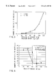
- FIG. 14 shows differences in cleaning effect where the water jetting position (L) was set to 7 mm or 11 mm in the Cavipen cleaning method.
- the diameter of the nozzle (D) was set to 0.3 mm
- the rotational speed of the wafer was set to 1,000 rpm
- the pressure (P) was set to 110 kgf/cm 2 .
- FIG. 19 shows the zeta potential dependency of the zeta potential of each of Si, SiO 2 and SiN films which was set forth in a publication, “Cleaning Technology of the Surface of Silicon Wafer” (Realize Co., Ltd., pp. 67, 1995, K. Kashiwagi et al).
- FIG. 20 shows the pH dependency of the zeta potential of each of SiO 2 and Al 2 O 3 films which was set forth in a publication, “Mechanical brush scrubbing for post-CMP clean”, Solid State Technology, pp. 109-114 (June, 1995), Wllbur C. Krusell, John M. de Larlos, Jackle Zhang.
- a rinsing water supply pipe 7 is protruded via a central portion of the top wall of the chamber 1 into the chamber 1 while ensuring an air-tightness between the top wall of the chamber 1 and the rinsing water supply pipe 7 , thereby making it possible to feed a rinsing water (ultrapure water) to the surface of the semiconductor substrate 20 .
- the pressure of a primary high pressure water to be jetted against the reverse surface of the semiconductor substrate 20 is proportional to the intensity of the impulse wave transmitted to the surface of the semiconductor substrate 20 (permeating secondary intensity), so that the intensity of the impulse wave can be controlled by means of the pressure of a primary high pressure water.
- the load lock portion is not required to be acid-resistive or alkali-resistive.
- a slidable portion located in the region lower than the semiconductor substrate is limited to a small region, the air-tightness of the slidable portion can be sufficiently ensured by making use of a Teflon seal, etc.
- FIG. 27 represents a schematic sectional view illustrating a first modified example of the semiconductor substrate cleaning apparatus.
- the substrate holder 2 is moved downward until the semiconductor substrate 20 is placed close to the tip end 4 A of the nozzle and at the same time, placed inside the cleaning tank 1 A.
- the substrate holder 2 is connected with a rotating mechanism (not shown) disposed outside the chamber 1 so as to allow the substrate holder 2 to rotate in situ.
- FIG. 30 shows the number of particles adhering on the surface of a semiconductor substrate which was cleaned according to the fourth embodiment of this invention, the result being shown in comparison with the results obtained using a conventional cleaning method and using the cleaning method according to the first embodiment of this invention.
- FIG. 31A shows a plan view of the nozzle tip end 4 A as well as a plan view of the nozzle frame 5 .
- the tip end 4 A of nozzle which is formed of a fine Teflon tube is protruded from a central portion of the cylindrical nozzle frame 5 .
- FIG. 31B shows a first modification of the tip end 4 A of nozzle as well as of the nozzle frame 5 .
- a plurality of nozzle tip ends 4 A are protruded from a rectangular parallelepiped nozzle frame 5 whose length approximately corresponds with the diameter of the semiconductor substrate to be cleaned.
Landscapes
- Engineering & Computer Science (AREA)
- Physics & Mathematics (AREA)
- Condensed Matter Physics & Semiconductors (AREA)
- General Physics & Mathematics (AREA)
- Manufacturing & Machinery (AREA)
- Computer Hardware Design (AREA)
- Microelectronics & Electronic Packaging (AREA)
- Power Engineering (AREA)
- Cleaning Or Drying Semiconductors (AREA)
- Cleaning By Liquid Or Steam (AREA)
Priority Applications (1)
| Application Number | Priority Date | Filing Date | Title |
|---|---|---|---|
| US10/179,885 US6673163B2 (en) | 1998-10-12 | 2002-06-26 | Apparatus and method for cleaning a semiconductor substrate |
Applications Claiming Priority (4)
| Application Number | Priority Date | Filing Date | Title |
|---|---|---|---|
| JP10-288579 | 1998-10-12 | ||
| JP28857998 | 1998-10-12 | ||
| JP24617699A JP3772056B2 (ja) | 1998-10-12 | 1999-08-31 | 半導体基板の洗浄方法 |
| JP11-246176 | 1999-08-31 |
Related Child Applications (1)
| Application Number | Title | Priority Date | Filing Date |
|---|---|---|---|
| US10/179,885 Division US6673163B2 (en) | 1998-10-12 | 2002-06-26 | Apparatus and method for cleaning a semiconductor substrate |
Publications (1)
| Publication Number | Publication Date |
|---|---|
| US6431185B1 true US6431185B1 (en) | 2002-08-13 |
Family
ID=26537604
Family Applications (2)
| Application Number | Title | Priority Date | Filing Date |
|---|---|---|---|
| US09/401,864 Expired - Fee Related US6431185B1 (en) | 1998-10-12 | 1999-09-22 | Apparatus and method for cleaning a semiconductor substrate |
| US10/179,885 Expired - Fee Related US6673163B2 (en) | 1998-10-12 | 2002-06-26 | Apparatus and method for cleaning a semiconductor substrate |
Family Applications After (1)
| Application Number | Title | Priority Date | Filing Date |
|---|---|---|---|
| US10/179,885 Expired - Fee Related US6673163B2 (en) | 1998-10-12 | 2002-06-26 | Apparatus and method for cleaning a semiconductor substrate |
Country Status (2)
| Country | Link |
|---|---|
| US (2) | US6431185B1 (ja) |
| JP (1) | JP3772056B2 (ja) |
Cited By (38)
| Publication number | Priority date | Publication date | Assignee | Title |
|---|---|---|---|---|
| US20030013310A1 (en) * | 2001-07-12 | 2003-01-16 | Nec Corporation | Method of washing a semiconductor wafer |
| US20030121528A1 (en) * | 1999-06-29 | 2003-07-03 | Intersil Americas Inc. | Brushless multipass silicon wafer cleaning process for post chemical mechanical polishing using immersion |
| US20030139046A1 (en) * | 2001-05-25 | 2003-07-24 | Mitsubishi Denki Kabushiki Kaisha | Method and apparatus for cleaning semiconductor device and method of fabricating semiconductor device |
| US6598805B2 (en) * | 2001-05-30 | 2003-07-29 | Dainippon Screen Mfg. Co., Ltd | Substrate cleaning apparatus |
| US6625568B2 (en) * | 2000-10-23 | 2003-09-23 | James Tyson | Sound-based vessel cleaner inspection |
| US20030184720A1 (en) * | 2002-01-18 | 2003-10-02 | Asml Netherlands, B.V. | Lithographic apparatus, apparatus cleaning method, device manufacturing method and device manufactured thereby |
| US20030196285A1 (en) * | 2002-04-19 | 2003-10-23 | Hyen-Ok O | Washing machine for sports shoes |
| US6679950B2 (en) * | 2000-06-29 | 2004-01-20 | Ebara Corporation | Cleaning method and cleaner |
| WO2004011161A2 (en) * | 2002-07-29 | 2004-02-05 | Brooks Automation, Inc. | Manipulating device for photomasks that provides possibilities for cleaning and inspection of photomasks |
| US20040029392A1 (en) * | 2002-08-08 | 2004-02-12 | Micron Technology, Inc. | Methods using a peroxide-generating compound to remove group VIII metal-containing residue |
| US20040025904A1 (en) * | 2002-08-08 | 2004-02-12 | Micron Technologies, Inc. | Methods and compositions for removing group VIII metal-containing materials from surfaces |
| US20040031503A1 (en) * | 2002-08-16 | 2004-02-19 | Dainippon Screen Mfg. Co., Ltd. | Substrate treatment apparatus and substrate treatment method |
| US6723655B2 (en) | 2001-06-29 | 2004-04-20 | Hynix Semiconductor Inc. | Methods for fabricating a semiconductor device |
| US20040087158A1 (en) * | 2002-10-29 | 2004-05-06 | Dainippon Screen Mfg. Co., Ltd. | Substrate processing method and substrate processing apparatus |
| WO2004082857A1 (en) * | 2003-03-12 | 2004-09-30 | Mattson Technology Inc. | Systems and methods for cleaning semiconductor substrates using a reduced volume of liquid |
| US20050040442A1 (en) * | 2003-08-21 | 2005-02-24 | Andreas Michael T. | Wafer cleaning method and resulting wafer |
| US20050227187A1 (en) * | 2002-03-04 | 2005-10-13 | Supercritical Systems Inc. | Ionic fluid in supercritical fluid for semiconductor processing |
| US20060102282A1 (en) * | 2004-11-15 | 2006-05-18 | Supercritical Systems, Inc. | Method and apparatus for selectively filtering residue from a processing chamber |
| US20060137715A1 (en) * | 2004-12-28 | 2006-06-29 | Dongbuanam Semiconductor Inc. | Cleaning method for removing copper-based foreign particles |
| US20060185694A1 (en) * | 2005-02-23 | 2006-08-24 | Richard Brown | Rinsing step in supercritical processing |
| US20060185693A1 (en) * | 2005-02-23 | 2006-08-24 | Richard Brown | Cleaning step in supercritical processing |
| US20060213536A1 (en) * | 2005-03-28 | 2006-09-28 | Dainippon Screen Mfg. Co., Ltd. | Substrate cleaning apparatus and substrate cleaning method |
| US20060213820A1 (en) * | 2005-03-23 | 2006-09-28 | Bertram Ronald T | Removal of contaminants from a fluid |
| US20060219268A1 (en) * | 2005-03-30 | 2006-10-05 | Gunilla Jacobson | Neutralization of systemic poisoning in wafer processing |
| US20060223899A1 (en) * | 2005-03-30 | 2006-10-05 | Hillman Joseph T | Removal of porogens and porogen residues using supercritical CO2 |
| US20060226117A1 (en) * | 2005-03-29 | 2006-10-12 | Bertram Ronald T | Phase change based heating element system and method |
| US20060228874A1 (en) * | 2005-03-30 | 2006-10-12 | Joseph Hillman | Method of inhibiting copper corrosion during supercritical CO2 cleaning |
| US20060225811A1 (en) * | 2005-03-30 | 2006-10-12 | Alexei Sheydayi | Gate valve for plus-atmospheric pressure semiconductor process vessels |
| US20060225769A1 (en) * | 2005-03-30 | 2006-10-12 | Gentaro Goshi | Isothermal control of a process chamber |
| US20070000519A1 (en) * | 2005-06-30 | 2007-01-04 | Gunilla Jacobson | Removal of residues for low-k dielectric materials in wafer processing |
| US7250087B1 (en) | 2006-05-16 | 2007-07-31 | James Tyson | Clogged nozzle detection |
| US20090056744A1 (en) * | 2007-08-29 | 2009-03-05 | Micron Technology, Inc. | Wafer cleaning compositions and methods |
| US20090199358A1 (en) * | 2008-02-07 | 2009-08-13 | Fuji Paudal Co., Ltd. | Cleaning device and fine-particle processing device therewith |
| US20100155907A1 (en) * | 2008-12-23 | 2010-06-24 | Soendker Erich H | Semiconductor device having an inorganic coating layer applied over a junction termination extension |
| US7767145B2 (en) | 2005-03-28 | 2010-08-03 | Toyko Electron Limited | High pressure fourier transform infrared cell |
| US20100300491A1 (en) * | 2009-06-01 | 2010-12-02 | Micron Technology, Inc. | Wafer cleaning with immersed stream or spray nozzle |
| US9090854B2 (en) | 2011-10-25 | 2015-07-28 | Lam Research Ag | Method and apparatus for processing wafer-shaped articles |
| CN108496246A (zh) * | 2016-01-27 | 2018-09-04 | 应用材料公司 | 狭缝阀门涂层及用于清洁狭缝阀门的方法 |
Families Citing this family (14)
| Publication number | Priority date | Publication date | Assignee | Title |
|---|---|---|---|---|
| JP2002292346A (ja) * | 2001-03-29 | 2002-10-08 | Sharp Corp | 付着膜回収装置および付着膜の回収方法 |
| US20030217762A1 (en) * | 2002-02-18 | 2003-11-27 | Lam Research Corporation | Water supply apparatus and method thereof |
| US6955485B2 (en) * | 2002-03-01 | 2005-10-18 | Tokyo Electron Limited | Developing method and developing unit |
| KR100582202B1 (ko) * | 2003-10-13 | 2006-05-23 | 엘지.필립스 엘시디 주식회사 | 박막트랜지스터 어레이 기판의 제조장치 및 방법 |
| US7611589B2 (en) * | 2005-03-04 | 2009-11-03 | Taiwan Semiconductor Manufacturing Co., Ltd. | Methods of spin-on wafer cleaning |
| JP5038695B2 (ja) * | 2006-11-30 | 2012-10-03 | 東京応化工業株式会社 | 処理装置および表面処理治具 |
| JP2010519722A (ja) * | 2007-02-23 | 2010-06-03 | 株式会社ニコン | 露光方法、露光装置、デバイス製造方法、及び液浸露光用基板 |
| JP5404093B2 (ja) * | 2008-03-31 | 2014-01-29 | 株式会社東芝 | 半導体ウェーハの洗浄方法 |
| JP5317529B2 (ja) * | 2008-05-02 | 2013-10-16 | Sumco Techxiv株式会社 | 半導体ウェーハの処理方法及び処理装置 |
| JPWO2011135979A1 (ja) * | 2010-04-28 | 2013-07-18 | コニカミノルタ株式会社 | 撮像用レンズの製造方法 |
| JP5945178B2 (ja) * | 2012-07-04 | 2016-07-05 | 東京エレクトロン株式会社 | ガスクラスター照射機構およびそれを用いた基板処理装置、ならびにガスクラスター照射方法 |
| JP6432858B2 (ja) * | 2014-07-18 | 2018-12-05 | 株式会社Screenホールディングス | 基板処理装置 |
| JP6387329B2 (ja) * | 2015-08-20 | 2018-09-05 | 東京エレクトロン株式会社 | 基板処理装置およびノズル洗浄方法 |
| KR102571748B1 (ko) * | 2021-05-04 | 2023-08-25 | 세메스 주식회사 | 기판 처리 장치 및 방법 |
Citations (8)
| Publication number | Priority date | Publication date | Assignee | Title |
|---|---|---|---|---|
| JPH03148825A (ja) | 1989-11-06 | 1991-06-25 | Ebara Corp | ジェットスクラバー |
| US5468302A (en) * | 1994-07-13 | 1995-11-21 | Thietje; Jerry | Semiconductor wafer cleaning system |
| JPH0852443A (ja) | 1994-08-11 | 1996-02-27 | Ebara Corp | 超純水による洗浄方法 |
| US5540245A (en) * | 1994-03-22 | 1996-07-30 | Shin-Etsu Handotai Co., Ltd. | Processing equipment of single substrate transfer type |
| US5562778A (en) * | 1993-12-17 | 1996-10-08 | International Business Machines Corporation | Ultrasonic jet semiconductor wafer cleaning method |
| US5868866A (en) * | 1995-03-03 | 1999-02-09 | Ebara Corporation | Method of and apparatus for cleaning workpiece |
| US6175983B1 (en) * | 1998-01-06 | 2001-01-23 | Tokyo Electron Limited | Substrate washing apparatus and method |
| JP3148825B1 (ja) | 1999-10-12 | 2001-03-26 | エスエムケイ株式会社 | 多連型ネジ式ターミナル装置 |
Family Cites Families (9)
| Publication number | Priority date | Publication date | Assignee | Title |
|---|---|---|---|---|
| US4827867A (en) * | 1985-11-28 | 1989-05-09 | Daikin Industries, Ltd. | Resist developing apparatus |
| JPH06459A (ja) * | 1992-06-19 | 1994-01-11 | T H I Syst Kk | 洗浄乾燥方法とその装置 |
| US5518542A (en) * | 1993-11-05 | 1996-05-21 | Tokyo Electron Limited | Double-sided substrate cleaning apparatus |
| US5520205A (en) * | 1994-07-01 | 1996-05-28 | Texas Instruments Incorporated | Apparatus for wafer cleaning with rotation |
| US5762084A (en) * | 1994-07-15 | 1998-06-09 | Ontrak Systems, Inc. | Megasonic bath |
| JP3278590B2 (ja) * | 1996-08-23 | 2002-04-30 | 株式会社東芝 | 超音波洗浄装置及び超音波洗浄方法 |
| US6413355B1 (en) * | 1996-09-27 | 2002-07-02 | Tokyo Electron Limited | Apparatus for and method of cleaning objects to be processed |
| AU6327398A (en) * | 1997-02-18 | 1998-09-08 | Scp Global Technologies | Multiple stage wet processing chamber |
| US6070284A (en) * | 1998-02-04 | 2000-06-06 | Silikinetic Technology, Inc. | Wafer cleaning method and system |
-
1999
- 1999-08-31 JP JP24617699A patent/JP3772056B2/ja not_active Expired - Fee Related
- 1999-09-22 US US09/401,864 patent/US6431185B1/en not_active Expired - Fee Related
-
2002
- 2002-06-26 US US10/179,885 patent/US6673163B2/en not_active Expired - Fee Related
Patent Citations (8)
| Publication number | Priority date | Publication date | Assignee | Title |
|---|---|---|---|---|
| JPH03148825A (ja) | 1989-11-06 | 1991-06-25 | Ebara Corp | ジェットスクラバー |
| US5562778A (en) * | 1993-12-17 | 1996-10-08 | International Business Machines Corporation | Ultrasonic jet semiconductor wafer cleaning method |
| US5540245A (en) * | 1994-03-22 | 1996-07-30 | Shin-Etsu Handotai Co., Ltd. | Processing equipment of single substrate transfer type |
| US5468302A (en) * | 1994-07-13 | 1995-11-21 | Thietje; Jerry | Semiconductor wafer cleaning system |
| JPH0852443A (ja) | 1994-08-11 | 1996-02-27 | Ebara Corp | 超純水による洗浄方法 |
| US5868866A (en) * | 1995-03-03 | 1999-02-09 | Ebara Corporation | Method of and apparatus for cleaning workpiece |
| US6175983B1 (en) * | 1998-01-06 | 2001-01-23 | Tokyo Electron Limited | Substrate washing apparatus and method |
| JP3148825B1 (ja) | 1999-10-12 | 2001-03-26 | エスエムケイ株式会社 | 多連型ネジ式ターミナル装置 |
Non-Patent Citations (3)
| Title |
|---|
| Hymes et al., Brush Scrubbing Emerges As Future Wafer-Cleaning Technology, Jul. 1, 1997, Internet, vol. 40, pp. 1-9.* * |
| Krusell et al., "Mechanical Brush Scrubbing for Post-CMP Clean," Solid State Technology, pp. 109-114 (1995). |
| Nadahara, S., "Cavitation Jet Cleaning After CMP", the 2nd International CMP Symposium, pp. 277-280, (1996). |
Cited By (56)
| Publication number | Priority date | Publication date | Assignee | Title |
|---|---|---|---|---|
| US20030121528A1 (en) * | 1999-06-29 | 2003-07-03 | Intersil Americas Inc. | Brushless multipass silicon wafer cleaning process for post chemical mechanical polishing using immersion |
| US6679950B2 (en) * | 2000-06-29 | 2004-01-20 | Ebara Corporation | Cleaning method and cleaner |
| US6625568B2 (en) * | 2000-10-23 | 2003-09-23 | James Tyson | Sound-based vessel cleaner inspection |
| US20030139046A1 (en) * | 2001-05-25 | 2003-07-24 | Mitsubishi Denki Kabushiki Kaisha | Method and apparatus for cleaning semiconductor device and method of fabricating semiconductor device |
| US6598805B2 (en) * | 2001-05-30 | 2003-07-29 | Dainippon Screen Mfg. Co., Ltd | Substrate cleaning apparatus |
| US6723655B2 (en) | 2001-06-29 | 2004-04-20 | Hynix Semiconductor Inc. | Methods for fabricating a semiconductor device |
| US6864187B2 (en) * | 2001-07-12 | 2005-03-08 | Nec Electronics Corporation | Method of washing a semiconductor wafer |
| US20030013310A1 (en) * | 2001-07-12 | 2003-01-16 | Nec Corporation | Method of washing a semiconductor wafer |
| US20030184720A1 (en) * | 2002-01-18 | 2003-10-02 | Asml Netherlands, B.V. | Lithographic apparatus, apparatus cleaning method, device manufacturing method and device manufactured thereby |
| US6856376B2 (en) * | 2002-01-18 | 2005-02-15 | Asml Netherlands B.V. | Lithographic apparatus, apparatus cleaning method, device manufacturing method and device manufactured thereby |
| US20050227187A1 (en) * | 2002-03-04 | 2005-10-13 | Supercritical Systems Inc. | Ionic fluid in supercritical fluid for semiconductor processing |
| US20030196285A1 (en) * | 2002-04-19 | 2003-10-23 | Hyen-Ok O | Washing machine for sports shoes |
| US20040111823A1 (en) * | 2002-07-29 | 2004-06-17 | Jakob Blattner | Manipulating device for photomasks that provides possibilities for cleaning and inspection of photomasks |
| US7478454B2 (en) | 2002-07-29 | 2009-01-20 | Brooks Automation, Inc. | Manipulating device for photomasks that provides possibilities for cleaning and inspection of photomasks |
| WO2004011161A2 (en) * | 2002-07-29 | 2004-02-05 | Brooks Automation, Inc. | Manipulating device for photomasks that provides possibilities for cleaning and inspection of photomasks |
| WO2004011161A3 (en) * | 2002-07-29 | 2005-04-21 | Brooks Automation Inc | Manipulating device for photomasks that provides possibilities for cleaning and inspection of photomasks |
| US20040025904A1 (en) * | 2002-08-08 | 2004-02-12 | Micron Technologies, Inc. | Methods and compositions for removing group VIII metal-containing materials from surfaces |
| US20040029392A1 (en) * | 2002-08-08 | 2004-02-12 | Micron Technology, Inc. | Methods using a peroxide-generating compound to remove group VIII metal-containing residue |
| US20060201913A1 (en) * | 2002-08-08 | 2006-09-14 | Micron Technology, Inc. | Methods and compositions for removing Group VIII metal-containing materials from surfaces |
| US6905974B2 (en) * | 2002-08-08 | 2005-06-14 | Micron Technology, Inc. | Methods using a peroxide-generating compound to remove group VIII metal-containing residue |
| US7077975B2 (en) | 2002-08-08 | 2006-07-18 | Micron Technology, Inc. | Methods and compositions for removing group VIII metal-containing materials from surfaces |
| US20050217696A1 (en) * | 2002-08-08 | 2005-10-06 | Micron Technology, Inc. | Methods using a peroxide-generating compound to remove group VIII metal-containing residue |
| US20040031503A1 (en) * | 2002-08-16 | 2004-02-19 | Dainippon Screen Mfg. Co., Ltd. | Substrate treatment apparatus and substrate treatment method |
| US7494549B2 (en) * | 2002-08-16 | 2009-02-24 | Dainippon Screen Mfg. Co., Ltd. | Substrate treatment apparatus and substrate treatment method |
| US20040087158A1 (en) * | 2002-10-29 | 2004-05-06 | Dainippon Screen Mfg. Co., Ltd. | Substrate processing method and substrate processing apparatus |
| US7524771B2 (en) * | 2002-10-29 | 2009-04-28 | Dainippon Screen Mfg. Co., Ltd. | Substrate processing method using alkaline solution and acid solution |
| WO2004082857A1 (en) * | 2003-03-12 | 2004-09-30 | Mattson Technology Inc. | Systems and methods for cleaning semiconductor substrates using a reduced volume of liquid |
| US20050040443A1 (en) * | 2003-08-21 | 2005-02-24 | Andreas Michael T. | Wafer cleaning method and resulting wafer |
| US6930017B2 (en) | 2003-08-21 | 2005-08-16 | Micron Technology, Inc. | Wafer Cleaning method and resulting wafer |
| US7023099B2 (en) | 2003-08-21 | 2006-04-04 | Micron Technology, Inc | Wafer cleaning method and resulting wafer |
| US20050040442A1 (en) * | 2003-08-21 | 2005-02-24 | Andreas Michael T. | Wafer cleaning method and resulting wafer |
| US20060102282A1 (en) * | 2004-11-15 | 2006-05-18 | Supercritical Systems, Inc. | Method and apparatus for selectively filtering residue from a processing chamber |
| US20060137715A1 (en) * | 2004-12-28 | 2006-06-29 | Dongbuanam Semiconductor Inc. | Cleaning method for removing copper-based foreign particles |
| US20060185694A1 (en) * | 2005-02-23 | 2006-08-24 | Richard Brown | Rinsing step in supercritical processing |
| US20060185693A1 (en) * | 2005-02-23 | 2006-08-24 | Richard Brown | Cleaning step in supercritical processing |
| US20060213820A1 (en) * | 2005-03-23 | 2006-09-28 | Bertram Ronald T | Removal of contaminants from a fluid |
| US20060213536A1 (en) * | 2005-03-28 | 2006-09-28 | Dainippon Screen Mfg. Co., Ltd. | Substrate cleaning apparatus and substrate cleaning method |
| US7767145B2 (en) | 2005-03-28 | 2010-08-03 | Toyko Electron Limited | High pressure fourier transform infrared cell |
| US20060226117A1 (en) * | 2005-03-29 | 2006-10-12 | Bertram Ronald T | Phase change based heating element system and method |
| US20060225769A1 (en) * | 2005-03-30 | 2006-10-12 | Gentaro Goshi | Isothermal control of a process chamber |
| US20060219268A1 (en) * | 2005-03-30 | 2006-10-05 | Gunilla Jacobson | Neutralization of systemic poisoning in wafer processing |
| US20060225811A1 (en) * | 2005-03-30 | 2006-10-12 | Alexei Sheydayi | Gate valve for plus-atmospheric pressure semiconductor process vessels |
| US20060228874A1 (en) * | 2005-03-30 | 2006-10-12 | Joseph Hillman | Method of inhibiting copper corrosion during supercritical CO2 cleaning |
| US20060223899A1 (en) * | 2005-03-30 | 2006-10-05 | Hillman Joseph T | Removal of porogens and porogen residues using supercritical CO2 |
| US20070000519A1 (en) * | 2005-06-30 | 2007-01-04 | Gunilla Jacobson | Removal of residues for low-k dielectric materials in wafer processing |
| US7250087B1 (en) | 2006-05-16 | 2007-07-31 | James Tyson | Clogged nozzle detection |
| US20090056744A1 (en) * | 2007-08-29 | 2009-03-05 | Micron Technology, Inc. | Wafer cleaning compositions and methods |
| US20090199358A1 (en) * | 2008-02-07 | 2009-08-13 | Fuji Paudal Co., Ltd. | Cleaning device and fine-particle processing device therewith |
| US8308469B2 (en) * | 2008-02-07 | 2012-11-13 | Fuji Paudal Conmpany Limited | Cleaning device and fine-particle processing device therewith |
| US20100155907A1 (en) * | 2008-12-23 | 2010-06-24 | Soendker Erich H | Semiconductor device having an inorganic coating layer applied over a junction termination extension |
| US8106487B2 (en) | 2008-12-23 | 2012-01-31 | Pratt & Whitney Rocketdyne, Inc. | Semiconductor device having an inorganic coating layer applied over a junction termination extension |
| US20100300491A1 (en) * | 2009-06-01 | 2010-12-02 | Micron Technology, Inc. | Wafer cleaning with immersed stream or spray nozzle |
| US8454760B2 (en) * | 2009-06-01 | 2013-06-04 | Micron Technology, Inc. | Wafer cleaning with immersed stream or spray nozzle |
| US9090854B2 (en) | 2011-10-25 | 2015-07-28 | Lam Research Ag | Method and apparatus for processing wafer-shaped articles |
| CN108496246A (zh) * | 2016-01-27 | 2018-09-04 | 应用材料公司 | 狭缝阀门涂层及用于清洁狭缝阀门的方法 |
| CN108496246B (zh) * | 2016-01-27 | 2023-07-21 | 应用材料公司 | 狭缝阀门涂层及用于清洁狭缝阀门的方法 |
Also Published As
| Publication number | Publication date |
|---|---|
| US20020170572A1 (en) | 2002-11-21 |
| JP2000188273A (ja) | 2000-07-04 |
| US6673163B2 (en) | 2004-01-06 |
| JP3772056B2 (ja) | 2006-05-10 |
Similar Documents
| Publication | Publication Date | Title |
|---|---|---|
| US6431185B1 (en) | Apparatus and method for cleaning a semiconductor substrate | |
| JP4481394B2 (ja) | 半導体基板の洗浄装置及びその洗浄方法 | |
| US20190088510A1 (en) | Substrate cleaning device, substrate cleaning method, substrate processing device, and substrate drying device | |
| US20010002593A1 (en) | Method and apparatus for cleaning the edge of a thin disc | |
| US10737301B2 (en) | Substrate cleaning apparatus | |
| JPWO2007108315A1 (ja) | 基板処理装置及び基板処理方法 | |
| JP3786651B2 (ja) | 機械化学研磨後の汚染物質を除去する方法 | |
| JP2021185628A (ja) | 超音波洗浄装置および洗浄具のクリーニング装置 | |
| US20020062839A1 (en) | Method and apparatus for frontside and backside wet processing of a wafer | |
| US20120298158A1 (en) | Microelectronic substrate cleaning systems with polyelectrolyte and associated methods | |
| TW201914701A (zh) | 用於清潔晶圓的方法 | |
| JP2010021457A (ja) | ブラシの洗浄方法 | |
| US9640384B2 (en) | Substrate cleaning apparatus and substrate cleaning method | |
| JP2017183553A (ja) | 基板洗浄装置及び基板処理装置 | |
| US20070017547A1 (en) | Method for cleaning disk-shape glass substrate and magnetic disk | |
| KR102098992B1 (ko) | 웨이퍼 폴리싱 패드의 세정 장치 | |
| JP2015099852A (ja) | 基板洗浄装置および基板処理装置 | |
| KR20100005571A (ko) | 패드 컨디셔닝 유닛 및 이를 구비한 매엽식 기판 연마장치와, 패드 컨디셔닝 방법 | |
| KR20140086846A (ko) | 기판 세정 장치 및 기판 세정 방법 | |
| KR20230034741A (ko) | 기판 처리 장치 및 방법 | |
| JP2003318148A (ja) | 基板洗浄装置および基板洗浄方法 | |
| US20240258125A1 (en) | Electronic component cleaning apparatus | |
| KR20090069380A (ko) | Hf 모듈을 구비한 스크러버 및 이를 이용한 웨이퍼세정방법 | |
| JP2017163017A (ja) | 基板処理装置 | |
| KR20190083599A (ko) | 기판 처리 시스템 및 기판 처리 방법 |
Legal Events
| Date | Code | Title | Description |
|---|---|---|---|
| AS | Assignment |
Owner name: KABUSHIKI KAISHA TOSHIBA, JAPAN Free format text: ASSIGNMENT OF ASSIGNORS INTEREST;ASSIGNORS:TOMITA, HIROSHI;NADAHARA, SOICHI;SATO, MOTOYUKI;REEL/FRAME:010279/0116 Effective date: 19990916 |
|
| FPAY | Fee payment |
Year of fee payment: 4 |
|
| FEPP | Fee payment procedure |
Free format text: PAYOR NUMBER ASSIGNED (ORIGINAL EVENT CODE: ASPN); ENTITY STATUS OF PATENT OWNER: LARGE ENTITY |
|
| FPAY | Fee payment |
Year of fee payment: 8 |
|
| REMI | Maintenance fee reminder mailed | ||
| LAPS | Lapse for failure to pay maintenance fees | ||
| STCH | Information on status: patent discontinuation |
Free format text: PATENT EXPIRED DUE TO NONPAYMENT OF MAINTENANCE FEES UNDER 37 CFR 1.362 |
|
| FP | Lapsed due to failure to pay maintenance fee |
Effective date: 20140813 |