US6388306B1 - Semiconductor device with rapid reverse recovery characteristic - Google Patents
Semiconductor device with rapid reverse recovery characteristic Download PDFInfo
- Publication number
- US6388306B1 US6388306B1 US09/619,316 US61931600A US6388306B1 US 6388306 B1 US6388306 B1 US 6388306B1 US 61931600 A US61931600 A US 61931600A US 6388306 B1 US6388306 B1 US 6388306B1
- Authority
- US
- United States
- Prior art keywords
- layer
- semiconductor layer
- voltage
- semiconductor
- main electrode
- Prior art date
- Legal status (The legal status is an assumption and is not a legal conclusion. Google has not performed a legal analysis and makes no representation as to the accuracy of the status listed.)
- Expired - Fee Related, expires
Links
Images


Classifications
-
- H—ELECTRICITY
- H10—SEMICONDUCTOR DEVICES; ELECTRIC SOLID-STATE DEVICES NOT OTHERWISE PROVIDED FOR
- H10D—INORGANIC ELECTRIC SEMICONDUCTOR DEVICES
- H10D8/00—Diodes
- H10D8/80—PNPN diodes, e.g. Shockley diodes or break-over diodes
-
- H—ELECTRICITY
- H10—SEMICONDUCTOR DEVICES; ELECTRIC SOLID-STATE DEVICES NOT OTHERWISE PROVIDED FOR
- H10D—INORGANIC ELECTRIC SEMICONDUCTOR DEVICES
- H10D8/00—Diodes
Definitions
- the present invention relates to semiconductor devices such as a diode having a PN junction which is required to provide a high breakdown voltage and a rapid reverse recovery characteristic.
- Diodes are required to provide a high breakdown voltage and a rapid reverse recovery characteristic as flow-back diodes or voltage-clamping diodes needed in applications of high-voltage switching device such as IGBTs (Insulated Gate Bipolar Transistors) and GCTs (Gate Commutated Turn-off Thyristors).
- IGBTs Insulated Gate Bipolar Transistors
- GCTs Gate Commutated Turn-off Thyristors
- FIG. 13 is a cross-sectional view showing a sectional structure of a conventional common diode which meets the needs stated above.
- an N ⁇ layer 601 as a semiconductor substrate of silicon etc. is formed on an N + layer 603 and a P layer 602 is formed on the N ⁇ layer 601 .
- the concentration of N-type impurity is higher in the N + layer 603 than in the N ⁇ layer 601 .
- An anode electrode 604 made of a low-resistant metal is formed on the P layer 602 and a cathode electrode 605 made of a low-resistant metal as well as the anode electrode 604 is formed under the N + layer 603 .
- the lifetime in the vicinity of the PN junction is controlled by proton irradiation etc. and a center of carrier recombination is formed.
- the lifetime in the entire semiconductor substrate is controlled and shortened by techniques such as diffusion of precious metal, irradiation of electron beam, etc.
- the lifetime in the vicinity of the PN junction is locally controlled and shortened to realize characteristics of low forward voltage, small reverse recovery current (the peak value of the reverse current) and high di/dt strength (the maximum value of the current decreasing rate di/dt which can be given without damaging the diode).
- a diode in the reverse recovery operation has a capacitance component defined by the depletion layer and excess carriers as parameters and a resistance component defined by the applied voltage, leakage current and recombination current of the excess carries as parameters.
- the resistance component, the capacitance component and the inductance component of the external circuit for applying the reverse voltage form an LCR series circuit.
- the capacitance component and the resistance component of the diode vary with time.
- the resistance component rapidly increases when the excess carriers outside the depletion layer have disappeared, and the natural oscillation condition of the LCR series circuit is reached and voltage oscillation occurs.
- the resistance component rapidly varies to cause voltage oscillation also when the depletion layer reaches the N + layer 603 .
- a semiconductor device comprises: a first conductivity type first semiconductor layer; a first conductivity type second semiconductor layer being formed on the first semiconductor layer, the second semiconductor layer having a lower impurity concentration of the first conductivity type than the first semiconductor layer; a second conductivity type third semiconductor layer being formed on the second semiconductor layer; a first main electrode formed over the third semiconductor layer; and a second main electrode formed under the first semiconductor layer; wherein the film thickness of the second semiconductor layer is set to satisfy both of a first condition that a depletion layer extending from a PN junction at an interface between the second semiconductor layer and the third semiconductor layer does not reach the first semiconductor layer when a reverse voltage of about 1 ⁇ 2 to 2 ⁇ 3 of the reverse-direction voltage blocking capability of the PN junction is applied to the first and second main electrodes, and a second condition that the depletion layer extending from the PN junction reaches the first semiconductor layer when a reverse voltage exceeding about 2 ⁇ 3 of the voltage blocking capability is applied to the first and second main electrodes.
- the first main electrode includes a main electrode formed directly on the third semiconductor layer
- the second main electrode comprises a main electrode formed directly on the underside of the first semiconductor layer
- the semiconductor device further comprises: a second conductivity type fourth semiconductor layer being formed under the first semiconductor layer, and wherein the first main electrode includes a main electrode formed directly on the third semiconductor layer and the second main electrode includes a main electrode formed directly on the underside of the fourth semiconductor layer.
- the semiconductor device further comprises: a second conductivity type fourth semiconductor layer being formed under the first semiconductor layer; and a first conductivity type fifth semiconductor layer being formed on the third semiconductor layer, and wherein the first main electrode includes a main electrode formed directly on the fifth semiconductor layer and the second main electrode includes a main electrode formed directly on the underside of the fourth semiconductor layer.
- the third semiconductor layer comprises a plurality of semiconductor regions formed selectively in a surface of the second semiconductor layer
- the first main electrode comprises a plurality of partial electrodes formed on the plurality of semiconductor regions, respectively.
- the lifetime in the vicinity of the interface between the second and third semiconductor layers is set shorter than the lifetime in the vicinity of the interface between the first and second semiconductor layers.
- the second condition includes a condition that the depletion layer extending from the PN junction reaches the first semiconductor layer when a reverse voltage equivalent to the voltage blocking capability is applied to the first and second main electrodes.
- the impurity concentration of the second semiconductor layer is set to satisfy a third condition that electric field which acts on the depletion layer when a reverse bias voltage equivalent to the voltage blocking capability is set is at an actual use level not more than a predetermined field strength.
- the first conductivity type includes N type and the second conductivity type includes P type.
- the film thickness of the second semiconductor layer is set to satisfy the first condition. Accordingly, it is possible to certainly suppress the voltage oscillation which would occur as the depletion layer reaches the first semiconductor layer when a reverse voltage of about 1 ⁇ 2 to 2 ⁇ 3 of the voltage blocking capability, which is generally used in the reverse recovery operation, is applied.
- the film thickness of the second semiconductor layer is set to also satisfy the second condition, so that the on-state voltage can be maintained low at an appropriate level.
- the semiconductor device of the second aspect provides a diode which can achieve well-balanced on-state voltage reduction and voltage oscillation suppression.
- the semiconductor device of the third aspect provides a transistor which can achieve well-balanced on-state voltage reduction and voltage oscillation suppression.
- the semiconductor device of the fourth aspect provides a thyristor which can achieve well-balanced on-state voltage reduction and voltage oscillation suppression.
- the plurality of semiconductor regions form PN junctions on their respective sides with the first semiconductor layer, which provides a diode with improved breakdown voltage.
- setting the lifetime short in the vicinity of the interface between the second and third semiconductor layers (in the vicinity of the PN junction) suppresses expansion of the depletion layer from the PN junction, which allows the second semiconductor layer to be formed thinner.
- the semiconductor device of the seventh aspect uses a voltage equivalent to the voltage blocking capability as the reverse voltage for the second condition, which provides a structure adapted to actual design.
- the impurity concentration of the second semiconductor layer is set so that the electric field which acts on the depletion layer is at an actual use level not higher than a predetermined field strength when a reverse bias voltage corresponding to the voltage blocking capability is set, and therefore no problem is encountered in actual operation.
- the present invention has been made to solve the problem above, and an object of the invention is to obtain a semiconductor device having a PN junction which can suppress voltage oscillation without causing any adverse effects.
- FIG. 1 is a graph showing the relation between the film thickness of the N ⁇ layer in a structure of the invention and the on-state voltage.
- FIG. 2 is a graph showing the percentage of expansion of the depletion layer in the N ⁇ layer and the magnitude of voltage oscillation, where a reverse voltage exceeding 2 ⁇ 3 of the voltage blocking capability is applied.
- FIG. 3 is a waveform diagram showing a variation of the reverse bias voltage in a diode during a reverse recovery operation.
- FIG. 4 is an explanation diagram showing a feature of the structure of the invention.
- FIG. 5 is an explanation diagram showing a feature of a diode having a conventional PIN structure.
- FIG. 6 is an explanation diagram showing a feature of a diode having a PN junction structure.
- FIG. 7 is a graph showing the percentage of on-state voltage and the percentage of voltage oscillation in the structure of the invention, PIN structure and PN junction structure.
- FIG. 8 is a cross-sectional view showing the structure of a semiconductor device according to a first preferred embodiment of the invention.
- FIG. 9 is a cross-sectional view showing the structure of a semiconductor device according to a second preferred embodiment of the invention.
- FIG. 10 is a cross-sectional view showing the structure of a semiconductor device according to a third preferred embodiment of the invention.
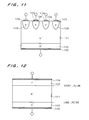
- FIG. 11 is a cross-sectional view showing the structure of a semiconductor device according to a fourth preferred embodiment of the invention.
- FIG. 12 is a cross-sectional view showing the structure of a semiconductor device according to a fifth preferred embodiment of the invention.
- FIG. 13 is a cross-sectional view showing a sectional structure of a conventional common diode.
- the basic structure of the invention is a three-layer structure of a P layer, an N ⁇ layer and an N ⁇ layer.
- the P layer 102 , N ⁇ layer 101 and N + layer 103 shown in FIG. 8 correspond to the P layer, N ⁇ layer and N + layer, respectively.
- This voltage oscillation can be prevented by increasing the film thickness of the N ⁇ layer in the basic structure so that the depletion layer expanding in the N ⁇ layer from the PN junction between the P layer and the N ⁇ layer will not reach the N + layer.
- the film thickness of the N ⁇ layer becomes large and causes an increase in the on-state voltage.
- a PIN structure with a small wafer thickness provides a low on-state voltage but it cannot avoid very large voltage oscillation since the depletion layer reaches the N + layer in the reverse recovery operation.
- the present invention intends to obtain a basic structure which can desirably balance the reduction of on-state voltage and the suppression of voltage oscillation. It was found that the film thickness of the N ⁇ layer in the diode portion having the basic structure shall be set so that the depletion layer expanding in the N ⁇ layer from the PN junction between the P layer and the N ⁇ layer does not reach the N + layer when a reverse voltage corresponding to about 1 ⁇ 2 to 2 ⁇ 3 of the voltage blocking capability is applied and so that the depletion layer reaches the N + layer when a reverse voltage exceeding about. 2 ⁇ 3 of the voltage blocking capability is applied.
- FIG. 1 is a graph showing the relation between the film thickness of the N ⁇ layer and the on-state voltage in the structure of the invention.
- the film thickness of the N ⁇ layer which is set according to the invention is taken as “1” (this film thickness is referred to as “set film thickness”hereinafter).
- set film thickness this film thickness is referred to as “set film thickness”hereinafter.
- the on-state voltage rises when the film thickness of the N ⁇ layer becomes thicker over the set film thickness; when it is set twice the set film thickness, for example, the on-state voltage increases by as much as about 0.8 V.
- the film thickness of the N ⁇ layer becomes thinner than the set film thickness the on-voltage decreases. However, it decreases just at a small rate; the on-state voltage decreases by only about 0.1 to 0.2 V even when the thickness is set at half of the set film thickness, for example.
- the depletion layer expanding from the PN junction does not reach the N + layer, so that the magnitude of the voltage oscillation can be suppressed to almost zero.
- FIG. 2 is a graph showing the percentage of the expansion of the depletion layer in the N ⁇ layer and the magnitude of the voltage oscillation, where a reverse voltage exceeding about 2 ⁇ 3 of the voltage blocking capability is applied. As shown in this diagram, when a reverse voltage exceeding about 2 ⁇ 3 of the voltage blocking capability is applied and the depletion layer reaches the N + layer and expands in the N + layer, the magnitude of the voltage oscillation is kept within the permissible range largely under 2 KV.
- FIG. 3 is a waveform diagram showing an example of setting of the reverse bias in the reverse recovery operation.
- a reverse bias is applied in a state in which a constant voltage of about 1 to 2 V is applied to the diode and a forward current is flowing.
- the peak value is set at about 2 ⁇ 3 of the voltage blocking capability and the steady-state voltage is set at about 1 ⁇ 2.
- the peak value is around ⁇ 3 KV corresponding to about 2 ⁇ 3 thereof and the steady-state voltage is ⁇ 2.25 KV corresponding to about 1 ⁇ 2.
- the present invention sets the film thickness of the N ⁇ layer in the basic-structure diode portion so that the following two conditions are both satisfied: a first condition that the depletion layer expanding in the N ⁇ layer does not reach the N + layer when a reverse voltage corresponding to about 1 ⁇ 2 to 2 ⁇ 3 of the voltage blocking capability is applied, and a second condition that the depletion layer reaches the N + layer when a reverse voltage exceeding about 2 ⁇ 3 of the voltage blocking capability is applied.
- the film thickness of the N ⁇ layer satisfies the first condition so that the depletion layer expanding in the N ⁇ layer does not reach the N + layer in this period. Accordingly, it is possible to effectively suppress the voltage oscillation as stated above.
- the film thickness of the N ⁇ layer is set thin enough to satisfy the second condition, so that the on-state voltage can be set at an appropriate low level.
- the impurity concentration (specific resistance) of the N ⁇ layer is set to satisfy a third condition that the electric field which acts on the depletion layer is at an actual use level not more than the maximum field strength of silicon (the maximum value of the field strength that silicon can withstand) when the reverse bias voltage is set at about ⁇ fraction (1/1) ⁇ of the voltage blocking capability.
- the impurity concentration and the film thickness of the N ⁇ layer are determined considering mutual relations between the first to third conditions, since the impurity concentration of the N ⁇ layer is related to the expansion of the depletion layer.
- FIG. 4 is an explanation diagram showing a feature of the structure of the invention.
- the present invention adopts a three-layer structure of the P layer 102 , N ⁇ layer 101 and N + layer 103 as the basic structure, which exhibits the electric field distribution shown as L 1 where the depletion layer forming from the PN junction between the N ⁇ layer 101 and the P layer 102 does not reach the N + layer 103 when a reverse voltage of about 1 ⁇ 2 to 2 ⁇ 3 of the voltage blocking capability is applied, and which exhibits the electric field distribution shown as L 2 where the depletion layer reaches the N + layer 103 when a reverse voltage exceeding about 2 ⁇ 3 of the voltage blocking capability is applied.
- FIG. 5 is an explanation diagram showing a feature of the conventional PIN diode shown in FIG. 13 .
- the basic structure of the PIN structure is a three-layer structure composed of the P layer 602 , N ⁇ layer 601 and N + layer 603 , where the depletion layer formed from the PN junction between the N ⁇ layer 601 and the P layer 602 when a reverse voltage of about 1 ⁇ 2 to 2 ⁇ 3 of the voltage blocking capability is applied and the depletion layer formed from the PN junction when a reverse voltage exceeding about 2 ⁇ 3 of the voltage blocking capability is applied both reach the N + layer 603 .
- the diagram shows the electric field distribution in the former case as L 11 and the electric filed distribution in the latter case as L 12 .
- FIG. 6 is an explanation diagram showing a feature of a diode having a simple PN junction structure.
- the basic structure of the simple PN junction structure is a two-layer structure composed of a P layer 702 and an N ⁇ layer 701 , where the depletion layer formed from the PN junction between the N ⁇ layer 601 and the P layer 602 when a reverse voltage of about 1 ⁇ 2 to 2 ⁇ 3 of the voltage blocking capability is applied, and the depletion layer formed when a reverse voltage exceeding about 2 ⁇ 3 of the voltage blocking capability is applied both do not reach the N + layer 63 .
- the diagram shows the electric filed distribution in the former case as L 21 and the electric field distribution in the latter case as L 22 .
- the film thickness of the N ⁇ layer 101 is (A+ ⁇ (>0)) ⁇ m and the film thickness of the N ⁇ layer 701 is (A+ ⁇ (> ⁇ )) ⁇ m.
- FIG. 7 is a graph showing the percentage of the on-state voltage and that of the voltage oscillation in the structure of the invention, the PIN structure and the PN junction structure. As shown by the on-state voltage curve L 3 and the voltage oscillation curve L 4 in the diagram, the structure of the invention can achieve a more desirable balance between the on-state voltage reduction and the voltage oscillation suppression as compared with the conventional PIN structure and PN junction structure.
- a voltage equivalent to the voltage blocking capability is adopted as the voltage exceeding about 2 ⁇ 3 of the voltage blocking capability of the second condition, so that a voltage equivalent to the voltage blocking capability is adopted as the reverse voltage for the second condition in the preferred embodiments described below.
- FIG. 8 is a cross-sectional view showing the structure of a semiconductor device according to a first preferred embodiment of the invention.
- an N ⁇ layer 101 as a semiconductor substrate made of silicon etc. is formed on an N + layer 103 and a P layer 102 is formed on the N ⁇ layer 101 , where the impurity concentration is higher in the N + layer 103 than in the N ⁇ layer 101 .
- An anode electrode 104 made of a low-resistant metal is formed on the P layer 102 and a cathode electrode 105 made of a low-resistant metal as well as the anode electrode 104 is formed under the N + layer 103 .
- the semiconductor device of the first preferred embodiment thus forms a diode composed of the P layer 102 , (N ⁇ layer 101 and N + layer 103 ).
- the film thickness of the N ⁇ layer 101 is set to satisfy both of the first condition that the depletion layer extending in the N ⁇ layer 101 from the PN junction between the N ⁇ layer 101 and the P layer 102 does not reach the N + layer 103 when a reverse voltage of about 1 ⁇ 2 to 2 ⁇ 3 of the voltage blocking capability of the PN junction of this diode is applied and the second condition that the depletion layer reaches the N + layer 103 when a reverse voltage of about ⁇ fraction (1/1) ⁇ of the voltage blocking capability is applied.
- the impurity concentration (specific resistance) of the N ⁇ layer 101 is set so that the electric field which acts on the depletion layer when a reverse bias voltage is set at about ⁇ fraction (1/1) ⁇ of the voltage blocking capability is not more than the maximum field strength of silicon.
- the structure of the first preferred embodiment provides a diode which can desirably balance the on-state voltage reduction and the voltage oscillation reduction.
- the N ⁇ layer 101 has a film thickness as the wafer thickness of 600 ⁇ m
- the P layer 102 has a film thickness of 90 ⁇ m
- the N + layer 103 has a film thickness of 40 ⁇ m
- the impurity concentration of the P layer 102 being 5.0 ⁇ 10 23 atom/m 3
- the impurity concentration of the N ⁇ layer 101 being 2.1 ⁇ 10 19 atom/m 3 (specific resistance 2.2 ⁇ m)
- the impurity concentration of the N + layer 103 being 1.0 ⁇ 10 20 atom/m 3 , where the voltage blocking capability is about 4.5 KV.
- FIG. 9 is a cross-sectional view showing the structure of a semiconductor device according to a second preferred embodiment of the invention. As shown in this diagram, a P layer 106 is interposed between the N + layer 103 and the cathode electrode 105 . In other respects, this structure is the same as that shown in FIG. 8 in the first preferred embodiment and therefore it is not described in detail again here.
- the semiconductor device of the second preferred embodiment thus forms a PNP bipolar transistor composed of the P layer 102 , (N ⁇ layer 101 , N + layer 103 ) and the P layer 106 .
- the bipolar transistor having the structure of the second preferred embodiment can achieve well-balanced on-state voltage reduction and voltage oscillation reduction.
- FIG. 10 is a cross-sectional view showing the structure of a semiconductor device according to a third preferred embodiment of the invention. As shown in this diagram, an N layer 107 is interposed between the P layer 102 and the anode electrode 104 . In other respects, this structure is the same as that shown in FIG. 9 in the second preferred embodiment and therefore it is not described in detail again here.
- the semiconductor device of the third preferred embodiment thus forms an NPNP thyristor composed of the N layer 107 , P layer 102 , (N ⁇ layer 101 , N + layer 103 ) and P layer 106 .
- the thyristor having the structure of the third preferred embodiment can achieve well-balanced on-state voltage reduction and voltage oscillation reduction.
- FIG. 11 is a cross-sectional view showing the structure of a semiconductor device according to a fourth preferred embodiment of the invention.
- a plurality of P regions 108 are selectively formed in the surface of the N ⁇ layer 101 in place of the P layer 102 shown in FIG. 8 of the first preferred embodiment.
- partial anode electrodes 109 are formed respectively on the plurality of P regions 108 .
- this structure is the same as that shown in FIG. 8 of the first preferred embodiment and therefore it is not described in detail here again.
- the respective sides of the plurality of P regions 108 form PN junctions with the N ⁇ layer, which provides a diode having a more improved breakdown voltage than that of the first preferred embodiment.
- FIG. 12 is a cross-sectional view showing the structure of a semiconductor device according to a fifth preferred embodiment of the invention.
- the structure of the fifth preferred embodiment is almost equivalent to that shown in FIG. 8 of the first preferred embodiment.
- this structure differs from that in that it is controlled so that the lifetime in the vicinity of the junction between the P layer 102 and the N ⁇ layer 101 is shorter than the lifetime in the vicinity of the junction between the N ⁇ layer 101 and the N + layer 103 .
- setting the lifetime shorter in the vicinity of the PN junction between the N ⁇ layer 101 and the P layer 102 suppresses expansion of the depletion layer in the N ⁇ layer 101 from the PN junction between the N ⁇ layer 101 and the P layer 102 . Accordingly, when other conditions are assumed to be equal, the first to third conditions above can be satisfied even if the film thickness of the N ⁇ layer 101 is set thinner than that in the first preferred embodiment.
Landscapes
- Thyristors (AREA)
- Bipolar Transistors (AREA)
- Electrodes Of Semiconductors (AREA)
Applications Claiming Priority (2)
| Application Number | Priority Date | Filing Date | Title |
|---|---|---|---|
| JP2000020407A JP4080659B2 (ja) | 2000-01-28 | 2000-01-28 | 半導体装置 |
| JP2000-020407 | 2000-01-28 |
Publications (1)
| Publication Number | Publication Date |
|---|---|
| US6388306B1 true US6388306B1 (en) | 2002-05-14 |
Family
ID=18546974
Family Applications (1)
| Application Number | Title | Priority Date | Filing Date |
|---|---|---|---|
| US09/619,316 Expired - Fee Related US6388306B1 (en) | 2000-01-28 | 2000-07-18 | Semiconductor device with rapid reverse recovery characteristic |
Country Status (4)
| Country | Link |
|---|---|
| US (1) | US6388306B1 (enExample) |
| JP (1) | JP4080659B2 (enExample) |
| CH (1) | CH695808A5 (enExample) |
| DE (1) | DE10049354B4 (enExample) |
Cited By (5)
| Publication number | Priority date | Publication date | Assignee | Title |
|---|---|---|---|---|
| US20030102534A1 (en) * | 2001-12-05 | 2003-06-05 | Koninklijke Philips Electronics N.V. | Rectifying diode |
| CN102832121A (zh) * | 2011-06-17 | 2012-12-19 | 中国科学院微电子研究所 | 快恢复二极管制造方法 |
| US8664692B2 (en) | 2012-02-28 | 2014-03-04 | Kabushiki Kaisha Toshiba | Semiconductor device |
| WO2014153527A1 (en) * | 2013-03-21 | 2014-09-25 | Bourns, Inc. | Transient voltage suppressor, design and process |
| US9224844B2 (en) * | 2014-03-14 | 2015-12-29 | Kabushiki Kaisha Toshiba | Semiconductor device |
Families Citing this family (1)
| Publication number | Priority date | Publication date | Assignee | Title |
|---|---|---|---|---|
| DE10208965B4 (de) * | 2002-02-28 | 2007-06-21 | Semikron Elektronik Gmbh & Co. Kg | Leistungshalbleiterbauelement für Sperrspannungen über 2000V |
Citations (9)
| Publication number | Priority date | Publication date | Assignee | Title |
|---|---|---|---|---|
| US4131339A (en) * | 1976-03-01 | 1978-12-26 | Siemens Aktiengesellschaft | Power diode |
| US4476481A (en) * | 1981-08-31 | 1984-10-09 | Tokyo Shibaura Denki Kabushiki Kaisha | Low-loss P-i-n diode |
| US4594602A (en) * | 1983-04-13 | 1986-06-10 | Hitachi, Ltd. | High speed diode |
| US4623910A (en) * | 1982-09-24 | 1986-11-18 | Risberg Robert L | Semiconductor device |
| US5075740A (en) * | 1991-01-28 | 1991-12-24 | Sanken Electric Co., Ltd. | High speed, high voltage schottky semiconductor device |
| JPH08148699A (ja) | 1994-11-21 | 1996-06-07 | Shindengen Electric Mfg Co Ltd | 整流ダイオ−ド |
| US5637898A (en) * | 1995-12-22 | 1997-06-10 | North Carolina State University | Vertical field effect transistors having improved breakdown voltage capability and low on-state resistance |
| US5717244A (en) * | 1994-10-25 | 1998-02-10 | Mitsubishi Denki Kabushiki Kaisha | Semiconductor device having layers with varying lifetime characteristics |
| JPH10242165A (ja) | 1997-02-28 | 1998-09-11 | Hitachi Ltd | 半導体スイッチング素子及びそれを用いた電力変換装置並びに半導体スイッチング素子の駆動方法 |
Family Cites Families (1)
| Publication number | Priority date | Publication date | Assignee | Title |
|---|---|---|---|---|
| DE3435464A1 (de) * | 1984-09-27 | 1986-04-10 | Robert Bosch Gmbh, 7000 Stuttgart | Gleichrichterdiode |
-
2000
- 2000-01-28 JP JP2000020407A patent/JP4080659B2/ja not_active Expired - Fee Related
- 2000-07-18 US US09/619,316 patent/US6388306B1/en not_active Expired - Fee Related
- 2000-10-05 DE DE10049354A patent/DE10049354B4/de not_active Revoked
- 2000-10-06 CH CH01976/00A patent/CH695808A5/de not_active IP Right Cessation
Patent Citations (9)
| Publication number | Priority date | Publication date | Assignee | Title |
|---|---|---|---|---|
| US4131339A (en) * | 1976-03-01 | 1978-12-26 | Siemens Aktiengesellschaft | Power diode |
| US4476481A (en) * | 1981-08-31 | 1984-10-09 | Tokyo Shibaura Denki Kabushiki Kaisha | Low-loss P-i-n diode |
| US4623910A (en) * | 1982-09-24 | 1986-11-18 | Risberg Robert L | Semiconductor device |
| US4594602A (en) * | 1983-04-13 | 1986-06-10 | Hitachi, Ltd. | High speed diode |
| US5075740A (en) * | 1991-01-28 | 1991-12-24 | Sanken Electric Co., Ltd. | High speed, high voltage schottky semiconductor device |
| US5717244A (en) * | 1994-10-25 | 1998-02-10 | Mitsubishi Denki Kabushiki Kaisha | Semiconductor device having layers with varying lifetime characteristics |
| JPH08148699A (ja) | 1994-11-21 | 1996-06-07 | Shindengen Electric Mfg Co Ltd | 整流ダイオ−ド |
| US5637898A (en) * | 1995-12-22 | 1997-06-10 | North Carolina State University | Vertical field effect transistors having improved breakdown voltage capability and low on-state resistance |
| JPH10242165A (ja) | 1997-02-28 | 1998-09-11 | Hitachi Ltd | 半導体スイッチング素子及びそれを用いた電力変換装置並びに半導体スイッチング素子の駆動方法 |
Cited By (7)
| Publication number | Priority date | Publication date | Assignee | Title |
|---|---|---|---|---|
| US20030102534A1 (en) * | 2001-12-05 | 2003-06-05 | Koninklijke Philips Electronics N.V. | Rectifying diode |
| US6700180B2 (en) * | 2001-12-05 | 2004-03-02 | Koninklijke Philips Electronics N.V. | Rectifying diode |
| CN102832121A (zh) * | 2011-06-17 | 2012-12-19 | 中国科学院微电子研究所 | 快恢复二极管制造方法 |
| CN102832121B (zh) * | 2011-06-17 | 2015-04-01 | 中国科学院微电子研究所 | 快恢复二极管制造方法 |
| US8664692B2 (en) | 2012-02-28 | 2014-03-04 | Kabushiki Kaisha Toshiba | Semiconductor device |
| WO2014153527A1 (en) * | 2013-03-21 | 2014-09-25 | Bourns, Inc. | Transient voltage suppressor, design and process |
| US9224844B2 (en) * | 2014-03-14 | 2015-12-29 | Kabushiki Kaisha Toshiba | Semiconductor device |
Also Published As
| Publication number | Publication date |
|---|---|
| DE10049354B4 (de) | 2004-08-05 |
| JP4080659B2 (ja) | 2008-04-23 |
| DE10049354A1 (de) | 2001-08-09 |
| CH695808A5 (de) | 2006-08-31 |
| JP2001210651A (ja) | 2001-08-03 |
Similar Documents
| Publication | Publication Date | Title |
|---|---|---|
| JP4980126B2 (ja) | フリーホイールダイオードとを有する回路装置 | |
| US6414370B1 (en) | Semiconductor circuit preventing electromagnetic noise | |
| JP6846119B2 (ja) | ダイオード、およびそれを用いた電力変換装置 | |
| JP3968912B2 (ja) | ダイオード | |
| US20090168471A1 (en) | Circuit device having a free wheeling diode, circuit device and power converter using diodes | |
| JP2013179342A (ja) | 半導体装置 | |
| Lutz et al. | The $\hbox {nn}^{+} $-Junction as the Key to Improved Ruggedness and Soft Recovery of Power Diodes | |
| CN117178370A (zh) | 半导体装置以及使用它的电力变换装置、半导体装置的制造方法 | |
| JP5663075B2 (ja) | フリーホイールダイオードを有する回路装置、回路モジュールおよび電力変換装置 | |
| JP2979964B2 (ja) | 半導体装置及びそれを用いたインバータ装置 | |
| JP5420711B2 (ja) | フリーホイールダイオードを有する回路装置 | |
| US6664591B2 (en) | Insulated gate semiconductor device | |
| US20250220938A1 (en) | Semiconductor device and power conversion device | |
| US6388306B1 (en) | Semiconductor device with rapid reverse recovery characteristic | |
| JP3571353B2 (ja) | 半導体装置 | |
| US6614087B1 (en) | Semiconductor device | |
| JP3622405B2 (ja) | 半導体スイッチング素子及びigbtモジュール | |
| US20180138265A1 (en) | Power semiconductor device and method therefor | |
| JP3409503B2 (ja) | ダイオード及びダイオードの駆動方法並びに半導体回路 | |
| JPH10189956A (ja) | 半導体装置 | |
| JPWO2021019882A1 (ja) | 半導体装置 | |
| JPH06268226A (ja) | 絶縁ゲート型バイポーラトランジスタ | |
| JPS6153877B2 (enExample) | ||
| JP2006245475A (ja) | 半導体装置及びその製造方法 | |
| JP2008539571A (ja) | 可制御半導体ダイオード、電子部品および電圧中間形コンバータ |
Legal Events
| Date | Code | Title | Description |
|---|---|---|---|
| AS | Assignment |
Owner name: MITSUBISHI DENKI KABUSHIKI KAISHA, JAPAN Free format text: ASSIGNMENT OF ASSIGNORS INTEREST;ASSIGNORS:HIRANO, NORITOSHI;SATOH, KATSUMI;REEL/FRAME:012708/0449 Effective date: 20000608 |
|
| FEPP | Fee payment procedure |
Free format text: PAYOR NUMBER ASSIGNED (ORIGINAL EVENT CODE: ASPN); ENTITY STATUS OF PATENT OWNER: LARGE ENTITY |
|
| FPAY | Fee payment |
Year of fee payment: 4 |
|
| FPAY | Fee payment |
Year of fee payment: 8 |
|
| REMI | Maintenance fee reminder mailed | ||
| LAPS | Lapse for failure to pay maintenance fees | ||
| STCH | Information on status: patent discontinuation |
Free format text: PATENT EXPIRED DUE TO NONPAYMENT OF MAINTENANCE FEES UNDER 37 CFR 1.362 |
|
| FP | Lapsed due to failure to pay maintenance fee |
Effective date: 20140514 |