US5679404A - Method for depositing a substance with temperature control - Google Patents
Method for depositing a substance with temperature control Download PDFInfo
- Publication number
- US5679404A US5679404A US08/480,580 US48058095A US5679404A US 5679404 A US5679404 A US 5679404A US 48058095 A US48058095 A US 48058095A US 5679404 A US5679404 A US 5679404A
- Authority
- US
- United States
- Prior art keywords
- substrate
- cooling block
- gap
- depositing
- substance
- Prior art date
- Legal status (The legal status is an assumption and is not a legal conclusion. Google has not performed a legal analysis and makes no representation as to the accuracy of the status listed.)
- Expired - Fee Related
Links
Images


Classifications
-
- C—CHEMISTRY; METALLURGY
- C23—COATING METALLIC MATERIAL; COATING MATERIAL WITH METALLIC MATERIAL; CHEMICAL SURFACE TREATMENT; DIFFUSION TREATMENT OF METALLIC MATERIAL; COATING BY VACUUM EVAPORATION, BY SPUTTERING, BY ION IMPLANTATION OR BY CHEMICAL VAPOUR DEPOSITION, IN GENERAL; INHIBITING CORROSION OF METALLIC MATERIAL OR INCRUSTATION IN GENERAL
- C23C—COATING METALLIC MATERIAL; COATING MATERIAL WITH METALLIC MATERIAL; SURFACE TREATMENT OF METALLIC MATERIAL BY DIFFUSION INTO THE SURFACE, BY CHEMICAL CONVERSION OR SUBSTITUTION; COATING BY VACUUM EVAPORATION, BY SPUTTERING, BY ION IMPLANTATION OR BY CHEMICAL VAPOUR DEPOSITION, IN GENERAL
- C23C16/00—Chemical coating by decomposition of gaseous compounds, without leaving reaction products of surface material in the coating, i.e. chemical vapour deposition [CVD] processes
- C23C16/44—Chemical coating by decomposition of gaseous compounds, without leaving reaction products of surface material in the coating, i.e. chemical vapour deposition [CVD] processes characterised by the method of coating
- C23C16/46—Chemical coating by decomposition of gaseous compounds, without leaving reaction products of surface material in the coating, i.e. chemical vapour deposition [CVD] processes characterised by the method of coating characterised by the method used for heating the substrate
- C23C16/463—Cooling of the substrate
-
- C—CHEMISTRY; METALLURGY
- C23—COATING METALLIC MATERIAL; COATING MATERIAL WITH METALLIC MATERIAL; CHEMICAL SURFACE TREATMENT; DIFFUSION TREATMENT OF METALLIC MATERIAL; COATING BY VACUUM EVAPORATION, BY SPUTTERING, BY ION IMPLANTATION OR BY CHEMICAL VAPOUR DEPOSITION, IN GENERAL; INHIBITING CORROSION OF METALLIC MATERIAL OR INCRUSTATION IN GENERAL
- C23C—COATING METALLIC MATERIAL; COATING MATERIAL WITH METALLIC MATERIAL; SURFACE TREATMENT OF METALLIC MATERIAL BY DIFFUSION INTO THE SURFACE, BY CHEMICAL CONVERSION OR SUBSTITUTION; COATING BY VACUUM EVAPORATION, BY SPUTTERING, BY ION IMPLANTATION OR BY CHEMICAL VAPOUR DEPOSITION, IN GENERAL
- C23C16/00—Chemical coating by decomposition of gaseous compounds, without leaving reaction products of surface material in the coating, i.e. chemical vapour deposition [CVD] processes
- C23C16/44—Chemical coating by decomposition of gaseous compounds, without leaving reaction products of surface material in the coating, i.e. chemical vapour deposition [CVD] processes characterised by the method of coating
- C23C16/458—Chemical coating by decomposition of gaseous compounds, without leaving reaction products of surface material in the coating, i.e. chemical vapour deposition [CVD] processes characterised by the method of coating characterised by the method used for supporting substrates in the reaction chamber
- C23C16/4582—Rigid and flat substrates, e.g. plates or discs
- C23C16/4583—Rigid and flat substrates, e.g. plates or discs the substrate being supported substantially horizontally
- C23C16/4586—Elements in the interior of the support, e.g. electrodes, heating or cooling devices
-
- C—CHEMISTRY; METALLURGY
- C23—COATING METALLIC MATERIAL; COATING MATERIAL WITH METALLIC MATERIAL; CHEMICAL SURFACE TREATMENT; DIFFUSION TREATMENT OF METALLIC MATERIAL; COATING BY VACUUM EVAPORATION, BY SPUTTERING, BY ION IMPLANTATION OR BY CHEMICAL VAPOUR DEPOSITION, IN GENERAL; INHIBITING CORROSION OF METALLIC MATERIAL OR INCRUSTATION IN GENERAL
- C23C—COATING METALLIC MATERIAL; COATING MATERIAL WITH METALLIC MATERIAL; SURFACE TREATMENT OF METALLIC MATERIAL BY DIFFUSION INTO THE SURFACE, BY CHEMICAL CONVERSION OR SUBSTITUTION; COATING BY VACUUM EVAPORATION, BY SPUTTERING, BY ION IMPLANTATION OR BY CHEMICAL VAPOUR DEPOSITION, IN GENERAL
- C23C16/00—Chemical coating by decomposition of gaseous compounds, without leaving reaction products of surface material in the coating, i.e. chemical vapour deposition [CVD] processes
- C23C16/44—Chemical coating by decomposition of gaseous compounds, without leaving reaction products of surface material in the coating, i.e. chemical vapour deposition [CVD] processes characterised by the method of coating
- C23C16/46—Chemical coating by decomposition of gaseous compounds, without leaving reaction products of surface material in the coating, i.e. chemical vapour deposition [CVD] processes characterised by the method of coating characterised by the method used for heating the substrate
-
- C—CHEMISTRY; METALLURGY
- C23—COATING METALLIC MATERIAL; COATING MATERIAL WITH METALLIC MATERIAL; CHEMICAL SURFACE TREATMENT; DIFFUSION TREATMENT OF METALLIC MATERIAL; COATING BY VACUUM EVAPORATION, BY SPUTTERING, BY ION IMPLANTATION OR BY CHEMICAL VAPOUR DEPOSITION, IN GENERAL; INHIBITING CORROSION OF METALLIC MATERIAL OR INCRUSTATION IN GENERAL
- C23C—COATING METALLIC MATERIAL; COATING MATERIAL WITH METALLIC MATERIAL; SURFACE TREATMENT OF METALLIC MATERIAL BY DIFFUSION INTO THE SURFACE, BY CHEMICAL CONVERSION OR SUBSTITUTION; COATING BY VACUUM EVAPORATION, BY SPUTTERING, BY ION IMPLANTATION OR BY CHEMICAL VAPOUR DEPOSITION, IN GENERAL
- C23C16/00—Chemical coating by decomposition of gaseous compounds, without leaving reaction products of surface material in the coating, i.e. chemical vapour deposition [CVD] processes
- C23C16/44—Chemical coating by decomposition of gaseous compounds, without leaving reaction products of surface material in the coating, i.e. chemical vapour deposition [CVD] processes characterised by the method of coating
- C23C16/52—Controlling or regulating the coating process
Definitions
- This invention relates to temperature control during material deposition and, more particularly, to obtaining uniform and repeatable temperature conditions when depositing a substance on a substrate.
- the invention is especially applicable to deposition of diamond by plasma jet.
- a plasma of a hydrocarbon and hydrogen can be obtained using electrical arcing, and the resultant plasma directed toward a substrate, so that polycrystalline diamond film is deposited on the substrate.
- a spacer between the underside of the substrate and a cooling block (or cooled mandrel) that is used to cool the substrate which receives a high heat flux from the hot plasma beam.
- the spacer which may be, for example, a graphite disc, facilitates the temperature transition between the bottom of the substrate (which may be, for example, at a temperature in the range 500 to 1100 degrees C.) and the top surface of the cooling block (which may be, for example, at a temperature in the range 10 to 500 degrees C.).
- the substrate, spacer, and cooling block are held together by bolting or clamping, and the composite thermal conductivity through these components is quite sensitive to the relative surface contours of the components and to the pressure with which the surfaces are pressed together.
- Non-uniformity of contact and/or pressure can lead to substantial temperature differences at the deposition surface which, in turn, can degrade the uniformity and quality of the diamond film being deposited.
- contact and/or pressure changes when a new substrate is put in place the substrate temperature will be different during deposition. The resultant lack of repeatable deposition conditions can also tend to degrade the overall quality of the diamond film being produced.
- a technique for depositing a substance on a surface of a substrate including the following steps: providing a cooling block having a surface that is cooled by heat exchange; supporting the substrate from the cooling block so that the bottom surface of the substrate is spaced from the cooling block surface by a gap; providing a gas in the gap; and depositing said substance on the top surface of the substrate.
- Reference to deposition on the top surface of the substrate includes deposition on the substrate itself, as well as deposition on any layers over the substrate.!
- At least 30 percent of the gas in the gap is hydrogen, and the size of the gap is in the range 0.01 centimeters to 0.30 centimeters.
- at least 80 percent of the bottom surface of the substrate is spaced from and opposes the cooling block by the gap standoff.
- the technique hereof is particularly advantageous for deposition of diamond film by CVD plasma deposition in a deposition chamber containing at least 30 percent hydrogen.
- the deposition chamber environment will be mostly hydrogen gas.
- the majority of the heat flowing from the substrate passes by thermal conduction across the gas gap.
- uniform and repeatable temperature conditions at the substrate deposition surface are more easily attainable, since there is no longer reliance on providing uniform and repeatable surface contact and pressure between a substrate, a solid spacer, and a cooling block.
- the technique hereof also greatly facilitates operation with a mechanical (or robot) arm within the chamber without the need for breaking vacuum to secure a new substrate in place, since the substrate can be positioned without the requirement for precise clamping or bolting pressure. In some configurations, no bolting or clamping is even necessary.
- FIG. 1 is a schematic diagram, partially in block form, of a prior art apparatus in which the improvements of the invention can be utilized.
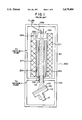
- FIG. 2 is a simplified cross-sectional diagram which illustrates a prior art rotating mandrel assembly with heat exchange.
- FIG. 3 is a cross-section of a model of a substrate and a cooling block separated by a gap.
- FIG. 4 shows graphs of thermal conductivity as a function of temperature for hydrogen, helium, oxygen, carbon dioxide, and air.
- FIG. 5 shows a cross-section of an arrangement of cooling block, substrate, and gas gap in accordance with an embodiment of the invention.
- FIGS. 6 and 7 show a further embodiment of the invention wherein a substrate holder is employed in spaced relation to the cooling block, and the cross-section of FIG. 6 is a section taken through a plane represented by the arrows 6--6 in FIG. 7.
- FIG. 8 is top view of a further embodiment of the invention.
- FIG. 9 is a cross-sectional partially broken away view which illustrates a further feature of the invention.
- FIG. 10 is a cross-sectional view of a further embodiment of the invention.
- FIG. 11 is a cross-sectional view of a further embodiment of the invention.
- FIGS. 12 and 13 show a further embodiment of the invention wherein a substrate holder is employed in space relation to a cooling block, and the cross-section of FIG. 12 is a section taken through a plane represented by the arrows 12--12 in FIG. 13.
- FIG. 14 is a cross-sectional view of a further feature wherein injected gas is utilized.
- FIG. 15 is a simplified diagram which shows the use of a robot arm in a deposition chamber.
- a deposition chamber 100 is the lower section of a plasma jet CVD deposition system 200, evacuated by one or more vacuum pumping systems (not shown).
- the system 200 is contained within a vacuum housing 211 and includes an arc-forming section 215 which comprises a cylindrical holder 294, a rod-like cathode 292, and an injector 295 mounted adjacent to the cathode so as to permit injected fluid to pass over the cathode.
- a cylindrical anode is provided at 291.
- the input fluid may be, for example, a mixture of hydrogen and methane. The methane could alternatively be fed in downstream.
- the anode 291 and cathode 292 are energized by a source of electrical power (not shown), for example a DC potential.
- Cylindrical magnets, designated by reference numeral 217 are utilized to help control the plasma generation.
- a nozzle, represented at 115, can be used to control beam size, within limitations.
- Optional cooling coils 234, in which a coolant can be circulated, can be located within the magnets.
- a mixture of hydrogen and methane is fed into the injector 295, and a plasma is obtained in front of the arc forming section and directed toward the deposition region at which a substrate is located.
- synthetic polycrystalline diamond can be formed from the described plasma, as the carbon in the methane is selectively deposited as diamond, and the graphite which forms is dissipated by combination with the hydrogen facilitating gas.
- suitable types of deposition equipment including, for example, other types of CVD deposition equipment, or physical vapor deposition equipment, can be used in conjunction with the features of the invention to be described.
- a mandrel 110 is rotatable on a shaft 111, and has a spacer 120 and a substrate 170 mounted thereon (by means not shown, bolting or clamping being typical).
- the mandrel 110 is a cooling block that can be cooled by any suitable means, for example by using a heat exchange fluid (e.g. water) that is circulated through the block or through another component in thermal contact with the block.
- a heat exchange fluid e.g. water
- FIG. 2 where a rotatable cooling block 110, coupled with a rotary union 115, is rotated, such as by a belt or gear drive (not shown), and coolant fluid can be circulated through the cooling block, in the direction indicated by the arrows, or in the opposite direction.
- the cooling block can be tilted with respect to the direction of the plasma jet, as disclosed in U.S. Pat. No. 5,342,660, and a suitable motor (not shown) can be used for rotating the shaft, as is also disclosed in U.S. Pat. No. 5,342,660.
- the rotational drive will conventionally be above the rotary union.
- the disclosed embodiments hereof can operate on a cooling block which is rotatable, as shown, or which is stationary.
- FIG. 3 shows a substrate 310 having its bottom surface 310B spaced from the top surface 320T of the cooling block 320 by a hydrogen gas containing gap 350.
- the conduction across the gap can be modeled by the one dimensional heat transfer equation
- Equation (1) indicates that the heat flow proceeds by conduction, rather than radiation or convention. Assuming that temperature varies approximately linearly across the gap, equation (1) can be written as
- Equation (2) can be used to compute the gap width that will handle the heat flux at the specified operating temperature differential.
- FIG. 4 shows the thermal conductivity of hydrogen helium, oxygen, carbon dioxide, and air as a function of temperature. The curve values are approximately applicable over a range of operating pressures between 0.05 atmospheres and 10 atmospheres. Assume that for one example of CVD arc jet plasma deposition the substrate back surface temperature is 700 degrees C. and the cooling block surface temperature is 100 degrees C.
- the average temperature in the gap is about 400 degrees C. and, at this temperature, FIG. 4 shows that the thermal conductivity of hydrogen is about 0.0033 Watts/cm-°C. If the heat flux from the plasma beam is approximately 30 Watts/cm 2 , the required gap dimension can be computed from equation (2) as:
- the CVD arc jet plasma deposition operates with a heat flux of 50 Watts/cm 2 , a substrate back surface temperature at 1000 degrees C., and a cooling block surface temperature of 125 degrees C.
- the average temperature in the gap is about 560 degrees and, at this temperature, FIG. 4 shows that the thermal conductivity of hydrogen is about 0.0039 Watts/cm-°C. so we have from equation (2):
- a hydrogen containing gap of about 0.07 cm is suitable for the conditions of these examples.
- a gap range of 0.01 cm to 0.30 cm is preferred in covering a range of operating conditions with at least 30 percent hydrogen in the gas gap. If the gap is too small, there can be difficulty in maintaining the correct standoff over the entire substrate area.
- the gas in the gap will be substantially the same as the gas environment in the deposition chamber although a gas may be injected into and/or confined in the gap.
- the cooling block 520 has a two-tiered annular shoulder 521 for supporting a disc-shaped substrate 510 above the cooling block top surface 525.
- the substrate can be any suitable material, for example, silicon.
- the structure 521 can be integral with the cooling block, or a separate unit as in some of the embodiments below.
- the cooling block 520 and its two-tiered annular support is similar to that of FIG. 5.
- a disc-shaped substrate holder 610 is utilized.
- the substrate holder can be formed of any suitable material, for example, molybdenum.
- the substrate holder can hold substrates of any desired shape.
- the substrate holder has recesses that receive and hold cutting tool inserts 611, which are shown in a top view in FIG. 7. Operation is similar to that previously described, with the gas gap providing the desired heat conduction path between the substrate holder and the cooling block at the desired operating temperatures to handle the heat flux into the substrates and substrate holder.
- a suitable substrate holder may be substituted for an illustrated substrate, or vice versa.
- FIG. 8 shows, in a top view, that only three small sections of the two-tiered annular ridge 521 of the FIG. 5 or FIG. 6 embodiment need be utilized to hold the substrate.
- the three annular ridge sections, 521A, 521B, and 521C act as a frame that contacts the substrate or substrate holder over less area, to minimize thermal conduction from the substrate to the cooling block through the solid structure.
- the shoulder of each ridge can be provided with a pin 528 and pad 529, formed, for example, of a thermally insulating material such as a ceramic.
- the length of the pins 528 which are seated in receiving holes, can be used to adjust the gap standoff.
- the ridge for supporting the substrate or substrate holder is shown as part of the cooling block.
- the ridge or frame can be a separate piece or pieces.
- the ridge (or ridge sections) is on a ring 1021 that fits on the matching surface of cylindrical cooling block 1020.
- the ring or frame can be a two piece construction that holds and secures the substrate with screws 1140. The frame again fits on the cooling block 1020, as shown.
- FIGS. 12 and 13 illustrate a further embodiment wherein the cooling block 1220 has three holes equidistant from the center thereof which receive respective pins 1201, 1202 and 1203.
- the distance of each pin from the center of the cylindrical cooling block corresponds to the radius of an annular groove 1214 in the bottom of a substrate holder 1210, so that when the substrate holder is placed over the cooling block, the pins engage the groove and define the offset of gap 1250.
- Different pin sizes can be used to obtain different gaps, and the pins can be formed of an insulating material to minimize thermal conduction through the pins.
- the annular rim shown at 1211 facilitates gripping of the substrate holder with a mechanical arm. If necessary or desirable, the substrate holder can be bolted or clamped in place by means not shown.
- the cooling block 1420 (or an attachment thereto, which is considered part of the cooling block for purposes hereof) can include inlet passages such as 1431 and 1432, and outlet passages 1435.
- a substrate or substrate holder 1410 is mounted as before.
- a gas can be injected into the inlet passages 1431 and 1432 and exhausted through the outlet passages 1435.
- a first gas such as hydrogen
- argon which has a much lower conductivity than hydrogen
- passages 1432 can be injected in a controlled manner into passages 1432 to control thermal conductivity of the gap 1410 as a function of radial position.
- a spatial variation of the gap thermal conductivity may also be established by varying the thickness of the gap as a function of radial position.
- FIG. 15 generally represents a CVD plasma deposition chamber 1560 which may be of the type previously described, and which employs the gas gap feature hereof.
- the deposition chamber also includes a mechanical arm 1565 (sometimes called a robot arm) that can be controlled from outside the deposition chamber manually, automatically, or semi-automatically, to change substrates or substrate holders without the need for opening the chamber, so that appropriate pressure conditions need not be reestablished from scratch each time a new substrate is put in place.
- a mechanical arm 1565 sometimes called a robot arm
- the chamber can be initially provided with a supply of substrates or substrate holders (represented at 1510A) and, after deposition on a substrate (or substrates in a substrate holder) on the cooling block 1220, the robot arm 1565 can be operated to remove the substrate (or substrate holder) from the cooling block 1220, place it aside in the chamber (e.g. at 1510B), take another substrate (or substrate holder with substrates in place), and place it on the cooling block 1220. Deposition can then be implemented, and the substrate moving procedure repeated. If desired, each substrate in the supply can be pre-mounted in a ring structure as in FIG. 11, so that the robot arm will handle the ring structure rather than the substrate itself.
- the robot arm 1565 can be of known type, which is articulated with an elbow 1566 and wrist 1567, and which engages and releases workpieces with a fork 1568.
- the robot arm, the supply of substrates, and/or other items can be in one or more auxiliary chambers, which can be considered as part of the main chamber for purposes hereof.
- a so-called "load lock" and/or any suitable valving arrangement can be used, as is known in the robotics art.
Landscapes
- Chemical & Material Sciences (AREA)
- General Chemical & Material Sciences (AREA)
- Chemical Kinetics & Catalysis (AREA)
- Engineering & Computer Science (AREA)
- Materials Engineering (AREA)
- Mechanical Engineering (AREA)
- Metallurgy (AREA)
- Organic Chemistry (AREA)
- Chemical Vapour Deposition (AREA)
- Crystals, And After-Treatments Of Crystals (AREA)
Priority Applications (6)
| Application Number | Priority Date | Filing Date | Title |
|---|---|---|---|
| US08/480,580 US5679404A (en) | 1995-06-07 | 1995-06-07 | Method for depositing a substance with temperature control |
| CA002177645A CA2177645C (en) | 1995-06-07 | 1996-05-29 | Apparatus and method for depositing a substance with temperature control |
| DE69629980T DE69629980T2 (de) | 1995-06-07 | 1996-05-29 | Methode mit Temperaturreglung zum Abscheiden eines Werkstoffes |
| EP96201480A EP0747505B1 (de) | 1995-06-07 | 1996-05-29 | Methode mit Temperaturreglung zum Abscheiden eines Werkstoffes |
| JP8146131A JPH0925195A (ja) | 1995-06-07 | 1996-06-07 | 物質堆積方法及び装置 |
| US08/863,763 US6099652A (en) | 1995-06-07 | 1997-05-27 | Apparatus and method for depositing a substance with temperature control |
Applications Claiming Priority (1)
| Application Number | Priority Date | Filing Date | Title |
|---|---|---|---|
| US08/480,580 US5679404A (en) | 1995-06-07 | 1995-06-07 | Method for depositing a substance with temperature control |
Related Child Applications (1)
| Application Number | Title | Priority Date | Filing Date |
|---|---|---|---|
| US08/863,763 Division US6099652A (en) | 1995-06-07 | 1997-05-27 | Apparatus and method for depositing a substance with temperature control |
Publications (1)
| Publication Number | Publication Date |
|---|---|
| US5679404A true US5679404A (en) | 1997-10-21 |
Family
ID=23908514
Family Applications (2)
| Application Number | Title | Priority Date | Filing Date |
|---|---|---|---|
| US08/480,580 Expired - Fee Related US5679404A (en) | 1995-06-07 | 1995-06-07 | Method for depositing a substance with temperature control |
| US08/863,763 Expired - Fee Related US6099652A (en) | 1995-06-07 | 1997-05-27 | Apparatus and method for depositing a substance with temperature control |
Family Applications After (1)
| Application Number | Title | Priority Date | Filing Date |
|---|---|---|---|
| US08/863,763 Expired - Fee Related US6099652A (en) | 1995-06-07 | 1997-05-27 | Apparatus and method for depositing a substance with temperature control |
Country Status (5)
| Country | Link |
|---|---|
| US (2) | US5679404A (de) |
| EP (1) | EP0747505B1 (de) |
| JP (1) | JPH0925195A (de) |
| CA (1) | CA2177645C (de) |
| DE (1) | DE69629980T2 (de) |
Cited By (15)
| Publication number | Priority date | Publication date | Assignee | Title |
|---|---|---|---|---|
| US6099652A (en) * | 1995-06-07 | 2000-08-08 | Saint-Gobain Industrial Ceramics, Inc. | Apparatus and method for depositing a substance with temperature control |
| US6294025B1 (en) * | 1996-11-01 | 2001-09-25 | THEVA DüNNSCHICHTTECHNIK GMBH | Device for producing oxidic thin films |
| US6318957B1 (en) * | 1998-07-10 | 2001-11-20 | Asm America, Inc. | Method for handling of wafers with minimal contact |
| US6423597B1 (en) * | 2000-11-09 | 2002-07-23 | United Microelectronics Corp. | Structure of a DRAM and a manufacturing process thereof |
| US20030194881A1 (en) * | 2002-04-15 | 2003-10-16 | Mitsubishi Denki Kabushiki Kaisha | Process for manufacturing a semiconductor device |
| US20050011768A1 (en) * | 1997-12-31 | 2005-01-20 | Stone William M. | Workpiece chuck |
| US6935618B2 (en) | 2002-12-18 | 2005-08-30 | Masco Corporation Of Indiana | Valve component with multiple surface layers |
| US20060225720A1 (en) * | 1998-07-31 | 2006-10-12 | Norton Company | Rotary dressing tool containing brazed diamond layer |
| US7866343B2 (en) | 2002-12-18 | 2011-01-11 | Masco Corporation Of Indiana | Faucet |
| US7866342B2 (en) | 2002-12-18 | 2011-01-11 | Vapor Technologies, Inc. | Valve component for faucet |
| US8123967B2 (en) | 2005-08-01 | 2012-02-28 | Vapor Technologies Inc. | Method of producing an article having patterned decorative coating |
| US8220489B2 (en) | 2002-12-18 | 2012-07-17 | Vapor Technologies Inc. | Faucet with wear-resistant valve component |
| US8555921B2 (en) | 2002-12-18 | 2013-10-15 | Vapor Technologies Inc. | Faucet component with coating |
| EP2656370A2 (de) | 2010-12-23 | 2013-10-30 | Element Six Limited | Mikrowellenplasmareaktoren und substrate für die herstellung synthetischer diamanten |
| CN114334612A (zh) * | 2022-03-14 | 2022-04-12 | 广州粤芯半导体技术有限公司 | 半导体器件及其制造方法 |
Families Citing this family (19)
| Publication number | Priority date | Publication date | Assignee | Title |
|---|---|---|---|---|
| DE19718618C2 (de) | 1997-05-02 | 1999-12-02 | Daimler Chrysler Ag | Komposit-Struktur mit einem mehrere mikroelektronische Bauteile und eine Diamantschicht aufweisenden Wachstums-Substrat sowie Verfahren zur Herstellung der Komposit-Struktur |
| DE19718518C2 (de) * | 1997-05-02 | 1999-11-04 | Daimler Chrysler Ag | Verfahren und Vorrichtung zur Abscheidung von Diamant auf einem Substrat und Verwendung |
| JP4260307B2 (ja) * | 1999-09-28 | 2009-04-30 | 芝浦メカトロニクス株式会社 | 気相成長装置 |
| US20060222756A1 (en) * | 2000-09-29 | 2006-10-05 | Cordis Corporation | Medical devices, drug coatings and methods of maintaining the drug coatings thereon |
| AU9486901A (en) | 2000-09-29 | 2002-04-08 | Cordis Corp | Coated medical devices |
| DE10052724B4 (de) * | 2000-10-24 | 2012-08-02 | Pac Tech-Packaging Technologies Gmbh | Behandlungseinrichtung für Wafer |
| TWI272689B (en) | 2001-02-16 | 2007-02-01 | Tokyo Electron Ltd | Method and apparatus for transferring heat from a substrate to a chuck |
| DE10149588B4 (de) * | 2001-10-08 | 2017-09-07 | Oerlikon Trading Ag, Trübbach | Verfahren zur Diamantbeschichtung von Substraten |
| JP3908112B2 (ja) * | 2002-07-29 | 2007-04-25 | Sumco Techxiv株式会社 | サセプタ、エピタキシャルウェーハ製造装置及びエピタキシャルウェーハ製造方法 |
| US7491234B2 (en) * | 2002-12-03 | 2009-02-17 | Boston Scientific Scimed, Inc. | Medical devices for delivery of therapeutic agents |
| US20040206304A1 (en) * | 2003-04-15 | 2004-10-21 | Menear John Edgar | Pressurized chuck for controlling backside wafer contamination |
| US9498563B2 (en) * | 2004-04-23 | 2016-11-22 | Boston Scientific Scimed, Inc. | Medical articles having therapeutic-agent-containing regions formed from coalesced polymer particles |
| GB0509499D0 (en) * | 2005-05-11 | 2005-06-15 | Univ Surrey | Use of thermal barrier for low temperature growth of nanostructures using top-down heating approach |
| DE102006018514A1 (de) * | 2006-04-21 | 2007-10-25 | Aixtron Ag | Vorrichtung und Verfahren zur Steuerung der Oberflächentemperatur eines Substrates in einer Prozesskammer |
| CN102651331A (zh) * | 2011-06-14 | 2012-08-29 | 京东方科技集团股份有限公司 | 基板托盘及柔性电子器件制造方法 |
| US20140293291A1 (en) * | 2013-04-01 | 2014-10-02 | Kla-Tencor Corporation | Wafer Shape and Thickness Measurement System Utilizing Shearing Interferometers |
| DE102014104218A1 (de) * | 2014-03-26 | 2015-10-01 | Aixtron Se | CVD-Reaktor mit Vorlaufzonen-Temperaturregelung |
| CN215757604U (zh) * | 2021-01-25 | 2022-02-08 | 苏州晶湛半导体有限公司 | 石墨盘 |
| DE102024130537A1 (de) * | 2024-10-21 | 2026-04-23 | Condias Gmbh | Mit Diamant beschichtetes AIN-Substrat und Verfahren zum Herstellen |
Citations (36)
| Publication number | Priority date | Publication date | Assignee | Title |
|---|---|---|---|---|
| US3845739A (en) * | 1972-04-17 | 1974-11-05 | Xerox Corp | System for vapor deposition of thin films |
| US4401054A (en) * | 1980-05-02 | 1983-08-30 | Nippon Telegraph & Telephone Public Corporation | Plasma deposition apparatus |
| JPS5921026A (ja) * | 1982-07-28 | 1984-02-02 | Hitachi Ltd | 半導体製造装置 |
| JPS5943861A (ja) * | 1982-09-03 | 1984-03-12 | Ulvac Corp | ル−バ−式化学的蒸着装置 |
| US4471003A (en) * | 1980-11-25 | 1984-09-11 | Cann Gordon L | Magnetoplasmadynamic apparatus and process for the separation and deposition of materials |
| US4487162A (en) * | 1980-11-25 | 1984-12-11 | Cann Gordon L | Magnetoplasmadynamic apparatus for the separation and deposition of materials |
| US4505947A (en) * | 1982-07-14 | 1985-03-19 | The Standard Oil Company (Ohio) | Method for the deposition of coatings upon substrates utilizing a high pressure, non-local thermal equilibrium arc plasma |
| US4507588A (en) * | 1983-02-28 | 1985-03-26 | Board Of Trustees Operating Michigan State University | Ion generating apparatus and method for the use thereof |
| US4585668A (en) * | 1983-02-28 | 1986-04-29 | Michigan State University | Method for treating a surface with a microwave or UHF plasma and improved apparatus |
| US4596718A (en) * | 1984-06-19 | 1986-06-24 | Plasmainvent Ag | Vacuum plasma coating apparatus |
| US4630566A (en) * | 1984-08-16 | 1986-12-23 | Board Of Trustees Operating Michigan State University | Microwave or UHF plasma improved apparatus |
| US4691662A (en) * | 1983-02-28 | 1987-09-08 | Michigan State University | Dual plasma microwave apparatus and method for treating a surface |
| US4728863A (en) * | 1985-12-04 | 1988-03-01 | Wertheimer Michael R | Apparatus and method for plasma treatment of substrates |
| JPS63289926A (ja) * | 1987-05-22 | 1988-11-28 | Canon Inc | 堆積膜形成装置及びプラズマ処理装置 |
| JPH01242141A (ja) * | 1988-03-23 | 1989-09-27 | Hitachi Ltd | 高気圧マイクロ波プラズマ反応装置 |
| JPH01312008A (ja) * | 1988-06-11 | 1989-12-15 | Nkk Corp | 金属間化合物合金材の製造方法 |
| JPH0260103A (ja) * | 1988-08-26 | 1990-02-28 | Uchiya Thermostat Kk | 溶射技術を用いた抵抗体の製造方法 |
| US4913090A (en) * | 1987-10-02 | 1990-04-03 | Mitsubishi Denki Kabushiki Kaisha | Chemical vapor deposition apparatus having cooling heads adjacent to gas dispersing heads in a single chamber |
| JPH02167891A (ja) * | 1988-12-20 | 1990-06-28 | Citizen Watch Co Ltd | ダイヤモンド膜気相合成装置 |
| US4979466A (en) * | 1986-12-01 | 1990-12-25 | Hitachi, Ltd. | Apparatus for selective deposition of metal thin film |
| US4987002A (en) * | 1988-05-09 | 1991-01-22 | Kabushiki Kaisha Kenwood | Process for forming a crystalline diamond film |
| US5063031A (en) * | 1989-08-24 | 1991-11-05 | Kabushiki Kaisha Toshiba | Apparatus for growing vapor phase layer on semiconductor substrate |
| US5068871A (en) * | 1989-08-04 | 1991-11-26 | Kabushiki Kaisha Toyota Chuo Kenkyusho | Process for synthesizing diamond and apparatus therefor |
| US5094878A (en) * | 1989-06-21 | 1992-03-10 | Nippon Soken, Inc. | Process for forming diamond film |
| US5104634A (en) * | 1989-04-20 | 1992-04-14 | Hercules Incorporated | Process for forming diamond coating using a silent discharge plasma jet process |
| US5108779A (en) * | 1988-05-26 | 1992-04-28 | General Electric Company | Diamond crystal growth process |
| US5132105A (en) * | 1990-02-02 | 1992-07-21 | Quantametrics, Inc. | Materials with diamond-like properties and method and means for manufacturing them |
| US5204145A (en) * | 1991-03-04 | 1993-04-20 | General Electric Company | Apparatus for producing diamonds by chemical vapor deposition and articles produced therefrom |
| US5204144A (en) * | 1991-05-10 | 1993-04-20 | Celestech, Inc. | Method for plasma deposition on apertured substrates |
| US5226383A (en) * | 1992-03-12 | 1993-07-13 | Bell Communications Research, Inc. | Gas foil rotating substrate holder |
| US5314570A (en) * | 1990-07-18 | 1994-05-24 | Sumitomo Electric Industries Ltd. | Process and apparatus for the production of diamond |
| US5318801A (en) * | 1993-05-18 | 1994-06-07 | United States Of America As Represented By The Secretary Of The Navy | Substrate temperature control apparatus and technique for CVD reactors |
| US5340401A (en) * | 1989-01-06 | 1994-08-23 | Celestech Inc. | Diamond deposition cell |
| US5342660A (en) * | 1991-05-10 | 1994-08-30 | Celestech, Inc. | Method for plasma jet deposition |
| US5411076A (en) * | 1993-02-12 | 1995-05-02 | Dainippon Screen Mfg. Co., Ltd. Corp. Of Japan | Substrate cooling device and substrate heat-treating apparatus |
| US5567267A (en) * | 1992-11-20 | 1996-10-22 | Tokyo Electron Limited | Method of controlling temperature of susceptor |
Family Cites Families (17)
| Publication number | Priority date | Publication date | Assignee | Title |
|---|---|---|---|---|
| US4457259A (en) * | 1983-03-14 | 1984-07-03 | Rca Corporation | Apparatus for spraying a liquid on a spinning surface |
| US4527620A (en) * | 1984-05-02 | 1985-07-09 | Varian Associates, Inc. | Apparatus for controlling thermal transfer in a cyclic vacuum processing system |
| US4999320A (en) * | 1988-03-31 | 1991-03-12 | Texas Instruments Incorporated | Method for suppressing ionization avalanches in a helium wafer cooling assembly |
| US4949783A (en) * | 1988-05-18 | 1990-08-21 | Veeco Instruments, Inc. | Substrate transport and cooling apparatus and method for same |
| US5488774A (en) * | 1990-01-24 | 1996-02-06 | Janowski; Leonard J. | Cutting edges |
| KR940011708B1 (ko) * | 1990-04-09 | 1994-12-23 | 니찌덴 아네루바 가부시끼가이샤 | 기판온도제어기구 |
| KR0165898B1 (ko) * | 1990-07-02 | 1999-02-01 | 미다 가쓰시게 | 진공처리방법 및 장치 |
| US5221403A (en) * | 1990-07-20 | 1993-06-22 | Tokyo Electron Limited | Support table for plate-like body and processing apparatus using the table |
| ZA921208B (en) * | 1991-03-04 | 1993-02-24 | Gen Electric | Apparatus for producing diamonds by chemical vapor deposition and articles produced therefrom |
| US5803977A (en) * | 1992-09-30 | 1998-09-08 | Applied Materials, Inc. | Apparatus for full wafer deposition |
| DE4305750C2 (de) * | 1993-02-25 | 2002-03-21 | Unaxis Deutschland Holding | Vorrichtung zum Halten von flachen, kreisscheibenförmigen Substraten in der Vakuumkammer einer Beschichtungs- oder Ätzanlage |
| US5738165A (en) * | 1993-05-07 | 1998-04-14 | Nikon Corporation | Substrate holding apparatus |
| TW277139B (de) * | 1993-09-16 | 1996-06-01 | Hitachi Seisakusyo Kk | |
| US5595241A (en) * | 1994-10-07 | 1997-01-21 | Sony Corporation | Wafer heating chuck with dual zone backplane heating and segmented clamping member |
| EP0871843B1 (de) * | 1994-10-17 | 2003-05-14 | Varian Semiconductor Equipment Associates Inc. | Montageelement und methode zum klemmen eines flachen, dünnen und leitfähigen werkstückes |
| US5551983A (en) * | 1994-11-01 | 1996-09-03 | Celestech, Inc. | Method and apparatus for depositing a substance with temperature control |
| US5679404A (en) * | 1995-06-07 | 1997-10-21 | Saint-Gobain/Norton Industrial Ceramics Corporation | Method for depositing a substance with temperature control |
-
1995
- 1995-06-07 US US08/480,580 patent/US5679404A/en not_active Expired - Fee Related
-
1996
- 1996-05-29 CA CA002177645A patent/CA2177645C/en not_active Expired - Fee Related
- 1996-05-29 EP EP96201480A patent/EP0747505B1/de not_active Expired - Lifetime
- 1996-05-29 DE DE69629980T patent/DE69629980T2/de not_active Expired - Fee Related
- 1996-06-07 JP JP8146131A patent/JPH0925195A/ja active Pending
-
1997
- 1997-05-27 US US08/863,763 patent/US6099652A/en not_active Expired - Fee Related
Patent Citations (38)
| Publication number | Priority date | Publication date | Assignee | Title |
|---|---|---|---|---|
| US3845739A (en) * | 1972-04-17 | 1974-11-05 | Xerox Corp | System for vapor deposition of thin films |
| US4401054A (en) * | 1980-05-02 | 1983-08-30 | Nippon Telegraph & Telephone Public Corporation | Plasma deposition apparatus |
| US4471003A (en) * | 1980-11-25 | 1984-09-11 | Cann Gordon L | Magnetoplasmadynamic apparatus and process for the separation and deposition of materials |
| US4487162A (en) * | 1980-11-25 | 1984-12-11 | Cann Gordon L | Magnetoplasmadynamic apparatus for the separation and deposition of materials |
| US4505947A (en) * | 1982-07-14 | 1985-03-19 | The Standard Oil Company (Ohio) | Method for the deposition of coatings upon substrates utilizing a high pressure, non-local thermal equilibrium arc plasma |
| JPS5921026A (ja) * | 1982-07-28 | 1984-02-02 | Hitachi Ltd | 半導体製造装置 |
| JPS5943861A (ja) * | 1982-09-03 | 1984-03-12 | Ulvac Corp | ル−バ−式化学的蒸着装置 |
| US4585668A (en) * | 1983-02-28 | 1986-04-29 | Michigan State University | Method for treating a surface with a microwave or UHF plasma and improved apparatus |
| US4507588A (en) * | 1983-02-28 | 1985-03-26 | Board Of Trustees Operating Michigan State University | Ion generating apparatus and method for the use thereof |
| US4691662A (en) * | 1983-02-28 | 1987-09-08 | Michigan State University | Dual plasma microwave apparatus and method for treating a surface |
| US4596718A (en) * | 1984-06-19 | 1986-06-24 | Plasmainvent Ag | Vacuum plasma coating apparatus |
| US4596718B1 (de) * | 1984-06-19 | 1989-10-17 | ||
| US4630566A (en) * | 1984-08-16 | 1986-12-23 | Board Of Trustees Operating Michigan State University | Microwave or UHF plasma improved apparatus |
| US4728863A (en) * | 1985-12-04 | 1988-03-01 | Wertheimer Michael R | Apparatus and method for plasma treatment of substrates |
| US4979466A (en) * | 1986-12-01 | 1990-12-25 | Hitachi, Ltd. | Apparatus for selective deposition of metal thin film |
| JPS63289926A (ja) * | 1987-05-22 | 1988-11-28 | Canon Inc | 堆積膜形成装置及びプラズマ処理装置 |
| US4913090A (en) * | 1987-10-02 | 1990-04-03 | Mitsubishi Denki Kabushiki Kaisha | Chemical vapor deposition apparatus having cooling heads adjacent to gas dispersing heads in a single chamber |
| JPH01242141A (ja) * | 1988-03-23 | 1989-09-27 | Hitachi Ltd | 高気圧マイクロ波プラズマ反応装置 |
| US4987002A (en) * | 1988-05-09 | 1991-01-22 | Kabushiki Kaisha Kenwood | Process for forming a crystalline diamond film |
| US5108779A (en) * | 1988-05-26 | 1992-04-28 | General Electric Company | Diamond crystal growth process |
| JPH01312008A (ja) * | 1988-06-11 | 1989-12-15 | Nkk Corp | 金属間化合物合金材の製造方法 |
| JPH0260103A (ja) * | 1988-08-26 | 1990-02-28 | Uchiya Thermostat Kk | 溶射技術を用いた抵抗体の製造方法 |
| JPH02167891A (ja) * | 1988-12-20 | 1990-06-28 | Citizen Watch Co Ltd | ダイヤモンド膜気相合成装置 |
| US5340401A (en) * | 1989-01-06 | 1994-08-23 | Celestech Inc. | Diamond deposition cell |
| US5104634A (en) * | 1989-04-20 | 1992-04-14 | Hercules Incorporated | Process for forming diamond coating using a silent discharge plasma jet process |
| US5094878A (en) * | 1989-06-21 | 1992-03-10 | Nippon Soken, Inc. | Process for forming diamond film |
| US5068871A (en) * | 1989-08-04 | 1991-11-26 | Kabushiki Kaisha Toyota Chuo Kenkyusho | Process for synthesizing diamond and apparatus therefor |
| US5063031A (en) * | 1989-08-24 | 1991-11-05 | Kabushiki Kaisha Toshiba | Apparatus for growing vapor phase layer on semiconductor substrate |
| US5132105A (en) * | 1990-02-02 | 1992-07-21 | Quantametrics, Inc. | Materials with diamond-like properties and method and means for manufacturing them |
| US5314570A (en) * | 1990-07-18 | 1994-05-24 | Sumitomo Electric Industries Ltd. | Process and apparatus for the production of diamond |
| US5204145A (en) * | 1991-03-04 | 1993-04-20 | General Electric Company | Apparatus for producing diamonds by chemical vapor deposition and articles produced therefrom |
| US5204144A (en) * | 1991-05-10 | 1993-04-20 | Celestech, Inc. | Method for plasma deposition on apertured substrates |
| US5342660A (en) * | 1991-05-10 | 1994-08-30 | Celestech, Inc. | Method for plasma jet deposition |
| US5226383A (en) * | 1992-03-12 | 1993-07-13 | Bell Communications Research, Inc. | Gas foil rotating substrate holder |
| US5567267A (en) * | 1992-11-20 | 1996-10-22 | Tokyo Electron Limited | Method of controlling temperature of susceptor |
| US5411076A (en) * | 1993-02-12 | 1995-05-02 | Dainippon Screen Mfg. Co., Ltd. Corp. Of Japan | Substrate cooling device and substrate heat-treating apparatus |
| US5318801A (en) * | 1993-05-18 | 1994-06-07 | United States Of America As Represented By The Secretary Of The Navy | Substrate temperature control apparatus and technique for CVD reactors |
| US5527392A (en) * | 1993-05-18 | 1996-06-18 | The United States Of America As Represented By The Secretary Of The Navy | Substrate temperature control apparatus for CVD reactors |
Cited By (25)
| Publication number | Priority date | Publication date | Assignee | Title |
|---|---|---|---|---|
| US6099652A (en) * | 1995-06-07 | 2000-08-08 | Saint-Gobain Industrial Ceramics, Inc. | Apparatus and method for depositing a substance with temperature control |
| US6294025B1 (en) * | 1996-11-01 | 2001-09-25 | THEVA DüNNSCHICHTTECHNIK GMBH | Device for producing oxidic thin films |
| US20050011768A1 (en) * | 1997-12-31 | 2005-01-20 | Stone William M. | Workpiece chuck |
| US7331097B2 (en) | 1997-12-31 | 2008-02-19 | Temptronic Corporation | Method of manufacturing a workpiece chuck |
| US6318957B1 (en) * | 1998-07-10 | 2001-11-20 | Asm America, Inc. | Method for handling of wafers with minimal contact |
| US8579681B2 (en) | 1998-07-31 | 2013-11-12 | Saint-Gobain Abrasives, Inc. | Rotary dressing tool containing brazed diamond layer |
| US20060225720A1 (en) * | 1998-07-31 | 2006-10-12 | Norton Company | Rotary dressing tool containing brazed diamond layer |
| US8192256B2 (en) | 1998-07-31 | 2012-06-05 | Saint-Gobain Abrasives, Inc. | Rotary dressing tool containing brazed diamond layer |
| US6423597B1 (en) * | 2000-11-09 | 2002-07-23 | United Microelectronics Corp. | Structure of a DRAM and a manufacturing process thereof |
| US20030194881A1 (en) * | 2002-04-15 | 2003-10-16 | Mitsubishi Denki Kabushiki Kaisha | Process for manufacturing a semiconductor device |
| US6933250B2 (en) * | 2002-04-15 | 2005-08-23 | Mitsubishi Denki Kabushiki Kaisha | Process for manufacturing a semiconductor device |
| US7866343B2 (en) | 2002-12-18 | 2011-01-11 | Masco Corporation Of Indiana | Faucet |
| US9388910B2 (en) | 2002-12-18 | 2016-07-12 | Delta Faucet Company | Faucet component with coating |
| US7866342B2 (en) | 2002-12-18 | 2011-01-11 | Vapor Technologies, Inc. | Valve component for faucet |
| US8118055B2 (en) | 2002-12-18 | 2012-02-21 | Vapor Technologies Inc. | Valve component for faucet |
| US9909677B2 (en) | 2002-12-18 | 2018-03-06 | Delta Faucet Company | Faucet component with coating |
| US7216661B2 (en) | 2002-12-18 | 2007-05-15 | Masco Corporation Of Indiana | Method of forming a wear resistant component |
| US8220489B2 (en) | 2002-12-18 | 2012-07-17 | Vapor Technologies Inc. | Faucet with wear-resistant valve component |
| US8555921B2 (en) | 2002-12-18 | 2013-10-15 | Vapor Technologies Inc. | Faucet component with coating |
| US7445026B2 (en) | 2002-12-18 | 2008-11-04 | Masco Corporation Of Indiana | Valve component with improved wear resistance |
| US6935618B2 (en) | 2002-12-18 | 2005-08-30 | Masco Corporation Of Indiana | Valve component with multiple surface layers |
| US8123967B2 (en) | 2005-08-01 | 2012-02-28 | Vapor Technologies Inc. | Method of producing an article having patterned decorative coating |
| EP2656370A2 (de) | 2010-12-23 | 2013-10-30 | Element Six Limited | Mikrowellenplasmareaktoren und substrate für die herstellung synthetischer diamanten |
| CN114334612A (zh) * | 2022-03-14 | 2022-04-12 | 广州粤芯半导体技术有限公司 | 半导体器件及其制造方法 |
| CN114334612B (zh) * | 2022-03-14 | 2022-06-28 | 广州粤芯半导体技术有限公司 | 半导体器件及其制造方法 |
Also Published As
| Publication number | Publication date |
|---|---|
| EP0747505A2 (de) | 1996-12-11 |
| EP0747505B1 (de) | 2003-09-17 |
| US6099652A (en) | 2000-08-08 |
| CA2177645A1 (en) | 1996-12-08 |
| CA2177645C (en) | 2000-10-03 |
| DE69629980T2 (de) | 2004-07-29 |
| EP0747505A3 (de) | 1998-03-11 |
| JPH0925195A (ja) | 1997-01-28 |
| DE69629980D1 (de) | 2003-10-23 |
Similar Documents
| Publication | Publication Date | Title |
|---|---|---|
| US6099652A (en) | Apparatus and method for depositing a substance with temperature control | |
| US5683759A (en) | Method for depositing a substance with temperature control | |
| KR102667399B1 (ko) | 극저온 냉각식 회전가능 정전 척 | |
| US5342660A (en) | Method for plasma jet deposition | |
| US5383971A (en) | Differential pressure CVD chuck | |
| US5403399A (en) | Method and apparatus for vapor deposition of diamond | |
| JP4531914B2 (ja) | 処理チャンバ内でウェハを支持する装置 | |
| US5935338A (en) | Chemical vapor deposition chamber | |
| US5534072A (en) | Integrated module multi-chamber CVD processing system and its method for processing subtrates | |
| EP0467390B1 (de) | Auflageplatte für plattenförmigen Körper sowie Behandlungsverfahren mit Verbrauch der Auflageplatte | |
| US20040226515A1 (en) | Heat transfer assembly | |
| KR20100016083A (ko) | 반도체 재료 프로세싱 장치용 저-입자 성능을 갖는 샤워헤드 전극 및 샤워헤드 전극 어셈블리 | |
| US20100151680A1 (en) | Substrate carrier with enhanced temperature uniformity | |
| US4651674A (en) | Apparatus for vapor deposition | |
| JP3714248B2 (ja) | 処理装置及び処理方法 | |
| JP4471848B2 (ja) | 基板保持装置 | |
| JPH0878338A (ja) | 半導体の製造装置 | |
| EP0583374B1 (de) | Verfahren und vorrichtung zur plasmabeschichtung | |
| EP0502657B1 (de) | Verbessertes Gerät zur Herstellung von Diamanten mittels chemischer Abscheidung aus der Dampfphase und damit hergestellter Gegenstand | |
| JP3865841B2 (ja) | 電子ビーム蒸着装置 | |
| JPH0857753A (ja) | ダイヤモンドの加工方法および加工装置 | |
| JP3081669B2 (ja) | 処理装置 | |
| CA2204164A1 (en) | Method and apparatus for depositing a substance with temperature control | |
| WO1996013623A1 (en) | Method and apparatus for depositing a substance with temperature control | |
| WO2025155610A1 (en) | Heat tuner for heating substrates in a processing tool |
Legal Events
| Date | Code | Title | Description |
|---|---|---|---|
| AS | Assignment |
Owner name: SAINT-GOBAIN/NORTON INDUSTRIAL CERAMICS CORPORATIO Free format text: ASSIGNMENT OF ASSIGNORS INTEREST;ASSIGNORS:PATTEN, DONALD O., JR.;SIMPSON, MATTHEW A.;WINDISCHMANN, HENRY;AND OTHERS;REEL/FRAME:007655/0627;SIGNING DATES FROM 19950816 TO 19950920 |
|
| AS | Assignment |
Owner name: WILLIAM A. QUIRK, CALIFORNIA Free format text: ASSIGNMENT OF ASSIGNORS INTEREST;ASSIGNOR:SAINT-GOBAIN/NORTON INDUSTRIAL CERAMICS CORPORATION;REEL/FRAME:008471/0997 Effective date: 19970414 Owner name: MICHAEL S. HEUSER, CALIFORNIA Free format text: ASSIGNMENT OF ASSIGNORS INTEREST;ASSIGNOR:SAINT-GOBAIN/NORTON INDUSTRIAL CERAMICS CORPORATION;REEL/FRAME:008471/0997 Effective date: 19970414 Owner name: CELESTECH, INC., CALIFORNIA Free format text: ASSIGNMENT OF ASSIGNORS INTEREST;ASSIGNORS:HEUSER, MICHAEL S.;QUIRK, WILLIAM A.;REEL/FRAME:008469/0928;SIGNING DATES FROM 19970324 TO 19970331 |
|
| FEPP | Fee payment procedure |
Free format text: PAYOR NUMBER ASSIGNED (ORIGINAL EVENT CODE: ASPN); ENTITY STATUS OF PATENT OWNER: LARGE ENTITY |
|
| FPAY | Fee payment |
Year of fee payment: 4 |
|
| REMI | Maintenance fee reminder mailed | ||
| LAPS | Lapse for failure to pay maintenance fees | ||
| STCH | Information on status: patent discontinuation |
Free format text: PATENT EXPIRED DUE TO NONPAYMENT OF MAINTENANCE FEES UNDER 37 CFR 1.362 |
|
| FP | Lapsed due to failure to pay maintenance fee |
Effective date: 20051021 |