US11024535B2 - Method for filling recessed features in semiconductor devices with a low-resistivity metal - Google Patents
Method for filling recessed features in semiconductor devices with a low-resistivity metal Download PDFInfo
- Publication number
- US11024535B2 US11024535B2 US16/598,772 US201916598772A US11024535B2 US 11024535 B2 US11024535 B2 US 11024535B2 US 201916598772 A US201916598772 A US 201916598772A US 11024535 B2 US11024535 B2 US 11024535B2
- Authority
- US
- United States
- Prior art keywords
- layer
- metal
- recessed feature
- patterned substrate
- recessed
- Prior art date
- Legal status (The legal status is an assumption and is not a legal conclusion. Google has not performed a legal analysis and makes no representation as to the accuracy of the status listed.)
- Active
Links
Images


Classifications
-
- H—ELECTRICITY
- H10—SEMICONDUCTOR DEVICES; ELECTRIC SOLID-STATE DEVICES NOT OTHERWISE PROVIDED FOR
- H10P—GENERIC PROCESSES OR APPARATUS FOR THE MANUFACTURE OR TREATMENT OF DEVICES COVERED BY CLASS H10
- H10P14/00—Formation of materials, e.g. in the shape of layers or pillars
- H10P14/40—Formation of materials, e.g. in the shape of layers or pillars of conductive or resistive materials
- H10P14/42—Formation of materials, e.g. in the shape of layers or pillars of conductive or resistive materials using a gas or vapour
- H10P14/43—Chemical deposition, e.g. chemical vapour deposition [CVD]
-
- H—ELECTRICITY
- H10—SEMICONDUCTOR DEVICES; ELECTRIC SOLID-STATE DEVICES NOT OTHERWISE PROVIDED FOR
- H10W—GENERIC PACKAGES, INTERCONNECTIONS, CONNECTORS OR OTHER CONSTRUCTIONAL DETAILS OF DEVICES COVERED BY CLASS H10
- H10W20/00—Interconnections in chips, wafers or substrates
- H10W20/01—Manufacture or treatment
- H10W20/071—Manufacture or treatment of dielectric parts thereof
- H10W20/074—Manufacture or treatment of dielectric parts thereof of dielectric parts comprising thin functional dielectric layers, e.g. dielectric etch-stop, barrier, capping or liner layers
- H10W20/077—Manufacture or treatment of dielectric parts thereof of dielectric parts comprising thin functional dielectric layers, e.g. dielectric etch-stop, barrier, capping or liner layers on sidewalls or on top surfaces of conductors
-
- H01L21/76826—
-
- H01L21/76831—
-
- H01L21/76844—
-
- H01L21/76868—
-
- H01L21/76879—
-
- H01L21/76888—
-
- H—ELECTRICITY
- H10—SEMICONDUCTOR DEVICES; ELECTRIC SOLID-STATE DEVICES NOT OTHERWISE PROVIDED FOR
- H10P—GENERIC PROCESSES OR APPARATUS FOR THE MANUFACTURE OR TREATMENT OF DEVICES COVERED BY CLASS H10
- H10P14/00—Formation of materials, e.g. in the shape of layers or pillars
- H10P14/20—Formation of materials, e.g. in the shape of layers or pillars of semiconductor materials
- H10P14/27—Formation of materials, e.g. in the shape of layers or pillars of semiconductor materials using selective deposition, e.g. simultaneous growth of monocrystalline and non-monocrystalline semiconductor materials
- H10P14/271—Formation of materials, e.g. in the shape of layers or pillars of semiconductor materials using selective deposition, e.g. simultaneous growth of monocrystalline and non-monocrystalline semiconductor materials characterised by the preparation of substrate for selective deposition
-
- H—ELECTRICITY
- H10—SEMICONDUCTOR DEVICES; ELECTRIC SOLID-STATE DEVICES NOT OTHERWISE PROVIDED FOR
- H10P—GENERIC PROCESSES OR APPARATUS FOR THE MANUFACTURE OR TREATMENT OF DEVICES COVERED BY CLASS H10
- H10P14/00—Formation of materials, e.g. in the shape of layers or pillars
- H10P14/20—Formation of materials, e.g. in the shape of layers or pillars of semiconductor materials
- H10P14/36—Formation of materials, e.g. in the shape of layers or pillars of semiconductor materials characterised by treatments done before the formation of the materials
-
- H—ELECTRICITY
- H10—SEMICONDUCTOR DEVICES; ELECTRIC SOLID-STATE DEVICES NOT OTHERWISE PROVIDED FOR
- H10P—GENERIC PROCESSES OR APPARATUS FOR THE MANUFACTURE OR TREATMENT OF DEVICES COVERED BY CLASS H10
- H10P14/00—Formation of materials, e.g. in the shape of layers or pillars
- H10P14/60—Formation of materials, e.g. in the shape of layers or pillars of insulating materials
- H10P14/66—Formation of materials, e.g. in the shape of layers or pillars of insulating materials characterised by the type of materials
- H10P14/668—Formation of materials, e.g. in the shape of layers or pillars of insulating materials characterised by the type of materials the materials being characterised by the deposition precursor materials
- H10P14/6681—Formation of materials, e.g. in the shape of layers or pillars of insulating materials characterised by the type of materials the materials being characterised by the deposition precursor materials the precursor containing a compound comprising Si
- H10P14/6682—Formation of materials, e.g. in the shape of layers or pillars of insulating materials characterised by the type of materials the materials being characterised by the deposition precursor materials the precursor containing a compound comprising Si the compound being a silane, e.g. disilane, methylsilane or chlorosilane
-
- H—ELECTRICITY
- H10—SEMICONDUCTOR DEVICES; ELECTRIC SOLID-STATE DEVICES NOT OTHERWISE PROVIDED FOR
- H10W—GENERIC PACKAGES, INTERCONNECTIONS, CONNECTORS OR OTHER CONSTRUCTIONAL DETAILS OF DEVICES COVERED BY CLASS H10
- H10W20/00—Interconnections in chips, wafers or substrates
- H10W20/01—Manufacture or treatment
- H10W20/031—Manufacture or treatment of conductive parts of the interconnections
- H10W20/032—Manufacture or treatment of conductive parts of the interconnections of conductive barrier, adhesion or liner layers
- H10W20/033—Manufacture or treatment of conductive parts of the interconnections of conductive barrier, adhesion or liner layers in openings in dielectrics
- H10W20/034—Manufacture or treatment of conductive parts of the interconnections of conductive barrier, adhesion or liner layers in openings in dielectrics bottomless barrier, adhesion or liner layers
-
- H—ELECTRICITY
- H10—SEMICONDUCTOR DEVICES; ELECTRIC SOLID-STATE DEVICES NOT OTHERWISE PROVIDED FOR
- H10W—GENERIC PACKAGES, INTERCONNECTIONS, CONNECTORS OR OTHER CONSTRUCTIONAL DETAILS OF DEVICES COVERED BY CLASS H10
- H10W20/00—Interconnections in chips, wafers or substrates
- H10W20/01—Manufacture or treatment
- H10W20/031—Manufacture or treatment of conductive parts of the interconnections
- H10W20/032—Manufacture or treatment of conductive parts of the interconnections of conductive barrier, adhesion or liner layers
- H10W20/033—Manufacture or treatment of conductive parts of the interconnections of conductive barrier, adhesion or liner layers in openings in dielectrics
- H10W20/035—Manufacture or treatment of conductive parts of the interconnections of conductive barrier, adhesion or liner layers in openings in dielectrics combinations of barrier, adhesion or liner layers, e.g. multi-layered barrier layers
-
- H—ELECTRICITY
- H10—SEMICONDUCTOR DEVICES; ELECTRIC SOLID-STATE DEVICES NOT OTHERWISE PROVIDED FOR
- H10W—GENERIC PACKAGES, INTERCONNECTIONS, CONNECTORS OR OTHER CONSTRUCTIONAL DETAILS OF DEVICES COVERED BY CLASS H10
- H10W20/00—Interconnections in chips, wafers or substrates
- H10W20/01—Manufacture or treatment
- H10W20/031—Manufacture or treatment of conductive parts of the interconnections
- H10W20/032—Manufacture or treatment of conductive parts of the interconnections of conductive barrier, adhesion or liner layers
- H10W20/033—Manufacture or treatment of conductive parts of the interconnections of conductive barrier, adhesion or liner layers in openings in dielectrics
- H10W20/036—Manufacture or treatment of conductive parts of the interconnections of conductive barrier, adhesion or liner layers in openings in dielectrics the barrier, adhesion or liner layers being within a main fill metal
-
- H—ELECTRICITY
- H10—SEMICONDUCTOR DEVICES; ELECTRIC SOLID-STATE DEVICES NOT OTHERWISE PROVIDED FOR
- H10W—GENERIC PACKAGES, INTERCONNECTIONS, CONNECTORS OR OTHER CONSTRUCTIONAL DETAILS OF DEVICES COVERED BY CLASS H10
- H10W20/00—Interconnections in chips, wafers or substrates
- H10W20/01—Manufacture or treatment
- H10W20/031—Manufacture or treatment of conductive parts of the interconnections
- H10W20/032—Manufacture or treatment of conductive parts of the interconnections of conductive barrier, adhesion or liner layers
- H10W20/033—Manufacture or treatment of conductive parts of the interconnections of conductive barrier, adhesion or liner layers in openings in dielectrics
- H10W20/037—Manufacture or treatment of conductive parts of the interconnections of conductive barrier, adhesion or liner layers in openings in dielectrics the barrier, adhesion or liner layers being on top of a main fill metal
-
- H—ELECTRICITY
- H10—SEMICONDUCTOR DEVICES; ELECTRIC SOLID-STATE DEVICES NOT OTHERWISE PROVIDED FOR
- H10W—GENERIC PACKAGES, INTERCONNECTIONS, CONNECTORS OR OTHER CONSTRUCTIONAL DETAILS OF DEVICES COVERED BY CLASS H10
- H10W20/00—Interconnections in chips, wafers or substrates
- H10W20/01—Manufacture or treatment
- H10W20/031—Manufacture or treatment of conductive parts of the interconnections
- H10W20/032—Manufacture or treatment of conductive parts of the interconnections of conductive barrier, adhesion or liner layers
- H10W20/041—Manufacture or treatment of conductive parts of the interconnections of conductive barrier, adhesion or liner layers the barrier, adhesion or liner layers being discontinuous
-
- H—ELECTRICITY
- H10—SEMICONDUCTOR DEVICES; ELECTRIC SOLID-STATE DEVICES NOT OTHERWISE PROVIDED FOR
- H10W—GENERIC PACKAGES, INTERCONNECTIONS, CONNECTORS OR OTHER CONSTRUCTIONAL DETAILS OF DEVICES COVERED BY CLASS H10
- H10W20/00—Interconnections in chips, wafers or substrates
- H10W20/01—Manufacture or treatment
- H10W20/031—Manufacture or treatment of conductive parts of the interconnections
- H10W20/032—Manufacture or treatment of conductive parts of the interconnections of conductive barrier, adhesion or liner layers
- H10W20/047—Manufacture or treatment of conductive parts of the interconnections of conductive barrier, adhesion or liner layers by introducing additional elements therein
- H10W20/048—Manufacture or treatment of conductive parts of the interconnections of conductive barrier, adhesion or liner layers by introducing additional elements therein by using plasmas or gaseous environments, e.g. by nitriding
-
- H—ELECTRICITY
- H10—SEMICONDUCTOR DEVICES; ELECTRIC SOLID-STATE DEVICES NOT OTHERWISE PROVIDED FOR
- H10W—GENERIC PACKAGES, INTERCONNECTIONS, CONNECTORS OR OTHER CONSTRUCTIONAL DETAILS OF DEVICES COVERED BY CLASS H10
- H10W20/00—Interconnections in chips, wafers or substrates
- H10W20/01—Manufacture or treatment
- H10W20/031—Manufacture or treatment of conductive parts of the interconnections
- H10W20/056—Manufacture or treatment of conductive parts of the interconnections by filling conductive material into holes, grooves or trenches
- H10W20/057—Manufacture or treatment of conductive parts of the interconnections by filling conductive material into holes, grooves or trenches by selectively depositing, e.g. by using selective CVD or plating
-
- H—ELECTRICITY
- H10—SEMICONDUCTOR DEVICES; ELECTRIC SOLID-STATE DEVICES NOT OTHERWISE PROVIDED FOR
- H10W—GENERIC PACKAGES, INTERCONNECTIONS, CONNECTORS OR OTHER CONSTRUCTIONAL DETAILS OF DEVICES COVERED BY CLASS H10
- H10W20/00—Interconnections in chips, wafers or substrates
- H10W20/01—Manufacture or treatment
- H10W20/031—Manufacture or treatment of conductive parts of the interconnections
- H10W20/064—Manufacture or treatment of conductive parts of the interconnections by modifying the conductivity of conductive parts, e.g. by alloying
- H10W20/065—Manufacture or treatment of conductive parts of the interconnections by modifying the conductivity of conductive parts, e.g. by alloying by making at least a portion of the conductive part non-conductive, e.g. by oxidation
-
- H—ELECTRICITY
- H10—SEMICONDUCTOR DEVICES; ELECTRIC SOLID-STATE DEVICES NOT OTHERWISE PROVIDED FOR
- H10W—GENERIC PACKAGES, INTERCONNECTIONS, CONNECTORS OR OTHER CONSTRUCTIONAL DETAILS OF DEVICES COVERED BY CLASS H10
- H10W20/00—Interconnections in chips, wafers or substrates
- H10W20/01—Manufacture or treatment
- H10W20/071—Manufacture or treatment of dielectric parts thereof
- H10W20/074—Manufacture or treatment of dielectric parts thereof of dielectric parts comprising thin functional dielectric layers, e.g. dielectric etch-stop, barrier, capping or liner layers
- H10W20/075—Manufacture or treatment of dielectric parts thereof of dielectric parts comprising thin functional dielectric layers, e.g. dielectric etch-stop, barrier, capping or liner layers of multilayered thin functional dielectric layers
-
- H—ELECTRICITY
- H10—SEMICONDUCTOR DEVICES; ELECTRIC SOLID-STATE DEVICES NOT OTHERWISE PROVIDED FOR
- H10W—GENERIC PACKAGES, INTERCONNECTIONS, CONNECTORS OR OTHER CONSTRUCTIONAL DETAILS OF DEVICES COVERED BY CLASS H10
- H10W20/00—Interconnections in chips, wafers or substrates
- H10W20/01—Manufacture or treatment
- H10W20/071—Manufacture or treatment of dielectric parts thereof
- H10W20/074—Manufacture or treatment of dielectric parts thereof of dielectric parts comprising thin functional dielectric layers, e.g. dielectric etch-stop, barrier, capping or liner layers
- H10W20/076—Manufacture or treatment of dielectric parts thereof of dielectric parts comprising thin functional dielectric layers, e.g. dielectric etch-stop, barrier, capping or liner layers in via holes or trenches
-
- H—ELECTRICITY
- H10—SEMICONDUCTOR DEVICES; ELECTRIC SOLID-STATE DEVICES NOT OTHERWISE PROVIDED FOR
- H10W—GENERIC PACKAGES, INTERCONNECTIONS, CONNECTORS OR OTHER CONSTRUCTIONAL DETAILS OF DEVICES COVERED BY CLASS H10
- H10W20/00—Interconnections in chips, wafers or substrates
- H10W20/01—Manufacture or treatment
- H10W20/071—Manufacture or treatment of dielectric parts thereof
- H10W20/081—Manufacture or treatment of dielectric parts thereof by forming openings in the dielectric parts
- H10W20/089—Manufacture or treatment of dielectric parts thereof by forming openings in the dielectric parts using processes for implementing desired shapes or dispositions of the openings, e.g. double patterning
-
- H—ELECTRICITY
- H10—SEMICONDUCTOR DEVICES; ELECTRIC SOLID-STATE DEVICES NOT OTHERWISE PROVIDED FOR
- H10W—GENERIC PACKAGES, INTERCONNECTIONS, CONNECTORS OR OTHER CONSTRUCTIONAL DETAILS OF DEVICES COVERED BY CLASS H10
- H10W20/00—Interconnections in chips, wafers or substrates
- H10W20/01—Manufacture or treatment
- H10W20/071—Manufacture or treatment of dielectric parts thereof
- H10W20/093—Manufacture or treatment of dielectric parts thereof by modifying materials of the dielectric parts
- H10W20/096—Manufacture or treatment of dielectric parts thereof by modifying materials of the dielectric parts by contacting with gases, liquids or plasmas
-
- H—ELECTRICITY
- H10—SEMICONDUCTOR DEVICES; ELECTRIC SOLID-STATE DEVICES NOT OTHERWISE PROVIDED FOR
- H10B—ELECTRONIC MEMORY DEVICES
- H10B41/00—Electrically erasable-and-programmable ROM [EEPROM] devices comprising floating gates
- H10B41/20—Electrically erasable-and-programmable ROM [EEPROM] devices comprising floating gates characterised by three-dimensional [3D] arrangements, e.g. with cells on different height levels
- H10B41/23—Electrically erasable-and-programmable ROM [EEPROM] devices comprising floating gates characterised by three-dimensional [3D] arrangements, e.g. with cells on different height levels with source and drain on different levels, e.g. with sloping channels
- H10B41/27—Electrically erasable-and-programmable ROM [EEPROM] devices comprising floating gates characterised by three-dimensional [3D] arrangements, e.g. with cells on different height levels with source and drain on different levels, e.g. with sloping channels the channels comprising vertical portions, e.g. U-shaped channels
-
- H—ELECTRICITY
- H10—SEMICONDUCTOR DEVICES; ELECTRIC SOLID-STATE DEVICES NOT OTHERWISE PROVIDED FOR
- H10B—ELECTRONIC MEMORY DEVICES
- H10B43/00—EEPROM devices comprising charge-trapping gate insulators
- H10B43/20—EEPROM devices comprising charge-trapping gate insulators characterised by three-dimensional [3D] arrangements, e.g. with cells on different height levels
- H10B43/23—EEPROM devices comprising charge-trapping gate insulators characterised by three-dimensional [3D] arrangements, e.g. with cells on different height levels with source and drain on different levels, e.g. with sloping channels
- H10B43/27—EEPROM devices comprising charge-trapping gate insulators characterised by three-dimensional [3D] arrangements, e.g. with cells on different height levels with source and drain on different levels, e.g. with sloping channels the channels comprising vertical portions, e.g. U-shaped channels
-
- H—ELECTRICITY
- H10—SEMICONDUCTOR DEVICES; ELECTRIC SOLID-STATE DEVICES NOT OTHERWISE PROVIDED FOR
- H10W—GENERIC PACKAGES, INTERCONNECTIONS, CONNECTORS OR OTHER CONSTRUCTIONAL DETAILS OF DEVICES COVERED BY CLASS H10
- H10W20/00—Interconnections in chips, wafers or substrates
- H10W20/40—Interconnections external to wafers or substrates, e.g. back-end-of-line [BEOL] metallisations or vias connecting to gate electrodes
- H10W20/41—Interconnections external to wafers or substrates, e.g. back-end-of-line [BEOL] metallisations or vias connecting to gate electrodes characterised by their conductive parts
- H10W20/44—Conductive materials thereof
- H10W20/4403—Conductive materials thereof based on metals, e.g. alloys, metal silicides
- H10W20/4432—Conductive materials thereof based on metals, e.g. alloys, metal silicides the principal metal being a noble metal, e.g. gold
Definitions
- the present invention relates to semiconductor processing and semiconductor devices, and more particularly, to a method for filling recessed features in semiconductor devices with a low-resistivity metal.
- Semiconductor devices contain filled recessed features such as trenches or vias that are formed in a dielectric material such as an interlayer dielectric (ILD).
- ILD interlayer dielectric
- Selective metal filling of the recessed features is problematic due to finite metal deposition selectivity on a metal layer at the bottom of the recessed features relative to on the dielectric material. This makes it difficult to fully fill the recessed features with a metal in a bottom-up deposition process before the on-set of unwanted metal nuclei deposition on the field area (horizontal area) around the recessed features and on the sidewalls of the recessed features.
- Embodiments of the invention describe a method of filling recessed features in semiconductor devices with a low-resistivity metal.
- the method includes providing a patterned substrate containing a recessed feature formed in a first layer and a second layer that is exposed in the recessed feature, and pre-treating the substrate with a surface modifier that increases metal deposition selectivity on the second layer relative to on the first layer.
- the method further includes depositing a metal layer on the substrate by vapor phase deposition, where the metal layer is preferentially deposited on the second layer in the recessed feature, and removing metal nuclei deposited on the first layer, including on a field area and on sidewalls of the first layer in the recessed feature, to selectively form the metal layer on the second layer in the recessed feature.
- the steps of pre-treating, depositing and removing may be repeated at least once to increase a thickness of the metal layer in the recessed feature.
- the method includes providing a patterned substrate containing a recessed feature formed in a first layer and a second layer that is exposed in the recessed feature, depositing a metal-containing layer on the substrate, including in the recessed feature, and anisotropically removing the metal-containing layer from a bottom of the recessed feature and from a field area around the recessed feature to form the metal-containing layer on sidewalls of the recessed feature.
- the method further includes pre-treating the substrate with a surface modifier that increases metal deposition selectivity on the metal-containing layer on the sidewalls of the recessed feature and on the second layer relative to on the first layer, depositing a metal layer on the substrate by vapor phase deposition, where the metal layer is preferentially deposited on the metal-containing layer on the sidewalls and on the second layer in the recessed feature relative to on the field area around the recessed feature, and removing metal nuclei deposited on the field area to selectively form the metal layer in the recessed feature.
- the steps of pre-treating, depositing and removing may be repeated at least once to increase a thickness of the metal layer in the recessed feature.
- the method includes providing a patterned substrate containing a recessed feature formed in material, depositing a metal nitride layer on the substrate, including in the recessed feature and on a field area around the recessed feature, and oxidizing the metal nitride layer on the field area.
- the method further includes depositing a metal layer on the substrate by vapor phase deposition, where the metal layer is preferentially deposited on the metal nitride layer that is not oxidized in the recessed feature, and removing metal nuclei deposited on the field area to selectively form the metal layer in the recessed feature.
- the steps of depositing and removing may be repeated at least once to increase a thickness of the metal layer in the recessed feature.
- the method includes providing a patterned substrate containing a recessed feature formed in material, depositing a metal oxide layer on the substrate, including in the recessed feature and on a field area around the recessed feature, nitriding the metal oxide layer on the field area and in the recessed feature, and oxidizing the nitrided metal oxide layer on the field area.
- the method further includes depositing a metal layer on the substrate by vapor phase deposition, where the metal layer is preferentially deposited on the nitrided metal oxide layer that is not oxidized in the recessed feature, and removing metal nuclei deposited on the field area to selectively form the metal layer in the recessed feature.
- the steps of depositing and removing may be repeated at least once to increase a thickness of the metal layer in the recessed feature.
- the method includes providing a patterned substrate containing a recessed feature formed in material, depositing a metal oxide layer on the substrate, including in the recessed feature and on a field area around the recessed feature, and nitriding the metal oxide layer on the field area.
- the method further includes depositing a metal layer on the substrate by vapor phase deposition, where the metal layer is preferentially deposited on the nitrided metal oxide layer on the field area, and removing metal nuclei deposited in the recessed feature to selectively form the metal layer on the field area.
- the steps of depositing and removing may be repeated at least once to increase a thickness of the metal layer in the recessed feature.
- FIGS. 1A-1F schematically show a method for selective metal formation in a recessed feature according to an embodiment of the invention
- FIGS. 2A-2E schematically show a method for selective metal formation in a recessed feature according to another embodiment of the invention
- FIGS. 3A-3E schematically show a method for selective metal formation in a recessed feature according to another embodiment of the invention.
- FIGS. 4A-4F schematically shows a method for selective metal formation in a recessed feature according to another embodiment of the invention.
- FIGS. 5A-5E schematically shows a method for selective metal formation in a recessed feature according to another embodiment of the invention.
- FIGS. 6A-6D schematically shows a method for selective metal formation in a recessed feature according to another embodiment of the invention.
- FIG. 7 shows a SEM image with selective Ru metal formation in recessed features on a patterned substrate.
- Embodiments of the invention provide a method for selectively forming a low-resistivity metal in recessed features of a semiconductor device.
- the method can be used to fully fill the recessed features with the low-resistivity metal.
- metal deposition selectivity by vapor phase deposition increases in the order: Si-containing material ⁇ metal-containing layer ⁇ metal.
- the deposited metal can, for example, include Ru metal, Co metal, or W metal.
- An incubation time for metal deposition is shortest on a metal and longest on a Si-containing material. An incubation time refers to a delay until metal deposition starts on a surface during a deposition process.
- the Si-containing material can include SiO 2 , SiON, or SiN.
- the SiO 2 may be deposited as a layer or formed by oxidation of Si, for example by exposure to air, oxygen (O 2 or O), ozone, or H 2 O.
- the SiN may be deposited as a layer or formed by nitridation of Si, for example by exposure to N or NH 3 .
- the SiON may be deposited as a layer or formed by nitriding SiO 2 , by oxidation of SiN, or by oxidation and nitridation of Si.
- the metal-containing layer can include a metal oxide, a metal nitride, a metal carbide, a metal silicide, a metal sulfide, or a metal phosphide.
- the metal silicide may be formed by metal deposition on Si or Si deposition on a metal, followed by a heat-treatment, or by formation of the metal silicide during a deposition process.
- the metal can, for example, include Ru metal, Co metal, or W metal.
- FIGS. 1A-1F schematically shows a method for selective metal formation in a recessed feature according to an embodiment of the invention.
- the metal can, for example, be selected from the group consisting of Ru metal, Co metal, and W metal.
- the patterned substrate 1 contains a field area 101 around a recessed feature 110 formed in a first layer 100 .
- the recessed feature 110 contains sidewalls 103 and a second layer 102 that has an exposed surface 104 .
- the first layer 100 can include a dielectric material and the second layer 102 can include a metal layer.
- the dielectric material can, for example, contain SiO 2 , a low dielectric constant (low-k) material such as fluorinated silicon glass (FSG), carbon doped oxide, a polymer, a SiCOH-containing low-k material, a non-porous low-k material, a porous low-k material, a CVD low-k material, a spin-on dielectric (SOD) low-k material, or any other suitable dielectric material, including a high dielectric constant (high-k) material.
- low-k low dielectric constant
- a width (critical dimension (CD)) of the recessed feature 110 can be between about 10 nm and about 100 nm, between about 10 nm and about 15 nm, between about 20 nm and about 90, or between about 40 nm and about 80 nm.
- the depth of the recessed feature 110 can between bout 40 nm and about 200 nm, or between about 50 nm and about 150 nm.
- and the recessed feature 110 can have an aspect ratio (depth/width) between about 2 and about 20, or between about 4 and about 6.
- the second layer 102 can include a low-resistivity metal such as Cu metal, Ru metal, Co metal, W metal, or a combination thereof.
- the second layer 102 can include two or more stacked metal layers. Examples of the stacked metal layers include Co metal on Cu metal (Co/Cu) and Ru metal on Cu metal (Ru/Cu).
- the method includes pre-treating the patterned substrate 1 with a surface modifier that adsorbs on the first layer 100 and thereby increases metal deposition selectivity on the second layer 102 relative to on the first layer 100 , including on the sidewalls 103 and on the field area 101 .
- the presence of the surface modifier hinders deposition of the metal layer on first layer 100 but the second layer 102 is not modified.
- the patterned substrate 1 is pre-treated with a surface modifier by exposure to a reactant gas that contains a molecule that is capable of forming self-assembled monolayers (SAMs) on a substrate.
- SAMs are molecular assemblies that are formed spontaneously on substrate surfaces by adsorption and are organized into more or less large ordered domains.
- the SAMs can include a molecule that possesses a head group, a tail group, and a functional end group, and SAMs are created by the chemisorption of head groups onto the substrate from the vapor phase at room temperature or above room temperature, followed by a slow organization of the tail groups.
- adsorbate molecules form either a disordered mass of molecules or form an ordered two-dimensional “lying down phase”, and at higher molecular coverage, over a period of minutes to hours, begin to form three-dimensional crystalline or semicrystalline structures on the substrate surface.
- the head groups assemble together on the substrate, while the tail groups assemble far from the substrate.
- the head group of the molecule forming the SAMs can include a thiol, a silane, or a phosphonate.
- silanes include molecule that include C, H, Cl, F, and Si atoms, or C, H, Cl, and Si atoms.
- Non-limiting examples of the molecule include perfluorodecyltrichlorosilane (CF 3 (CF 2 ) 7 CH 2 CH 2 SiCl 3 ), perfluorodecanethiol (CF 3 (CF 2 ) 7 CH 2 CH 2 SH), chlorodecyldimethylsilane (CH 3 (CH 2 ) 8 CH 2 Si(CH 3 ) 2 C 1 ), and tertbutyl(chloro)dimethylsilane ((CH 3 ) 3 CSi(CH 3 ) 2 Cl)).
- perfluorodecyltrichlorosilane CF 3 (CF 2 ) 7 CH 2 CH 2 SiCl 3
- perfluorodecanethiol CF 3 (CF 2 ) 7 CH 2 CH 2 SH
- chlorodecyldimethylsilane CH 3 (CH 2 ) 8 CH 2 Si(CH 3 ) 2 C 1
- tertbutyl(chloro)dimethylsilane (CH 3
- the reactant gas can contain a silicon-containing gas, including an alkyl silane, an alkoxysilane, an alkyl alkoxysilane, an alkyl siloxane, an alkoxysiloxane, an alkyl alkoxysiloxane, an aryl silane, an acyl silane, an aryl siloxane, an acyl siloxane, a silazane, or any combination thereof.
- a silicon-containing gas including an alkyl silane, an alkoxysilane, an alkyl alkoxysilane, an alkyl siloxane, an alkoxysiloxane, an alkyl alkoxysiloxane, an aryl silane, an acyl silane, an aryl siloxane, an acyl siloxane, a silazane, or any combination thereof.
- the reactant gas may be selected from dimethylsilane dimethylamine (DMSDMA), trimethylsilane dimethylamine (TMSDMA), bis(dimethylamino) dimethylsilane (BDMADMS), and other alkyl amine silanes.
- the reactant gas may be selected from N,O bistrimethylsilyltrifluoroacetamide (BSTFA) and trimethylsilyl-pyrrole (TMS-pyrrole).
- the reactant gas may be selected from silazane compounds.
- Silazanes are saturated silicon-nitrogen hydrides. They are analogous in structure to siloxanes with —NH— replacing —O—.
- An organic silazane precursor can further contain at least one alkyl group bonded to the Si atom(s).
- the alkyl group can, for example, be a methyl group, an ethyl group, a propyl group, or a butyl group, or combinations thereof.
- the alkyl group can be a cyclic hydrocarbon group such as a phenyl group.
- the alkyl group can be a vinyl group.
- Disilazanes are compounds having from 1 to 6 methyl groups attached to the silicon atoms or having 1 to 6 ethyl groups attached the silicon atoms, or a disilazane molecule having a combination of methyl and ethyl groups attached to the silicon atoms.
- the method further includes depositing a metal layer 106 a on the patterned substrate 1 by vapor phase deposition, where the metal layer 106 a is preferentially deposited on the second layer 102 in the recessed feature 110 .
- the metal layer 106 a can, for example, be selected from the group consisting of Ru metal, Co metal, and W metal.
- Ru metal may be deposited by chemical vapor phase deposition (CVD) or atomic layer deposition (ALD).
- Ru-containing precursors include Ru 3 (CO) 12 , (2,4-dimethylpentadienyl) (ethylcyclopentadienyl) ruthenium (Ru(DMPD)(EtCp)), bis(2,4-dimethylpentadienyl) ruthenium (Ru(DMPD) 2 ), 4-dimethylpentadienyl) (methylcyclopentadienyl) ruthenium (Ru(DMPD)(MeCp)), and bis(ethylcyclopentadienyl) ruthenium (Ru(EtCp) 2 ), as well as combinations of these and other precursors.
- Ru-containing precursors include Ru 3 (CO) 12 , (2,4-dimethylpentadienyl) (ethylcyclopentadienyl) ruthenium (Ru(DMPD)(EtCp)), bis(2,4-dimethylpentadienyl) ruthenium (
- the metal deposition may not be completely selective and metal nuclei 107 a may be deposited on the sidewalls 103 and on the field area 101 .
- the metal nuclei 107 a may be form a non-continuous layer where the total amount of the metal in the metal nuclei 107 a is less than the amount of the metal in the metal layer 106 a.
- Ru metal was deposited by CVD using a Ru 3 (CO) 12 precursor in a CO carrier gas. After pre-treating the substrate with a surface modifier, Ru metal nuclei were observed on a dielectric material after a thickness of about 15-20 nm of Ru metal was deposited on a Cu metal layer at a bottom of a recessed feature in the dielectric material. This illustrates the limited selectivity of Ru metal deposition on different materials and the difficulty of selectively depositing and filling recessed features deeper than about 15-20 nm with Ru metal before the onset of Ru metal deposition on dielectric surfaces.
- Ru metal deposition rates by CVD were observed to decrease in the order: metal>metal nitride or nitride metal oxide>metal oxide or oxidized metal nitride>ILD, where the Ru metal deposition rate is highest on a metal surface and lowest on an ILD surface. This may be utilized for preferential Ru metal deposition on the different materials.
- ILDs include dielectric compounds that contain silicon, carbon, or both silicon and carbon. Examples include SiO 2 , SiON, SiN, SiCOH, Si, SiC, and C.
- the method further includes removing the metal nuclei 107 a from the patterned substrate 1 to selectively form the metal layer 106 a on the second layer 102 in the recessed feature 110 .
- This is schematically shown in FIG. 1C . It is may be preferable that the removal of the metal nuclei 107 a be performed before they get too big and are more difficult to remove efficiently.
- Ru metal nuclei 107 a may be removed by etching using reactive ion etching (ME), for example using plasma-excited O 2 gas and optionally adding a halogen-containing gas (e.g., Cl 2 ).
- ME reactive ion etching
- the steps of pre-treating, depositing and removing may be repeated at least once to increase a thickness of the metal deposited in the recessed feature 110 .
- This is schematically shown in FIG. 1D where additional metal layer 106 b is preferentially deposited on the metal layer 106 a and additional metal nuclei 107 b are deposited on the sidewalls 103 and on the field area 101 . Thereafter, as shown in FIG. 1E , the additional metal nuclei 107 b are removed.
- the pre-treating, depositing and removing may be repeated until the recessed feature 110 is fully filled with the metal. This is schematically shown in FIG. 1F , where the recessed feature 110 is filled with metal layers 106 a - 106 c.
- a process example for selective Ru metal formation in a recessed feature includes a pre-treatment using a TMSDMA gas exposure where TMSDMA liquid is vaporized and diluted with N 2 gas, a substrate temperature between about 180° C. and about 250° C., a process chamber pressure of about 5 Torr, and a 10 sec exposure time with no plasma excitation.
- a Ru metal CVD process includes a process gas containing Ru 3 (CO) 12 +CO (e.g., a gas flow ratio of about 1:100), a substrate temperature between about 135° C. and about 180° C.
- a Ru metal removal process includes the use of an etching gas of containing O 2 and Cl 2 (e.g., a gas flow ratio of about 100:1), a substrate temperature between about room temperature and about 370° C.
- plasma excitation using a capacitively coupled plasma source with about 1200 W of RF power applied to a top electrode and between about 0 W and about 300 W (for example 0 W) of RF power applied to a bottom electrode (substrate holder), a process chamber pressure of about 5 mTorr, and a 40 sec exposure time to remove the equivalent of about 5 nm of Ru metal nuclei.
- FIG. 7 shows a SEM image with selective Ru metal formation in recessed features on a patterned substrate.
- the as-received patterned substrate contained raised SiO 2 features on a W metal film.
- the raised SiO 2 features were about 113 nm tall, about 31 nm wide, and were spaced apart by about 87 nm.
- the raised SiO 2 features formed recessed features that were about 113 nm deep and with a width of about 87 nm.
- the figure shows the results following a deposition process that included pre-treating the patterned substrate with a surface modifier containing TMSDMA, a Ru metal CVD deposition step using Ru 3 (CO) 12 +CO, and a Ru metal etching step using plasma-excited O 2 gas+Cl 2 gas that removed Ru metal nuclei from the sidewalls of the recessed features.
- the sequence of pre-treating, Ru metal depositing, and Ru metal nuclei removal was performed four times.
- the figure illustrates that Ru metal was selectively formed in the recessed features and no Ru metal nuclei were present on the sidewalls of the recessed features or on the top surfaces of the etched SiO 2 features.
- the thickness of the Ru metal formed in the recessed features was about 69 nm and filled about 61% of the volume of the recessed features.
- FIGS. 2A-2F schematically shows a method for selective metal formation in a recessed feature according to another embodiment of the invention.
- FIG. 1A has been reproduced as patterned substrate 2 in FIG. 2A .
- the method includes providing the patterned substrate 2 containing a recessed feature 110 formed in a first layer 100 and a second layer 102 that is exposed in the recessed feature 110 .
- the method includes depositing a metal-containing layer 111 on the patterned substrate 2 , including in the recessed feature 110 and on the field area 101 around the recessed feature 110 .
- the metal-containing layer 111 may be conformal and in some examples, the metal-containing layer 111 can include a metal oxide, a metal nitride, or a combination thereof.
- the metal oxide can, for example, include Al 2 O 3 , TiO 2 , HfO 2 , or MnO 2
- the metal nitride can, for example, include AlN, TiN, HfN, or MnN.
- the method further includes anisotropically removing the metal-containing layer 111 from a bottom of the recessed feature 110 and from the field area 101 around the recessed feature 110 to form the metal-containing layer 111 on the sidewalls 103 of the recessed feature 110 .
- the method further includes pre-treating the patterned substrate 2 with a surface modifier that that adsorbs on the first layer 100 , including on the field area 101 , and thereby increases metal deposition selectivity on the metal-containing layer 111 on the sidewalls 103 of the recessed feature 110 and on the second layer 102 relative to on the first layer 100 .
- the method further includes depositing a metal layer 112 on the patterned substrate 2 by vapor phase deposition, where the metal layer 112 is preferentially deposited on the metal-containing layer 111 on the sidewalls 103 and on the second layer 102 at the bottom of the recessed feature 110 , relative to on the field area 101 around the recessed feature 110 .
- the metal layer 112 can, for example, be selected from the group consisting of Ru metal, Co metal, and W metal. As schematically shown in FIG. 2D , the metal deposition may not be completely selective and metal nuclei 113 may be deposited on the field area 101 .
- the metal nuclei 113 may be form a non-continuous layer where the total amount of the metal in the metal nuclei 113 is less than the amount of the metal in the metal layer 112 .
- the metal layer 112 may fully fill the recessed feature 110 .
- the method further includes removing the metal nuclei 113 deposited on the field area 101 of the first layer 100 around the recessed feature 110 to selectively form the metal layer 112 in the recessed feature 110 .
- the metal layer 112 may not fully fill the recessed feature 110 , and the pre-treating, depositing and removing may be repeated at least once to increase a thickness of the metal deposited in the recessed feature 110 . According to one embodiment, the pre-treating, depositing and removing may be repeated until the recessed feature 110 is fully filled with the metal.
- FIGS. 3A-3E schematically shows a method for selective metal formation in a recessed feature according to another embodiment of the invention.
- FIG. 1A has been reproduced as patterned substrate 3 in FIG. 3A .
- the method includes providing the patterned substrate 3 containing a recessed feature 110 formed in a material.
- the material can include a first layer 100 and a second layer 102 that is exposed in the recessed feature 110 .
- the method further includes depositing a metal nitride layer 114 on the patterned substrate 3 , including in the recessed feature 110 and on the field area 101 around the recessed feature 110 .
- the metal nitride layer 114 may be conformal, and in some examples, the metal nitride layer 114 can include AlN, TiN, HfN, or MnN.
- the method further includes oxidizing the metal nitride layer 114 on the field area 101 to form an oxidized metal nitride layer 115 .
- the oxidizing process incorporates oxygen into at least a surface region of the metal nitride layer 114 .
- the metal nitride layer 114 may also be oxidized in the recessed feature 110 near the opening of the recessed feature 110 .
- the step of oxidizing the metal nitride layer 114 can be performed using plasma-excited O 2 gas, where the small opening of the recessed feature 110 limits the penetration of the plasma-excited O 2 gas into the recessed feature 110 . This limits the oxidation of the metal nitride layer 114 to the field area 101 and an upper portion of the recessed feature 110 .
- the method further includes depositing a metal layer 116 on the substrate by vapor phase deposition, where the metal layer 116 is preferentially deposited on the metal nitride layer 114 that is not oxidized in the recessed feature 110 .
- the preferential metal deposition is believed to be due to a shorter incubation time for the metal deposition on the metal nitride layer 114 relative to on the oxidized metal nitride layer 115 .
- the metal deposition may not be completely selective and metal nuclei 123 may be deposited on the field area 101 .
- the metal nuclei 123 may be form a non-continuous layer where the total amount of the metal in the metal nuclei 123 is less than the amount of the metal in the metal layer 116 .
- the metal layer 116 may fully fill the recessed feature 110 where oxidation of the metal nitride layer 114 is avoided.
- the method further includes removing the metal nuclei 123 deposited on the field area 101 of the first layer 100 around the recessed feature 110 to selectively form the metal layer 116 in the recessed feature 110 .
- the metal layer 116 may not fully fill the recessed feature 110 where oxidation of the metal nitride layer 114 is avoided, and the steps of depositing and removing may be repeated at least once to increase a thickness of the metal layer 116 deposited in the recessed feature 110 . According to one embodiment, the steps of depositing and removing may be repeated until the recessed feature 110 is fully filled with the metal layer 116 .
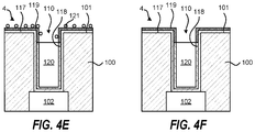
- FIGS. 4A-4F schematically shows a method for selective metal formation in a recessed feature according to another embodiment of the invention.
- FIG. 1A has been reproduced as patterned substrate 4 in FIG. 4A .
- the method includes providing the patterned substrate 4 containing a recessed feature 110 formed in a material.
- the material can include a first layer 100 and a second layer 102 that is exposed in the recessed feature 110 .
- the method further includes depositing a metal oxide layer 117 on the patterned substrate 4 , including in the recessed feature 110 and on the field area 101 around the recessed feature 110 .
- the metal oxide layer 117 may be conformal, and in some examples, the metal oxide layer 117 can include Al 2 O 3 , TiO 2 , HfO 2 , or MnO 2 .
- the method further includes nitriding the metal oxide layer 117 on the field area 101 and in the recessed feature 110 to form a nitrided metal oxide layer 118 .
- the nitriding process incorporates nitrogen into at least a surface region of the metal oxide layer 117 .
- the nitrided metal oxide layer 118 may be conformal.
- the step of nitriding the metal oxide layer 117 may be carried out using a thermal nitriding process (e.g., NH 3 anneal in the absence of a plasma) that effectively nitrides at least a portion of the thickness of the entire metal oxide layer 117 , including in the recessed feature 110 .
- a thermal nitriding process e.g., NH 3 anneal in the absence of a plasma
- the method further includes oxidizing the nitrided metal oxide layer 118 on the field area 101 to form an oxidized nitrided metal oxide layer 119 .
- the oxidizing process incorporates oxygen into at least a surface region of the nitrided metal oxide layer 118 .
- the step of oxidizing the nitrated metal oxide layer can be performed using plasma-excited O 2 gas, where the small opening of the recessed feature 110 limits the penetration of the plasma-excited O 2 gas into the recessed feature 110 . This limits the oxidation of the nitrited metal oxide layer to the field area 101 and an upper portion of the recessed feature 110 . This is schematically shown in FIG. 4D .
- the method further includes depositing a metal layer 120 on the patterned substrate 4 by vapor phase deposition, where the metal layer 120 is preferentially deposited on the nitrided metal oxide layer 118 that is not oxidized in the recessed feature 110 .
- the preferential metal deposition is believed to be due to a shorter incubation time for the metal deposition on the nitrated metal oxide layer relative to on the oxidized nitrided metal oxide layer 119 .
- the metal deposition may not be completely selective and metal nuclei 121 may be deposited on the oxidized nitrided metal oxide layer 119 on the field area 101 .
- the metal nuclei 121 may be form a non-continuous layer where the total amount of the metal in the metal nuclei 121 is less than the amount of the metal in the metal layer 120 .
- the metal layer 120 may fully fill the recessed feature 110 where oxidation of the nitrided metal oxide layer 118 is avoided.
- the method further includes removing the metal nuclei 121 deposited on the field area 101 of the first layer 100 around the recessed feature 110 to selectively form the metal layer 120 in the recessed feature 110 .
- the metal layer 120 may not fully fill the recessed feature 110 where oxidation of the nitrided metal oxide layer 118 is avoided, and the steps of depositing and removing may be repeated at least once to increase a thickness of the metal layer 120 deposited in the recessed feature 110 . According to one embodiment, the steps of depositing and removing may be repeated until the recessed feature 110 is fully filled with the metal layer 120 .
- FIGS. 5A-5D schematically shows a method for selective metal formation in a recessed feature according to another embodiment of the invention.
- FIG. 5A shows a patterned substrate 5 containing recessed features 510 formed in a material 500 , where the recessed features contain sidewalls 503 and bottom 502 .
- the method includes depositing a metal oxide layer 504 on the patterned substrate 5 , including in the recessed features 510 and on a field area 501 around the recessed features 510 . This is schematically shown in FIG. 5B .
- the method further includes nitriding the metal oxide layer 504 on the field area 101 .
- the nitriding process incorporates nitrogen into at least a surface region of the metal oxide layer 504 to form a nitrided metal oxide layer 505 .
- This is schematically shown in FIG. 5C .
- the step of nitriding the metal oxide layer 504 can be performed using plasma-excited nitrogen-containing gas (e.g., N 2 or NH 3 ), where the small openings of the recessed features 510 limit the penetration of the plasma-excited nitrogen-containing gas into the recessed features 510 .
- plasma-excited nitrogen-containing gas e.g., N 2 or NH 3
- the method further includes depositing a metal layer 506 on the patterned substrate 5 by vapor phase deposition, where the metal layer 506 is preferentially deposited on the nitrided metal oxide layer 505 on the field area 501 .
- the metal deposition may not be completely selective and metal nuclei 507 may be deposited on the metal oxide layer 504 in the recessed features 510 .
- the method further includes removing the metal nuclei 507 deposited in the recessed features 510 to selectively form the metal layer 506 on the field area 501 . This is schematically shown in FIG. 5E .
- the steps of depositing and removing may be repeated at least once to increase a thickness of the metal layer 506 on the field area 501 .
- FIGS. 6A-6D schematically shows a method for selective metal formation in a recessed feature according to another embodiment of the invention.
- the patterned substrate 6 may include a portion of a 3D NAND device.
- the method include providing a patterned substrate 6 containing an etched vertical feature 610 and etched horizontal features 601 in a material 600 .
- the etched vertical feature 610 may be tapered with a larger opening near the top than near the bottom.
- the material 600 may include SiO 2 or SiN.
- the method further includes nitriding the etched vertical feature 610 and the etched horizontal features 601 to form a nitrided layer 602 .
- the process of nitriding can include a thermal nitriding process (e.g., NH 3 anneal in the absence of a plasma) that nitrides both the etched vertical feature 610 and etched horizontal features 601 . Thereafter, the method includes a plasma treatment (e.g., an Ar plasma) that removes the nitrided layer 602 from the etched vertical feature 610 , while retaining the nitrided layer 602 in the etched horizontal features 601 .
- a plasma treatment e.g., an Ar plasma
- the method further includes depositing a metal layer 603 on the patterned substrate 6 by vapor phase deposition, where the metal layer 603 is preferentially deposited on the nitrided layer 602 in the etched horizontal features 601 relative to on the etched vertical feature 610 . This is shown in FIG. 6C .
- the vapor phase deposition is performed until the etched vertical feature 610 is also fully filled with a metal layer 604 .
- the selective metal deposition is due to a higher metal deposition rate on the nitrided layer 602 than on the etched vertical feature 610 that is not nitrided. This allows for complete metal filling of the etched vertical feature 610 and the etched horizontal features 601 without any voids.
Landscapes
- Internal Circuitry In Semiconductor Integrated Circuit Devices (AREA)
- Electrodes Of Semiconductors (AREA)
- Physics & Mathematics (AREA)
- Engineering & Computer Science (AREA)
- Plasma & Fusion (AREA)
- Formation Of Insulating Films (AREA)
- Semiconductor Memories (AREA)
- Non-Volatile Memory (AREA)
- Chemical Vapour Deposition (AREA)
Priority Applications (2)
| Application Number | Priority Date | Filing Date | Title |
|---|---|---|---|
| US16/598,772 US11024535B2 (en) | 2018-10-10 | 2019-10-10 | Method for filling recessed features in semiconductor devices with a low-resistivity metal |
| US17/334,389 US11621190B2 (en) | 2018-10-10 | 2021-05-28 | Method for filling recessed features in semiconductor devices with a low-resistivity metal |
Applications Claiming Priority (2)
| Application Number | Priority Date | Filing Date | Title |
|---|---|---|---|
| US201862744038P | 2018-10-10 | 2018-10-10 | |
| US16/598,772 US11024535B2 (en) | 2018-10-10 | 2019-10-10 | Method for filling recessed features in semiconductor devices with a low-resistivity metal |
Related Child Applications (1)
| Application Number | Title | Priority Date | Filing Date |
|---|---|---|---|
| US17/334,389 Division US11621190B2 (en) | 2018-10-10 | 2021-05-28 | Method for filling recessed features in semiconductor devices with a low-resistivity metal |
Publications (2)
| Publication Number | Publication Date |
|---|---|
| US20200118871A1 US20200118871A1 (en) | 2020-04-16 |
| US11024535B2 true US11024535B2 (en) | 2021-06-01 |
Family
ID=70160709
Family Applications (2)
| Application Number | Title | Priority Date | Filing Date |
|---|---|---|---|
| US16/598,772 Active US11024535B2 (en) | 2018-10-10 | 2019-10-10 | Method for filling recessed features in semiconductor devices with a low-resistivity metal |
| US17/334,389 Active 2039-11-22 US11621190B2 (en) | 2018-10-10 | 2021-05-28 | Method for filling recessed features in semiconductor devices with a low-resistivity metal |
Family Applications After (1)
| Application Number | Title | Priority Date | Filing Date |
|---|---|---|---|
| US17/334,389 Active 2039-11-22 US11621190B2 (en) | 2018-10-10 | 2021-05-28 | Method for filling recessed features in semiconductor devices with a low-resistivity metal |
Country Status (6)
| Country | Link |
|---|---|
| US (2) | US11024535B2 (https=) |
| JP (1) | JP7406684B2 (https=) |
| KR (1) | KR102759932B1 (https=) |
| CN (1) | CN112805818B (https=) |
| TW (1) | TWI835883B (https=) |
| WO (1) | WO2020077112A1 (https=) |
Cited By (3)
| Publication number | Priority date | Publication date | Assignee | Title |
|---|---|---|---|---|
| US20220139776A1 (en) * | 2020-11-03 | 2022-05-05 | Tokyo Electron Limited | Method for filling recessed features in semiconductor devices with a low-resistivity metal |
| US11621190B2 (en) | 2018-10-10 | 2023-04-04 | Tokyo Electron Limited | Method for filling recessed features in semiconductor devices with a low-resistivity metal |
| WO2023164685A1 (en) * | 2022-02-28 | 2023-08-31 | Tokyo Electron Limited | Selective inhibition for selective metal deposition |
Families Citing this family (8)
| Publication number | Priority date | Publication date | Assignee | Title |
|---|---|---|---|---|
| US11823896B2 (en) * | 2019-02-22 | 2023-11-21 | Taiwan Semiconductor Manufacturing Co., Ltd. | Conductive structure formed by cyclic chemical vapor deposition |
| US12507408B2 (en) | 2020-03-12 | 2025-12-23 | Tokyo Electron Limited | Method and structures to reduce resistivity in three-dimensional structures for microelectronic workpieces using material deposited in recesses at edges of holes in a multilayer stack |
| WO2022169567A1 (en) * | 2021-02-05 | 2022-08-11 | Tokyo Electron Limited | Removal of stray ruthenium metal nuclei for selective ruthenium metal layer formation |
| KR20230156342A (ko) * | 2021-03-16 | 2023-11-14 | 도쿄엘렉트론가부시키가이샤 | 반도체 디바이스의 함입형 형상부를 저-저항률 금속으로 충전하기 위한 방법 |
| JP2024523510A (ja) | 2021-07-06 | 2024-06-28 | 東京エレクトロン株式会社 | 自己組織化単分子層を使用する選択的な膜形成 |
| US12598977B2 (en) * | 2021-12-21 | 2026-04-07 | Intel Corporation | Fill of vias in single and dual damascene structures using self-assembled monolayer |
| JP7803157B2 (ja) * | 2022-02-14 | 2026-01-21 | 東京エレクトロン株式会社 | 凹部にルテニウムを埋め込む方法、及び装置 |
| US20240431025A1 (en) * | 2023-06-26 | 2024-12-26 | International Business Machines Corporation | Corrosion resistant single damascene interconnects |
Citations (11)
| Publication number | Priority date | Publication date | Assignee | Title |
|---|---|---|---|---|
| US5723358A (en) * | 1996-04-29 | 1998-03-03 | Vlsi Technology, Inc. | Method of manufacturing amorphous silicon antifuse structures |
| US6492263B1 (en) | 2000-06-29 | 2002-12-10 | Mosel Vitelic, Inc. | Dual damascene process which prevents diffusion of metals and improves trench-to-via alignment |
| US20050031786A1 (en) | 2001-05-22 | 2005-02-10 | Novellus Systems, Inc. | Method for reducing tungsten film roughness and improving step coverage |
| KR20080001254A (ko) | 2006-06-29 | 2008-01-03 | 삼성전자주식회사 | 반도체 소자의 금속 배선 형성 방법 |
| US20080090409A1 (en) * | 2006-10-11 | 2008-04-17 | Elpida Memory, Inc. | Method for manufacturing a semiconductor device including interconnections having a smaller width |
| US20090085211A1 (en) * | 2007-09-28 | 2009-04-02 | Tokyo Electron Limited | Electrical contacts for integrated circuits and methods of forming using gas cluster ion beam processing |
| US20090305480A1 (en) * | 2008-06-09 | 2009-12-10 | Tokyo Electron Limited | Semiconductor device manufacturing method and storage medium |
| US20120213941A1 (en) | 2011-02-22 | 2012-08-23 | Varian Semiconductor Equipment Associates, Inc. | Ion-assisted plasma treatment of a three-dimensional structure |
| US20120302071A1 (en) | 2008-08-13 | 2012-11-29 | Synos Technology, Inc. | Forming Substrate Structure by Filling Recesses with Deposition Material |
| US20160351568A1 (en) * | 2015-05-29 | 2016-12-01 | Taiwan Semiconductor Manufacturing Co., Ltd. | Structure and formation method of semiconductor device structure |
| US20190164887A1 (en) * | 2017-11-30 | 2019-05-30 | Taiwan Semiconductor Manufacturing Company, Ltd. | Interconnect Structures and Methods of Forming the Same |
Family Cites Families (30)
| Publication number | Priority date | Publication date | Assignee | Title |
|---|---|---|---|---|
| JPS62216224A (ja) * | 1986-03-17 | 1987-09-22 | Fujitsu Ltd | タングステンの選択成長方法 |
| NL8801917A (nl) * | 1988-08-02 | 1990-03-01 | Hollandse Signaalapparaten Bv | Koerscorrectiesysteem voor in baan corrigeerbare voorwerpen. |
| JPH03132024A (ja) * | 1989-10-18 | 1991-06-05 | Sanyo Electric Co Ltd | 半導体装置の製造方法 |
| JP3038875B2 (ja) * | 1990-10-18 | 2000-05-08 | 日本電気株式会社 | 半導体装置の製造方法 |
| JPH0513367A (ja) * | 1991-07-03 | 1993-01-22 | Hitachi Ltd | 半導体集積回路装置の製造方法 |
| JPH05166754A (ja) * | 1991-12-18 | 1993-07-02 | Sharp Corp | 半導体装置の製造方法 |
| JPH0982798A (ja) * | 1995-09-12 | 1997-03-28 | Toshiba Corp | 半導体装置およびその製造方法 |
| US6040243A (en) * | 1999-09-20 | 2000-03-21 | Chartered Semiconductor Manufacturing Ltd. | Method to form copper damascene interconnects using a reverse barrier metal scheme to eliminate copper diffusion |
| US6787460B2 (en) * | 2002-01-14 | 2004-09-07 | Samsung Electronics Co., Ltd. | Methods of forming metal layers in integrated circuit devices using selective deposition on edges of recesses and conductive contacts so formed |
| KR100455382B1 (ko) * | 2002-03-12 | 2004-11-06 | 삼성전자주식회사 | 듀얼 다마신 구조를 가지는 반도체 소자의 금속 배선 형성방법 |
| US6797642B1 (en) * | 2002-10-08 | 2004-09-28 | Novellus Systems, Inc. | Method to improve barrier layer adhesion |
| US20040121583A1 (en) * | 2002-12-19 | 2004-06-24 | Taiwan Semiconductor Manufacturing Co., Ltd. | Method for forming capping barrier layer over copper feature |
| US7365001B2 (en) * | 2003-12-16 | 2008-04-29 | International Business Machines Corporation | Interconnect structures and methods of making thereof |
| KR100609049B1 (ko) * | 2004-12-06 | 2006-08-09 | 주식회사 하이닉스반도체 | 반도체 소자의 금속배선 형성방법 |
| US20060246699A1 (en) * | 2005-03-18 | 2006-11-02 | Weidman Timothy W | Process for electroless copper deposition on a ruthenium seed |
| KR100640662B1 (ko) * | 2005-08-06 | 2006-11-01 | 삼성전자주식회사 | 장벽금속 스페이서를 구비하는 반도체 소자 및 그 제조방법 |
| US7659197B1 (en) * | 2007-09-21 | 2010-02-09 | Novellus Systems, Inc. | Selective resputtering of metal seed layers |
| KR101604054B1 (ko) * | 2009-09-03 | 2016-03-16 | 삼성전자주식회사 | 반도체 소자 및 그 형성방법 |
| US8945305B2 (en) * | 2010-08-31 | 2015-02-03 | Micron Technology, Inc. | Methods of selectively forming a material using parylene coating |
| CN102543835B (zh) * | 2010-12-15 | 2015-05-13 | 中国科学院微电子研究所 | 开口的填充方法 |
| WO2013095433A1 (en) * | 2011-12-21 | 2013-06-27 | Intel Corporation | Electroless filled conductive structures |
| US9895715B2 (en) * | 2014-02-04 | 2018-02-20 | Asm Ip Holding B.V. | Selective deposition of metals, metal oxides, and dielectrics |
| US10049921B2 (en) * | 2014-08-20 | 2018-08-14 | Lam Research Corporation | Method for selectively sealing ultra low-k porous dielectric layer using flowable dielectric film formed from vapor phase dielectric precursor |
| US10014213B2 (en) * | 2015-10-15 | 2018-07-03 | Tokyo Electron Limited | Selective bottom-up metal feature filling for interconnects |
| US9899258B1 (en) * | 2016-09-30 | 2018-02-20 | Taiwan Semiconductor Manufacturing Company, Ltd. | Metal liner overhang reduction and manufacturing method thereof |
| CN107978553B (zh) * | 2016-10-21 | 2020-12-18 | 中芯国际集成电路制造(上海)有限公司 | 一种半导体器件及其制造方法 |
| TWI750352B (zh) * | 2017-03-31 | 2021-12-21 | 日商東京威力科創股份有限公司 | 鍍膜處理方法,鍍膜處理系統及記憶媒體 |
| US10847413B2 (en) * | 2017-11-30 | 2020-11-24 | Taiwan Semiconductor Manufacturing Company, Ltd. | Method of forming contact plugs for semiconductor device |
| US11319334B2 (en) * | 2017-12-28 | 2022-05-03 | Intel Corporation | Site-selective metal plating onto a package dielectric |
| CN112805818B (zh) | 2018-10-10 | 2024-10-18 | 东京毅力科创株式会社 | 用低电阻率金属填充半导体器件中的凹陷特征的方法 |
-
2019
- 2019-10-10 CN CN201980066266.7A patent/CN112805818B/zh active Active
- 2019-10-10 WO PCT/US2019/055676 patent/WO2020077112A1/en not_active Ceased
- 2019-10-10 JP JP2021519654A patent/JP7406684B2/ja active Active
- 2019-10-10 KR KR1020217012312A patent/KR102759932B1/ko active Active
- 2019-10-10 US US16/598,772 patent/US11024535B2/en active Active
- 2019-10-14 TW TW108136852A patent/TWI835883B/zh active
-
2021
- 2021-05-28 US US17/334,389 patent/US11621190B2/en active Active
Patent Citations (13)
| Publication number | Priority date | Publication date | Assignee | Title |
|---|---|---|---|---|
| US5723358A (en) * | 1996-04-29 | 1998-03-03 | Vlsi Technology, Inc. | Method of manufacturing amorphous silicon antifuse structures |
| US6492263B1 (en) | 2000-06-29 | 2002-12-10 | Mosel Vitelic, Inc. | Dual damascene process which prevents diffusion of metals and improves trench-to-via alignment |
| US20050031786A1 (en) | 2001-05-22 | 2005-02-10 | Novellus Systems, Inc. | Method for reducing tungsten film roughness and improving step coverage |
| KR101168768B1 (ko) | 2003-08-26 | 2012-07-25 | 노벨러스 시스템즈, 인코포레이티드 | 텅스텐 박막의 거칠기를 감소시키며 스텝 커버리지를개선하는 방법 |
| KR20080001254A (ko) | 2006-06-29 | 2008-01-03 | 삼성전자주식회사 | 반도체 소자의 금속 배선 형성 방법 |
| US20080090409A1 (en) * | 2006-10-11 | 2008-04-17 | Elpida Memory, Inc. | Method for manufacturing a semiconductor device including interconnections having a smaller width |
| US20090085211A1 (en) * | 2007-09-28 | 2009-04-02 | Tokyo Electron Limited | Electrical contacts for integrated circuits and methods of forming using gas cluster ion beam processing |
| US20090305480A1 (en) * | 2008-06-09 | 2009-12-10 | Tokyo Electron Limited | Semiconductor device manufacturing method and storage medium |
| US20120302071A1 (en) | 2008-08-13 | 2012-11-29 | Synos Technology, Inc. | Forming Substrate Structure by Filling Recesses with Deposition Material |
| US20120213941A1 (en) | 2011-02-22 | 2012-08-23 | Varian Semiconductor Equipment Associates, Inc. | Ion-assisted plasma treatment of a three-dimensional structure |
| KR20140009354A (ko) | 2011-02-22 | 2014-01-22 | 베리안 세미콘덕터 이큅먼트 어소시에이츠, 인크. | 3 차원 구조의 이온 보조 플라즈마 처리 |
| US20160351568A1 (en) * | 2015-05-29 | 2016-12-01 | Taiwan Semiconductor Manufacturing Co., Ltd. | Structure and formation method of semiconductor device structure |
| US20190164887A1 (en) * | 2017-11-30 | 2019-05-30 | Taiwan Semiconductor Manufacturing Company, Ltd. | Interconnect Structures and Methods of Forming the Same |
Non-Patent Citations (1)
| Title |
|---|
| Korean Intellectual Property Office, International Search Report and Written Opinion for international application No. PCT/US2019/055676, dated Feb. 5, 2020, 17 pages. |
Cited By (4)
| Publication number | Priority date | Publication date | Assignee | Title |
|---|---|---|---|---|
| US11621190B2 (en) | 2018-10-10 | 2023-04-04 | Tokyo Electron Limited | Method for filling recessed features in semiconductor devices with a low-resistivity metal |
| US20220139776A1 (en) * | 2020-11-03 | 2022-05-05 | Tokyo Electron Limited | Method for filling recessed features in semiconductor devices with a low-resistivity metal |
| WO2023164685A1 (en) * | 2022-02-28 | 2023-08-31 | Tokyo Electron Limited | Selective inhibition for selective metal deposition |
| US12588435B2 (en) | 2022-02-28 | 2026-03-24 | Tokyo Electron Limited | Selective inhibition for selective metal deposition |
Also Published As
| Publication number | Publication date |
|---|---|
| KR20210057185A (ko) | 2021-05-20 |
| TW202029286A (zh) | 2020-08-01 |
| TWI835883B (zh) | 2024-03-21 |
| CN112805818A (zh) | 2021-05-14 |
| US20210287936A1 (en) | 2021-09-16 |
| JP7406684B2 (ja) | 2023-12-28 |
| WO2020077112A1 (en) | 2020-04-16 |
| KR102759932B1 (ko) | 2025-01-23 |
| CN112805818B (zh) | 2024-10-18 |
| JP2022504574A (ja) | 2022-01-13 |
| US11621190B2 (en) | 2023-04-04 |
| US20200118871A1 (en) | 2020-04-16 |
Similar Documents
| Publication | Publication Date | Title |
|---|---|---|
| US11621190B2 (en) | Method for filling recessed features in semiconductor devices with a low-resistivity metal | |
| KR102524573B1 (ko) | SiOCN 박막들의 형성 | |
| KR102376352B1 (ko) | 다공성의 낮은 유전상수 필름 상에 기공 밀봉 층을 제공하기 위한 방법 및 조성물 | |
| TWI810617B (zh) | 形成及沈積碳氧化矽薄膜的方法 | |
| TWI686499B (zh) | 金屬、金屬氧化物與介電質的選擇性沉積 | |
| US20070287301A1 (en) | Method to minimize wet etch undercuts and provide pore sealing of extreme low k (k<2.5) dielectrics | |
| JP5174435B2 (ja) | ウェットエッチングアンダカットを最小にし且つ超低k(k<2.5)誘電体をポアシーリングする方法 | |
| US20220139776A1 (en) | Method for filling recessed features in semiconductor devices with a low-resistivity metal | |
| KR20080047456A (ko) | 반도체 디바이스용 구조체 및 그의 제조 방법 | |
| US12237216B2 (en) | Method for filling recessed features in semiconductor devices with a low-resistivity metal |
Legal Events
| Date | Code | Title | Description |
|---|---|---|---|
| FEPP | Fee payment procedure |
Free format text: ENTITY STATUS SET TO UNDISCOUNTED (ORIGINAL EVENT CODE: BIG.); ENTITY STATUS OF PATENT OWNER: LARGE ENTITY |
|
| AS | Assignment |
Owner name: TOKYO ELECTRON LIMITED, JAPAN Free format text: ASSIGNMENT OF ASSIGNORS INTEREST;ASSIGNORS:YU, KAI-HUNG;O'MEARA, DAVID;JOY, NICHOLAS;AND OTHERS;SIGNING DATES FROM 20191108 TO 20191112;REEL/FRAME:050981/0076 |
|
| STPP | Information on status: patent application and granting procedure in general |
Free format text: NON FINAL ACTION MAILED |
|
| STPP | Information on status: patent application and granting procedure in general |
Free format text: RESPONSE TO NON-FINAL OFFICE ACTION ENTERED AND FORWARDED TO EXAMINER |
|
| STPP | Information on status: patent application and granting procedure in general |
Free format text: NOTICE OF ALLOWANCE MAILED -- APPLICATION RECEIVED IN OFFICE OF PUBLICATIONS |
|
| STPP | Information on status: patent application and granting procedure in general |
Free format text: PUBLICATIONS -- ISSUE FEE PAYMENT VERIFIED |
|
| STCF | Information on status: patent grant |
Free format text: PATENTED CASE |
|
| MAFP | Maintenance fee payment |
Free format text: PAYMENT OF MAINTENANCE FEE, 4TH YEAR, LARGE ENTITY (ORIGINAL EVENT CODE: M1551); ENTITY STATUS OF PATENT OWNER: LARGE ENTITY Year of fee payment: 4 |