US10827599B2 - Piezoelectric transformer - Google Patents
Piezoelectric transformer Download PDFInfo
- Publication number
- US10827599B2 US10827599B2 US15/327,642 US201515327642A US10827599B2 US 10827599 B2 US10827599 B2 US 10827599B2 US 201515327642 A US201515327642 A US 201515327642A US 10827599 B2 US10827599 B2 US 10827599B2
- Authority
- US
- United States
- Prior art keywords
- piezoelectric transformer
- output
- region
- face
- transformer according
- Prior art date
- Legal status (The legal status is an assumption and is not a legal conclusion. Google has not performed a legal analysis and makes no representation as to the accuracy of the status listed.)
- Active, expires
Links
- 239000000463 material Substances 0.000 claims abstract description 27
- 230000005684 electric field Effects 0.000 claims abstract description 23
- 238000009413 insulation Methods 0.000 claims description 37
- 238000005488 sandblasting Methods 0.000 claims description 6
- 229920000642 polymer Polymers 0.000 claims description 4
- 239000002966 varnish Substances 0.000 claims description 4
- 229920001296 polysiloxane Polymers 0.000 claims description 3
- 239000011248 coating agent Substances 0.000 claims 1
- 238000000576 coating method Methods 0.000 claims 1
- 210000002381 plasma Anatomy 0.000 description 32
- 239000007789 gas Substances 0.000 description 7
- 238000000034 method Methods 0.000 description 5
- 239000000758 substrate Substances 0.000 description 4
- 230000008901 benefit Effects 0.000 description 3
- 238000006243 chemical reaction Methods 0.000 description 3
- 230000000694 effects Effects 0.000 description 3
- 239000007788 liquid Substances 0.000 description 3
- 230000003213 activating effect Effects 0.000 description 2
- 230000005284 excitation Effects 0.000 description 2
- 230000009467 reduction Effects 0.000 description 2
- 230000004044 response Effects 0.000 description 2
- 239000004831 Hot glue Substances 0.000 description 1
- CBENFWSGALASAD-UHFFFAOYSA-N Ozone Chemical compound [O-][O+]=O CBENFWSGALASAD-UHFFFAOYSA-N 0.000 description 1
- QVGXLLKOCUKJST-UHFFFAOYSA-N atomic oxygen Chemical compound [O] QVGXLLKOCUKJST-UHFFFAOYSA-N 0.000 description 1
- 238000005266 casting Methods 0.000 description 1
- 230000008859 change Effects 0.000 description 1
- 230000003247 decreasing effect Effects 0.000 description 1
- 230000001419 dependent effect Effects 0.000 description 1
- 230000006872 improvement Effects 0.000 description 1
- 230000001788 irregular Effects 0.000 description 1
- 238000004519 manufacturing process Methods 0.000 description 1
- 229910052760 oxygen Inorganic materials 0.000 description 1
- 239000001301 oxygen Substances 0.000 description 1
- 230000010287 polarization Effects 0.000 description 1
- 229920006254 polymer film Polymers 0.000 description 1
- 238000005245 sintering Methods 0.000 description 1
- 238000005507 spraying Methods 0.000 description 1
Images


Classifications
-
- H—ELECTRICITY
- H10—SEMICONDUCTOR DEVICES; ELECTRIC SOLID-STATE DEVICES NOT OTHERWISE PROVIDED FOR
- H10N—ELECTRIC SOLID-STATE DEVICES NOT OTHERWISE PROVIDED FOR
- H10N30/00—Piezoelectric or electrostrictive devices
- H10N30/40—Piezoelectric or electrostrictive devices with electrical input and electrical output, e.g. functioning as transformers
-
- H—ELECTRICITY
- H01—ELECTRIC ELEMENTS
- H01F—MAGNETS; INDUCTANCES; TRANSFORMERS; SELECTION OF MATERIALS FOR THEIR MAGNETIC PROPERTIES
- H01F38/00—Adaptations of transformers or inductances for specific applications or functions
-
- H01L41/047—
-
- H01L41/0533—
-
- H01L41/107—
-
- H—ELECTRICITY
- H05—ELECTRIC TECHNIQUES NOT OTHERWISE PROVIDED FOR
- H05H—PLASMA TECHNIQUE; PRODUCTION OF ACCELERATED ELECTRICALLY-CHARGED PARTICLES OR OF NEUTRONS; PRODUCTION OR ACCELERATION OF NEUTRAL MOLECULAR OR ATOMIC BEAMS
- H05H1/00—Generating plasma; Handling plasma
- H05H1/24—Generating plasma
- H05H1/2475—Generating plasma using acoustic pressure discharges
- H05H1/2481—Generating plasma using acoustic pressure discharges the plasma being activated using piezoelectric actuators
-
- H—ELECTRICITY
- H10—SEMICONDUCTOR DEVICES; ELECTRIC SOLID-STATE DEVICES NOT OTHERWISE PROVIDED FOR
- H10N—ELECTRIC SOLID-STATE DEVICES NOT OTHERWISE PROVIDED FOR
- H10N30/00—Piezoelectric or electrostrictive devices
- H10N30/20—Piezoelectric or electrostrictive devices with electrical input and mechanical output, e.g. functioning as actuators or vibrators
-
- H—ELECTRICITY
- H10—SEMICONDUCTOR DEVICES; ELECTRIC SOLID-STATE DEVICES NOT OTHERWISE PROVIDED FOR
- H10N—ELECTRIC SOLID-STATE DEVICES NOT OTHERWISE PROVIDED FOR
- H10N30/00—Piezoelectric or electrostrictive devices
- H10N30/80—Constructional details
-
- H—ELECTRICITY
- H10—SEMICONDUCTOR DEVICES; ELECTRIC SOLID-STATE DEVICES NOT OTHERWISE PROVIDED FOR
- H10N—ELECTRIC SOLID-STATE DEVICES NOT OTHERWISE PROVIDED FOR
- H10N30/00—Piezoelectric or electrostrictive devices
- H10N30/80—Constructional details
- H10N30/87—Electrodes or interconnections, e.g. leads or terminals
-
- H—ELECTRICITY
- H10—SEMICONDUCTOR DEVICES; ELECTRIC SOLID-STATE DEVICES NOT OTHERWISE PROVIDED FOR
- H10N—ELECTRIC SOLID-STATE DEVICES NOT OTHERWISE PROVIDED FOR
- H10N30/00—Piezoelectric or electrostrictive devices
- H10N30/80—Constructional details
- H10N30/88—Mounts; Supports; Enclosures; Casings
- H10N30/883—Further insulation means against electrical, physical or chemical damage, e.g. protective coatings
-
- H05H2001/2481—
Definitions
- the present invention relates to a piezoelectric transformer.
- the piezoelectric transformer can be used, in particular, in a device for generating atmospheric-pressure plasmas.
- a piezoelectric transformer is a design of a tuned transformer which is based on piezoelectricity and, in contrast to conventional magnetic transformers, is an electromechanical system.
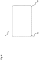
- FIG. 1 shows a piezoelectric transformer 1 which is also known as a Rosen-type transformer.
- the piezoelectric transformer 1 comprises an input region 2 and an output region 3 .
- the piezoelectric transformer 1 comprises electrodes 4 , to which an alternating voltage can be applied.
- the electrodes 4 extend in a longitudinal direction L of the piezoelectric transformer 1 .
- the electrodes 4 are stacked in alternation with a piezoelectric material 5 in a stacking direction S which is perpendicular to the longitudinal direction L.
- the piezoelectric material 5 is polarized in the stacking direction S in this case.
- the electrodes 4 are situated in the interior of the piezoelectric transformer 1 and are also referred to as internal electrodes.
- the piezoelectric transformer 1 has a first longitudinal side 6 and a second longitudinal side 7 which is opposite the first longitudinal side 6 .
- a first external electrode 8 is situated on the first longitudinal side 6 .
- a second external electrode (not shown) is situated on the second longitudinal side 7 .
- the internal electrodes 4 are electrically contacted, in the stacking direction S, in alternation with either the first external electrode 8 or the second external electrode.
- the input region 2 can be controlled by means of a low alternating voltage which is applied between the electrodes 4 . Due to the piezoelectric effect, the alternating voltage applied on the input side is initially converted into a mechanical vibration. The frequency of the mechanical vibration is essentially dependent, in this case, on the geometry and the mechanical design of the piezoelectric transformer 1 .
- the output region 3 comprises piezoelectric material 9 and is free from internal electrodes.
- the piezoelectric material 9 in the output region is polarized in the longitudinal direction L.
- the piezoelectric material 9 of the output region 3 can be the same material as the piezoelectric material 5 of the input region 2 , wherein the piezoelectric materials 5 and 9 can differ in terms of the polarization direction thereof.
- the output region 3 comprises an output-side end face 10 which is metallized and forms an output electrode.
- the electrical voltage generated in the output region 3 is therefore present between the metallized end face 10 and the end of the electrodes 4 of the input region 2 .
- a high voltage is present at the output-side end face 10 in this case.
- the piezoelectric transformer 1 generates high electrical fields which are capable of ionizing gasses by means of electrical excitation.
- atoms or molecules of the particular gas are ionized and form a plasma. Ionization always takes place when the electrical field strength on the surface of the piezoelectric transformer 1 exceeds the ignition field strength of the plasma.
- the ignition field strength of a plasma is the field strength required for ionizing the atoms or molecules.
- FIG. 1 An ignition 11 of plasma on the output-side end face and further ignitions 12 of plasma on the lateral edges 13 are indicated in FIG. 1 .
- the problem addressed by the present invention is therefore that of providing an improved piezoelectric transformer which has a longer service life, for example.
- a piezoelectric transformer is provided, which is divided in the longitudinal direction into an input region and an output region, wherein electrodes and piezoelectric material are alternately stacked in the input region and an alternating voltage can be applied to the electrodes in the input region, wherein the output region comprises piezoelectric material which effectuates the build-up of an electrical field when alternating voltage is applied in the input region, wherein the piezoelectric transformer has an output-side end face which faces away from the input region, and has lateral edges which extend in the longitudinal direction, and wherein the piezoelectric transformer is designed for ionizing atoms or molecules at the output-side end face, thereby avoiding ionization of atoms or molecules at the lateral edges.
- the piezoelectric transformer can be the above-described Rosen-type transformer, wherein, in addition, measures are provided for avoiding the ionization of atoms or molecules at the lateral edges. All the structural and functional features which were disclosed in connection with the Rosen-type transformer can also be present in the piezoelectric transformer according to the invention.
- the input region can comprise electrodes and piezoelectric material which are stacked in alternation in a stacking direction.
- the stacking direction is perpendicular to the longitudinal direction in this case.
- the stacking direction is furthermore perpendicular to the surface normal of the first longitudinal side 6 on which the first external electrode 8 is situated.
- the output region is free from internal electrodes.
- the output region is a monolithic stack comprising the piezoelectric material, wherein the output-side end face can be metallized.
- the output region comprises piezoelectric material which is polarized in the longitudinal direction.
- the input region is also referred to as an excitation zone and the output region is also referred to as a high-voltage zone.
- the piezoelectric transformer has an essentially cuboid shape.
- the longitudinal direction is defined by the connection of the outer surfaces of the piezoelectric transformer located furthest apart from one another, i.e., as the direction along the longest edge of the piezoelectric transformer.
- the electrical field strength reaches its maximum at the output-side end face.
- the lateral edges can therefore be modified in such a way that the field strength of the electrical field is specifically reduced here and, in particular, the occurrence of stress peaks is avoided.
- the electrical field strength on the lateral edges should lie below the ignition field strength of the plasma when the electrical field strength on the output-side end face reaches the ignition field strength.
- the lateral edges of the piezoelectric transformer can have a rounded region. Stress peaks are avoided in this rounded region, and so an ionization of atoms or molecules does not take place on the lateral edges. Due to the rounding of the edges, the electrical field strength is reduced on the surface of the lateral edge.
- the edges can be rounded before or after sintering.
- the rounded region can extend at least from the output-side end face up to the middle of the output region.
- the greatest electrical field strength is present in this region during the operation of the piezoelectric transformer. It is important, therefore, to reduce the field strength at the edges in this region, in particular, in order to avoid an undesirable ignition of a plasma.
- the rounded region directly adjoins the output-side end face, since the danger of undesirable ionizations on the lateral edges is particularly great close to the output-side end face.
- the rounded region can extend along the entire length of the lateral edges. In certain methods for manufacturing the rounded region, for example, rubbing, it is substantially easier to round the lateral edges along the entire length thereof. A rounding of the lateral edges in the input region as well does not negatively influence the functionality of the piezoelectric transformer.
- the lateral edges can have a radius between 0.1 mm and 3 mm in the rounded region. If the radius were selected to be less than 0.1 mm, a sufficient reduction of the electrical field strength on the lateral edges would no longer be ensured, since this reduction would be approximately angular in this case. A rounding having a radius of 3 mm is more than sufficient in order to adequately reduce the electrical field strength at the edges, and so a rounding having an even larger radius would not result in a further improvement of the behavior of the piezoelectric transformer.
- the range for the radius between 0.1 mm and 3 mm is therefore optimal.
- the radius can furthermore lie between 0.2 mm to 1.0 mm.
- the rounded region of the lateral edges can be rounded, for example, by means of rubbing, grinding, or sandblasting.
- rubbing refers to a method in which all edges of the piezoelectric transformer, in the unsintered, green state thereof, are rubbed off by means of loose grain.
- a multitude of piezoelectric transformers can be placed in a drum along with a rubbing means and, therein, can be rubbed against each other, whereby the edges are rounded off. The advantages of rubbing are that this method can be carried out very quickly and cost-effectively.
- the edges and corners of the output-side end face are also rounded off.
- a piezoelectric transformer is thereby obtained, which has a rounded, output-side end face, in the case of which ionization takes place only on the corners of the end face. Due to the rounding, the corners of the end face have an enlarged surface, and so a widely fanned plasma jet results. This can be advantageous for certain applications. If a fanning of the plasma jet is not desirable for the application, the end face can be ground after the rubbing, whereby the rounded edges of the end face become angular again.
- grinding refers to a method in which a grinding disk is utilized on the piezoelectric transformer in the sintered state thereof.
- the piezoelectric transformer can be treated highly precisely in this case.
- the edges on the end face can be left untreated.
- Grinding offers great flexibility in terms of design.
- the rounded region can be configured by means of grinding in such a way that said region has a decreasing radius.
- the radius of the rounded region can be maximal on the output-side end face and can decrease toward the input side. Grinding also makes it possible to bring the end face into a desired shape.
- the end face can be designed, for example, to be hemispherical or to taper to a point in the manner of a pyramid.
- the configuration of the end face determines the shape of the plasma jet which can be generated.
- a further advantage of grinding is that this method results in a very smooth surface, and so local field non-uniformities at irregular points cannot occur.
- the lateral edges are blasted with loose grain using compressed air. In this way, material is removed from the lateral edges.
- Sandblasting can be carried out in the sintered state of the piezoelectric transformer.
- the regions of the piezoelectric transformer which are supposed to be left untreated during sandblasting can be covered, for example, masked off, during sandblasting.
- the mass of the piezoelectric transformer is changed only to such a low extent that the vibration response of the piezoelectric transformer does not change.
- the output region can be coated at least partially with an insulation layer.
- the insulation layer reduces the electrical field strength on the surface of the regions covered by the insulation layer.
- the insulation layer can at least partially cover the lateral edges, in particular.
- the insulation layer Due to the insulation layer, it can be ensured, in this way, that the electrical field strength on the surface of the lateral edges is not too great and, therefore, an ionization of atoms and/or molecules on the lateral edges can be prevented.
- the application of the insulation layer can be combined with the rounding of the lateral edges, in order to avoid an undesirable ionization on the lateral edges as a result of the combination of these two measures.
- the insulation layer can have a length which lies in the range from 15% to 45% of the total length of the piezoelectric transformer, preferably in the range from 20% to 30% of the total length.
- the insulation layer can comprise heat shrink tubing.
- the heat shrink tubing can be coated, in particular, with a hot-melt adhesive on the inner side thereof. In this way, the heat shrink tubing can be prevented from coming loose from the piezoelectric transformer, due to vibrations of the piezoelectric transformer during operation, and slipping off the output region.
- the heat shrink tubing can terminate so as to be flush with the output-side end face or can extend beyond the end face.
- an end region of the output region, which adjoins the output-side end face, can also remain free from the heat shrink tubing.
- the heat shrink tubing overhangs slightly, a bundling of the plasma occurs. This is advantageous for applications which utilize the effect of the plasma in order to activate surfaces, for example. If the heat shrink tubing terminates so as to be flush with the piezoelectric transformer or leaves a small end region—which does not exceed 2 mm—of the lateral edges exposed, the plasma is not directed. An operation in an oxygen-containing working gas more ozone therefore results, which can be advantageous for medical applications. The length of the heat shrink tubing should therefore be adapted to the desired purpose.
- the insulation layer can comprise at least one selected from silicone, a cured polymer, or a varnish. These materials can be applied in liquid form as an insulation layer. Liquid casting, application by means of a mold, or spraying is suitable for this purpose.
- the insulation layer should have a sufficient thickness along the lateral edges. When the insulation layer is applied in liquid form, this thickness can be ensured by adjusting the viscosity or by means of multiple applications.
- the end face can be free from the insulation layer. This is important, since an ionization of the atoms or molecules on the end face is desirable and should not be impeded by the insulation layer.
- the insulation layer can have a thickness in the range from 0.1 mm to 3 mm, wherein the thickness preferably lies between 0.2 mm and 1.0 mm. Due to the insulation layer, an additional mass is added to the piezoelectric transformer, whereby the vibration response thereof changes. Therefore, the insulation layer should be selected so as to be as thin as possible. Said insulation layer must be thick enough, however, to reduce the field strength on the surface of the lateral edges to below the ignition field strength of the plasma. These requirements are met with insulation layers having a thickness between 0.1 mm and 3 mm.
- the piezoelectric transformer can be used for generating cold atmospheric plasma.
- the atmospheric-pressure plasmas can be classified into so-called cold, non-thermal plasmas having a gas temperature of typically less than 100° C. and thermal plasmas having higher gas temperatures.
- the present invention relates to cold, non-thermal plasmas which have the advantage that the gas temperature lies in the order of magnitude of room temperature or only slightly above room temperature, and so a longer dwell time of the plasma on a substrate to be treated is also possible and sensitive substrates, e.g., thin polymer films, can also be treated longer with this plasma without the surface of the substrate or the substrate itself becoming damaged.
- the piezoelectric transformer can be a Rosen-type transformer.
- the output-side end face can comprise rounded edges and/or rounded corners.
- the output-side end face can be suitable for generating a widely fanned plasma jet.
- the present invention further relates to a device for generating atmospheric-pressure plasma, which device comprises the above-described piezoelectric transformer which is situated in a gas-filled volume.
- the piezoelectric transformer is therefore used for ionizing the gas and, in this way, generates the plasma.
- Such a device can be used, in particular, for activating or otherwise processing surfaces and for medical applications.
- FIG. 1 shows a piezoelectric transformer which is known in the prior art
- FIG. 2 shows a piezoelectric transformer according to a first exemplary embodiment of the present invention
- FIG. 3 shows a piezoelectric transformer according to a second exemplary embodiment of the present invention
- FIG. 4 shows a cross section through the piezoelectric transformer shown in FIG. 3 .
- FIG. 2 shows a piezoelectric transformer 1 .
- the piezoelectric transformer 1 comprises the first and the second longitudinal sides 6 , 7 as well as a third longitudinal side 16 and a fourth longitudinal side 17 .
- Each of the longitudinal sides 6 , 7 , 16 , 17 extends in the longitudinal direction L.
- Each of the longitudinal sides 6 , 7 , 16 , 17 is furthermore perpendicular to the output-side end face 10 .
- the insulation layer 14 is applied onto the longitudinal sides 6 , 7 , 16 , 17 in this case.
- the output-side end face 10 is free from the insulation layer.
- the material of the insulation layer 14 is selected in such a way, in this case, that an electrical field strength which is present in the interior of the insulation layer 14 is substantially reduced on the outward-facing side of the insulation layer 14 .
- the insulation layer 14 therefore insulates the electrical field.
- the electrical field strength is therefore substantially reduced in the regions of the lateral edges 13 covered by the insulation layer 14 .
- the insulation layer 14 can either be a heat shrink tubing or a layer consisting of silicone, a varnish, or a cured polymer.
- the insulation layer 14 extends from the output-side end face 10 up to a length of one-fourth of the piezoelectric transformer.
- FIG. 3 shows a first exemplary embodiment of a piezoelectric transformer 1 .
- the lateral edges 13 of the piezoelectric transformer 1 have a rounded region 15 in this case.
- the lateral edges 13 are not angular as in the remaining regions, but rather are rounded.
- the rounded region 15 extends along the entire length of the lateral edges 13 .
- the electrical field strength on the lateral edges 13 is distributed over a larger area, and so the occurrence of stress peaks is avoided and the maximum electrical field strength achieved is reduced in the region of the lateral edges 13 .
- the electrical field strength on the lateral edges 13 is reduced to such an extent that the electrical field strength is less than the field strength required for ionizing atoms or molecules.
- FIG. 4 shows a cross section perpendicular to the longitudinal direction L through the piezoelectric transformer 1 shown in FIG. 3 .
- the piezoelectric transformer 1 comprises rounded lateral edges 13 .
- the working frequency of the piezoelectric transformer 1 is essentially determined by the length thereof. If a length of 70 mm is selected, a working frequency of 50 kHz results. This working frequency is suitable, in particular, for activating or processing surfaces. A working frequency of 100 kHz can be advantageous for medical applications. Therefore, a length of the piezoelectric transformer 1 of 35 mm is selected in this case.
Applications Claiming Priority (4)
| Application Number | Priority Date | Filing Date | Title |
|---|---|---|---|
| DE102014110405 | 2014-07-23 | ||
| DE102014110405.6A DE102014110405A1 (de) | 2014-07-23 | 2014-07-23 | Piezoelektrischer Transformator |
| DE102014110405.6 | 2014-07-23 | ||
| PCT/EP2015/065886 WO2016012282A1 (de) | 2014-07-23 | 2015-07-10 | Piezoelektrischer transformator |
Publications (2)
| Publication Number | Publication Date |
|---|---|
| US20170208675A1 US20170208675A1 (en) | 2017-07-20 |
| US10827599B2 true US10827599B2 (en) | 2020-11-03 |
Family
ID=53546609
Family Applications (1)
| Application Number | Title | Priority Date | Filing Date |
|---|---|---|---|
| US15/327,642 Active 2037-02-27 US10827599B2 (en) | 2014-07-23 | 2015-07-10 | Piezoelectric transformer |
Country Status (7)
| Country | Link |
|---|---|
| US (1) | US10827599B2 (ja) |
| EP (1) | EP3172772B1 (ja) |
| JP (2) | JP6676614B2 (ja) |
| KR (2) | KR101934220B1 (ja) |
| CN (1) | CN106537622B (ja) |
| DE (1) | DE102014110405A1 (ja) |
| WO (1) | WO2016012282A1 (ja) |
Cited By (1)
| Publication number | Priority date | Publication date | Assignee | Title |
|---|---|---|---|---|
| US10904995B2 (en) | 2017-03-14 | 2021-01-26 | Tdk Electronics Ag | Plasma generator |
Families Citing this family (18)
| Publication number | Priority date | Publication date | Assignee | Title |
|---|---|---|---|---|
| DE102015010233A1 (de) * | 2015-08-12 | 2017-02-16 | Airbus Defence and Space GmbH | Mikroelektronisches Modul, Modularray und Verfahren zur Strömungsbeeinflussung |
| DE102015113656A1 (de) * | 2015-08-18 | 2017-02-23 | Epcos Ag | Plasmagenerator und Verfahren zur Einstellung eines Ionenverhältnisses |
| DE102015014256B4 (de) | 2015-11-05 | 2020-06-18 | Airbus Defence and Space GmbH | Mikroelektronisches Modul zur Reinigung einer Oberfläche, Modularray und Verfahren zur Reinigung einer Oberfläche |
| DE102016102488A1 (de) * | 2016-02-12 | 2017-08-17 | Epcos Ag | Verfahren zur Herstellung eines piezoelektrischen Transformators und piezoelektrischer Transformator |
| DE102016102585A1 (de) | 2016-02-15 | 2017-08-17 | Epcos Ag | Vorrichtung zur Erzeugung eines Atmosphärendruck-Plasmas |
| DE102016104104A1 (de) | 2016-03-07 | 2017-09-07 | Epcos Ag | Verfahren zur Herstellung von Ozon und Vorrichtung zur Ozongenerierung |
| DE102016104490B3 (de) * | 2016-03-11 | 2017-05-24 | Epcos Ag | Vorrichtung und Verfahren zur Erzeugung eines nichtthermischen Atmosphärendruck-Plasmas |
| DE102016110216B4 (de) * | 2016-06-02 | 2018-10-11 | Epcos Ag | Verfahren zur Herstellung einer Vielzahl von piezoelektrischen Vielschichtbauelementen |
| DE102016008945A1 (de) | 2016-07-26 | 2018-02-01 | Airbus Defence and Space GmbH | Mikroelektrisches Modul zur Veränderung der elektromagnetischen Signatur einer Oberfläche, Modularray und Verfahren zur Veränderung der elektromagnetischen Signatur einer Oberfläche |
| DE102016120324B4 (de) * | 2016-10-25 | 2020-12-17 | Tdk Electronics Ag | Verfahren zur Bereitstellung einer Vorrichtung zur Erzeugung eines Atmosphärendruck-Plasmas |
| DE102017105430A1 (de) * | 2017-03-14 | 2018-09-20 | Epcos Ag | Vorrichtung zur Erzeugung eines nichtthermischen Atmosphärendruck-Plasmas und Wirkraum |
| DE102017105401B4 (de) | 2017-03-14 | 2019-01-31 | Tdk Electronics Ag | Vorrichtung zur Erzeugung eines nichtthermischen Atmosphärendruck-Plasmas |
| CN107068847A (zh) * | 2017-04-27 | 2017-08-18 | 苏州国科昂卓医疗科技有限公司 | 一种压电器件及其制作方法 |
| US10512150B2 (en) * | 2018-05-03 | 2019-12-17 | GM Global Technology Operations LLC | Systems and apparatuses for high performance atmosphere thin film piezoelectric resonant plasmas to modulate air flows |
| DE102018112473B4 (de) | 2018-05-24 | 2024-01-25 | Marco Systemanalyse Und Entwicklung Gmbh | Dosierventil |
| DE102018113190B4 (de) * | 2018-06-04 | 2020-03-12 | Epcos Ag | Vorrichtung mit einem elektrokeramischem Bauteil |
| DE102018125341A1 (de) * | 2018-10-12 | 2020-04-16 | Tdk Electronics Ag | Piezoelektrisches Vielschichtbauelement und Verfahren zur Herstellung eines piezoelektrischen Vielschichtbauelements |
| DE102019107238A1 (de) * | 2019-03-21 | 2020-09-24 | Relyon Plasma Gmbh | Vorrichtung und Bauelement zur Erzeugung einer hohen Spannung oder hohen Feldstärke |
Citations (16)
| Publication number | Priority date | Publication date | Assignee | Title |
|---|---|---|---|---|
| US4051448A (en) | 1974-02-15 | 1977-09-27 | Thomson-Csf | Surface acoustic wave transmission device and method of manufacturing same |
| JPS62200812A (ja) | 1986-02-27 | 1987-09-04 | Matsushima Kogyo Co Ltd | 圧電発振片 |
| JPS6363209A (ja) | 1986-09-04 | 1988-03-19 | Matsushima Kogyo Co Ltd | 圧電振動子の製造方法 |
| JPH0652161U (ja) | 1992-12-17 | 1994-07-15 | 株式会社大真空 | 圧電トランス |
| JPH09181372A (ja) | 1995-12-25 | 1997-07-11 | Toto Ltd | 圧電トランス及びその製造方法 |
| JPH1012939A (ja) | 1996-06-21 | 1998-01-16 | Tokin Corp | 圧電トランスおよび圧電トランス電源 |
| US5929554A (en) | 1994-12-30 | 1999-07-27 | Mitsui Chemicals, Inc. | Piezoelectric transformer |
| JPH11274595A (ja) | 1998-03-23 | 1999-10-08 | Hitachi Metals Ltd | 圧電セラミックス、積層型圧電セラミックス振動子およびその製造方法 |
| JP2000323765A (ja) | 1999-05-12 | 2000-11-24 | Matsushita Electric Ind Co Ltd | 積層型圧電トランスとこれを用いた電子機器 |
| JP2003038932A (ja) | 2001-05-21 | 2003-02-12 | Daikin Ind Ltd | プラズマ反応器及び空気浄化装置 |
| US20040174098A1 (en) * | 2003-03-04 | 2004-09-09 | Yu-Hsiang Hsu | Optimized piezoelectric transformer apparatus with maximum energy conversion efficiency |
| WO2007006298A2 (de) | 2005-07-14 | 2007-01-18 | Je Plasmaconsult Gmbh | Vorrichtung zur erzeugung eines atmosphärendruck-plasmas |
| WO2007119174A2 (en) | 2006-02-14 | 2007-10-25 | Delphi Technologies, Inc. | Piezoelectric actuator |
| US20070278906A1 (en) * | 2004-08-13 | 2007-12-06 | Heinz Florian | Piezoelectric transformer |
| US20090107698A1 (en) * | 2007-10-30 | 2009-04-30 | Zippy Technology Corp. | Electric arc isolation structure for transformers |
| JP2014107202A (ja) | 2012-11-29 | 2014-06-09 | Sharp Corp | イオン発生装置及び電気機器 |
Family Cites Families (3)
| Publication number | Priority date | Publication date | Assignee | Title |
|---|---|---|---|---|
| JP3039307B2 (ja) * | 1995-02-15 | 2000-05-08 | 日本電気株式会社 | 圧電トランス及びその製造方法 |
| JPH1174581A (ja) * | 1997-06-30 | 1999-03-16 | Daishinku Co | 圧電トランス及び圧電トランスの製造方法 |
| DE102012103938A1 (de) * | 2012-05-04 | 2013-11-07 | Reinhausen Plasma Gmbh | Plasmamodul für eine Plasmaerzeugungsvorrichtung und Plasmaerzeugungsvorrichtung |
-
2014
- 2014-07-23 DE DE102014110405.6A patent/DE102014110405A1/de active Pending
-
2015
- 2015-07-10 KR KR1020177002816A patent/KR101934220B1/ko active IP Right Grant
- 2015-07-10 US US15/327,642 patent/US10827599B2/en active Active
- 2015-07-10 EP EP15738051.0A patent/EP3172772B1/de active Active
- 2015-07-10 CN CN201580040027.6A patent/CN106537622B/zh active Active
- 2015-07-10 JP JP2017503545A patent/JP6676614B2/ja active Active
- 2015-07-10 WO PCT/EP2015/065886 patent/WO2016012282A1/de active Application Filing
- 2015-07-10 KR KR1020187037245A patent/KR102186369B1/ko active IP Right Grant
-
2019
- 2019-01-29 JP JP2019013203A patent/JP2019083334A/ja active Pending
Patent Citations (22)
| Publication number | Priority date | Publication date | Assignee | Title |
|---|---|---|---|---|
| US4051448A (en) | 1974-02-15 | 1977-09-27 | Thomson-Csf | Surface acoustic wave transmission device and method of manufacturing same |
| JPS62200812A (ja) | 1986-02-27 | 1987-09-04 | Matsushima Kogyo Co Ltd | 圧電発振片 |
| JPS6363209A (ja) | 1986-09-04 | 1988-03-19 | Matsushima Kogyo Co Ltd | 圧電振動子の製造方法 |
| JPH0652161U (ja) | 1992-12-17 | 1994-07-15 | 株式会社大真空 | 圧電トランス |
| US5929554A (en) | 1994-12-30 | 1999-07-27 | Mitsui Chemicals, Inc. | Piezoelectric transformer |
| JPH09181372A (ja) | 1995-12-25 | 1997-07-11 | Toto Ltd | 圧電トランス及びその製造方法 |
| JPH1012939A (ja) | 1996-06-21 | 1998-01-16 | Tokin Corp | 圧電トランスおよび圧電トランス電源 |
| US5847490A (en) | 1996-06-21 | 1998-12-08 | Tokin Corporation | Piezoelectric transformer wrapped by wrapping member of soft insulating sheet material |
| US6221271B1 (en) | 1998-03-23 | 2001-04-24 | Hitachi Metals, Ltd. | Piezoelectric sintered ceramics and piezoelectric ceramic elements constituted thereby |
| JPH11274595A (ja) | 1998-03-23 | 1999-10-08 | Hitachi Metals Ltd | 圧電セラミックス、積層型圧電セラミックス振動子およびその製造方法 |
| US6448698B1 (en) * | 1999-05-12 | 2002-09-10 | Matsushita Electric Industrial Co., Ltd. | Laminated piezoelectric transformer |
| JP2000323765A (ja) | 1999-05-12 | 2000-11-24 | Matsushita Electric Ind Co Ltd | 積層型圧電トランスとこれを用いた電子機器 |
| JP2003038932A (ja) | 2001-05-21 | 2003-02-12 | Daikin Ind Ltd | プラズマ反応器及び空気浄化装置 |
| US20040174098A1 (en) * | 2003-03-04 | 2004-09-09 | Yu-Hsiang Hsu | Optimized piezoelectric transformer apparatus with maximum energy conversion efficiency |
| US20070278906A1 (en) * | 2004-08-13 | 2007-12-06 | Heinz Florian | Piezoelectric transformer |
| JP2009501409A (ja) | 2005-07-14 | 2009-01-15 | ヨット・エー・プラズマコンサルト・ゲゼルシャフト・ミト・ベシュレンクテル・ハフツング | 大気圧プラズマを生成する装置 |
| KR20080037026A (ko) | 2005-07-14 | 2008-04-29 | 예에 플라즈마 콘줄트 게엠베하 | 대기압 플라즈마 생성 기기 |
| WO2007006298A2 (de) | 2005-07-14 | 2007-01-18 | Je Plasmaconsult Gmbh | Vorrichtung zur erzeugung eines atmosphärendruck-plasmas |
| US20090122941A1 (en) | 2005-07-14 | 2009-05-14 | Jurgen Engemann | Device for Producing an Atmospheric Pressure Plasma |
| WO2007119174A2 (en) | 2006-02-14 | 2007-10-25 | Delphi Technologies, Inc. | Piezoelectric actuator |
| US20090107698A1 (en) * | 2007-10-30 | 2009-04-30 | Zippy Technology Corp. | Electric arc isolation structure for transformers |
| JP2014107202A (ja) | 2012-11-29 | 2014-06-09 | Sharp Corp | イオン発生装置及び電気機器 |
Non-Patent Citations (4)
| Title |
|---|
| "Piezoelektrischer Transformator", retrieved from <http://de.wikipedia.org/wiki/Piezoelektrischer_Transformator> on Jun. 3, 2015, Wikipedia, 3 pgs. |
| Benwell, Andrew, et al, "Flashover Prevention of High Voltage Piezoelectric Transformers by Thin Film Encapsulation", IEEE Transactions on Plasma Science, vol. 38, No. 12, Dec. 2010, pp. 3455-3459. |
| Itoh, et al., "Discharge Plasmas Generated by Piezoelectric Transformers and their Applications", Institute of Physics Publishing, 2006, pp. S51-S61. |
| Nadal, C. et al., "First Approach for the Modeling of the Electric Field Surrounding a Piezoelectric Transformer in view of Plasma Generation", IEEE Transactions on Magnetics, USA, Feb. 2012, vol. 48, No. 2, pp. 423-425. |
Cited By (1)
| Publication number | Priority date | Publication date | Assignee | Title |
|---|---|---|---|---|
| US10904995B2 (en) | 2017-03-14 | 2021-01-26 | Tdk Electronics Ag | Plasma generator |
Also Published As
| Publication number | Publication date |
|---|---|
| JP2019083334A (ja) | 2019-05-30 |
| US20170208675A1 (en) | 2017-07-20 |
| KR102186369B1 (ko) | 2020-12-04 |
| CN106537622A (zh) | 2017-03-22 |
| KR101934220B1 (ko) | 2018-12-31 |
| DE102014110405A1 (de) | 2016-01-28 |
| KR20190000909A (ko) | 2019-01-03 |
| JP6676614B2 (ja) | 2020-04-08 |
| EP3172772B1 (de) | 2020-09-02 |
| WO2016012282A1 (de) | 2016-01-28 |
| EP3172772A1 (de) | 2017-05-31 |
| KR20170026570A (ko) | 2017-03-08 |
| CN106537622B (zh) | 2019-08-02 |
| JP2017529687A (ja) | 2017-10-05 |
Similar Documents
| Publication | Publication Date | Title |
|---|---|---|
| US10827599B2 (en) | Piezoelectric transformer | |
| TWI610360B (zh) | 藉由直流偏壓調節之顆粒產生抑制器 | |
| US11101426B2 (en) | Piezoelectric transformer | |
| KR101432375B1 (ko) | 기판 적재 시스템, 기판 처리 장치, 정전 척 및 기판 냉각 방법 | |
| CN107710386B (zh) | 工艺腔室 | |
| WO2019229873A1 (ja) | 活性ガス生成装置 | |
| KR20160143532A (ko) | 플라즈마 에칭 내성 코팅을 가진 플라즈마 에칭 디바이스 | |
| US11337295B2 (en) | Device and component for generating a high voltage or high field strength | |
| EP2530756A1 (en) | Laminated piezoelectric element, manufacturing method of same, injection device provided with laminated piezoelectric element, and fuel injection system | |
| CN108702837B (zh) | 用于产生非热大气压等离子体的装置和方法 | |
| US11024794B2 (en) | Method for producing a plurality of piezoelectric multilayer components | |
| JP6280217B2 (ja) | 圧電トランスおよび対向電極 | |
| JP6652641B2 (ja) | 圧電トランス | |
| WO2017195672A1 (ja) | 静電チャック、および、プラズマ処理装置 | |
| US11476407B2 (en) | Method for producing a piezoelectric transformer and piezoelectric transformer | |
| KR20070050111A (ko) | 균일한 온도제어를 위한 정전척 및 이를 포함하는 플라즈마발생장치 | |
| JP6026079B2 (ja) | プラズマ電極 | |
| WO2020090613A1 (ja) | 多孔質セラミックス、半導体製造装置用部材、シャワープレートおよびプラグ | |
| US20210220662A1 (en) | Cold Plasma Therapy Device with Enhanced Safety | |
| TWI659675B (zh) | Plasma source and plasma processing device | |
| JP5114356B2 (ja) | 圧電体から成る基板の真空処理方法 | |
| Kemp et al. | Effect of piezoelectric resonance in a ferroelectric plasma source |
Legal Events
| Date | Code | Title | Description |
|---|---|---|---|
| AS | Assignment |
Owner name: EPCOS AG, GERMANY Free format text: ASSIGNMENT OF ASSIGNORS INTEREST;ASSIGNORS:DOELLGAST, BERNHARD;PUFF, MARKUS;KUDELA, PAVOL;AND OTHERS;SIGNING DATES FROM 20170217 TO 20170308;REEL/FRAME:044139/0973 |
|
| STPP | Information on status: patent application and granting procedure in general |
Free format text: NON FINAL ACTION MAILED |
|
| STPP | Information on status: patent application and granting procedure in general |
Free format text: RESPONSE TO NON-FINAL OFFICE ACTION ENTERED AND FORWARDED TO EXAMINER |
|
| STPP | Information on status: patent application and granting procedure in general |
Free format text: FINAL REJECTION MAILED |
|
| STCV | Information on status: appeal procedure |
Free format text: NOTICE OF APPEAL FILED |
|
| STPP | Information on status: patent application and granting procedure in general |
Free format text: RESPONSE TO NON-FINAL OFFICE ACTION ENTERED AND FORWARDED TO EXAMINER |
|
| STPP | Information on status: patent application and granting procedure in general |
Free format text: NON FINAL ACTION MAILED |
|
| STPP | Information on status: patent application and granting procedure in general |
Free format text: NOTICE OF ALLOWANCE MAILED -- APPLICATION RECEIVED IN OFFICE OF PUBLICATIONS |
|
| STPP | Information on status: patent application and granting procedure in general |
Free format text: PUBLICATIONS -- ISSUE FEE PAYMENT VERIFIED |
|
| STCF | Information on status: patent grant |
Free format text: PATENTED CASE |
|
| AS | Assignment |
Owner name: TDK ELECTRONICS AG, GERMANY Free format text: CHANGE OF NAME;ASSIGNOR:EPCOS AG;REEL/FRAME:063117/0209 Effective date: 20181001 |
|
| MAFP | Maintenance fee payment |
Free format text: PAYMENT OF MAINTENANCE FEE, 4TH YEAR, LARGE ENTITY (ORIGINAL EVENT CODE: M1551); ENTITY STATUS OF PATENT OWNER: LARGE ENTITY Year of fee payment: 4 |