FIELD OF THE INVENTION
The present invention relates to a laminated piezoelectric transformers for use in cold-cathode-tube inverter circuits, which are used in electronic apparatuses having a liquid crystal screen such as personal computers, portable information terminals and video movies, for stepping up voltages and lighting/dimming the cold cathode tube or for use in other voltage stepping up circuits.
BACKGROUND OF THE INVENTION
A method of fabricating a conventional laminated piezoelectric transformer will be described below. FIG. 18 is a perspective view of a conventional laminated piezoelectric transformer.
First, ceramic layers 111 and input side internal electrodes are alternately laminated to form a laminated body in a rectangular parallelepiped shape. At this time, the internal electrodes on the input side (primary) are arranged to be alternately exposed on the opposite side faces of the laminated body at the middle portion along the longitudinal direction of the laminated body.
Then, primary external electrodes 112 are formed on both the side faces where the primary internal electrodes are exposed and, meanwhile, external electrodes 113 on the output side are formed on both end faces of the laminated body and, thus, a laminated piezoelectric transformer is produced. According to this structure, since external electrodes 113 on the output side (secondary) are provided perpendicularly to the direction of oscillation of the laminated piezoelectric transformer, there has been such a problem that the oscillations are attenuated and hence the energy conversion efficiency is deteriorated.
It is an object of the present invention to provide a piezoelectric transformer capable of stepping up voltages at high energy conversion efficiency.
SUMMARY OF THE INVENTION
A laminated piezoelectric transformer according to the present invention comprises:
a laminated body formed by laminating a plurality of ceramic layers and a plurality of internal electrodes; and
a plurality of external electrodes electrically connected to the internal electrodes and disposed on the surface of the laminated body.
Further, the internal electrodes of the laminated piezoelectric transformer of the invention are characterized by having a plurality of primary internal electrodes disposed at the middle portion along the longitudinal direction of the laminated body and a plurality of secondary internal electrodes disposed at opposite end portions of the laminated body with respect to the longitudinal direction. By virtue of this configuration of the invention, the polarization volume on the output side can be enlarged and, therefore, the laminated piezoelectric transformer of the invention can step up voltages at high energy conversion efficiency.
BRIEF DESCRIPTION OF THE DRAWINGS
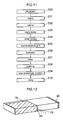
FIG. 1 is a perspective view of a laminated piezoelectric transformer according to first exemplary embodiment of the present invention,
FIG. 2 is an A-B sectional view of FIG. 1,
FIG. 3 is a C-D sectional view of FIG. 1,
FIG. 4 is an exploded perspective view of the laminated piezoelectric transformer shown in FIG. 1 before external electrodes are formed thereon,
FIG. 5 is a fabrication flowchart of the laminated piezoelectric transformer shown in FIG. 1,
FIG. 6 is a perspective view of a laminated piezoelectric transformer according to the second exemplary embodiment of the present invention,
FIG. 7 is a perspective view of a laminated piezoelectric transformer according to the third exemplary embodiment of the present invention,
FIG. 8 is an A-B sectional view of FIG. 7,
FIG. 9 is a C-D sectional view of FIG. 7,
FIG. 10 is an exploded perspective view of the laminated piezoelectric transformer shown in FIG. 7 before external electrodes are formed thereon,
FIG. 11 is a fabrication flowchart of the laminated piezoelectric transformer shown in FIG. 7,
FIG. 12 is a perspective view of a laminated piezoelectric transformer according to the fourth exemplary embodiment of the present invention,
FIG. 13 is a sectional view of a laminated piezoelectric transformer according to another exemplary embodiment of the present invention,
FIG. 14 is a sectional view of a laminated piezoelectric transformer according to still another exemplary embodiment of the present invention,
FIG. 15 is a enlarged sectional view of a main portion of a laminated piezoelectric transformer according to yet another exemplary embodiment of the present invention,
FIG. 16 is a sectional view of a laminated piezoelectric transformer according to another exemplary embodiment of the invention,
FIG. 17 is a enlarged sectional view of a main portion of a laminated piezoelectric transformer according to another exemplary embodiment of the present invention, and
FIG. 18 is a perspective view of a conventional laminated piezoelectric transformer.
DESCRIPTION OF THE PREFERRED EMBODIMENT
The laminated piezoelectric transformer of the present invention comprises:
a laminated body formed by laminating a plurality of ceramic layers and a plurality of internal electrodes; and
a plurality of external electrodes electrically connected to the internal electrodes and disposed on the surface of the laminated body. The internal electrodes are made up of a plurality of input side internal electrodes (hereinafter, called primary internal electrodes ) formed at the middle portion along the longitudinal direction of the laminated body and a plurality of output side internal electrodes (hereinafter, called secondary internal electrodes) formed at opposite end portions of the laminated body with respect to the longitudinal direction.
Another laminated piezoelectric transformer of the present invention is characterized by having a plurality of primary internal electrodes extending from the middle portion along the longitudinal direction of the laminated body to the vicinity of one end portion in the longitudinal direction of the same and a plurality of secondary internal electrodes disposed at another end portion of the laminated body.
Exemplary embodiments of the present invention will be described with reference to the accompanying drawings.
First Exemplary Embodiment
Fabrication processes of a laminated piezoelectric transformer shown in FIG. 1 will be described with reference to FIG. 2 to FIG. 5.
The laminated piezoelectric transformer according to the first exemplary embodiment of the invention comprises ceramic layer 1, primary internal electrodes 2 a, 2 b, secondary internal electrode 2 c, primary external electrode 3 a, and secondary external electrode 3 b. Processes for fabricating the same will be described in accordance with a fabrication flowchart shown in FIG. 5.
First, to produce the piezoelectric material of lead titanate zirconate system, PbO, ZrO2, TiO2 were used as the main raw materials and a predetermined proportion of sub raw materials were added thereto (100). The materials were then mixed in a ball mill for a predetermined period of time (101).
Then the mixed material powder were calcined (102), mixed with predetermined amounts of organic binder, plasticizer, and organic solvent, and were subjected to slurry mixing (103) to obtain slurry for forming sheets.
Then, sheet formation was carried out by coating the slurry with a doctor blade method (104) to obtain ceramic sheet 1 of a predetermined thickness.
Then, internal-electrode paste was printed on ceramic sheet 1 to form primary internal electrode 2 a, 2 b and secondary internal electrode 2 c of the shapes shown in FIG. 4 (105). The internal-electrode paste contains Ag—Pd as the main components and contains the raw material powders of the ceramic sheet, at least, as the sub components.
Then, a laminate of a required number of ceramic sheets having no internal-electrode paste printed thereon (hereinafter referred to as “ineffective layers”) was produced; ceramic sheets with internal-electrode paste printed thereon to provide desired characteristics were piled up thereon; and ineffective layers, again, were piled up thereon. Thus, a laminated body virtually of a rectangular parallelepiped shape was obtained (106).
At this time, as shown in FIG. 4, primary internal electrodes 2 a and 2 b are placed such that they are opposite to each other at the middle portion along the longitudinal direction of one layer of ceramic layer 1 and their edge portions are exposed on both side faces with respect to the transverse direction of the laminated body.
Further, secondary internal electrodes 2 c were formed at both end portions in the longitudinal direction of one layer of ceramic layer 1 such that they are exposed on both side faces in the transverse direction of the laminated body to be formed later.
Then, the organic binder within the laminated body was burned out to be removed and, thereafter, the laminated body was sintered one hour at the temperatures of 1000-1200° C. (107).
Then, the overall outer surface of the laminated body was polished such that end portions are given a curved shape and primary and secondary internal electrodes 2 a, 2 b, 2 b, 2 c are completely exposed on the outer surface of the laminated body.
Thereafter, primary external electrodes 3 a were formed on both side faces of the laminated body where internal electrodes 2 a, 2 b are exposed; and secondary external electrodes 3 b were formed on the end faces of the laminated body where internal electrodes 2 c are exposed (109).
Then, voltage was applied between the external electrodes 3 a to polarize ceramic layer 1 between internal electrodes 2 a and 2 b (hereinafter, ceramic layer 1 between internal electrodes 2 a and 2 b will be called “effective layer”). Thereafter, voltage is applied between external electrode 3 a used as the negative electrode and external electrode 3 b used as the positive electrode, so that the overall ceramic layers 1 between internal electrode 2 c and internal electrode 2 a, 2 b is polarized (110) and, thus, a laminated piezoelectric transformer was obtained.
Second Exemplary Embodiment
FIG. 6 is a perspective view of a laminated piezoelectric transformer according to the second exemplary embodiment. In the first exemplary embodiment, external electrode 3 a and external electrode 3 b were only formed on the side faces in the transverse direction of the laminated body. In the present exemplary embodiment, external electrode 3 a and external electrode 3 b are formed not only on the side face but also on the top and bottom faces of the laminated body.
By virtue of the configuration of the present exemplary embodiment, not only the adhesive strength between the laminated body and external electrodes 3 a, 3 b are increased but also the strength of the laminated body is increased.
Further, since outermost ceramic layers 1 constituting the top and bottom surfaces of the laminated body are also polarized by external electrodes 3 a, 3 b, the voltage step-up ratio is improved. In the interest of an improvement in the voltage step-up ratio, it is preferable that external electrodes 3 a, 3 b formed on the surface of the laminated body be as large as possible.
Third Exemplary Embodiment
Fabricating processes of a laminated piezoelectric transformer as shown in FIG. 7 will be described with reference to FIG. 8-FIG. 11. Parts corresponding to those in the first exemplary embodiment are denoted by the same reference numerals.
In the fabrication flowchart of FIG. 11, the steps down to the ceramic sheet formation are the same as in the first exemplary embodiment.
Then, internal-electrode paste was printed on the ceramic sheet to obtain primary and secondary internal electrodes 2 a, 2 b, 2 c (205) of the shapes as shown in FIG. 10. The internal-electrode paste contains Ag—Pd as the major components and the raw material powder of the ceramic sheet, at least, as the sub components.
Then, on a laminate of ineffective layers, ceramic sheets having the internal-electrode paste printed thereon were piled up such that desired characteristics are obtained. On the same, ineffective layers were piled up again to obtain a laminated body virtually in a rectangular parallelepiped shape (206).
At this time, primary internal electrodes 2 a, 2 b were disposed to extend from the middle portion along the longitudinal direction of one layer of ceramic layer 1 to its one end portion as shown in FIG. 10. Internal electrodes 2 a and 2 b were arranged to be opposite to each other with respect to the transverse direction and to have their end portions exposed on both side faces of the laminated body in the transverse direction. However, in order to prevent a short-circuit occurring between internal electrodes 2 a and 2 b, internal electrodes 2 a and 2 b were arranged not to expose on the end faces in the longitudinal direction.
It is because, if internal electrodes 2 a, 2 b on the input side are exposed on the end face in the longitudinal direction, there is a possibility of occurrence of migration between internal electrodes 2 a and 2 b by water or the like attaching thereto. Meanwhile, secondary internal electrode 2 c was formed at the other end portion in the longitudinal direction of one layer of ceramic layer 1 so as to expose on the side face in the transverse direction of the laminated body to be formed later.
Then, as was in the first exemplary embodiment, the laminated body was sintered (207) and overall external surface was subjected to polishing (208).
Then, primary external electrodes 3 a were formed on both side faces of the laminated body in the transverse direction where internal electrodes 2 a, 2 b are exposed. Further, secondary external electrode 3 b was formed on the side faces of the laminated body in the transverse direction where internal electrode 2 c is exposed (209).
Then, as was in the first exemplary embodiment, ceramic layer 1 between internal electrodes 3 a was polarized and the overall ceramic layer 1 was polarized (210) to obtain a laminated piezoelectric transformer.
Fourth Exemplary Embodiment
FIG. 12 is a perspective view of a laminated piezoelectric transformer according to the fourth exemplary embodiment. Although external electrode 3 a and external electrode 3 b, in the third exemplary embodiment, were formed only on the side face of the laminated body in the transverse direction, primary and secondary external electrodes 3 a, 3 b in the present exemplary embodiment are formed not only on the side faces of the laminated body but also on both top and bottom surfaces of the laminated body.
By virtue of the configuration described in the present embodiment, the adhesive strength between the laminated body and external electrodes 3 a, 3 b are increased and, also, the strength of the laminated body is increased.
Further, since the outermost ceramic layers 1 constituting the top and bottom faces of the laminated body in contact with external electrodes 3 a, 3 b are polarized, the voltage step-up ratio is improved. In the interest of an improvement in the voltage step-up ratio, it is preferable that external electrodes 3 a, 3 b on the input side and output side formed on the surface of the laminated body be as large as possible.
Preferred modes of carrying out the invention will be summarized below.
(1) As to the length of the laminated piezoelectric transformer in the transverse direction, it is preferred that the portion where internal electrodes 2 a, 2 b and internal electrode 2 c are not formed, i.e., the portion formed of only ceramic layer 1, be made shorter than the portion where internal electrodes 2 a, 2 b and internal electrode 2 c are formed, i.e., the portion in the middle and the portion at both ends of the laminated body.
By virtue of the configuration described, the electrostatic capacitance on the secondary side can be decreased. When a laminated piezoelectric transformer with a small electrostatic capacitance is incorporated into an inverter circuit, pulsations in the output voltage can be decreased and fluctuations in the cold cathode tube can be suppressed.
(2) Concerning the thickness of the laminated piezoelectric transformer, it is preferred that the portion where internal electrodes 2 a, 2 b, 2 c are not formed be made thinner than the portion where internal electrodes 2 a, 2 b, 2 c are formed as shown in FIG. 3 and FIG. 9. By virtue of this configuration, the electrostatic capacitance on the secondary side can be decreased.
(3) The laminated piezoelectric transformer can function as a laminated piezoelectric transformer even if it has no internal electrode 2 b formed therein. However, by forming internal electrode 2 b on the same plane with the internal electrode 2 a and connecting the same with the external electrode 3 a as in the above described exemplary embodiments, the total area of the internal electrodes can be enlarged so that the polarized volume of ceramic layer 1 on the secondary side is enlarged. Further, while the laminated body is pressed from top and bottom surfaces when the laminated body is fabricated, the laminated body can be pressed more uniformly by having internal electrode 2 b formed thereon.
(4) Although internal electrodes 2 a and 2 b were formed on the same plane in the exemplary embodiments described above, primary internal electrodes more than two may be formed.
For example, by dividing internal electrode 2 a in two at the middle portion of the laminated body with respect to the longitudinal direction as shown in FIG. 13, the strength at the middle portion of the laminated body, on which the maximum stress is loaded when the laminated piezoelectric transformer is driven, can be increased.
Further, for example, by dividing internal electrodes 2 a and 2 b in two at the middle portion of the laminated body along the longitudinal direction as shown in FIG. 14 so that four internal electrodes are formed on the same plane, the strength at the middle portion of the laminated body, on which the maximum stress is loaded when the laminated piezoelectric transformer is driven, can be increased.
In any case of division, it is preferred that the position at which the internal electrode is divided be the position of a node of oscillation.
(5) When the thickness of ceramic layer 1 is denoted by t and the distance between internal electrodes 2 a and 2 b on the same plane is denoted by x, occurrence of a dielectric breakdown can be prevented by setting t/4<X.
(6) At least part of the edge portions of internal electrodes 2 a, 2 b, and 2 c are arranged not to confront each other through ceramic layer 1 in the direction of the thickness of the laminated body as shown in FIG. 3. (More specifically, the sizes of internal electrodes 2 a, 2 b, 2 c are varied from layer to layer; or, even when they are formed in the same shape, positions at which they are disposed on ceramic layer 1 are shifted.) By virtue of this arrangement, concentration of polarization distortions at the edge portions of internal electrodes 2 a, 2 b, 2 c can be suppressed. The concentration of polarization distortions can be suppressed more strongly according as the portion where the confrontation through ceramic layer 1 is absent is made larger.
(7) By providing external electrodes 3 a and 3 b on the same side face of the laminated body in the transverse direction, inhibition of oscillation by the electrodes can be suppressed so that energy conversion efficiency is enhanced. By virtue of this configuration, external electrodes 3 a and 3 b can be formed at the same time and, therefore, the fabrication process of the external electrodes can be shortened.
(8) By roughening the surface of internal electrodes 2 a, 2 b, 2 c to a surface roughness of around several μm, the adhesive strength between ceramic layer 1 and internal electrodes 2 a, 2 b, 2 c can be increased.
One of the methods to roughen the surface of the internal electrode is to mix the raw material powder for forming the ceramic layer into the internal-electrode paste for forming the internal electrode. Preferable amount of the admixture is 10-100% by weight in 100% by weight of the metallic content of the internal-electrode paste.
By the arrangement described, adjoining ceramic layers 1 positioned between the internal electrodes can be sintered together so that the adhesive strength can further be increased.
(9) By making the average particle size of the ceramic material larger than the average particle size of the metallic components in the internal electrode, the adhesive strength between the ceramic layer and the internal electrode can be increased.
(10) By forming the surfaces at the end portions of the piezoelectric laminated body into a curved shape, stress concentration on the end portions of the laminated body can be suppressed so that the rupture strength of the same can be increased and the breakdown electric power during its operation can be improved.
(11) By forming at least part of the circumferential portion of the internal electrode into a curved shape as shown in FIG. 15, occurrence of concentration of polarization strain on circumferential portions of internal electrodes 2 a, 2 b, 2 c can be suppressed and the withstand electric power during operation can be improved.
(12) By making the average grain size of the ceramic layer having no internal electrodes formed thereon larger than the average grain size of the ceramic layer between internal electrodes, polarization strains can be relaxed and strength increased.
(13) By making the thickness of the ineffective layer equal to or smaller than the thickness of the effective layer, it becomes possible to protect the laminated body, which vibrates while it is driven, without greatly decreasing the voltage step-up ratio and conversion efficiency.
(14) It is preferred to make the angles between each of adjoining sides of the laminated body non-rectangular, i.e., to form the cross-section of the laminated body with respect to the transverse direction virtually into a trapezoidal shape. By virtue of this arrangement, when, for example, a laminated piezoelectric transformer is incorporated into case 200 as shown in FIG. 16, the laminated piezoelectric transformer is securely fixed in place and securely put into electrical connection with electrodes (not shown) provided on case 200 by means of electrically conductive rubber 201. At this time, it is preferred that the longer side of the laminated piezoelectric transformer be placed on the bottom side of case 200.
Further, the piezoelectric transformer can securely maintain its electrical connection with electrodes on case 200 even when subjected to vibration or shock.
(15) In the present invention, it is arranged such that the length of internal electrode 2 a, 2 b, 2 c exposed on the side face of the laminated body is larger than the width of external electrode 3 a, 3 b as shown in FIGS. 1, 6, 7 and 12. By virtue of this arrangement, concentration of electric field on the edge portion of external electrode 3 a, 3 b leading to deterioration in the characteristics can be prevented.
By making internal electrode 2 a at the end portions thinner than that at the middle portion as shown in FIG. 17, the adhesive strength at the interface between end portions of internal electrode 2 a and ceramic layer 1 can be increased. Of course, this can also be said of other internal electrodes 2 b, 2 c.
(16) In the laminated piezoelectric transformers of the configuration as shown in exemplary embodiments 3 and 4, the length of internal electrodes 2 a, 2 b in the longitudinal direction of the laminated body is made greater than half the length of the laminated body in the longitudinal direction. This arrangement is made for preventing the border of polarization from overlapping with the portion on which the maximum stress is placed. In other words, it is preferred that edge portions of internal electrodes 2 a, 2 b do not overlap with the node of oscillation.
INDUSTRIAL APPLICABILITY
According to the present invention, as described above, a laminated piezoelectric transformer capable of stepping up voltage at high energy conversion efficiency can be provided. Accordingly, by the use of the laminated piezoelectric transformer of the invention, power consumption in electronic devices can be decreased.