WO2019229873A1 - 活性ガス生成装置 - Google Patents
活性ガス生成装置 Download PDFInfo
- Publication number
- WO2019229873A1 WO2019229873A1 PCT/JP2018/020736 JP2018020736W WO2019229873A1 WO 2019229873 A1 WO2019229873 A1 WO 2019229873A1 JP 2018020736 W JP2018020736 W JP 2018020736W WO 2019229873 A1 WO2019229873 A1 WO 2019229873A1
- Authority
- WO
- WIPO (PCT)
- Prior art keywords
- electrode
- active gas
- dielectric
- gas
- conductive film
- Prior art date
Links
- 239000002184 metal Substances 0.000 claims abstract description 90
- 239000007789 gas Substances 0.000 claims description 260
- IJGRMHOSHXDMSA-UHFFFAOYSA-N Atomic nitrogen Chemical compound N#N IJGRMHOSHXDMSA-UHFFFAOYSA-N 0.000 claims description 14
- 230000003213 activating effect Effects 0.000 claims description 6
- 239000000470 constituent Substances 0.000 claims description 6
- 229910052594 sapphire Inorganic materials 0.000 claims description 5
- 239000010980 sapphire Substances 0.000 claims description 5
- KZBUYRJDOAKODT-UHFFFAOYSA-N Chlorine Chemical compound ClCl KZBUYRJDOAKODT-UHFFFAOYSA-N 0.000 claims description 4
- 239000000919 ceramic Substances 0.000 claims description 4
- 239000011521 glass Substances 0.000 claims description 4
- 239000000463 material Substances 0.000 claims description 4
- 229910052757 nitrogen Inorganic materials 0.000 claims description 4
- PXGOKWXKJXAPGV-UHFFFAOYSA-N Fluorine Chemical compound FF PXGOKWXKJXAPGV-UHFFFAOYSA-N 0.000 claims description 3
- QVGXLLKOCUKJST-UHFFFAOYSA-N atomic oxygen Chemical compound [O] QVGXLLKOCUKJST-UHFFFAOYSA-N 0.000 claims description 3
- 239000011737 fluorine Substances 0.000 claims description 3
- 229910052731 fluorine Inorganic materials 0.000 claims description 3
- 239000001257 hydrogen Substances 0.000 claims description 3
- 229910052739 hydrogen Inorganic materials 0.000 claims description 3
- 239000001301 oxygen Substances 0.000 claims description 3
- 229910052760 oxygen Inorganic materials 0.000 claims description 3
- 125000004435 hydrogen atom Chemical class [H]* 0.000 claims 1
- 230000005684 electric field Effects 0.000 abstract description 24
- 230000009467 reduction Effects 0.000 abstract description 2
- 238000002347 injection Methods 0.000 abstract 1
- 239000007924 injection Substances 0.000 abstract 1
- QJGQUHMNIGDVPM-UHFFFAOYSA-N nitrogen(.) Chemical compound [N] QJGQUHMNIGDVPM-UHFFFAOYSA-N 0.000 description 30
- 238000000034 method Methods 0.000 description 15
- 230000004888 barrier function Effects 0.000 description 13
- 238000004088 simulation Methods 0.000 description 13
- 230000002159 abnormal effect Effects 0.000 description 9
- 230000015572 biosynthetic process Effects 0.000 description 9
- 230000000694 effects Effects 0.000 description 8
- 230000004048 modification Effects 0.000 description 7
- 238000012986 modification Methods 0.000 description 7
- 238000010586 diagram Methods 0.000 description 6
- 229910001873 dinitrogen Inorganic materials 0.000 description 6
- 238000004519 manufacturing process Methods 0.000 description 6
- 239000011148 porous material Substances 0.000 description 6
- 239000002994 raw material Substances 0.000 description 4
- 230000002093 peripheral effect Effects 0.000 description 3
- UFHFLCQGNIYNRP-UHFFFAOYSA-N Hydrogen Chemical compound [H][H] UFHFLCQGNIYNRP-UHFFFAOYSA-N 0.000 description 2
- 230000015556 catabolic process Effects 0.000 description 2
- 238000004140 cleaning Methods 0.000 description 2
- 238000011109 contamination Methods 0.000 description 2
- 238000005260 corrosion Methods 0.000 description 2
- 230000007797 corrosion Effects 0.000 description 2
- 238000005530 etching Methods 0.000 description 2
- 238000011156 evaluation Methods 0.000 description 2
- 238000010304 firing Methods 0.000 description 2
- 150000004767 nitrides Chemical class 0.000 description 2
- 238000005121 nitriding Methods 0.000 description 2
- 150000002831 nitrogen free-radicals Chemical class 0.000 description 2
- 238000004544 sputter deposition Methods 0.000 description 2
- 239000000758 substrate Substances 0.000 description 2
- 239000013078 crystal Substances 0.000 description 1
- 230000009849 deactivation Effects 0.000 description 1
- 239000003989 dielectric material Substances 0.000 description 1
- 150000002221 fluorine Chemical class 0.000 description 1
- 150000002431 hydrogen Chemical class 0.000 description 1
- 239000012212 insulator Substances 0.000 description 1
- 150000002500 ions Chemical class 0.000 description 1
- 230000008569 process Effects 0.000 description 1
- 230000001902 propagating effect Effects 0.000 description 1
- 230000009291 secondary effect Effects 0.000 description 1
- 238000004904 shortening Methods 0.000 description 1
- 239000007787 solid Substances 0.000 description 1
- 125000006850 spacer group Chemical group 0.000 description 1
Images


Classifications
-
- H—ELECTRICITY
- H01—ELECTRIC ELEMENTS
- H01J—ELECTRIC DISCHARGE TUBES OR DISCHARGE LAMPS
- H01J37/00—Discharge tubes with provision for introducing objects or material to be exposed to the discharge, e.g. for the purpose of examination or processing thereof
- H01J37/32—Gas-filled discharge tubes
- H01J37/32009—Arrangements for generation of plasma specially adapted for examination or treatment of objects, e.g. plasma sources
- H01J37/32357—Generation remote from the workpiece, e.g. down-stream
-
- B—PERFORMING OPERATIONS; TRANSPORTING
- B01—PHYSICAL OR CHEMICAL PROCESSES OR APPARATUS IN GENERAL
- B01J—CHEMICAL OR PHYSICAL PROCESSES, e.g. CATALYSIS OR COLLOID CHEMISTRY; THEIR RELEVANT APPARATUS
- B01J19/00—Chemical, physical or physico-chemical processes in general; Their relevant apparatus
- B01J19/08—Processes employing the direct application of electric or wave energy, or particle radiation; Apparatus therefor
-
- H—ELECTRICITY
- H01—ELECTRIC ELEMENTS
- H01J—ELECTRIC DISCHARGE TUBES OR DISCHARGE LAMPS
- H01J37/00—Discharge tubes with provision for introducing objects or material to be exposed to the discharge, e.g. for the purpose of examination or processing thereof
- H01J37/32—Gas-filled discharge tubes
- H01J37/32009—Arrangements for generation of plasma specially adapted for examination or treatment of objects, e.g. plasma sources
- H01J37/32348—Dielectric barrier discharge
-
- H—ELECTRICITY
- H01—ELECTRIC ELEMENTS
- H01J—ELECTRIC DISCHARGE TUBES OR DISCHARGE LAMPS
- H01J37/00—Discharge tubes with provision for introducing objects or material to be exposed to the discharge, e.g. for the purpose of examination or processing thereof
- H01J37/32—Gas-filled discharge tubes
- H01J37/32431—Constructional details of the reactor
- H01J37/3244—Gas supply means
-
- H—ELECTRICITY
- H01—ELECTRIC ELEMENTS
- H01J—ELECTRIC DISCHARGE TUBES OR DISCHARGE LAMPS
- H01J37/00—Discharge tubes with provision for introducing objects or material to be exposed to the discharge, e.g. for the purpose of examination or processing thereof
- H01J37/32—Gas-filled discharge tubes
- H01J37/32431—Constructional details of the reactor
- H01J37/32532—Electrodes
- H01J37/32541—Shape
-
- H—ELECTRICITY
- H01—ELECTRIC ELEMENTS
- H01J—ELECTRIC DISCHARGE TUBES OR DISCHARGE LAMPS
- H01J37/00—Discharge tubes with provision for introducing objects or material to be exposed to the discharge, e.g. for the purpose of examination or processing thereof
- H01J37/32—Gas-filled discharge tubes
- H01J37/32431—Constructional details of the reactor
- H01J37/32532—Electrodes
- H01J37/3255—Material
-
- H—ELECTRICITY
- H01—ELECTRIC ELEMENTS
- H01J—ELECTRIC DISCHARGE TUBES OR DISCHARGE LAMPS
- H01J2237/00—Discharge tubes exposing object to beam, e.g. for analysis treatment, etching, imaging
- H01J2237/32—Processing objects by plasma generation
- H01J2237/327—Arrangements for generating the plasma
Definitions
- the present invention relates to an active gas generator that generates an active gas by a parallel plate type dielectric barrier discharge and supplies the active gas to a subsequent processing space.
- Patent Document 1 An active gas generating device that generates an active gas by a parallel plate type dielectric barrier discharge is disclosed in, for example, Patent Document 1.
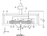
- FIG. 14 is a diagram showing a schematic configuration of a conventional nitrogen radical generation system 100 disclosed in Patent Document 1.
- the nitrogen radical generation system 100 includes a nitrogen radical generation device 101, an AC voltage source 108, and a processing chamber 112.
- the nitrogen radical generator 101 which is an active gas generator, generates nitrogen radicals, which are active gases, from nitrogen gas using dielectric barrier discharge.
- a discharge unit for generating a dielectric barrier discharge is disposed in the space 102 in the nitrogen radical generator 101.
- the discharge unit includes a first electrode 103 and a second electrode 104.
- the second electrode 104 is installed at the center of the bottom surface of the nitrogen radical generator 101.
- the first electrode 103 is disposed so as to face the second electrode 104.
- the first electrode 103 and the second electrode 104 face each other with a predetermined distance. That is, a discharge space 105 is formed between the first electrode 103 and the second electrode 104.
- a dielectric (not shown in FIG. 14) is disposed on at least one of the main surface of the first electrode 103 facing the discharge space 105 and the main surface of the second electrode 104 facing the discharge space 105. It is installed.
- the discharge unit can generate a dielectric barrier discharge in the discharge space 105 between the first electrode 103 and the second electrode 104.
- a gas supply port 106 is disposed at the center of the upper surface of the nitrogen radical generator 101. Nitrogen gas, which is a raw material gas, is supplied from the outside of the nitrogen radical generator 101 to the space 102 in the nitrogen radical generator 101 through the gas supply port 106.
- one gas discharge portion 107 through which nitrogen radical gas is output to the outside of the nitrogen radical generator 101 is formed.
- AC voltage source 108 applies a high-voltage AC voltage to the discharge unit.
- One terminal of the AC voltage source 108 is electrically connected to the first electrode 103.
- the other terminal of the AC voltage source 108 is electrically connected to the casing (ground) of the nitrogen radical generator 101.
- the second electrode 104 is disposed on the bottom surface of the nitrogen radical generator 101. Therefore, the other terminal of the AC voltage source 108 is electrically connected to the second electrode 104 via the nitrogen radical generator 101.
- the AC voltage source 108 applies a high-voltage AC voltage between the first electrode 103 and the second electrode 104.
- a dielectric barrier discharge is generated in the discharge space 105 between the first electrode 103 and the second electrode 104 by application of the AC voltage.
- the nitrogen gas supplied from the gas supply port 106 enters the discharge space 105 from the outer periphery of each electrode 103,104. Then, the nitrogen gas propagates from the outer peripheral portion of each electrode 103, 104 to the inside. Due to the dielectric barrier discharge generated in the discharge space 105, nitrogen radical gas is generated from the propagating nitrogen gas. The generated nitrogen radical gas is output from the gas discharge unit 107 to the outside of the nitrogen radical generator 101.
- a processing chamber 112 is disposed below the nitrogen radical generator 101.
- the bottom surface of the nitrogen radical generator 101 and the top surface of the processing chamber 112 are in contact with each other.
- an orifice unit 109 is disposed between the nitrogen radical generator 101 and the processing chamber 112.
- the orifice unit 109 connects the gas discharge unit 107 and the processing chamber 111 in the processing chamber 112 through the pores 110.
- the diameter of the pore 110 of the orifice portion 109 is smaller than the diameter of the hole of the gas discharge portion 107. More specifically, the diameter of the inlet of the pore 110 of the orifice portion 109 is smaller than the diameter of the outlet of the hole of the gas discharge portion 107. Therefore, a pressure section between the space 102 in the nitrogen radical generating apparatus 101 and the processing chamber 111 is formed by the pores 110 of the orifice portion 109.
- processing using nitrogen radicals generated by the nitrogen radical generating device 101 and output from the nitrogen radical generating device 101 is performed. .
- a susceptor 114 is disposed in a processing chamber 111 in the processing chamber 112, and a wafer (substrate) 113 that is a processing target is placed on the susceptor 114.
- a gas exhaust unit 115 is disposed on the side surface of the processing chamber 112.
- the pressure in the processing chamber 111 is maintained constant by the gas exhaust unit 115, for example, in the range of about 1 Torr to 100 Torr.
- the gas exhaust processing by the gas exhaust unit 115 generates not only the pressure setting of the space 102 and the processing chamber 111 but also the flow of nitrogen gas and nitrogen radical gas from the nitrogen radical generating apparatus 101 to the processing chamber 112. .
- the nitrogen radical generating apparatus 101 in the conventional nitrogen radical generating system 100 shown in FIG. 14 generates a dielectric barrier discharge in the discharge space 105 between the first electrode 103 and the second electrode 104, and generates a dielectric.
- the active gas obtained by the body barrier discharge is supplied to the processing chamber 111 as a subsequent apparatus via the gas discharge part 107 and the pores 110 of the orifice part 109.
- the voltage applied to generate the dielectric barrier discharge generates a region having an electric field strength that causes dielectric breakdown also in the processing chamber 111 of the processing chamber 112 which is a subsequent apparatus.
- An abnormal discharge which is a discharge that causes contamination, is generated.
- the processing chamber 111 is under a reduced pressure environment as compared with the space 102 in the nitrogen radical generating apparatus 101, ions generated by abnormal discharge are accelerated by the electric field and collide with the wafer 113, causing damage to the wafer 113. was there.
- a sufficient distance between a portion to which a high voltage is applied such as the first electrode 103 (hereinafter may be referred to as a “voltage application unit”) and a subsequent apparatus (processing chamber 112) is sufficient. As much as it can be taken, the electric field strength in the latter apparatus can be reduced.
- a second method for lowering the voltage value of the AC voltage supplied from the AC voltage source 108 can be considered. However, if the second method is adopted, the amount of generated active gas is reduced, which is not desirable.
- the first and second methods described above have problems that are not desirable methods for suppressing abnormal discharge.
- an active gas generation device that solves the above-described problems and can intentionally weaken the electric field strength of the processing space provided below the orifice portion without changing the structure of the orifice portion.
- the purpose is to provide.
- the active gas generation device is an active gas generation device that generates an active gas obtained by activating a source gas supplied to a discharge space, and includes a first electrode component and the first electrode component. A first electrode electrode formed on the upper surface of the first dielectric electrode and the first dielectric electrode. And the second electrode component includes a second dielectric electrode and a second metal electrode formed on a lower surface of the second dielectric electrode, and the first and second An area where the first and second metal electrodes overlap in plan view in the dielectric space where an AC voltage is applied between the two metal electrodes and the first and second dielectric electrodes face each other is the discharge space. And the second dielectric electrode is a small electrode for ejecting the active gas to the outside.
- a path from the discharge space to the at least one gas ejection hole is defined as an active gas flow path having at least one gas ejection hole
- the active gas generator includes the second dielectric electrode itself or An orifice part provided below the second dielectric electrode and having at least one through hole corresponding to the at least one gas ejection hole, wherein the first electrode component part comprises the first dielectric member.
- An auxiliary conductive film formed on the upper surface of the body electrode independently of the first metal electrode, and the auxiliary conductive film is provided so as to overlap a part of the active gas flow path in plan view; In addition, the auxiliary conductive film is set to a ground potential.
- the active gas generation apparatus according to the present invention according to claim 1 has the above characteristics, so that the electric field strength in the active gas flow path can be reduced by the auxiliary conductive film set to the ground potential.
- the present invention according to claim 1 has the main effect that the electric field strength of the processing space provided below the orifice part can be intentionally reduced without changing the structure of the orifice part.
- FIG. 1 is an explanatory view showing a basic configuration of an active gas generation apparatus according to an embodiment of the present invention.
- FIG. 1 shows an XYZ orthogonal coordinate system.
- the active gas generation device 51 of the present embodiment is an active gas generation device that generates an active gas 7 obtained by activating the raw material gas 6 supplied to the discharge space 15.
- the active gas generation device 51 includes a metal casing 31, a gas supply port 32, an active gas generation electrode group 301, and an orifice portion 40 as main components.
- the metal casing 31 is a casing for the metal active gas generation device 51 set to the ground potential.
- the gas supply port 32 is attached to the upper portion, and the source gas 6 is supplied from the gas supply port 32 to the metal casing 31. Is supplied to the internal space 33.
- the active gas generating electrode group 301 is disposed in the internal space 33 of the metal casing 31 in the active gas generating device 51. Specifically, the active gas generating electrode group 301 is disposed on the bottom surface of the metal casing 31. The orifice portion 40 is incorporated in a part of the bottom surface of the metal casing 31.
- the active gas generation electrode group 301 includes a combination of a high-voltage side electrode configuration unit 1 that is a first electrode configuration unit and a ground-side electrode configuration unit 2 that is a second electrode configuration unit.
- the component 2 is provided below the high-voltage side electrode component 1.
- the high-voltage side electrode configuration unit 1 includes a dielectric electrode 11 as a first dielectric electrode and a metal electrode 10 as a first metal electrode formed on the upper surface of the dielectric electrode 11 as main components. Have.
- the high-voltage side electrode configuration unit 1 further includes a conductive film 12 that is an auxiliary conductive film formed independently of the metal electrode 10 on the upper surface of the dielectric electrode 11.
- the metal conductive film 12 is provided between at least one gas ejection hole 9 and the metal metal electrode 10 in plan view.
- the metal conductive film 12 may overlap with at least one gas ejection hole 9 in plan view.
- the metal electrode 10 and the conductive film 12 are provided on the upper surface of the dielectric electrode 11 by using, for example, a sputtering method or a printing firing method.
- the ground-side electrode constituting unit 2 includes a dielectric electrode 21 that is a second dielectric electrode and a metal electrode 20 that is a second metal electrode formed on the lower surface of the dielectric electrode 21 as main components. ing.
- the metal electrode 20 is provided on the lower surface of the dielectric electrode 21 using a sputtering method, a printing firing method, or the like.
- the dielectric electrode 11 of the high-voltage side electrode constituting unit 1 and the dielectric electrode 21 of the ground side electrode constituting unit 2 are installed so as to be provided with a predetermined constant interval by a spacer or the like (not shown).
- an AC voltage is applied from the high frequency power source 5 between the metal electrode 10 and the metal electrode 20.
- an AC voltage is applied to the metal electrode 10 from the high frequency power supply 5, and the metal electrode 20 and the conductive film 12 are set to the ground potential via the metal housing 31.
- a discharge space 15 is provided including a region where the metal electrodes 10 and 20 overlap in plan view.
- the shape of the upper surface of the dielectric electrode 11 and the shape of the lower surface of the dielectric electrode 21 may be the same, or a predetermined shape may be provided. For example, on the upper surface of the dielectric electrode 11, an uneven shape that becomes an obstacle may be provided so that creeping discharge does not occur between the metal electrode 10 and the conductive film 12.
- the dielectric electrode 21 has at least one gas ejection hole 9 for ejecting the active gas 7 to the external processing space 63.
- the orifice part 40 is provided below the dielectric electrode 21 and has at least one through hole 49 corresponding to the at least one gas ejection hole 9.
- the orifice portion 40 is made of one of ceramic, glass, and sapphire.
- an AC voltage is applied between the metal electrodes 10 and 20 to generate a dielectric barrier discharge in the discharge space 15 of the active gas generating electrode group 301, and at the same time, the gas supply port 32.
- the raw material gas 6 is supplied into the internal space 33 of the metal casing 31 from the outer peripheral portion of the active gas generating electrode group 301 to the inside.
- the active gas 7 is generated by activating the source gas 6 in the discharge space 15, and the generated active gas 7 is at least from the discharge space 15 in the dielectric space. It flows through an active gas flow path that is a path to one gas ejection hole 9.
- the active gas 7 flowing through the active gas flow path is finally supplied to the subsequent processing space 63 along the gas flow 18 via the at least one gas ejection hole 9 and the through hole 49 of the orifice portion 40.
- the conductive film 12 is provided so as to overlap a part of the active gas flow path in plan view.
- the active gas generation device 51 of the present embodiment has the following features (1) and (2).
- the conductive film 12 is provided so as to overlap a part of the active gas flow path in plan view. (2) The conductive film 12 is set to the ground potential.
- a first mode and a second mode described below are conceivable as specific configurations for realizing the basic configuration of the active gas generator 51 of the embodiment shown in FIG.
- FIGS. 2 to 5 are views showing the structure of the active gas generating electrode group 301A of the first mode in the active gas generating apparatus 51 of the first embodiment.
- the XYZ orthogonal coordinate system is shown in each of FIGS.
- the first mode of the active gas generation apparatus 51 employs the active gas generation electrode group 301A shown in FIGS. 2 to 5 as the active gas generation electrode group 301 having the basic configuration shown in FIG.
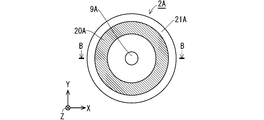
- FIG. 2 is a plan view of the high-voltage side electrode constituting portion 1A according to the first aspect as viewed from above (+ Z direction side).
- FIG. 3 is a plan view of the ground-side electrode constituting portion 2A according to the first aspect as viewed from below ( ⁇ Z direction side).
- FIG. 4 is a sectional view showing a sectional structure in the XZ plane of the active gas generating electrode group 301A.
- FIG. 5 is an explanatory diagram schematically showing the overall configuration of the active gas generation electrode group 301A.
- the active gas generation electrode group 301A according to the first embodiment will be described with reference to FIGS. 2 to 5 as appropriate.
- the active gas generation electrode group 301A includes a high-voltage side electrode configuration unit 1A that is a first electrode configuration unit and a ground-side electrode configuration unit 2A that is a second electrode configuration unit. It is comprised by combination.
- the ground side electrode configuration part 2A is provided below the high voltage side electrode configuration part 1A.
- the active gas generation electrode group 301A employs a parallel plate method.
- the high-voltage-side electrode constituting unit 1A includes a dielectric electrode 11A that is a first dielectric electrode and a metal electrode 10A that is a first metal electrode formed on the upper surface of the dielectric electrode 11A as main components. Have.
- the high-voltage-side electrode component 1A further includes a conductive film 12A that is an auxiliary conductive film formed independently of the metal electrode 10A on the upper surface of the dielectric electrode 11A.
- the dielectric electrode 11A is formed in a circular shape in plan view
- the metal electrode 10A is formed in an annular shape in plan view
- the conductive film 12A is formed in a circular shape in plan view.
- the conductive film 12A is disposed on the center of the dielectric electrode 11A so as to overlap the gas ejection hole 9A in plan view.
- the metal electrode 10 ⁇ / b> A is disposed at a predetermined distance from the outer periphery of the conductive film 12 so as to surround the conductive film 12. 2 is the cross-sectional structure of FIG.
- the ground-side electrode constituent part 2A has as main constituent parts a dielectric electrode 21A that is a second dielectric electrode and a metal electrode 20A that is a second metal electrode formed on the lower surface of the dielectric electrode 21A.
- a dielectric electrode 21A that is a second dielectric electrode
- a metal electrode 20A that is a second metal electrode formed on the lower surface of the dielectric electrode 21A.
- the dielectric electrode 11A has a single gas ejection hole 9A for ejecting the active gas 7 to the external processing space 63.
- the single gas ejection hole 9A corresponds to at least one gas ejection hole 9 in the basic configuration shown in FIG.
- the dielectric electrode 21A is formed in a circular shape in plan view
- the metal electrode 12A is formed in an annular shape in plan view
- the single gas ejection hole 9A is circular in a plan view. Formed.
- the gas ejection hole 9A is provided at the center of the dielectric electrode 21A in plan view.
- the metal electrode 20A is disposed at a predetermined distance from the outer periphery of the gas ejection hole 9A so as to surround the periphery of the gas ejection hole 9A.
- the BB cross section of FIG. 3 is the cross sectional structure of FIG.
- a path from the discharge space 15 to the single gas ejection hole 9A in the dielectric space formed between the dielectric electrodes 11A and 21A is an active gas flow path.
- the conductive film 12A is disposed at a position overlapping the gas ejection hole 9A in plan view. That is, the conductive film 12A is disposed so as to be planar and overlap with a part of the active gas flow path.
- an AC voltage is applied from the high frequency power source 5 between the metal electrode 10A and the metal electrode 20A.
- an AC voltage is applied to the metal electrode 10 ⁇ / b> A from the high frequency power supply 5, and the metal electrode 20 ⁇ / b> A and the conductive film 12 ⁇ / b> A are set to the ground potential via the metal housing 31.
- the orifice portion 40 of the first aspect is provided below the dielectric electrode 21A and has a single through hole 49 corresponding to the single gas ejection hole 9A.
- the conductive film 12A is provided so as to overlap a part of the active gas flow path in plan view, and the conductive film 12A is set to the ground potential. It is characterized by being. That is, the first aspect has the above-described features (1) and (2) of the basic configuration.
- the first mode of the active gas generating device 51 having such a configuration, an AC voltage is applied between the metal electrodes 10A and 20A to generate a dielectric barrier discharge in the discharge space 15 of the active gas generating electrode group 301A. Further, the first mode of the active gas generation device 51 is configured to supply the source gas 6 from the gas supply port 32 into the internal space 33 of the metal casing 31 and to supply a single gas from the outer periphery of the active gas generation electrode group 301A. The source gas 6 is circulated with the direction toward the gas ejection hole 9A as the gas flow 8 (see FIG. 5).
- the active gas 7 is generated by activating the source gas 6 in the discharge space 15, and the generated active gas 7 is generated in the dielectric space. It flows through an active gas flow path that is a path from the discharge space 15 to the single gas ejection hole 9A.
- the active gas 7 flowing through the active gas flow path is finally supplied to the processing space 63 in the subsequent stage along the gas flow 18 via the single gas ejection hole 9 and the through hole 49 of the orifice portion 40.
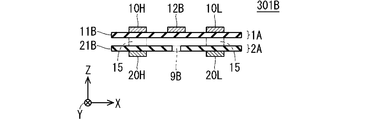
- FIGS. 6 to 9 are views showing the structure of the active gas generating electrode group 301B of the second mode in the active gas generating apparatus 51 of the embodiment.
- Each of FIGS. 6 to 9 shows an XYZ orthogonal coordinate system.
- the second mode of the active gas generation apparatus 51 employs the active gas generation electrode group 301B shown in FIGS. 6 to 9 as the active gas generation electrode group 301 having the basic configuration shown in FIG.
- FIG. 6 is a plan view of the high-voltage side electrode constituting portion 1B according to the second aspect as viewed from above (+ Z direction side).
- FIG. 7 is a plan view of the ground-side electrode constituting portion 2B according to the second aspect as viewed from below ( ⁇ Z direction side).
- FIG. 8 is a cross-sectional view showing a cross-sectional structure in the XZ plane of the active gas generating electrode group 301B.
- FIG. 9 is an explanatory diagram schematically showing the overall configuration of the active gas generation electrode group 301B.
- the active gas generation electrode group 301B of the second aspect will be described with reference to FIGS. 6 to 9 as appropriate.
- the active gas generation electrode group 301B includes a high-voltage side electrode configuration unit 1B that is a first electrode configuration unit and a ground-side electrode configuration unit 2B that is a second electrode configuration unit. It is comprised by combination.
- the ground side electrode configuration part 2B is provided below the high voltage side electrode configuration part 1B.
- the active gas generation electrode group 301B employs a parallel plate method.
- the high-voltage side electrode constituting unit 1B mainly includes a dielectric electrode 11B that is a first dielectric electrode, and metal electrode pairs 10H and 10L that are first metal electrodes formed on the upper surface of the dielectric electrode 11B. It has as a component.
- the high-voltage side electrode constituting unit 1B further includes a conductive film 12B that is an auxiliary conductive film formed independently of the metal electrode pairs 10H and 10L on the upper surface of the dielectric electrode 11B.
- the dielectric electrode 11B is formed in a rectangular shape with the Y direction as the long side direction when viewed in plan, and the metal electrode pairs 10H and 10L each have the Y direction as the long side direction when viewed in plan.
- the conductive film 12B is formed in a rectangular shape with the Y direction as the long side direction when seen in a plan view.
- the conductive film 12B is disposed on the center portion in the X direction of the dielectric electrode 11B in plan view.
- the metal electrode pairs 10H and 10L are arranged at a predetermined distance from the conductive film 12B so as to sandwich the conductive film 12B. That is, the metal electrode 10H is disposed on the left side ( ⁇ X direction side) with respect to the conductive film 12B, and the metal electrode 10L is disposed on the right side (+ X direction side) with respect to the conductive film 12B.
- 6 is the cross-sectional structure of FIG.
- the ground-side electrode constituting unit 2B mainly includes a dielectric electrode 21B as a second dielectric electrode and metal electrode pairs 20H and 20L as second metal electrodes formed on the lower surface of the dielectric electrode 21B. It has as a component.
- the dielectric electrode 11B has a plurality of gas ejection holes 9B for ejecting the active gas 7 to the external processing space 63.
- the plurality of gas ejection holes 9B correspond to at least one gas ejection hole 9 in the basic configuration shown in FIG.
- the dielectric electrode 21B is formed in a rectangular shape with the Y direction as the long side direction when viewed in plan, and the metal electrode pairs 20H and 20L each have the Y direction as the long side direction when viewed in plan.
- the plurality of gas ejection holes 9B are formed in a circular shape in plan view.
- the plurality of gas ejection holes 9B are discretely provided along the Y direction and provided in the dielectric electrode 21B. Each of the plurality of gas ejection holes 9B is disposed at the center position in the X direction of the dielectric electrode 21B.
- the metal electrode pairs 20H and 20L are arranged at a predetermined distance so as to sandwich the plurality of gas ejection holes 9B.
- the metal electrode 20H is disposed on the left side ( ⁇ X direction side) with respect to the plurality of gas ejection holes 9B, and the metal electrode 20L is disposed on the right side (+ X direction side) with respect to the plurality of gas ejection holes 9B.
- the DD cross section of FIG. 7 is the cross sectional structure of FIG.
- the path from the discharge space 15 to the plurality of gas ejection holes 9A in the dielectric space formed between the dielectric electrodes 11B and 21B is the active gas flow path.
- the conductive film 12B is arranged at a position overlapping the plurality of gas ejection holes 9B in plan view. That is, the conductive film 12B is disposed so as to be planar and overlap with a part of the active gas flow path.
- an AC voltage is applied from the high frequency power source 5 between the metal electrode pair 10H and 10L and the metal electrode pair 20H and 20L. Specifically, an AC voltage is applied to the metal electrode pairs 10H and 10L from the high-frequency power source 5, and the metal electrode pairs 20H and 20L and the conductive film 12B are set to the ground potential via the metal casing 31.
- the orifice section 40 of the second aspect is provided below the dielectric electrode 21B and has a plurality of through holes 49 corresponding to the plurality of gas ejection holes 9B.
- the conductive film 12B is provided so as to overlap a part of the active gas flow path in plan view, and the conductive film 12B is set to the ground potential. It is characterized by being. That is, the second aspect has the above-mentioned features (1) and (2) of the basic configuration.
- the second mode of the active gas generation device 51 having such a configuration, an alternating voltage is applied between the metal electrode pair 10H and 10L and the metal electrode pair 20H and 20L to discharge the active gas generation electrode group 301B. 15 generates a dielectric barrier discharge. Furthermore, the second mode of the active gas generator 51 supplies the raw material gas 6 from the gas supply port 32 into the internal space 33 of the metal casing 31, and from both ends in the X direction of the active gas generating electrode group 301B. The source gas 6 is circulated inside along the gas flow 8 (see FIG. 9) parallel to the X direction.
- the active gas 7 is generated by activating the source gas 6 in the discharge space 15, and the generated active gas 7 is generated in the dielectric space. It flows through an active gas flow path that is a path from the discharge space 15 to the plurality of gas ejection holes 9B.
- the active gas 7 flowing through the active gas flow path is finally supplied to the subsequent processing space 63 along the gas flow 18 via the plurality of gas ejection holes 9 and the plurality of through holes 49 of the orifice portion 40. Is done.
- FIG. 10 is an explanatory diagram schematically showing a structure to be simulated.
- FIG. 10 shows an XYZ orthogonal coordinate system.
- FIG. 11 is an explanatory view showing a simulation result of a conventional structure without the conductive film 12 (12A, 12B).
- FIG. 12 is an explanatory diagram showing a simulation result of the basic configuration (second aspect) of the present embodiment.
- FIG. 13 is an explanatory diagram showing a simulation result of a modification of the present embodiment.
- the structure shown in FIG. 10 is a combination structure of the active gas generation device 51S and the processing chamber 60 to be simulated.
- the active gas generation device 51S has the same configuration as the active gas generation device 51 having the basic configuration shown in FIG. 1, and of the first and second modes, the second mode shown in FIGS. Is adopted.
- illustration of the conductive film 12B and the gas exhaust part of the processing chamber 60 is omitted.
- the active gas generator 51S has the following dimensional characteristics.
- the formation height of the internal space 33 is 17.25 mm
- the formation width in the X direction is 90 (45 + 45) mm
- the distance from the center in the X direction is 45 mm.
- each of the dielectric electrodes 11B and 12B is 1.5 mm
- the gap length in the discharge space 15 is 1.5 mm
- the radius of the gas ejection hole 9B is 8 mm
- the radius of the through hole 49 is 0. 0.5 (8-7.5) mm
- the formation length of the through hole 49 is 5 mm.
- the formation width in the X direction of each of the metal electrode pairs 10H and 10L is 10 mm, the distance from the center in the X direction is 15.5 mm, and the metal electrode pairs 10H and 10L are respectively provided from the end of the dielectric electrode 11B.
- the distance in the X direction is 10 mm.
- the formation height of the processing chamber 60 in the processing space 63 is 10.5 mm.
- FIG. 10 11 to 13 are enlarged views of the region of interest R40 of FIG. 10, and the region of interest R40 is a cross-sectional structure of the active gas generating electrode group 301B and the orifice portion 40 in the vicinity of the gas ejection hole 9B.
- the relative dielectric constant of the dielectric material of each of the dielectric electrode 11B of the high voltage side electrode constituting portion 1B and the dielectric electrode 21B of the ground side electrode constituting portion 2B is “10”, and the voltage applied to the metal electrode 10B is 6000V. As a simulation.
- the metal casing 31 and the casing of the processing chamber 60 are both made of metal, and the simulation is executed with the potential set to the ground potential “0” V.
- FIG. 11 shows a simulation result of an active gas generation apparatus having a conventional structure in which the high-voltage side electrode configuration section 1B does not have the conductive film 12B for setting the ground potential.
- the electric field strength of the orifice portion 40 facing the processing space 63 at the latter stage of the active gas generator has a region exceeding 27 V / mm, and more than half of the processing space 63 as the evaluation target region is 5 V / mm. A region having an electric field strength of mm or more occupies.
- FIG. 12 shows the structure of the second aspect of the embodiment in which the conductive film 12B is provided on the high-voltage side electrode constituting section 1B, and the conductive film 12B overlaps a part of the active gas flow path P7 in plan view.
- the second mode of the active gas generator 51 is that the orifice portion facing the processing space 63 has an electric field strength of 5 V / mm or less, and the conventional structure shown in FIG. As compared with the above, it was confirmed that the electric field strength in the processing space 63 was relaxed by the conductive film 12B.
- FIG. 13 shows a modified structure in which two conductive films 12B are separated and installed on the high-voltage side electrode constituting section 1B.
- the conductive film 12B is separated into two conductive films 12H and 12L, the conductive film 12H is disposed on the metal electrode 10H side, and the conductive film 12L is disposed on the metal electrode 10L side.
- the conductive films 12H and 12L are arranged so as to sandwich the plurality of gas ejection holes 9B in plan view.
- the conductive films 12H and 12L are also formed in a rectangular shape in plan view, like the conductive film 12B shown in FIGS.
- the conductive films 12H and 12L are provided so as to overlap a part of the active gas flow path P7 in plan view, and the conductive films 12H and 12L are set to the ground potential.
- the conductive film 12 (12B) set to the ground potential is provided on the high-voltage side electrode component 1 (1B), and the active gas flow is seen in a plan view of the conductive film 12. It was revealed that the electric field strength in the processing space 63 is alleviated by providing it so as to overlap with a part of the path.
- the magnitude of the applied voltage and the size of the metal electrode 10 (10B) and the like in the simulation described above are examples, and the electric field in the subsequent processing space 63 depends on the magnitude of the applied voltage and the size and arrangement method of the metal electrode 10.
- the magnitude of the intensity varies.
- the active gas generation device 51 of the present embodiment has the following features (1) and (2).
- the conductive film 12 (12A, 12B) is provided so as to overlap a part of the active gas flow path in plan view. (2) The conductive film 12 is set to the ground potential.
- the active gas generation device 51 of the present embodiment has the above characteristics (1) and (2), so that the electric field in the active gas flow path is generated by the conductive film 12 which is an auxiliary conductive film set to the ground potential. Strength can be relaxed.
- the active gas generation device 51 of the present embodiment can intentionally weaken the electric field strength of the processing space 63 provided below the orifice portion 40 without changing the structure of the orifice portion. Play. Further, the following first to fourth secondary effects can be obtained with the above main effects.
- First side effect occurrence of abnormal discharge in the processing space 63 is suppressed, occurrence of metal contamination in the processing space 63 is suppressed, and damage to a processing object such as a wafer in the processing space 63 is reduced. Reduction can be achieved.
- the metal electrodes 10 and 20 can be arranged so that the active gas flow distance, which is the distance from the discharge space 15 to the at least one gas ejection hole 9, becomes shorter.
- the active gas generation device 51 of the present embodiment can efficiently supply the active gas 7 to the processing space 63 without increasing the electric field strength in the processing space 63. Further, the active gas generation device 51 can be downsized by reducing the active gas flow distance.
- the first mode a configuration in which the inner peripheral portions of the metal electrodes 10A and 10B are closer to the center is conceivable.
- the second mode a configuration in which the metal electrode pairs 10H and 10L and the metal electrode pairs 20H and 20L are arranged closer to the center in the X direction can be considered.
- the formation length of at least one through-hole 9 in the orifice portion can be shortened.
- the active gas generation apparatus 51 of the present embodiment can efficiently supply the active gas 7 to the processing space 63 without increasing the electric field strength in the processing space 63. Further, the active gas generator 51 can be reduced in size by reducing the formation length of the at least one through hole 9.
- the applied AC voltage can be made higher.
- the active gas generation apparatus 51 according to the present embodiment can supply the large-capacity active gas 7 to the processing space 63 without increasing the electric field strength in the processing space 63.
- the constituent material of the orifice portion 40 is at least one of ceramic, glass, and sapphire.
- the active gas generation apparatus 51 of the present embodiment can supply the active gas 7 having a higher concentration to the processing space 63 below the orifice portion 40.
- sapphire instead of sapphire, other solid crystals that do not have conductivity and have corrosion resistance may be used.
- the source gas 6 used in the active gas generator 51 of the present embodiment is desirably a gas containing at least one of hydrogen, nitrogen, oxygen, fluorine, and chlorine gas.
- the active gas generation apparatus 51 of the present embodiment can perform film formation processing such as a nitride film and an oxide film, generation of etching gas and cleaning gas, and surface modification processing by using the above-described gas as a source gas. .
- an insulating film such as a nitride film or an oxide film can be formed.
- fluorine or chlorine gas is used as the source gas 6, the activated fluorine gas or chlorine gas can be used as an etching gas or a cleaning gas.
- hydrogen or nitrogen is used as the source gas 6, the surface modification process can be performed by hydrogenating and nitriding the surface of a predetermined object such as a substrate with the activated hydrogen gas or nitriding gas.
- the orifice portion 40 and the dielectric electrode 21 of the ground-side electrode constituting portion 2 are separated from each other. It may be configured.
- the diameter of each of the at least one gas ejection hole 9 provided in the dielectric electrode 21 may be configured to be sufficiently small like the diameter of the through hole 49 of the orifice portion 40.
- At least one gas ejection hole 9 provided in the dielectric electrode 21 functions as at least one through hole of the orifice part, and the dielectric electrode 21 itself also functions as the orifice part.
- the active gas generation device 51 may be modified to provide an orifice portion in the dielectric electrode 21 itself.
- the first mode (FIGS. 2 to 5) and the second mode (FIGS. 6 to 9) are shown as specific configurations for realizing the basic configuration of the active gas generator 51 of the embodiment shown in FIG. . Configurations other than the first and second modes are applicable on condition that the above features (1) and (2) of the basic configuration are satisfied.
Landscapes
- Chemical & Material Sciences (AREA)
- Physics & Mathematics (AREA)
- Engineering & Computer Science (AREA)
- Plasma & Fusion (AREA)
- Analytical Chemistry (AREA)
- General Health & Medical Sciences (AREA)
- Health & Medical Sciences (AREA)
- Toxicology (AREA)
- Organic Chemistry (AREA)
- Chemical Kinetics & Catalysis (AREA)
- Plasma Technology (AREA)
- Physical Or Chemical Processes And Apparatus (AREA)
- Spectroscopy & Molecular Physics (AREA)
Abstract
Description
(基本構成)
図1はこの発明の実施の形態である活性ガス生成装置の基本構成を示す説明図である。図1にXYZ直交座標系を記している。本実施の形態の活性ガス生成装置51は、放電空間15に供給された原料ガス6を活性化して得られる活性ガス7を生成する活性ガス生成装置である。
(2) 導電膜12は接地電位に設定されている。
図2~図5はそれぞれ実施の形態1の活性ガス生成装置51における第1の態様の活性ガス生成用電極群301Aの構造を示す図である。図2~図5それぞれにXYZ直交座標系を記している。
図6~図9は実施の形態の活性ガス生成装置51における第2の態様の活性ガス生成用電極群301Bの構造を示す図である。図6~図9それぞれにXYZ直交座標系を記している。
図10はシミュレーション対象の構造を模式的に示す説明図である。図10にXYZ直交座標系を記す。図11は導電膜12(12A,12B)を有さない従来構造のシミュレーション結果を示す説明図である。図12は本実施の形態の基本構成(第2の態様)のシミュレーション結果を示す説明図である。図13は本実施の形態の変形例のシミュレーション結果を示す説明図である。
以上説明したように、本実施の形態の活性ガス生成装置51は、以下の特徴(1)及び特徴(2)を有している。
(2) 導電膜12は接地電位に設定されている。
図1で示す活性ガス生成装置51の基本構成では、オリフィス部40と接地側電極構成部2の誘電体電極21とを分離して構成したが、オリフィス部40と誘電体電極21とを一体的に構成しも良い。例えば、誘電体電極21に設ける少なくとも一つのガス噴出孔9それぞれの径を、オリフィス部40の貫通孔49の径のように十分小さくするように構成しても良い。
2,2A,2B 接地側電極構成部
9,9A,9B ガス噴出孔
10,10A,10H,10L,20,20A,20H,20L 金属電極
11,11A,11B,21,21A,21B 誘電体電極
12,12A,12B,12H,12L 導電膜
40 オリフィス部
49 貫通孔
51 活性ガス生成装置
60 処理チャンバー
63 処理空間
301,301A,301B 活性ガス生成用電極群
Claims (3)
- 放電空間(15)に供給された原料ガス(6)を活性化して得られる活性ガス(7)を生成する活性ガス生成装置であって、
第1の電極構成部(1,1A,1B)と
前記第1の電極構成部の下方に設けられる第2の電極構成部(2,2A,2B)とを備え、
前記第1の電極構成部は、第1の誘電体電極(11,11A,11B)と前記第1の誘電体電極の上面上に形成される第1の金属電極(10,10A,10H,10L)とを有し、前記第2の電極構成部は、第2の誘電体電極(21,21A,21B)と前記第2の誘電体電極の下面上に形成される第2の金属電極(20,20A,20H,20L)とを有し、前記第1及び第2の金属電極間に交流電圧が印加され、前記第1及び第2の誘電体電極が対向する誘電体空間内において、前記第1及び第2の金属電極が平面視重複する領域を前記放電空間として含み、
前記第2の誘電体電極は、前記活性ガスを外部に噴出するための少なくとも一つのガス噴出孔(9,9A,9B)を有し、前記放電空間から前記少なくとも一つのガス噴出孔に至る経路が活性ガス流通経路として規定され、
前記活性ガス生成装置は、
前記第2の誘電体電極自体あるいは前記第2の誘電体電極の下方に設けられ、前記少なくとも一つのガス噴出孔に対応する少なくとも一つの貫通孔(49)を有するオリフィス部(40)をさらに備え、
前記第1の電極構成部は、
前記第1の誘電体電極の上面上に前記第1の金属電極と独立して形成される補助導電膜(12,12A,12B)をさらに有し、
前記補助導電膜は平面視して前記活性ガス流通経路の一部と重複するように設けられ、かつ、前記補助導電膜は接地電位に設定されることを特徴とする、
活性ガス生成装置。 - 請求項1記載の活性ガス生成装置であって、
前記オリフィス部の構成材料はセラミック、ガラス及びサファイアのうち少なくとも一つを含む、
活性ガス生成装置。 - 請求項1または請求項2記載の活性ガス生成装置であって、
前記原料ガスは、水素、窒素、酸素、弗素、塩素ガスのうち少なくとも一つを含むガスである、
活性ガス生成装置。
Priority Applications (7)
| Application Number | Priority Date | Filing Date | Title |
|---|---|---|---|
| CN201880093516.1A CN112166650B (zh) | 2018-05-30 | 2018-05-30 | 活性气体生成装置 |
| JP2020522451A JP6851706B2 (ja) | 2018-05-30 | 2018-05-30 | 活性ガス生成装置 |
| KR1020207031238A KR102376127B1 (ko) | 2018-05-30 | 2018-05-30 | 활성 가스 생성 장치 |
| EP18920733.5A EP3806586B1 (en) | 2018-05-30 | 2018-05-30 | Active gas generation device |
| PCT/JP2018/020736 WO2019229873A1 (ja) | 2018-05-30 | 2018-05-30 | 活性ガス生成装置 |
| US17/045,762 US11532458B2 (en) | 2018-05-30 | 2018-05-30 | Active gas generation apparatus |
| TW107128821A TWI697260B (zh) | 2018-05-30 | 2018-08-17 | 活性氣體產生裝置 |
Applications Claiming Priority (1)
| Application Number | Priority Date | Filing Date | Title |
|---|---|---|---|
| PCT/JP2018/020736 WO2019229873A1 (ja) | 2018-05-30 | 2018-05-30 | 活性ガス生成装置 |
Publications (1)
| Publication Number | Publication Date |
|---|---|
| WO2019229873A1 true WO2019229873A1 (ja) | 2019-12-05 |
Family
ID=68697698
Family Applications (1)
| Application Number | Title | Priority Date | Filing Date |
|---|---|---|---|
| PCT/JP2018/020736 WO2019229873A1 (ja) | 2018-05-30 | 2018-05-30 | 活性ガス生成装置 |
Country Status (7)
| Country | Link |
|---|---|
| US (1) | US11532458B2 (ja) |
| EP (1) | EP3806586B1 (ja) |
| JP (1) | JP6851706B2 (ja) |
| KR (1) | KR102376127B1 (ja) |
| CN (1) | CN112166650B (ja) |
| TW (1) | TWI697260B (ja) |
| WO (1) | WO2019229873A1 (ja) |
Cited By (6)
| Publication number | Priority date | Publication date | Assignee | Title |
|---|---|---|---|---|
| JPWO2022123814A1 (ja) * | 2020-12-07 | 2022-06-16 | ||
| US11532458B2 (en) | 2018-05-30 | 2022-12-20 | Toshiba Mitsubishi-Electric Industrial Systems Corporation | Active gas generation apparatus |
| JP7289608B1 (ja) * | 2021-12-10 | 2023-06-12 | 東芝三菱電機産業システム株式会社 | 活性ガス生成装置 |
| JP7297399B1 (ja) * | 2022-05-18 | 2023-06-26 | 東芝三菱電機産業システム株式会社 | 活性ガス生成装置 |
| US11839014B2 (en) | 2019-11-27 | 2023-12-05 | Toshiba Mitsubishi-Electric Industrial Systems Corporation | Active gas generating apparatus |
| US11942310B2 (en) | 2019-11-12 | 2024-03-26 | Toshiba Mitsubishi-Electric Industrial Systems Corporation | Active gas generation apparatus |
Families Citing this family (1)
| Publication number | Priority date | Publication date | Assignee | Title |
|---|---|---|---|---|
| EP3840018A4 (en) * | 2019-08-22 | 2022-06-08 | Toshiba Mitsubishi-Electric Industrial Systems Corporation | ACTIVATED GAS GENERATOR |
Citations (9)
| Publication number | Priority date | Publication date | Assignee | Title |
|---|---|---|---|---|
| JPS6239483B2 (ja) | 1979-09-20 | 1987-08-24 | Matsushita Electric Ind Co Ltd | |
| JP2004211161A (ja) * | 2002-12-26 | 2004-07-29 | Mori Engineering:Kk | プラズマ発生装置 |
| JP2006506521A (ja) * | 2002-11-14 | 2006-02-23 | ゾンド, インコーポレイテッド | 高蒸着速度スパッタリング |
| JP2007141583A (ja) * | 2005-11-16 | 2007-06-07 | Uinzu:Kk | 放電プラズマ処理装置及び放電プラズマ処理方法 |
| JP2009205896A (ja) * | 2008-02-27 | 2009-09-10 | Sekisui Chem Co Ltd | プラズマ処理装置 |
| US20130240144A1 (en) * | 2012-03-13 | 2013-09-19 | Applied Materials, Inc. | Fast response fluid temperature control system |
| JP2013225672A (ja) * | 2012-03-28 | 2013-10-31 | Lam Research Corporation | プラズマ均一性調整のためのマルチ高周波インピーダンス制御 |
| WO2015019765A1 (ja) * | 2013-08-09 | 2015-02-12 | 東京エレクトロン株式会社 | プラズマ処理装置及びプラズマ処理方法 |
| WO2017159838A1 (ja) * | 2016-03-17 | 2017-09-21 | 株式会社Jcu | プラズマ生成装置 |
Family Cites Families (34)
| Publication number | Priority date | Publication date | Assignee | Title |
|---|---|---|---|---|
| EP0178907A3 (en) * | 1984-10-15 | 1987-06-16 | Nippon Paint Co., Ltd. | Activation apparatus and method |
| JP3145243B2 (ja) * | 1994-02-20 | 2001-03-12 | 株式会社半導体エネルギー研究所 | 被膜形成装置 |
| CN1293789C (zh) * | 2001-01-18 | 2007-01-03 | 东京毅力科创株式会社 | 等离子体装置及等离子体生成方法 |
| JP5021877B2 (ja) * | 2001-09-27 | 2012-09-12 | 積水化学工業株式会社 | 放電プラズマ処理装置 |
| TWI315966B (en) * | 2002-02-20 | 2009-10-11 | Panasonic Elec Works Co Ltd | Plasma processing device and plasma processing method |
| JP2006040667A (ja) * | 2004-07-26 | 2006-02-09 | Sharp Corp | プラズマ表面処理装置 |
| JP4662453B2 (ja) * | 2005-04-19 | 2011-03-30 | 株式会社イー・スクエア | 基板等の乾燥方法および乾燥装置 |
| JP2007250967A (ja) * | 2006-03-17 | 2007-09-27 | Tokyo Electron Ltd | プラズマ処理装置および方法とフォーカスリング |
| US7692223B2 (en) * | 2006-04-28 | 2010-04-06 | Semiconductor Energy Laboratory Co., Ltd | Semiconductor device and method for manufacturing the same |
| US8361276B2 (en) * | 2008-02-11 | 2013-01-29 | Apjet, Inc. | Large area, atmospheric pressure plasma for downstream processing |
| JP5264231B2 (ja) * | 2008-03-21 | 2013-08-14 | 東京エレクトロン株式会社 | プラズマ処理装置 |
| WO2009146432A1 (en) * | 2008-05-30 | 2009-12-03 | Colorado State University Research Foundation | Plasma-based chemical source device and method of use thereof |
| WO2010129277A2 (en) * | 2009-04-28 | 2010-11-11 | Trustees Of Tufts College | Microplasma generator and methods therefor |
| JP5328685B2 (ja) * | 2010-01-28 | 2013-10-30 | 三菱電機株式会社 | プラズマ処理装置及びプラズマ処理方法 |
| JP5694543B2 (ja) * | 2011-09-08 | 2015-04-01 | 東芝三菱電機産業システム株式会社 | プラズマ発生装置、cvd装置およびプラズマ処理粒子生成装置 |
| JP5677344B2 (ja) * | 2012-03-16 | 2015-02-25 | 株式会社東芝 | オゾン発生装置 |
| TWI486996B (zh) * | 2013-12-04 | 2015-06-01 | Ind Tech Res Inst | 電漿裝置及電漿裝置的操作方法 |
| CN103731968B (zh) * | 2014-01-17 | 2019-03-22 | 南京华科皓纳电气科技有限责任公司 | 一种用于空气处理的等离子体发生装置 |
| WO2016013131A1 (ja) * | 2014-07-25 | 2016-01-28 | 東芝三菱電機産業システム株式会社 | ラジカルガス発生システム |
| JP6239483B2 (ja) | 2014-10-29 | 2017-11-29 | 東芝三菱電機産業システム株式会社 | 窒素ラジカル生成システム |
| US11466366B2 (en) * | 2014-10-29 | 2022-10-11 | Toshiba Mitsubishi—Electric Industrial Systems Corporation | Electric discharge generator and power supply device of electric discharge generator |
| KR101682903B1 (ko) * | 2015-05-20 | 2016-12-20 | 주식회사 플라즈맵 | 표면 처리용 선형 유전체 장벽 방전 플라즈마 발생장치 |
| CN108293291B (zh) * | 2016-01-18 | 2020-09-18 | 东芝三菱电机产业系统株式会社 | 活性气体生成装置及成膜处理装置 |
| KR20160063297A (ko) | 2016-03-02 | 2016-06-03 | 주식회사 플라즈맵 | 플라즈마 처리수 제조 장치 및 활성 가스 발생 장치 |
| JP6542475B2 (ja) * | 2016-06-28 | 2019-07-10 | 東芝三菱電機産業システム株式会社 | 活性ガス生成装置及び成膜処理装置 |
| WO2018104988A1 (ja) * | 2016-12-05 | 2018-06-14 | 東芝三菱電機産業システム株式会社 | 活性ガス生成装置 |
| DE112016007528T5 (de) * | 2016-12-19 | 2019-09-26 | Toshiba Mitsubishi-Electric Industrial Systems Corporation | Gaserzeugungsvorrichtung |
| WO2018150452A1 (ja) * | 2017-02-14 | 2018-08-23 | 東芝三菱電機産業システム株式会社 | 窒化膜成膜方法 |
| US10971338B2 (en) * | 2017-09-06 | 2021-04-06 | Toshiba Mitsubishi-Electric Industrial Systems Corporation | Active gas generating apparatus |
| WO2019138456A1 (ja) * | 2018-01-10 | 2019-07-18 | 東芝三菱電機産業システム株式会社 | 活性ガス生成装置 |
| EP3806586B1 (en) | 2018-05-30 | 2022-07-13 | Toshiba Mitsubishi-Electric Industrial Systems Corporation | Active gas generation device |
| EP3588533A1 (en) * | 2018-06-21 | 2020-01-01 | Nederlandse Organisatie voor toegepast- natuurwetenschappelijk onderzoek TNO | Plasma source and method of operating the same |
| US11129267B2 (en) * | 2019-02-13 | 2021-09-21 | Toshiba Mitsubishi-Electric Industrial Systems Corporation | Active gas generation apparatus |
| CN113170567B (zh) * | 2019-11-12 | 2023-11-28 | 东芝三菱电机产业系统株式会社 | 活性气体生成装置 |
-
2018
- 2018-05-30 EP EP18920733.5A patent/EP3806586B1/en active Active
- 2018-05-30 KR KR1020207031238A patent/KR102376127B1/ko active IP Right Grant
- 2018-05-30 JP JP2020522451A patent/JP6851706B2/ja active Active
- 2018-05-30 WO PCT/JP2018/020736 patent/WO2019229873A1/ja unknown
- 2018-05-30 CN CN201880093516.1A patent/CN112166650B/zh active Active
- 2018-05-30 US US17/045,762 patent/US11532458B2/en active Active
- 2018-08-17 TW TW107128821A patent/TWI697260B/zh active
Patent Citations (9)
| Publication number | Priority date | Publication date | Assignee | Title |
|---|---|---|---|---|
| JPS6239483B2 (ja) | 1979-09-20 | 1987-08-24 | Matsushita Electric Ind Co Ltd | |
| JP2006506521A (ja) * | 2002-11-14 | 2006-02-23 | ゾンド, インコーポレイテッド | 高蒸着速度スパッタリング |
| JP2004211161A (ja) * | 2002-12-26 | 2004-07-29 | Mori Engineering:Kk | プラズマ発生装置 |
| JP2007141583A (ja) * | 2005-11-16 | 2007-06-07 | Uinzu:Kk | 放電プラズマ処理装置及び放電プラズマ処理方法 |
| JP2009205896A (ja) * | 2008-02-27 | 2009-09-10 | Sekisui Chem Co Ltd | プラズマ処理装置 |
| US20130240144A1 (en) * | 2012-03-13 | 2013-09-19 | Applied Materials, Inc. | Fast response fluid temperature control system |
| JP2013225672A (ja) * | 2012-03-28 | 2013-10-31 | Lam Research Corporation | プラズマ均一性調整のためのマルチ高周波インピーダンス制御 |
| WO2015019765A1 (ja) * | 2013-08-09 | 2015-02-12 | 東京エレクトロン株式会社 | プラズマ処理装置及びプラズマ処理方法 |
| WO2017159838A1 (ja) * | 2016-03-17 | 2017-09-21 | 株式会社Jcu | プラズマ生成装置 |
Non-Patent Citations (1)
| Title |
|---|
| See also references of EP3806586A4 |
Cited By (16)
| Publication number | Priority date | Publication date | Assignee | Title |
|---|---|---|---|---|
| US11532458B2 (en) | 2018-05-30 | 2022-12-20 | Toshiba Mitsubishi-Electric Industrial Systems Corporation | Active gas generation apparatus |
| US11942310B2 (en) | 2019-11-12 | 2024-03-26 | Toshiba Mitsubishi-Electric Industrial Systems Corporation | Active gas generation apparatus |
| US11839014B2 (en) | 2019-11-27 | 2023-12-05 | Toshiba Mitsubishi-Electric Industrial Systems Corporation | Active gas generating apparatus |
| KR20220104227A (ko) | 2020-12-07 | 2022-07-26 | 도시바 미쓰비시덴키 산교시스템 가부시키가이샤 | 활성 가스 생성 장치 |
| JPWO2022123814A1 (ja) * | 2020-12-07 | 2022-06-16 | ||
| JP7114212B1 (ja) * | 2020-12-07 | 2022-08-08 | 東芝三菱電機産業システム株式会社 | 活性ガス生成装置 |
| KR20220104228A (ko) | 2020-12-07 | 2022-07-26 | 도시바 미쓰비시덴키 산교시스템 가부시키가이샤 | 활성 가스 생성 장치 |
| JP7218478B2 (ja) | 2020-12-07 | 2023-02-06 | 東芝三菱電機産業システム株式会社 | 活性ガス生成装置 |
| WO2022123615A1 (ja) | 2020-12-07 | 2022-06-16 | 東芝三菱電機産業システム株式会社 | 活性ガス生成装置 |
| EP4072249A4 (en) * | 2020-12-07 | 2024-01-03 | Toshiba Mitsubishi-Electric Industrial Systems Corporation | ACTIVE GAS GENERATING DEVICE |
| WO2022123814A1 (ja) | 2020-12-07 | 2022-06-16 | 東芝三菱電機産業システム株式会社 | 活性ガス生成装置 |
| US12074012B2 (en) | 2020-12-07 | 2024-08-27 | Tmeic Corporation | Active gas generation apparatus |
| JP7289608B1 (ja) * | 2021-12-10 | 2023-06-12 | 東芝三菱電機産業システム株式会社 | 活性ガス生成装置 |
| WO2023105753A1 (ja) * | 2021-12-10 | 2023-06-15 | 東芝三菱電機産業システム株式会社 | 活性ガス生成装置 |
| JP7297399B1 (ja) * | 2022-05-18 | 2023-06-26 | 東芝三菱電機産業システム株式会社 | 活性ガス生成装置 |
| WO2023223454A1 (ja) * | 2022-05-18 | 2023-11-23 | 東芝三菱電機産業システム株式会社 | 活性ガス生成装置 |
Also Published As
| Publication number | Publication date |
|---|---|
| CN112166650B (zh) | 2023-06-20 |
| EP3806586B1 (en) | 2022-07-13 |
| JP6851706B2 (ja) | 2021-03-31 |
| US20210057192A1 (en) | 2021-02-25 |
| TWI697260B (zh) | 2020-06-21 |
| EP3806586A4 (en) | 2022-01-12 |
| US11532458B2 (en) | 2022-12-20 |
| KR102376127B1 (ko) | 2022-03-18 |
| KR20200135527A (ko) | 2020-12-02 |
| EP3806586A1 (en) | 2021-04-14 |
| JPWO2019229873A1 (ja) | 2021-02-12 |
| CN112166650A (zh) | 2021-01-01 |
| TW202005479A (zh) | 2020-01-16 |
Similar Documents
| Publication | Publication Date | Title |
|---|---|---|
| WO2019229873A1 (ja) | 活性ガス生成装置 | |
| KR100959706B1 (ko) | 플라즈마 처리 장치, 포커스링, 포커스링 부품 및 플라즈마처리 방법 | |
| US20130081761A1 (en) | Radical passing device and substrate processing apparatus | |
| TWI750819B (zh) | 活性氣體生成裝置 | |
| JP6728502B2 (ja) | 活性ガス生成装置 | |
| JP6858477B1 (ja) | 活性ガス生成装置 | |
| WO2020021831A1 (ja) | プラズマ発生装置 | |
| JP2013129897A (ja) | 誘導結合形プラズマ処理装置のマスク部材 | |
| JP6879187B2 (ja) | プラズマ装置の治具 | |
| WO2022070945A1 (ja) | プラズマ処理装置 | |
| WO2023105753A1 (ja) | 活性ガス生成装置 | |
| JP2018186183A (ja) | プラズマ処理装置 |
Legal Events
| Date | Code | Title | Description |
|---|---|---|---|
| 121 | Ep: the epo has been informed by wipo that ep was designated in this application |
Ref document number: 18920733 Country of ref document: EP Kind code of ref document: A1 |
|
| ENP | Entry into the national phase |
Ref document number: 2020522451 Country of ref document: JP Kind code of ref document: A |
|
| ENP | Entry into the national phase |
Ref document number: 20207031238 Country of ref document: KR Kind code of ref document: A |
|
| NENP | Non-entry into the national phase |
Ref country code: DE |
|
| ENP | Entry into the national phase |
Ref document number: 2018920733 Country of ref document: EP Effective date: 20210111 |