US10033397B2 - Semiconductor device - Google Patents
Semiconductor device Download PDFInfo
- Publication number
- US10033397B2 US10033397B2 US14/991,978 US201614991978A US10033397B2 US 10033397 B2 US10033397 B2 US 10033397B2 US 201614991978 A US201614991978 A US 201614991978A US 10033397 B2 US10033397 B2 US 10033397B2
- Authority
- US
- United States
- Prior art keywords
- angle
- signal
- input
- wave signal
- switching
- Prior art date
- Legal status (The legal status is an assumption and is not a legal conclusion. Google has not performed a legal analysis and makes no representation as to the accuracy of the status listed.)
- Active, expires
Links
Images

Classifications
-
- G—PHYSICS
- G01—MEASURING; TESTING
- G01B—MEASURING LENGTH, THICKNESS OR SIMILAR LINEAR DIMENSIONS; MEASURING ANGLES; MEASURING AREAS; MEASURING IRREGULARITIES OF SURFACES OR CONTOURS
- G01B7/00—Measuring arrangements characterised by the use of electric or magnetic techniques
- G01B7/30—Measuring arrangements characterised by the use of electric or magnetic techniques for measuring angles or tapers; for testing the alignment of axes
-
- H—ELECTRICITY
- H03—ELECTRONIC CIRCUITRY
- H03M—CODING; DECODING; CODE CONVERSION IN GENERAL
- H03M1/00—Analogue/digital conversion; Digital/analogue conversion
- H03M1/12—Analogue/digital converters
- H03M1/48—Servo-type converters
- H03M1/485—Servo-type converters for position encoding, e.g. using resolvers or synchros
-
- H—ELECTRICITY
- H03—ELECTRONIC CIRCUITRY
- H03M—CODING; DECODING; CODE CONVERSION IN GENERAL
- H03M1/00—Analogue/digital conversion; Digital/analogue conversion
- H03M1/06—Continuously compensating for, or preventing, undesired influence of physical parameters
- H03M1/08—Continuously compensating for, or preventing, undesired influence of physical parameters of noise
- H03M1/0863—Continuously compensating for, or preventing, undesired influence of physical parameters of noise of switching transients, e.g. glitches
- H03M1/0872—Continuously compensating for, or preventing, undesired influence of physical parameters of noise of switching transients, e.g. glitches by disabling changes in the output during the transitions, e.g. by holding or latching
-
- H—ELECTRICITY
- H03—ELECTRONIC CIRCUITRY
- H03M—CODING; DECODING; CODE CONVERSION IN GENERAL
- H03M1/00—Analogue/digital conversion; Digital/analogue conversion
- H03M1/12—Analogue/digital converters
- H03M1/64—Analogue/digital converters with intermediate conversion to phase of sinusoidal or similar periodical signals
- H03M1/645—Analogue/digital converters with intermediate conversion to phase of sinusoidal or similar periodical signals for position encoding, e.g. using resolvers or synchros
Definitions
- the present invention relates to a semiconductor device, and for example, is used for a resolver to digital converter for converting a signal output from the resolver into a digital signal.
- the resolver is known as a rotational angle sensor used in harsh environments, such as for industrial machinery or vehicle power system motors.
- the resolver outputs an analog sine wave signal indicating the sine of an electrical angle as well as an analog cosine wave signal indicating the cosine of the electrical angle.
- the resolver to digital converter (hereinafter referred to as R/D converter) converts the sine wave signal and the cosine wave signal into digital values. Then, the resolver calculates the electrical angle based on the sine wave signal and the cosine wave signal that have been digitally converted (see, for example, Japanese Unexamined Patent Application Publication No. 2004-309285 (Patent Document 1)).
- the sine wave signal and the cosine wave signal are alternately selected by a multiplexer. Then, the selected signal is converted into a digital signal by a common analog to digital (A/D) converter.
- A/D analog to digital
- the non-linearity error of the A/D converter may cause an error in the finally detected electrical angle. Such an error can occur not only in the R/D converter but also when a plurality of signals are A/D converted sequentially.
- a switching circuit is provided in front of a multiplexer in order to invert at least one of the sine wave signal and the cosine wave signal.
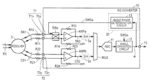
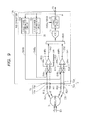
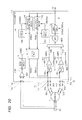
- FIG. 1 is a block diagram showing the configuration of an R/D converter 10 as a semiconductor device according to a first embodiment
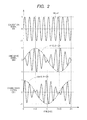
- FIG. 2 is a view showing examples of an excitation signal EX input to a resolver 3 , as well as a sine wave signal SN 1 and a cosine wave signal CS 1 that are output from the resolver 3 ;
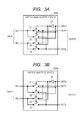
- FIGS. 3A and 3B are circuit diagrams showing an example of the configuration and operation of a switching circuit SWa of FIG. 1 ;
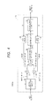
- FIG. 4 is a block diagram showing an example of the configuration of an angle operation circuit 12 of FIG. 1 ;
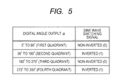
- FIG. 5 is a view of the relationship between the input and output values in a table format with respect to an angle range determination circuit 13 of FIG. 1 ;
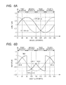
- FIGS. 6A and 6B are graphs showing the relationship between the amplitude and the angle ⁇ with respect to a sine wave signal SN 1 and a cosine wave signal CS 1 ;
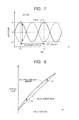
- FIG. 7 is a waveform diagram of the sine wave signal SN 1 and the cosine wave signal CS 1 when the electrical angle ⁇ is 135 degrees;
- FIG. 8 is a view for illustrating the non-linearity error of an A/D converter
- FIG. 9 is a block diagram showing the configuration of an R/D converter 10 A according to a second embodiment
- FIG. 10 is a view of the relationship between the input and output values in a table format with respect to respective angle range determination circuits 13 A and 13 B of FIG. 9 ;
- FIG. 11 is a graph of the relationship between the amplitude and the angle ⁇ with respect to a sine wave signal SN 2 and a cosine wave signal CS 2 that are input to an A/D converter 11 , in the R/D converter 10 A of FIG. 9 ;
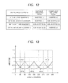
- FIG. 12 shows the relationship between the input and output values in a table format, in a variation of the angle range determination circuits 13 A and 13 B of FIG. 9 ;
- FIG. 13 is a graph of the relationship between the amplitude and the angle ⁇ with respect to the sine wave signal SN 2 and the cosine wave signal CS 2 that are input to the A/D converter 11 , in a variation of the second embodiment;
- FIG. 14 is a block diagram showing the configuration of an R/D converter 10 B according to a third embodiment
- FIG. 15 is a timing diagram showing the operation waveforms of the respective parts shown in FIG. 14 ;
- FIG. 16 shows waveforms of the sine wave signal SN 2 which was output from an amplifier AMPa shown in FIG. 14 ;
- FIG. 17 is a block diagram showing the configuration of an R/D converter 10 C according to a fourth embodiment
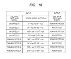
- FIG. 18 is a view of the relationship between the input and output values in a table format with respect to the angle range determination circuit 13 of FIG. 17 ;
- FIG. 19 shows waveforms of the sine wave signal SN 2 which was output from the amplifier AMPa shown in FIG. 17 ;
- FIG. 20 is a block diagram showing the configuration of an R/D converter 10 D according to a fifth embodiment
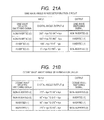
- FIGS. 21A and 21B are views showing the relationship between the input and output values in a table format with respect to the respective angle range determination circuits 13 A and 13 B of FIG. 20 ;
- FIG. 22 is a block diagram showing the configuration of a motor control device.
- FIG. 1 is a block diagram showing the configuration of an R/D converter 10 as a semiconductor device according to a first embodiment. Note that in the first embodiment, the R/D converter is described as an example of the semiconductor device. However, as described in a sixth embodiment, it is also possible to configure the semiconductor device by an integrated circuit (for example, a micro controller unit) including R/D converter.
- an integrated circuit for example, a micro controller unit
- the R/D converter 10 includes input parts T 1 and T 2 , an output part T 3 , amplifiers AMPa and AMPb, resistance elements R 13 , R 14 , R 23 , and R 24 , a switching circuit SWa, a multiplexer MUX, an A/D converter 11 , an angle operation circuit 12 , and an angle range determination circuit 13 .
- the R/D converter 10 calculates the angle ⁇ based on the sine wave signal SN 1 and on the cosine wave signal CS 1 that are received from the resolver 3 .
- the configuration of the respective parts of the resolver 3 and the R/D converter 10 will be described below.
- the resolver 3 includes one rotor winding and two stator windings.
- the two stator windings are mechanically displaced, for example, by an angle of 90 degrees from each other.
- an excitation signal EX is input to the rotor winding
- the sine wave signal SN 1 obtained by modulating the excitation signal EX by the sine of the electrical angle
- the cosine wave signal CS 1 obtained by modulating the excitation signal EX by the cosine of the electrical angle
- FIG. 2 is a view showing an example of the excitation signal EX input to the resolver 3 of FIG. 1 , as well as the sine wave signal SN 1 and the cosine wave signal CS 1 that are output from the resolver 3 .
- the axial double angle is set to 1.
- positive-side input terminal T 1 p and negative-side input terminal T 1 n of the input part T 1 are coupled to the resolver 3 , respectively, through resistance elements R 11 and R 12 .
- the input part T 1 receives the differential sine wave signal SN 1 .
- Positive-side input terminal T 2 p and negative-side input terminal T 2 n of the input part T 2 are coupled to the resolver 3 , respectively, through resistance elements R 21 and R 22 .
- the input part T 2 receives the differential cosine wave signal CS 1 .
- the amplifiers AMPa and AMPb are, for example, operation amplifiers.
- the non-inverting input terminal (positive terminal) of the amplifier AMPa is coupled to the positive side input terminal T 1 p of the input part T 1 through the switching circuit SWa.
- the inverting input terminal (negative terminal) of the amplifier AMPa is coupled to the negative side input terminal T 1 n of the input part T 1 through the switching circuit SWa.
- the inverting input terminal (negative terminal) of the amplifier AMPa is also coupled to the output terminal of the amplifier AMPa through the resistance element R 13 .
- the non-inverting input terminal (positive terminal) of the amplifier AMPa is coupled to a node that gives a common potential com through the resistance element R 14 .
- the non-inverting input terminal (positive terminal) of the amplifier AMPb is coupled to the positive side input terminal T 2 p of the input part T 2
- the inverting input terminal (negative terminal) of the amplifier AMPb is coupled to the negative side input terminal T 2 n of the input part T 2
- the inverting input terminal (negative terminal) of the amplifier AMPb is also coupled to the output terminal of the amplifier AMPb through the resistance element R 23 .
- the non-inverting input terminal (positive terminal) of the amplifier AMPb is also coupled to a node that gives the common potential com through the resistance element R 24 .
- the amplifier AMPa when the resistance elements R 11 and R 12 are equal in size and when the resistance elements R 13 and R 14 are equal in size, the amplifier AMPa outputs the signal obtained by subtracting the potential of the negative side input terminal T 1 n of the input part T 1 from the potential of the positive side input terminal T 1 p of the input part T 1 . In other words, it outputs the single-end sine wave signal SN 2 obtained by amplifying the differential sine wave signal SN 1 .
- the amplifier AMPb outputs the signal obtained by subtracting the potential of the negative side input terminal T 2 n of the input terminal T 2 from the potential of the positive side input terminal T 2 p of the input part T 2 . In other words, it outputs the single-end cosine wave signal CS 2 obtained by amplifying the differential cosine wave signal CS 1 .
- the switching circuit SWa is provided between the input part T 1 and the amplifier AMPa.
- the switching circuit SWa When the switching signal SWSa is in the active state, the switching circuit SWa reverses the plus and minus sides of the sine wave signal SN 1 which is a differential signal, namely, inverts the value of the sine wave signal SN 1 , and inputs to the amplifier AMPa.
- the switching circuit SWa when the switching signal SWSa is in the inactive state, the switching circuit SWa does not invert the sine wave signal SN 1 and inputs the sine wave signal SN 1 to the amplifier AMPa.
- the former case is referred to as that the switching circuit SWa is in the inverted state
- the latter case is referred to as that the switching circuit SWa is in the non-inverted state.
- the logic level of the switching signal SWSa is high level (H level) or “1” when the switching signal SWSa is in the active state. Further, it is assumed that the logic level of the switching signal SWSa is low level (L level) or “0” when the switching signal SWSa is in the inactive state.
- H level high level
- L level low level
- FIGS. 3A and 3B are circuit diagrams showing an example of the configuration and operation of the switching circuit SWa shown in FIG. 1 .
- the switching circuit SWa includes switching elements 21 to 24 and an inverter 25 .
- the switching element 21 is coupled between an input node INn and an output node OUTn.
- the switching element 22 is coupled between the input node INn and an output node OUTp.
- the switching element 23 is coupled between an input node INp and the output node OUTn.
- the switching element 24 is coupled between the input node INp and the output node OUTp.
- Each of the switching elements 21 to 24 is configured, for example, with a P-type meta oxide semiconductor (MOS) transistor.
- the switch element is conductive when the control electrode receives an active control signal.
- the switching element is non-conductive when the control electrode receives an inactive control signal.
- a signal obtained by inverting the logic level of the switching signal SWSa by the inverter 25 is input as the control signal to the switching elements 21 and 24 .
- the switching signal SWSa is input as the control signal to the switching elements 22 and 23 .
- the multiplexer MUX alternately selects the sine wave signal SN 2 output from the amplifier AMPa and the cosine wave signal CS 2 output from the amplifier AMPb. Then, the multiplexer MUX outputs the selected signal to the A/D converter 11 .
- the switching time when the multiplexer MUX alternately switches the signals is set to the time required for converting the analog value sampled by the A/D converter 11 into the value of one angle ⁇ , which is, for example, about one hundredth the cycle (2 ⁇ / ⁇ ) of the excitation signal EX.
- sample & hold (S/H) circuits 9 a , 9 b may be provided between the multiplexer MUX and the respective amplifiers AMPa and AMPb.
- the A/D converter (ADC: Analog to Digital Converter) 11 converts the sine wave signal SN 2 and the cosine wave signal CS 2 , which are selected by the multiplexer MUX, into digital values.
- ADC Analog to Digital Converter
- a sequential transformation method, or the like, can be used as the A/D converter 11 .
- FIG. 4 is a block diagram showing an example of the configuration of the angle operation circuit 12 shown in FIG. 1 .
- the angle operation circuit 12 has a known configuration, including a sin/cos distribution circuit 32 , multiplication circuits 33 and 34 , a subtraction circuit 35 , a synchronous detection circuit 36 , a compensator 37 , an accumulation counter 38 , a cosine read only memory (ROM) 39 , and a sine ROM 40 .
- EX is sin ( ⁇ t) and the electrical angle of the rotor is ⁇ .
- the sin/cos distribution circuit 32 distributes the output of the A/D converter 11 into the sine wave signal SN 2 (sin ⁇ sin ⁇ t) and the cosine wave signal CS 2 (cos ⁇ sin ⁇ t). At this time, when the sine wave signal SN 2 is inverted based on the switching signal SWSa, it is multiplied by minus one and returned to the original value.
- the multiplication circuit 33 multiplies the sine wave signal SN 2 (sin ⁇ sin ⁇ t) and the cosine (cos ⁇ ) of the calculated angle ⁇ .
- the multiplication circuit 34 multiplies the cosine wave signal CS 2 (cos ⁇ sin ⁇ t) and the sine (sin ⁇ ) of the calculated angle ⁇ .
- the cosine ROM 39 outputs the cosine (cos ⁇ ) of the current angle ⁇ , based on the relationship between the various angles ⁇ stored in advance and the cosine (cos ⁇ ) of the respective angles.
- the sine ROM 40 outputs the sine (sin ⁇ ) of the current angle ⁇ , based on the relationship between the various angles ⁇ stored in advance and the sine (sin ⁇ ) of the respective angles.
- the subtraction circuit 35 calculates the deviation ⁇ 1 by subtracting the output of the multiplication circuit 34 from the output of the multiplication circuit 33 .
- the deviation ⁇ 1 is given by the following equation:
- the output of the synchronous detection circuit 36 is counted by the accumulation counter 38 through the compensator 37 .
- the angle ⁇ is calculated.
- the angle range determination circuit 13 is a logic circuit for generating the switching signal SWSa based on the calculated angle ⁇ .
- the switching circuit SWa is switched so that the sine wave signal SN 2 and the cosine wave signal CS 2 , which are input to the A/D converter 11 , have the same phase.
- the angle range determination circuit 13 configures a switch control circuit 20 that controls the switching timing of the switching circuit SWa. Further details will be described below with reference to FIGS. 1 and 5 .
- FIG. 5 is a view showing the relationship between the input and output values in a table format with respect to the angle range determination circuit 13 of FIG. 1 .
- the angle range determination circuit 13 is configured with a circuit that refers to the second highest bit value and outputs the bit value as the switching signal SWSa.
- the R/D converter 10 of FIG. 1 calculates the angle ⁇ based on the input sine wave signal SN 1 and on the input cosine wave signal CS 1 .
- the angle range determination circuit 13 is provided in the R/D converter 10 to switch the switching signal SWSa between active and inactive according to the range of the calculated angle ⁇ .
- the switching circuit SWa changes to the inverted state, so that the sine wave signal SN 1 is inverted (in such a way that the signal on the positive side and the signal on the negative side are reversed). More specifically, when the angle ⁇ is in the second quadrant (90 to 180 degrees) or the fourth quadrant (270 to 360 degrees), the switching circuit SWa is controlled to be brought into the inverted state.
- the angle ⁇ is in the second quadrant (90 to 180 degrees) or the fourth quadrant (270 to 360 degrees)
- the switching circuit SWa is controlled to be brought into the inverted state.
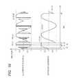
- FIGS. 6A and 6B are graphs showing the relationship between the amplitude and the angle ⁇ with respect to the sine wave signal and the cosine wave signal.
- FIG. 6A shows the relationship between the amplitude and the angle ⁇ of the sine wave signal SN 1 (sin ⁇ ) and the cosine wave signal CS 1 (cos ⁇ ) that are input to the R/D converter 10 .
- FIG. 6B shows the relationship between the amplitude and the angle ⁇ of the sine wave signal SN 2 (sin ⁇ or ⁇ sin ⁇ ) and the cosine wave signal CS 2 (cos ⁇ ) that are input to the A/D converter 11 .
- the sine wave signal SN 2 input to the A/D converter 11 is switched to the signal ( ⁇ sin ⁇ ) obtained by inverting the original sine wave signal SN 1 (sin ⁇ ) by the switching circuit SWa.
- the values of the sine wave signal SN 2 and the cosine wave signal CS 2 which are input to the A/D converter 11 , can be closer to each other than the previous values before input to the R/D converter 10 .
- FIG. 7 shows the waveforms of the sine wave signal SN 1 and the cosine wave signal CS 1 when the electrical angle ⁇ is 135 degrees.
- the sine wave signal SN 1 (A ⁇ sin ⁇ t) and the cosine wave signal CS 1 ( ⁇ A ⁇ sin ⁇ t), which are input to the R/D converter 10 are the same in amplitude but reversed in phase to each other.
- the sine wave signal SN 1 is inverted in the switching circuit SWa, so that the sine wave signal SN 2 ( ⁇ A ⁇ sin ⁇ t) and the cosine wave signal CS 2 ( ⁇ A ⁇ sin ⁇ t), which are input to the A/D converter 11 , are exactly the same.
- the calculated angle ⁇ is exactly equal to 135 degrees.
- the sine wave signal SN 1 (A ⁇ sin ⁇ t) and the cosine wave signal CS 1 ( ⁇ A ⁇ sin ⁇ t), which are input to the R/D converter 10 , remain unchanged and are input to the A/D converter 11 .
- the sine wave signal output from the A/D converter 11 is A ⁇ sin ⁇ t+ ⁇ 1
- the cosine wave signal output from the A/D converter 11 is ⁇ A ⁇ sin ⁇ t+ ⁇ 2. Because ⁇ 1 is not equal to ⁇ 2, the angle ⁇ output from the angle operation circuit 12 is not 135 degrees and an angle error occurs.
- the sine wave signal when the electrical angle ⁇ is 135 and 315 degrees, the sine wave signal is inverted.
- the sine wave signal and the cosine wave signal are the same in value when they are obtained by the A/D converter 10 .
- the sine wave signal is returned to the original value by multiplying the sine wave signal by minus one by the angle calculation circuit 12 , the sine wave signal is correctly equal to the cosine wave signal multiplied with minus one. This eliminates the angle conversion error due to the non-linearity error of the A/D converter 11 .
- the switching circuit SWa is provided to invert the sine wave signal.
- the sine wave signal and the cosine wave signal, which are input to the A/D converter 11 are typically the same in phase and their values are close to each other, so that they are not likely to be affected by the nonlinearity error of the A/D converter 11 .
- the switching circuit SWb between the input part T 2 and the amplifier AMPb, instead of between the input part T 1 and the amplifier AMPa, to allow the cosine wave signal CS 1 , instead of the sine wave signal SN 1 , to be inverted.
- the switching circuit SWb inverts the cosine wave signal CS 1 when the range of the angle ⁇ is the second quadrant (90 to 180 degrees) and the fourth quadrant (270 to 360 degrees).
- FIG. 9 is a block diagram showing the configuration of an R/D converter 10 A according to a second embodiment.
- the R/D converter 10 A of the second embodiment is different from the R/D converter 10 of FIG. 1 in that the switching circuit SWb is further provided between the input part T 2 and the amplifier AMPb.
- the angle range determination circuit 13 A for controlling the switching circuit SWa based on the calculated angle ⁇
- the angle range determination circuit 13 B for controlling the switching circuit SWb based on the angle ⁇ . Since the example of the configuration of the switching circuits SWa, SWb is the same as that described in FIGS. 3A and 3B , the description thereof will not be repeated. Note that the angle range determination circuits 13 A and 13 B configure the switch control circuit 20 that controls the switching timing of the switching circuits SWa and SWb.
- FIG. 10 is a view of the relationship between the input and output values in a table format with respect to the angle range determination circuits 13 A and 13 B of FIG. 9 .
- the sine wave signal SN 2 or the cosine wave signal CS 2 is inverted according to the angle ⁇ so that both the sine wave signal SN 2 and the cosine wave signal CS 2 , which are input to the A/D converter 11 , are greater than the common potential com.
- the angle range determination circuit 13 A for the sine wave activates (“1”) the switching signal SWSa to bring the switching circuit SWa for the sine wave signal SN 1 into the inverted state.
- the angle range determination circuit 13 A inactivates (“0”) the switching signal SWSa to bring the switching circuit SWa for the sine wave signal SN 1 into the non-inverted state.
- the angle range determination circuit 13 B for the cosine wave activates (“1”) the switching signal SWSb to bring the switching circuit SWb for the cosine wave signal CS 2 into the inverted state.
- the angle range determination circuit 13 B inactivates (“0”) the switching signal SWSb to bring the switching circuit SWb for the cosine wave signal CS 1 into the non-inverted state.
- the angle range determination circuit 13 A is configured with a circuit that refers to the highest bit and outputs the value as the switching signal SWSa.
- the angle range determination circuit 13 B is configured with a logic circuit that refers to the highest bit value and the next highest bit value, calculates the XOR sum of the two values, and outputs the result as the switching signal SWSb.
- the angle operation circuit 12 multiplies the sine wave signal SN 1 and the cosine wave signal CS 1 by minus one to return to their original values before inversion.
- FIG. 9 The other configurations in FIG. 9 are the same as those in FIG. 1 , so that like or corresponding parts are indicated by like reference numerals as used in FIG. 1 and the description thereof will not be repeated.
- FIG. 11 is a graph of the relationship between the amplitude and the angle ⁇ of the sine wave signal SN 2 and the cosine wave signal CS 2 that are input to the A/D convert 11 in the R/D converter 10 A of FIG. 9 .
- the potential of the sine wave signal SN 2 greatly varies at 90 and 270 degrees, which are the angles ⁇ at which the switching circuit SWa is switched. Because of this noise occurs, which is a factor of the angle error.
- the amplitude of the sine wave signal SN 1 or cosine wave signal CS 1 to be inverted is 0 at 90, 180, and 270 degrees, which are the angles ⁇ at which the switching circuit SWa or SWb is switched. This reduces the occurrence of noise, and thus it is possible to reduce the angle error compared to the case of the first embodiment.
- FIG. 12 is a view of the relationship between the input and output values in a table format, in the variation of the respective angle range determination circuits 13 A and 13 B shown in FIG. 9 .
- the sine wave signal SN 2 or the cosine wave signal CS 2 is inverted according to the angle ⁇ , so that both the sine wave signal SN 2 and the cosine wave signal CS 2 , which are input to the A/D converter 11 , are smaller than the common potential com.
- the angle range determination circuit 13 A for the sine wave activates (“1”) the switching signal SWSa to bring the switching circuit SWa for the sine wave signal SN 1 into the inverted state.
- the angle range determination circuit 13 A inactivates (“0”) the switching signal SWSa to bring the switching circuit SWa for the sine wave signal SN 1 into the non-inverted state.
- the angle range determination circuit 13 B for the cosine wave activates (“1”) the switching signal SWSb to bring the switching circuit SWb for the cosine wave signal CS 1 into the inverted state.
- the angle range determination circuit 13 B inactivates (“0”) the switching signal SWSb to bring the switching circuit SWb for the cosine wave signal CS 2 into the non-inverted state.
- the angle range determination circuit 13 A is configured with a logic circuit for referring to the highest bit, generating an inverted signal of the bit value, and outputting the inverted signal as the switching signal SWSa.
- the angle range determination circuit 13 B is configured with a logic circuit for referring to the highest bit value and the next highest bit value, generating an inverted signal of the XOR sum of the two values, and outputting the inverted signal as the switching signal SWSb.
- FIG. 13 is a graph of the relationship between the amplitude and the angle ⁇ of the sine wave signal SN 2 and the cosine wave signal CS 2 that are input to the A/D converter 11 , in the variation of the second embodiment.
- the amplitude of the sine wave signal SN 1 or cosine wave signal CS 1 to be inverted is 0 at 90, 180, and 270 degrees, which are the angles ⁇ at which the switching circuit SWa or SWb is switched. This reduces the occurrence of noise, and thus it is possible to reduce the angle error compared to the case of the first embodiment.
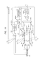
- FIG. 14 is a block diagram showing the configuration of an R/D converter 10 B according to a third embodiment.
- the R/D converter 10 B of FIG. 14 is different from the R/D converter of FIG. 1 in that a comparator CMP, an edge detection circuit 14 , and a latch circuit 15 are further included.
- the comparator CMP compares the positive side signal and negative side signal of the differential excitation signal EX. When the value of the excitation signal EX is positive, the comparator CMP outputs the comparison signal CMS of high level (H level). While when the excitation signal EX is negative, the comparator CMP outputs the comparison signal CMS of low level (L level).
- the edge detection circuit 14 detects the rising edge and falling edge of the comparison signal CMS output from the comparator CMP.
- the edge detection circuit 14 outputs a one-shot pulse (excitation edge signal EXEG) at the timing of the rising edge and falling edge of the comparison signal CMS.
- EXEG excitation edge signal
- the latch circuit 15 holds a switching signal SWSa 1 output from the angle range determination circuit 13 , and outputs the switching signal SWSa 1 in synchronization with the timing of the excitation edge signal EXEG output from the edge detection circuit 14 .
- the switching circuit SWa switches between the inverted state and the non-inverted state in response to the switching signal SWSa 2 output from the latch circuit 15 .
- the timing of switching between the inverted state and the non-inverted state in the switching circuit SWa is synchronized with the timing of the zero crossing point of the excitation signal EX.
- the angle range determination circuit 13 the comparator CMP, the edge detection circuit 14 , and the latch circuit 15 configure the switch control circuit 20 that controls the timing of the switching of the switching circuit SWa.
- FIG. 15 is a timing diagram showing the operation waveforms of the respective parts shown in FIG. 14 .
- the comparison signal CMS, the excitation edge signal EXEG, and the switching signals SWSa 1 and SWSa 2 in FIG. 14 are shown beginning at the top.
- the edge of the comparison signal CMS is detected at times t 1 , t 3 , and t 6 in FIG. 15 . Then, the one-shot pulse is output as the excitation edge signal EXEG.
- the switching signal SWSa 1 is switched from L level to H level at time t 2 .
- the timing of the rise of the switching signal SWSa 2 output from the latch circuit 15 is delayed until time t 4 when the excitation edge signal EXEG is activated (switched to H level).
- the switching signal SWSa 1 is switched from H level to L level at time t 5 .
- the timing of the fall of the switching signal SWSa 2 output from the latch circuit 15 is delayed until time t 7 when the excitation edge signal EXEG is activated (switched to H level).
- FIG. 16 shows waveforms of the sine wave signal SN 2 which was output from the amplifier AMPa, wherein waveform (A) represents a comparative example and waveform (B) represents the present embodiment.
- waveform (A) represents a comparative example
- waveform (B) represents the present embodiment.
- the excitation signal EX is sin ⁇ t and the electrical angle ⁇ is approximately 90 degrees.
- the sine wave signal SN 1 input to the R/D converter 10 B is approximately equal to sin ⁇ t
- the cosine wave signal CS 1 is approximately 0.
- the electrical angle ⁇ is slightly smaller than 90 degrees before time t 12
- the electrical angle ⁇ is slightly greater than 90 degrees after time t 12 .
- Waveform (A) is a comparative example of the sine wave signal SN 2 input to the A/D converter 11 in this case.
- the electrical angle ⁇ passes through 90 degrees to move from the first quadrant to the second quadrant.
- the sine wave signal SN 2 is changed to the signal obtained by inverting the input sine wave signal SN 1 after time t 12 .
- the sine wave signal SN 2 significantly changes and noise occurs, which may result in an error in the finally calculated angle ⁇ .
- waveform (B) of the present embodiment the timing of the switching of the switching circuit SWa is delayed until time t 13 which is the zero crossing point of the excitation signal EX. For this reason, at the timing of switching at time t 13 , the sine wave signal SN 2 is approximately 0 and significant signal change does not occur. As a result, it is possible to reduce the noise associated with the switching of the switching circuit SWa, and to reduce the angle conversion error.
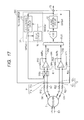
- FIG. 17 is a block diagram showing the configuration of an R/D converter 10 C according to a fourth embodiment.
- the R/D converter 10 C of FIG. 17 is different from the R/D converter 10 of the first embodiment in FIG. 1 in that a delay circuit 16 is further included.
- the delay circuit 16 includes a flip-flop, and the like.
- the delay circuit 16 generates and outputs a delayed switching signal DSWSa 1 .
- the delayed switching signal DSWSa 1 is a signal obtained by delaying the switching signal SWSa output from the angle range determination circuit 13 by at least one cycle of clock.
- the R/D converter 10 C of FIG. 17 is different from the R/D converter 10 of FIG. 1 with respect to the operation of the angle range determination circuit 13 .
- the angle range determination circuit 13 of FIG. 17 generates the switching signal SWSa 1 based on the angle ⁇ that is calculated by the angle operation circuit 12 , and on the delayed switching signal DSWSa 1 .
- the output of the angle range determination circuit 13 has a hysteresis effect that depends not only on the current angle ⁇ but also on the logic level of the previous switching signal SWSa 1 .
- the angle range determination circuit 13 and the delay circuit 16 configure the switch control circuit 20 that controls the timing of the switching of the switching circuit SWa.
- FIG. 18 is a view of the relationship between the input and output values in a table format with respect to the angle range determination circuit 13 of FIG. 17 .
- hys is the predetermined angle (for example, about several times the angle resolution) that indicates the width of the hysteresis.
- the switching signal SWSa 1 at least before one cycle (namely, the delayed switching signal DSWSa 1 ) is in the active state (“1”).
- the switching circuit SWa does not change to the non-inverted state.
- the switching circuit SWa switches to the non-inverted state.
- the switching signal SWSa 1 before at least one cycle (namely, the delayed switching signal DSWSa 1 ) is in the inactive state (“0”).
- the switching circuit SWa does not change to the inverted state.
- the switching circuit SWa switches to the inverted state.
- the angle range determination circuit 13 detects that the sine wave signal SN 1 and the cosine wave signal CS 1 , which are input to the respective input parts T 1 and T 2 , change from the same phase to the reverse phase or from the reverse phase to the same phase, based on the calculated angle ⁇ . In this case, the angle range determination circuit 13 switches between activation/inactivation of the switching signal SWSa at the timing when the calculated angle ⁇ further changes by the predetermined angle hys, from the time when the same phase and the reverse phase are switched.
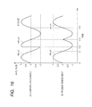
- FIG. 19 shows waveforms of the sine wave signal SN 2 which was output from the amplifier AMPa of FIG. 17 , wherein waveform (A) represents a comparative example and waveform (B) represents the present embodiment.
- waveform (A) represents a comparative example
- waveform (B) represents the present embodiment.
- the excitation signal EX is sin ⁇ t and the electrical angle ⁇ is approximately 90 degrees.
- the sin wave signal SN 1 input to the R/D converter 10 B is approximately equal to sin ⁇ t and the cosine wave signal CS 1 is approximately 0.
- the electrical angle ⁇ is slightly smaller than 90 degrees from time t 0 to time t 1 . Then, the electrical angle ⁇ is slightly greater than 90 degrees after time t 1 . Thus, the sine wave signal SN 2 is inverted to ⁇ sin ⁇ t at time t 1 . Further, the electrical angle ⁇ is slightly greater than 90 degrees until the next time t 2 . Then, the electrical angle ⁇ is slightly smaller than 90 degrees after time t 2 . Thus, the sine wave signal SN 2 is inverted to sin ⁇ t at time t 2 .
- the sine wave signal SN 2 is inverted to ⁇ sin ⁇ t at time t 3 , sin ⁇ t at time t 4 , ⁇ sin ⁇ t at time t 5 , sin ⁇ t at time t 6 , and ⁇ sin ⁇ t at time t 7 .
- the switching circuit SWa switches frequently and the sine wave signal SN 2 significantly changes every time the switching circuit SWa switches. The noise may occur due to the significant signal change, resulting in the angle conversion error.
- the sine wave signal SN 2 is switched only when the detected angle ⁇ further changes by the predetermined angle hys. More specifically, at the time when the electrical angle ⁇ reaches 90 degrees plus hys at time t 7 , the sine wave signal SN 2 is inverted to ⁇ sin ⁇ t. Further, at the time when the electrical angle ⁇ reaches to 90 degrees minus hys at time t 8 , the sine wave signal SN 2 is inverted to sin ⁇ t. In this way, even if the electrical angle ⁇ fluctuates around the 90 degrees, it is possible to reduce the number of times the switching circuit SWa switches. As a result, it is possible to reduce the occurrence of noise and to reduce the angle conversion error.
- a fifth embodiment is a combination of the second to fourth embodiments.
- FIG. 20 is a block diagram showing the configuration of an R/D converter 10 D according to the fifth embodiment.
- the R/D converter 10 D of FIG. 20 is different from the R/D converter 10 A of the second embodiment described in FIG. 9 , in that delay circuits 16 A and 16 B, the comparator CMP, the edge detection circuit 14 , and the latch circuit 15 are further included.
- the delay circuit 16 A generates and outputs the delayed switching signal DSWSa 1 as described in FIG. 17 .
- the delayed switching signal DSWSa 1 is a signal obtained by delaying the switching signal SWSa 1 , which is output from the angle range determination circuit 13 A, by at least one cycle of clock.
- the delay circuit 16 B generates and outputs a delayed switching signal DSWSb 1 .
- the delayed switching signal DSWSb 1 is a signal obtained by delaying the switching signal SWSb 1 , which is output from the angle range determination circuit 13 B, by at least one cycle of clock.
- the angle range determination circuit 13 A has a hysteresis effect.
- the angle range determination circuit 13 A generates the switching signal SWSa 1 based on the angle ⁇ calculated by the angle operation circuit 12 and on the delayed switching signal DSWSa 1 .
- the angle range determination circuit 13 B generates the switching signal SWSb 1 based on the angle ⁇ calculated by the angle operation circuit 12 and on the delayed switching signal DSWSb 1 .
- the comparator CMP and the edge detection circuit 14 are the same as those described in FIG. 14 , so that the description thereof will not be repeated.
- the latch circuit 15 holds the switching signal SWSa 1 output from the angle range determination circuit 13 A. Then, the latch circuit 15 outputs the switching signal SWSa 1 in synchronization with the timing of the activation of the excitation edge signal EXEG output from the edge detection circuit 14 (namely, in synchronization with the zero crossing point of the excitation signal EX).
- the switching circuit SWa switches between the inverted state and the non-inverted state in response to the switching signal SWSa 2 output from the latch circuit 15 .
- the latch circuit 15 holds the switching signal SWSb 1 output from the angle range determination circuit 13 B.
- the latch circuit 15 outputs the switching signal SWSa 1 in synchronization with the timing of the activation of the excitation edge signal EXEG output from the edge detection circuit 14 (namely, in synchronization with the zero crossing point of the excitation signal EX).
- the switching circuit SWb switches between the inverted state and the non-inverted state in response to the switching signal SWSb 2 output from the latch circuit 15 .
- the angle operation circuit 12 multiplies the sine wave signal SN 1 and the cosine wave signal CN 1 by minus one to return to their original values before inversion. Since the other configurations in FIG. 20 are the same as those in FIG. 1 , like or corresponding parts are indicated by like reference numerals as used in FIG. 1 and the description thereof will not be repeated.
- the angle range determination circuits 13 A and 13 B, the comparator CMP, the edge detection circuit 14 , the latch circuit 15 , and the delay circuits 16 A and 16 B configure the switch control circuit 20 that controls the timing of the switching of the switching circuits SWa and SWb.
- FIGS. 21A and 21B are views showing the relationship between the input and output values in a table format with respect to the angle range determination circuits 13 A and 13 B.
- the switching signal SWSa 1 for the sine wave before at least one cycle (namely, the delayed switching signal DSWSa 1 ) is in the active state (“1”), even if the angle ⁇ corresponds to the boundary of the entire first and second quadrants (0 to 180 degrees), the switching signal SWSa 1 does not change to the inactive state.
- the switching signal SWSa 1 changes to the inactive state at the time when the angle ⁇ further changes by the angle hys from the boundary of the entire first and second quadrants.
- the switching circuit SWa changes from the inverted state to the non-inverted state at the timing of the zero crossing point of the excitation signal EX.
- the switching signal SWSa 1 for the sine wave before at least one cycle (namely, the delayed switching signal DSWSa 1 ) is in the inactive state (“0”)
- the switching signal SWSa 1 does not change to the active state.
- the switching signal SWSa 1 changes to the active state at the time when the angle ⁇ further changes by the angle hys from the boundary of the entire third and fourth quadrants.
- the switching circuit SWa changes from the non-inverted state to the inverted state at the timing of the zero crossing point of the excitation signal EX.
- the switching signal SWSb 1 for the cosine wave before at least one cycle (namely, the delayed switching signal DSWSb 1 ) is in the active state (“1”), even if the angle ⁇ corresponds to the boundary of the entire fourth and first quadrants (270 to 90 degrees), the switching signal SWSb 1 does not change to the inactive state.
- the switching signal SWSb 1 changes to the inactive state at the time when the angle ⁇ further changes by the angle hys from the entire fourth and first quadrants.
- the switching circuit SWb changes from the inverted state to the non-inverted state at the timing of the zero crossing point of the excitation signal EX.
- the switching signal SWSb 1 for the cosine wave before at least one cycle (namely, the delayed switching signal DSWSb 1 ) is in the inactive state (“0”)
- the switching signal SWSb 1 does not change to the active state.
- the switching signal SWSb 1 changes to the active state at the time when the angle ⁇ further changes by the angle hys from the boundary of the entire second and third quadrants.
- the switching circuit SWb changes from the non-inverted state to the inverted state at the timing of the zero crossing point of the excitation signal EX.
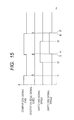
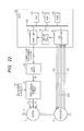
- FIG. 22 is a block diagram showing the configuration of a motor control device.
- the resolver 3 is often used as a sensor for detecting the angle of a rotational axis 2 of the synchronous motor 1 .
- the motor control device controls the rotary drive of the synchronous motor 1 based on the detected value of the resolver 3 .
- the motor control device includes a micro controller unit (MCU) 100 , a pre-driver 110 , and a three-phase inverter circuit 111 .
- MCU micro controller unit
- the micro controller unit 100 includes a central processing unit (CPU) 101 , a random access memory (RAM) 102 , a read only memory (ROM) 103 , a PWM timer 104 , a motor control circuit 106 , the R/D converter 10 described in the first to fifth embodiments, and a bus 105 for coupling each of the components.
- the excitation signal EX is output to the resolver 3 from the R/D converter 10 .
- the sine wave signal SN 1 and the cosine wave signal CS 1 are input to the R/D converter 10 from the resolver 3 .
- the CPU 101 controls the entire MCU 100 by executing a control program stored in advance in the ROM 103 .
- the RAM 102 is used as a work memory of the CPU 101 .
- An electrically rewritable memory, such as a flash memory, can be used as the ROM 103 .
- the motor control circuit 106 receives the angle ⁇ output from the R/D converter 10 , and performs various processes for the feedback control of the motor based on the angle ⁇ .
- the PWM timer 104 receives the control signal from the motor control circuit 106 , and outputs a three-phase pulse width modulation (PWM) signal for controlling the U/V/W phases of the synchronous motor 1 .
- Control registers are provided in each of the R/D converter 10 , the motor control circuit 106 , and the PWM timer to control them by themselves. Then, the CPU 101 sets values to the respective control registers through the bus 105 .
- the pre-driver 110 generates and outputs a gate control signal for controlling the open and close of six switching elements (for example, insulated gate bipolar transistors (IGBT)), not shown, that configure the three-phase inverter circuit 111 .
- IGBT insulated gate bipolar transistors
- the three-phase inverter circuit 111 converts the DC voltage from a DC power supply 112 into a three-phase voltage (motor drive voltage) based on the gate control signal output from the pre-driver 110 .
- the three-phase inverter circuit 111 drives the motor by supplying the DC voltage of each phase to each phase winding.
Landscapes
- Engineering & Computer Science (AREA)
- Theoretical Computer Science (AREA)
- Physics & Mathematics (AREA)
- General Physics & Mathematics (AREA)
- Transmission And Conversion Of Sensor Element Output (AREA)
- Control Of Motors That Do Not Use Commutators (AREA)
Priority Applications (1)
| Application Number | Priority Date | Filing Date | Title |
|---|---|---|---|
| US16/031,872 US10530383B2 (en) | 2015-01-29 | 2018-07-10 | Semiconductor device |
Applications Claiming Priority (2)
| Application Number | Priority Date | Filing Date | Title |
|---|---|---|---|
| JP2015-015618 | 2015-01-29 | ||
| JP2015015618A JP6527704B2 (ja) | 2015-01-29 | 2015-01-29 | 半導体装置 |
Related Child Applications (1)
| Application Number | Title | Priority Date | Filing Date |
|---|---|---|---|
| US16/031,872 Division US10530383B2 (en) | 2015-01-29 | 2018-07-10 | Semiconductor device |
Publications (2)
| Publication Number | Publication Date |
|---|---|
| US20160226508A1 US20160226508A1 (en) | 2016-08-04 |
| US10033397B2 true US10033397B2 (en) | 2018-07-24 |
Family
ID=55272334
Family Applications (2)
| Application Number | Title | Priority Date | Filing Date |
|---|---|---|---|
| US14/991,978 Active 2036-04-14 US10033397B2 (en) | 2015-01-29 | 2016-01-10 | Semiconductor device |
| US16/031,872 Active US10530383B2 (en) | 2015-01-29 | 2018-07-10 | Semiconductor device |
Family Applications After (1)
| Application Number | Title | Priority Date | Filing Date |
|---|---|---|---|
| US16/031,872 Active US10530383B2 (en) | 2015-01-29 | 2018-07-10 | Semiconductor device |
Country Status (4)
| Country | Link |
|---|---|
| US (2) | US10033397B2 (ja) |
| EP (1) | EP3054598A1 (ja) |
| JP (1) | JP6527704B2 (ja) |
| CN (1) | CN105841603B (ja) |
Families Citing this family (11)
| Publication number | Priority date | Publication date | Assignee | Title |
|---|---|---|---|---|
| WO2016018383A1 (en) | 2014-07-31 | 2016-02-04 | Hewlett-Packard Development Company | Live migration of data |
| US10540109B2 (en) | 2014-09-02 | 2020-01-21 | Hewlett Packard Enterprise Development Lp | Serializing access to fault tolerant memory |
| WO2016064417A1 (en) | 2014-10-24 | 2016-04-28 | Hewlett Packard Enterprise Development Lp | End-to-end negative acknowledgment |
| WO2016122642A1 (en) | 2015-01-30 | 2016-08-04 | Hewlett Packard Enterprise Development Lp | Determine failed components in fault-tolerant memory |
| US10409681B2 (en) | 2015-01-30 | 2019-09-10 | Hewlett Packard Enterprise Development Lp | Non-idempotent primitives in fault-tolerant memory |
| WO2016122610A1 (en) | 2015-01-30 | 2016-08-04 | Hewlett Packard Enterprise Development Lp | Preventing data corruption and single point of failure in a fault-tolerant memory |
| US10402261B2 (en) | 2015-03-31 | 2019-09-03 | Hewlett Packard Enterprise Development Lp | Preventing data corruption and single point of failure in fault-tolerant memory fabrics |
| US10193634B2 (en) | 2016-09-19 | 2019-01-29 | Hewlett Packard Enterprise Development Lp | Optical driver circuits |
| US10389342B2 (en) * | 2017-06-28 | 2019-08-20 | Hewlett Packard Enterprise Development Lp | Comparator |
| JP7251751B2 (ja) * | 2017-11-07 | 2023-04-04 | 株式会社松尾製作所 | 電気角取得システム、電気角取得方法、電気角取得プログラム、電気角取得特性測定システム、電気角取得特性測定方法および電気角取得特性測定プログラム |
| US11722343B1 (en) * | 2022-05-13 | 2023-08-08 | Hamilton Sundstrand Corporation | Resolver integral demodulation using zero crossing points |
Citations (16)
| Publication number | Priority date | Publication date | Assignee | Title |
|---|---|---|---|---|
| US3516084A (en) * | 1967-07-17 | 1970-06-02 | Sperry Rand Corp | Analog-to-digital converter |
| US3594783A (en) * | 1969-08-07 | 1971-07-20 | Giddings & Lewis | Apparatus for numerical signaling of positions, including digital-to-analog converter |
| US3713141A (en) * | 1971-05-21 | 1973-01-23 | Us Navy | Synchro-to-digital conversion method and apparatus |
| US3843877A (en) * | 1973-02-06 | 1974-10-22 | Sperry Rand Corp | Air data computer including dc to synchro signal converter |
| US4149260A (en) | 1977-09-14 | 1979-04-10 | General Motors Corporation | Analog to digital converter for providing the digital representation of an angle |
| US4281316A (en) * | 1978-08-11 | 1981-07-28 | The Singer Company | Successive approximation S/D converter with inherent quantization error centering |
| US4334179A (en) * | 1980-06-16 | 1982-06-08 | Sperry Corporation | Apparatus for demodulating a pulse excited synchro position sensor |
| US4556885A (en) * | 1982-01-26 | 1985-12-03 | Tokyo Shibaura Denki Kabushiki Kaisha | System for detecting position or speed |
| US4594540A (en) * | 1984-10-03 | 1986-06-10 | The United States Of America As Represented By The Administrator Of The National Aeronautics And Space Administration | Angular measurement system |
| EP0333070A2 (fr) | 1988-03-16 | 1989-09-20 | Tecnospace S.A. | Procédé de numérisation de la valeur d'un angle défini par ses coordonnées trigonométriques sinus et cosinus |
| US6525502B1 (en) * | 1999-09-02 | 2003-02-25 | Aspen Motion Technologies, Inc. | Closed loop control of motor position and velocity |
| JP2004309285A (ja) | 2003-04-07 | 2004-11-04 | Minebea Co Ltd | R/dコンバータ |
| US20050030010A1 (en) * | 2001-10-30 | 2005-02-10 | Jones Ross Peter | Sensing apparatus and method |
| US7352305B2 (en) * | 2005-08-11 | 2008-04-01 | Mitutoyo Corporation | Method and circuit for interpolating encoder output |
| US20100097052A1 (en) * | 2008-10-16 | 2010-04-22 | Lillestolen Kirk A | Resolver interface and signal conditioner |
| US20150330812A1 (en) * | 2012-12-10 | 2015-11-19 | Continental Automotive France | Position-detecting unit having reduced offset voltage, and method using such a unit |
Family Cites Families (13)
| Publication number | Priority date | Publication date | Assignee | Title |
|---|---|---|---|---|
| JPS49117755U (ja) * | 1973-02-09 | 1974-10-08 | ||
| JPS6243501A (ja) * | 1985-08-20 | 1987-02-25 | Kobe Steel Ltd | 角度検出装置 |
| JPH0375522A (ja) * | 1989-08-18 | 1991-03-29 | Anritsu Corp | レゾルバ/ディジタルコンバータ |
| JP2004279231A (ja) * | 2003-03-17 | 2004-10-07 | Minebea Co Ltd | R/dコンバータ |
| KR100634588B1 (ko) * | 2003-12-30 | 2006-10-13 | 현대자동차주식회사 | 영구자석 동기모터 제어시스템 및 제어방법 |
| US8639996B2 (en) * | 2008-07-11 | 2014-01-28 | Qualcomm Incorporated | Systems and methods for uplink inter-cell interference cancellation using hybrid automatic repeat request (HARQ) retransmissions |
| JP2011257254A (ja) * | 2010-06-09 | 2011-12-22 | Hitachi Automotive Systems Ltd | 回転角検出装置 |
| JP5281126B2 (ja) * | 2011-07-15 | 2013-09-04 | 三菱電機株式会社 | レゾルバによる角度検出方法 |
| JP2013160720A (ja) * | 2012-02-08 | 2013-08-19 | Denso Corp | 回転角検出装置 |
| JP5802588B2 (ja) * | 2012-03-23 | 2015-10-28 | 株式会社東芝 | 角度検出装置およびモータ駆動制御装置 |
| US9068861B2 (en) * | 2012-08-24 | 2015-06-30 | Hamilton Sundstrand Corporation | Resolver interface |
| CN202841081U (zh) * | 2012-10-26 | 2013-03-27 | 浙江工贸职业技术学院 | 基于cordic算法的dds波形发生器 |
| CN103178809B (zh) * | 2013-02-04 | 2016-02-17 | 深圳市鼎阳科技有限公司 | 一种dds脉冲边沿调节方法、模块和脉冲信号发生器 |
-
2015
- 2015-01-29 JP JP2015015618A patent/JP6527704B2/ja active Active
-
2016
- 2016-01-10 US US14/991,978 patent/US10033397B2/en active Active
- 2016-01-20 CN CN201610036818.8A patent/CN105841603B/zh active Active
- 2016-01-29 EP EP16153378.1A patent/EP3054598A1/en not_active Ceased
-
2018
- 2018-07-10 US US16/031,872 patent/US10530383B2/en active Active
Patent Citations (16)
| Publication number | Priority date | Publication date | Assignee | Title |
|---|---|---|---|---|
| US3516084A (en) * | 1967-07-17 | 1970-06-02 | Sperry Rand Corp | Analog-to-digital converter |
| US3594783A (en) * | 1969-08-07 | 1971-07-20 | Giddings & Lewis | Apparatus for numerical signaling of positions, including digital-to-analog converter |
| US3713141A (en) * | 1971-05-21 | 1973-01-23 | Us Navy | Synchro-to-digital conversion method and apparatus |
| US3843877A (en) * | 1973-02-06 | 1974-10-22 | Sperry Rand Corp | Air data computer including dc to synchro signal converter |
| US4149260A (en) | 1977-09-14 | 1979-04-10 | General Motors Corporation | Analog to digital converter for providing the digital representation of an angle |
| US4281316A (en) * | 1978-08-11 | 1981-07-28 | The Singer Company | Successive approximation S/D converter with inherent quantization error centering |
| US4334179A (en) * | 1980-06-16 | 1982-06-08 | Sperry Corporation | Apparatus for demodulating a pulse excited synchro position sensor |
| US4556885A (en) * | 1982-01-26 | 1985-12-03 | Tokyo Shibaura Denki Kabushiki Kaisha | System for detecting position or speed |
| US4594540A (en) * | 1984-10-03 | 1986-06-10 | The United States Of America As Represented By The Administrator Of The National Aeronautics And Space Administration | Angular measurement system |
| EP0333070A2 (fr) | 1988-03-16 | 1989-09-20 | Tecnospace S.A. | Procédé de numérisation de la valeur d'un angle défini par ses coordonnées trigonométriques sinus et cosinus |
| US6525502B1 (en) * | 1999-09-02 | 2003-02-25 | Aspen Motion Technologies, Inc. | Closed loop control of motor position and velocity |
| US20050030010A1 (en) * | 2001-10-30 | 2005-02-10 | Jones Ross Peter | Sensing apparatus and method |
| JP2004309285A (ja) | 2003-04-07 | 2004-11-04 | Minebea Co Ltd | R/dコンバータ |
| US7352305B2 (en) * | 2005-08-11 | 2008-04-01 | Mitutoyo Corporation | Method and circuit for interpolating encoder output |
| US20100097052A1 (en) * | 2008-10-16 | 2010-04-22 | Lillestolen Kirk A | Resolver interface and signal conditioner |
| US20150330812A1 (en) * | 2012-12-10 | 2015-11-19 | Continental Automotive France | Position-detecting unit having reduced offset voltage, and method using such a unit |
Non-Patent Citations (1)
| Title |
|---|
| Extended European Search Report dated Jul. 7, 2016, in European Patent Application No. EP16153378.1. |
Also Published As
| Publication number | Publication date |
|---|---|
| US20160226508A1 (en) | 2016-08-04 |
| US20180323797A1 (en) | 2018-11-08 |
| EP3054598A1 (en) | 2016-08-10 |
| CN105841603B (zh) | 2020-11-10 |
| CN105841603A (zh) | 2016-08-10 |
| US10530383B2 (en) | 2020-01-07 |
| JP2016138870A (ja) | 2016-08-04 |
| JP6527704B2 (ja) | 2019-06-05 |
Similar Documents
| Publication | Publication Date | Title |
|---|---|---|
| US10530383B2 (en) | Semiconductor device | |
| US9255817B2 (en) | Rotation-angle detection device, image processing apparatus, and rotation-angle detection method | |
| JP5919730B2 (ja) | モータ駆動制御装置及び方法 | |
| US8427089B2 (en) | Motor driving device | |
| JP2007104768A (ja) | モータ制御装置及びモータ制御方法 | |
| US20030062868A1 (en) | Switching methodology for ground referenced voltage controlled electric machine | |
| JP2017093065A5 (ja) | ||
| JP2008116350A (ja) | 回転角検出装置及び回転角検出方法 | |
| Chen et al. | M/T method based incremental encoder velocity measurement error analysis and self-adaptive error elimination algorithm | |
| JPS62171100A (ja) | レゾルバ制御方法 | |
| KR101422427B1 (ko) | 전력 변환 장치 | |
| US9035592B2 (en) | Apparatus and method for controlling speed of motor | |
| US9473054B2 (en) | Angle detection apparatus, motor driving control apparatus and angle detection method | |
| US10158306B2 (en) | Three-phase brushless motor state identification | |
| JP6361428B2 (ja) | 電圧レベル検出装置及び方法、モータ駆動制御装置、及びモータ装置 | |
| CN109217745B (zh) | 计算装置和处理装置 | |
| CN116569456A (zh) | 马达驱动装置 | |
| JP6405512B2 (ja) | レゾルバ励磁信号の異常検出装置及び方法 | |
| US11368108B2 (en) | Method and apparatus for determining the intermediate circuit current of a converter | |
| TW201902121A (zh) | 脈波寬度調變轉換器及其轉換方法 | |
| WO2024004474A1 (ja) | 角度検出装置および角度検出方法 | |
| JP2017207382A (ja) | 電子制御装置 | |
| JP2015114159A (ja) | 回転信号処理回路 | |
| JP3131975B2 (ja) | ディジタル三相pwm波形発生装置 | |
| Wang et al. | FPGA-based interpolation for motor encoders |
Legal Events
| Date | Code | Title | Description |
|---|---|---|---|
| AS | Assignment |
Owner name: RENESAS ELECTRONICS CORPORATION, JAPAN Free format text: ASSIGNMENT OF ASSIGNORS INTEREST;ASSIGNORS:KUROOKA, KAZUAKI;FUNATO, YOSHIHIRO;REEL/FRAME:037540/0058 Effective date: 20150828 |
|
| STCF | Information on status: patent grant |
Free format text: PATENTED CASE |
|
| MAFP | Maintenance fee payment |
Free format text: PAYMENT OF MAINTENANCE FEE, 4TH YEAR, LARGE ENTITY (ORIGINAL EVENT CODE: M1551); ENTITY STATUS OF PATENT OWNER: LARGE ENTITY Year of fee payment: 4 |