US10027228B2 - Switching converter having noise cancellation feature and electronic device using the same - Google Patents
Switching converter having noise cancellation feature and electronic device using the same Download PDFInfo
- Publication number
- US10027228B2 US10027228B2 US15/311,316 US201515311316A US10027228B2 US 10027228 B2 US10027228 B2 US 10027228B2 US 201515311316 A US201515311316 A US 201515311316A US 10027228 B2 US10027228 B2 US 10027228B2
- Authority
- US
- United States
- Prior art keywords
- transistor
- switching
- transistors
- smoothing circuit
- switching converter
- Prior art date
- Legal status (The legal status is an assumption and is not a legal conclusion. Google has not performed a legal analysis and makes no representation as to the accuracy of the status listed.)
- Active
Links
Images


Classifications
-
- H—ELECTRICITY
- H02—GENERATION; CONVERSION OR DISTRIBUTION OF ELECTRIC POWER
- H02M—APPARATUS FOR CONVERSION BETWEEN AC AND AC, BETWEEN AC AND DC, OR BETWEEN DC AND DC, AND FOR USE WITH MAINS OR SIMILAR POWER SUPPLY SYSTEMS; CONVERSION OF DC OR AC INPUT POWER INTO SURGE OUTPUT POWER; CONTROL OR REGULATION THEREOF
- H02M3/00—Conversion of DC power input into DC power output
- H02M3/02—Conversion of DC power input into DC power output without intermediate conversion into AC
- H02M3/04—Conversion of DC power input into DC power output without intermediate conversion into AC by static converters
- H02M3/10—Conversion of DC power input into DC power output without intermediate conversion into AC by static converters using discharge tubes with control electrode or semiconductor devices with control electrode
- H02M3/145—Conversion of DC power input into DC power output without intermediate conversion into AC by static converters using discharge tubes with control electrode or semiconductor devices with control electrode using devices of a triode or transistor type requiring continuous application of a control signal
- H02M3/155—Conversion of DC power input into DC power output without intermediate conversion into AC by static converters using discharge tubes with control electrode or semiconductor devices with control electrode using devices of a triode or transistor type requiring continuous application of a control signal using semiconductor devices only
- H02M3/156—Conversion of DC power input into DC power output without intermediate conversion into AC by static converters using discharge tubes with control electrode or semiconductor devices with control electrode using devices of a triode or transistor type requiring continuous application of a control signal using semiconductor devices only with automatic control of output voltage or current, e.g. switching regulators
- H02M3/158—Conversion of DC power input into DC power output without intermediate conversion into AC by static converters using discharge tubes with control electrode or semiconductor devices with control electrode using devices of a triode or transistor type requiring continuous application of a control signal using semiconductor devices only with automatic control of output voltage or current, e.g. switching regulators including plural semiconductor devices as final control devices for a single load
-
- H—ELECTRICITY
- H02—GENERATION; CONVERSION OR DISTRIBUTION OF ELECTRIC POWER
- H02M—APPARATUS FOR CONVERSION BETWEEN AC AND AC, BETWEEN AC AND DC, OR BETWEEN DC AND DC, AND FOR USE WITH MAINS OR SIMILAR POWER SUPPLY SYSTEMS; CONVERSION OF DC OR AC INPUT POWER INTO SURGE OUTPUT POWER; CONTROL OR REGULATION THEREOF
- H02M1/00—Details of apparatus for conversion
- H02M1/44—Circuits or arrangements for compensating for electromagnetic interference in converters or inverters
-
- H—ELECTRICITY
- H02—GENERATION; CONVERSION OR DISTRIBUTION OF ELECTRIC POWER
- H02M—APPARATUS FOR CONVERSION BETWEEN AC AND AC, BETWEEN AC AND DC, OR BETWEEN DC AND DC, AND FOR USE WITH MAINS OR SIMILAR POWER SUPPLY SYSTEMS; CONVERSION OF DC OR AC INPUT POWER INTO SURGE OUTPUT POWER; CONTROL OR REGULATION THEREOF
- H02M3/00—Conversion of DC power input into DC power output
- H02M3/02—Conversion of DC power input into DC power output without intermediate conversion into AC
- H02M3/04—Conversion of DC power input into DC power output without intermediate conversion into AC by static converters
- H02M3/10—Conversion of DC power input into DC power output without intermediate conversion into AC by static converters using discharge tubes with control electrode or semiconductor devices with control electrode
- H02M3/145—Conversion of DC power input into DC power output without intermediate conversion into AC by static converters using discharge tubes with control electrode or semiconductor devices with control electrode using devices of a triode or transistor type requiring continuous application of a control signal
- H02M3/155—Conversion of DC power input into DC power output without intermediate conversion into AC by static converters using discharge tubes with control electrode or semiconductor devices with control electrode using devices of a triode or transistor type requiring continuous application of a control signal using semiconductor devices only
-
- H—ELECTRICITY
- H05—ELECTRIC TECHNIQUES NOT OTHERWISE PROVIDED FOR
- H05K—PRINTED CIRCUITS; CASINGS OR CONSTRUCTIONAL DETAILS OF ELECTRIC APPARATUS; MANUFACTURE OF ASSEMBLAGES OF ELECTRICAL COMPONENTS
- H05K1/00—Printed circuits
- H05K1/02—Details
- H05K1/0213—Electrical arrangements not otherwise provided for
- H05K1/0216—Reduction of cross-talk, noise or electromagnetic interference
- H05K1/0228—Compensation of cross-talk by a mutually correlated lay-out of printed circuit traces, e.g. for compensation of cross-talk in mounted connectors
-
- H—ELECTRICITY
- H02—GENERATION; CONVERSION OR DISTRIBUTION OF ELECTRIC POWER
- H02M—APPARATUS FOR CONVERSION BETWEEN AC AND AC, BETWEEN AC AND DC, OR BETWEEN DC AND DC, AND FOR USE WITH MAINS OR SIMILAR POWER SUPPLY SYSTEMS; CONVERSION OF DC OR AC INPUT POWER INTO SURGE OUTPUT POWER; CONTROL OR REGULATION THEREOF
- H02M3/00—Conversion of DC power input into DC power output
- H02M3/003—Constructional details, e.g. physical layout, assembly, wiring or busbar connections
-
- H—ELECTRICITY
- H02—GENERATION; CONVERSION OR DISTRIBUTION OF ELECTRIC POWER
- H02M—APPARATUS FOR CONVERSION BETWEEN AC AND AC, BETWEEN AC AND DC, OR BETWEEN DC AND DC, AND FOR USE WITH MAINS OR SIMILAR POWER SUPPLY SYSTEMS; CONVERSION OF DC OR AC INPUT POWER INTO SURGE OUTPUT POWER; CONTROL OR REGULATION THEREOF
- H02M7/00—Conversion of AC power input into DC power output; Conversion of DC power input into AC power output
- H02M7/003—Constructional details, e.g. physical layout, assembly, wiring or busbar connections
-
- H—ELECTRICITY
- H05—ELECTRIC TECHNIQUES NOT OTHERWISE PROVIDED FOR
- H05K—PRINTED CIRCUITS; CASINGS OR CONSTRUCTIONAL DETAILS OF ELECTRIC APPARATUS; MANUFACTURE OF ASSEMBLAGES OF ELECTRICAL COMPONENTS
- H05K1/00—Printed circuits
- H05K1/02—Details
- H05K1/0213—Electrical arrangements not otherwise provided for
- H05K1/0216—Reduction of cross-talk, noise or electromagnetic interference
- H05K1/023—Reduction of cross-talk, noise or electromagnetic interference using auxiliary mounted passive components or auxiliary substances
- H05K1/0231—Capacitors or dielectric substances
Definitions
- the present invention relates to a switching converter having switching elements.
- DC/DC converters switching regulators
- AC/DC converters AC/DC converters
- DC/DC converters switching regulators
- AC/DC converters AC/DC converters
- DC/DC converters are designed to step down a direct current (DC) voltage supplied from a battery or inverter to an optimal voltage level for load.
- AC/DC converters are designed to convert an alternating current (AC) voltage into a corresponding DC voltage.
- FIG. 1 is a circuit diagram illustrating a configuration example of a switching converter 2 r studied by the present inventors.
- the switching converter 2 r illustrated in FIG. 1 is a step-down DC/DC converter and primarily includes an output circuit 10 and a control circuit (controller) 20 .
- the switching converter 2 steps down an input voltage V IN of an input line 4 to a given level, supplying an output voltage V OUT to a load (not shown) connected to an output line 8 .
- the output circuit 10 includes an input capacitor C 1 , an output capacitor C 2 , a high-side transistor (switching transistor) M 1 , a low-side transistor (synchronous rectification transistor) M 2 , and an inductor L 1 .
- the input capacitor C 1 is provided between the input line 4 and a ground line 6 to stabilize the input voltage V IN .
- the output capacitor C 2 is connected between the output line 8 and the ground line 6 to smooth the output voltage V OUT .
- the high-side transistor M 1 and the low-side transistor M 2 are connected in series between the input line 4 and the ground line 6 , i.e., in parallel with the input capacitor C 1 .
- the inductor L 1 is provided between a switching node (or also referred to as a switching line) 9 and the output line 8 .
- the switching node is a connection point between the high-side transistor M 1 and the low-side transistor M 2 .
- the controller 20 is supplied with a feedback voltage V FB that is proportional to the output voltage V OUT .
- the controller 20 generates a pulse signal whose duty ratio is adjusted so that the feedback voltage V FB approaches a given reference voltage V REF .
- the controller 20 generates a gate voltage HG for the high-side transistor M 1 and a gate voltage LG for the low-side transistor M 2 in accordance with the pulse signal, complementarily switching between the high-side transistor M 1 and the low-side transistor M 2 with a dead time provided between the switching events. Switching between the high-side transistor M 1 and the low-side transistor M 2 is controlled by the controller 20 , stabilizing the output voltage V OUT to a target level.
- the present inventor has recognized the following problem as a result of study of the switching converter 2 r illustrated in FIG. 1 .
- FIG. 2 is an operation waveform diagram of the switching converter 2 r illustrated in FIG. 1 .
- FIG. 2 shows the input voltage V IN and a voltage (referred to as a switching voltage) V SW of the switching node 9 .
- V IN input voltage
- V SW switching voltage
- the gate voltages HG and LG are at low and high levels, respectively, with the high-side transistor M 1 and the low-side transistor M 2 being OFF and ON, respectively.
- the gate voltage HG of the high-side transistor M 1 goes up to high level, and the gate voltage LG of the low-side transistor M 2 goes down to low level.
- the high-side transistor M 1 turns fully ON and remains ON, and the low-side transistor M 2 turns OFF, causing the switching voltage V SW to be substantially equal to the input voltage V IN .
- switching between the high-side transistor M 1 and the low-side transistor M 2 is controlled in such a manner that a dead time is provided between the switching events. However, such a dead time is ignored here.
- the switching converter 2 r illustrated in FIG. 1 has a current loop that includes the input capacitor C 1 , the output capacitor C 2 , the high-side transistor M 1 , and the low-side transistor M 2 .
- a current including high-frequency components resulting from switching between the high-side transistor M 1 and the low-side transistor M 2 flows into the current loop including the input capacitor C 1 , the high-side transistor M 1 , and the low-side transistor M 2 , thus resulting in ringing of the input voltage V IN and the switching voltage V SW .
- the ringing frequency is often about several tens to hundreds of MHz, for example.
- the present invention has been devised in light of the foregoing, and it is an illustrative object of a mode of the present invention to provide a switching converter that contributes to reduce EMI.
- a mode of the present invention relates to a switching converter.
- the switching converter includes a smoothing circuit and first and second transistors.
- the smoothing circuit includes at least one capacitor.
- the first and second transistors are connected in series between two ends of the smoothing circuit.
- the first and second transistors are arranged side by side in a first direction on a circuit board.
- Two current loops that run through the smoothing circuit and the first and second transistors are formed to be substantially linearly symmetrical with respect to an axis of symmetry that extends in the first direction.
- Another mode of the present invention relates to an electronic device.
- the electronic device includes one of the above switching converters.
- the present invention contributes to reduce EMI of switching converters.
- FIG. 1 is a circuit diagram illustrating a configuration example of a switching converter studied by the present inventor et al.
- FIG. 2 is an operation waveform diagram of the switching converter illustrated in FIG. 1 .
- FIG. 3 is a circuit diagram of a switching converter according to a first embodiment.
- FIG. 4 is a basic layout diagram of the switching converter illustrated in FIG. 3 .
- FIG. 5 is a diagram illustrating the operating principle of the switching converter according to the first embodiment.
- FIG. 6( a ) is a diagram illustrating a pin assignment of a power module
- FIG. 6( b ) is a diagram illustrating an internal layout thereof.
- FIG. 7 is a specific layout diagram of the switching converter illustrated in FIG. 3 .
- FIG. 8 is a layout diagram of a switching converter according to a comparative technology.
- FIGS. 9( a ) and 9( b ) are diagrams illustrating measurement results of magnetic fields near the switching converters illustrated respectively in FIGS. 7 and 8 .
- FIGS. 10( a ) and 10( b ) are diagrams illustrating calculation results of magnetic fields near the switching converters illustrated respectively in FIGS. 8 and 7 .
- FIG. 11 is a diagram illustrating the relationship between the distance in the Z direction and the magnetic field strength
- ⁇ square root over ( ) ⁇ (Bx 2 +By 2 +Bz 2 ).
- FIG. 12 is a circuit diagram of a switching converter according to a second embodiment.
- FIG. 13 is a layout diagram of the switching converter illustrated in FIG. 12 .
- FIGS. 14( a ) and 14( b ) are, respectively, a circuit diagram and a layout diagram of a switching converter according to a first modification example.
- FIGS. 15( a ) and 15( b ) are layout diagrams of switching converters according to a second modification example.
- FIG. 16 is a layout diagram of a switching converter according to a third modification example.
- FIGS. 17( a ) to 17( c ) are circuit diagrams of modification examples of switching converters.
- FIG. 18 is a block diagram illustrating a configuration of an electronic device incorporating a switching converter.
- the expression “the condition in which a member A is connected to a member B” includes not only physical and direct connection of the member A to the member B but also indirect connection of the members A and B via other member that does not affect the electrical connection condition.
- the expression “the condition in which a member C is provided between the members A and B” includes not only direct connection of the members A and C or the members B and C but also indirect connection of the members A and C or the members B and C via other member that does not affect the electrical connection condition.
- FIG. 3 is a circuit diagram of a switching converter 2 according to a first embodiment.
- the switching converter 2 is similar in basic configuration to its counterpart shown in FIG. 1 .
- an even number of input capacitors such as two input capacitors C 1 a and C 1 b are connected in parallel between the input line 4 and the ground line 6 .
- the input capacitors C 1 a and C 1 b are referred to as an input smoothing circuit 12 .
- the high-side transistor (first transistor) M 1 and the low-side transistor (second transistor) M 2 may be packaged in a single power module 14 as illustrated in FIG. 3 .
- the power module 14 includes a drain terminal P 1 , a source terminal P 2 , a switching terminal P 3 , and a first gate terminal P 4 , and a second gate terminal P 5 .
- the drain terminal P 1 is connected to one end (drain) of the high-side transistor M 1 .
- the source terminal P 2 is connected to one end (source) of the low-side transistor M 2 .
- the switching terminal P 3 is connected to a switching terminal, a connection node between the high-side transistor M 1 and the low-side transistor M 2 .
- the drain terminal P 1 is connected to the input line 4 .
- the source terminal P 2 is connected to the ground line 6 .
- the switching terminal P 3 is connected to the inductor L 1 via a switching line 9 .
- Gate drive voltages HG and LG from the controller 20 are fed to the first and second gate terminals P 4 and P 5 , respectively.
- the high-side transistor M 1 may be a P-channel MOSFET.
- an insulated gate bipolar transistor (IGBT) or a bipolar transistor may be used rather than a MOSFET.
- FIG. 4 is a basic layout diagram of the switching converter 2 illustrated in FIG. 3 . It should be noted that only part of the output circuit 10 of the switching converter 2 is shown here for simple description and easy understanding.
- the high-side transistor M 1 and the low-side transistor M 2 are arranged side by side in a first direction (X direction) on a circuit board 30 . Then, a current loop 50 that runs through the smoothing circuit 12 , the high-side transistor M 1 , and the low-side transistor M 2 branches into two current loops 50 a and 50 b . These loops are formed to be substantially linearly symmetrical with respect to an axis of symmetry 32 that extends in the first direction (X direction).
- the input line 4 and the ground line 6 are formed as printed circuits on the circuit board 30 .
- the input smoothing circuit 12 includes the two capacitors C 1 a and C 1 b .
- the two capacitors C 1 a and C 1 b are arranged symmetrically with the mounting area of the high-side transistor M 1 and the low-side transistor M 2 , in other words, the mounting area of the power module 14 , provided therebetween.
- the wiring pattern (layout) of the input line 4 and the ground line 6 is designed so that the first and second current loops 50 a and 50 b are linearly symmetrical with respect to the axis of symmetry 32 .
- the first current loop 50 a runs through the one capacitor C 1 a , the high-side transistor M 1 , and the low-side transistor M 2 .
- the second current loop 50 b runs through the other capacitor C 1 b , the high-side transistor M 1 , and the low-side transistor M 2 .
- FIG. 5 is a diagram illustrating the operating principle of the switching converter 2 according to the first embodiment. Because of the symmetrical layout, currents flow in opposite directions in the first and second current loops 50 a and 50 b . As a result, magnetic flux densities Ba and Bb induced by the currents flowing through each of the current loops 50 a and 50 b are opposite in direction.
- the magnetic flux densities Ba and Bb cancel out at an arbitrary point near the power module 14 , thus contributing to reduce electromagnetic noise or EMI as compared to formation of a single current loop.
- FIG. 6( a ) is a diagram illustrating a pin assignment of the power module 14
- FIG. 6( b ) is a diagram illustrating an internal layout thereof.
- the high-side transistor M 1 and the low-side transistor M 2 are arranged side by side in the first direction (X direction) inside the power module 14 .
- the high-side transistor M 1 and the low-side transistor M 2 may be integrated in a single die (chip) or may be individually integrated in two separate dies.
- the drain terminal P 1 , the source terminal P 2 , and the switching terminal P 3 are arranged in the first direction (X direction).
- the drain terminal P 1 , the source terminal P 2 , and the switching terminal P 3 should preferably be arranged adjacent to each other in the first direction.
- the drain terminal P 1 and the source terminal P 2 may be interchanged.
- asymmetrical dual N-channel MOSFET FDPC8016S
- Fairchild asymmetrical dual N-channel MOSFET
- FIG. 7 is a specific layout diagram of the switching converter 2 illustrated in FIG. 3 .
- the power module 14 having the pin assignment shown in FIG. 6( a ) is used.
- Each of the input line 4 and the ground line 6 has a portion that extends in a second direction (Y direction) perpendicular to the first direction (X direction) near the mounting areas of the input smoothing circuit 12 and the power module 14 . More specifically, the input line 4 and the ground line 6 are formed to overlap the drain terminal P 1 and the source terminal P 2 , respectively.
- the switching line 9 may be formed in parallel with the input line 4 and the ground line 6 in such a manner as to overlap the switching terminal P 3 .
- the input capacitors C 1 a and C 1 b are arranged side by side in the Y direction in such a manner as to sandwich the power module 14 .
- One end of each of the input capacitors C 1 a and C 1 b is connected to the input line 4 , with the other end thereof connected to the ground line 6 .
- the two current loops 50 a and 50 b are formed that are substantially linearly symmetrical about the axis of symmetry 32 . As described with reference to FIG. 5 , therefore, the magnetic fluxes generated by the two current loops 50 a and 50 b cancel each other out, thus contributing to reduce EMI.
- FIG. 8 is a layout diagram of the switching converter 2 r according to a comparative technology.
- the input smoothing circuit 12 includes two input capacitors C 1 b and C 1 c that are arranged adjacent to each other. In this case, two current loops 50 b and 50 c are formed to substantially overlap each other and interlink with a common magnetic flux.
- the current loop 50 b runs through the input capacitor C 1 b and the transistors M 1 and M 2 .
- the current loop 50 c runs through the input capacitor C 1 c and the transistors M 1 and M 2 .
- the magnetic fluxes generated by the current loops 50 b and 50 c strengthen each other, thus resulting in higher EMI.
- FIGS. 9( a ) and 9( b ) are diagrams illustrating measurement results of magnetic fields near the switching converters 2 and 2 r illustrated respectively in FIGS. 7 and 8 .
- the magnetic fields were measured 10 mm away from the surface of the power module 14 using a near magnetic field tester (EMI tester: Peritec's EMV-200).
- EMI tester Peritec's EMV-200
- an improvement of about 1.3 dB is observed in the layout shown in FIG. 7 over the layout shown in FIG. 8 .
- FIGS. 10( a ) and 10( b ) are diagrams illustrating calculation results of magnetic fields near the switching converters 2 r and 2 illustrated respectively in FIGS. 8 and 7 .
- the measured points were positioned 10 mm away from the surface of the power module 14 .
- an improvement of up to 7.4 dB is observed by arranging the two current loops symmetrically if the magnetic flux Bz in the Z direction is considered.
- FIG. 11 is a diagram illustrating the relationship between the distance in the Z direction and the magnetic field strength
- ⁇ square root over ( ) ⁇ (Bx 2 +By 2 +Bz 2 ).
- (i) is a curve for the layout shown in FIG. 7
- a closed loop formed by a smoothing circuit and two transistors branches into two loops.
- the smoothing circuit includes capacitors.
- the two transistors are connected in series between the two ends of the smoothing circuit.
- the two loops are laid out in a linearly symmetrical manner. This layout contributes to reduce EMI.
- the following advantage can be obtained by using the power module 14 whose drain terminal P 1 and source terminal P 2 are arranged adjacent to each other as illustrated in FIG. 6( a ) as compared to the layout illustrated in FIG. 4 .
- the drain terminal P 1 and the source terminal P 2 are not adjacent to each other, with the switching terminal P 3 arranged at the center.
- the switching line 9 to be connected to the switching terminal P 3 must straddle the input line 4 or the ground line 6 . In order to do so, it is necessary to form part of wiring on the rear face of the circuit board 30 and connect the switching line 9 to the switching terminal P 3 by means of via holes.
- via holes are not preferred because they lead to a difficult-to-predict parasitic inductance.
- drain terminal P 1 and the source terminal P 2 adjacent to each other contributes to a smaller current loop area, in other words, smaller impedance within the current loop, thus reducing power noise accompanied by high-frequency ringing and cutting down the absolute value of EMI.
- FIG. 12 is a circuit diagram of a switching converter 2 a according to a second embodiment.
- the switching converter 2 a is similar in basic configuration to its counterpart shown in FIG. 3 .
- a plurality of N, and specifically an even number of, and more specifically two, power modules 14 a and 14 b are connected in parallel between the input line 4 and the ground line 6 .
- the high-side transistor M 1 includes two transistors M 1 a and M 1 b that are connected in parallel
- the low-side transistor M 2 includes two transistors M 2 a and M 2 b that are connected in parallel.
- FIG. 13 is a layout diagram of the switching converter 2 a illustrated in FIG. 12 .
- the input smoothing circuit 12 including the input capacitor C 1 is arranged on the axis of symmetry 32 , and the two power modules 14 a and 14 b are arranged to be linearly symmetrical with respect to the axis of symmetry 32 in such a manner as to sandwich the input smoothing circuit 12 .
- the two transistors (not shown) inside the power module 14 a are arranged side by side in the X direction.
- the two transistors (not shown) inside the power module 14 b are arranged side by side in the X direction.
- the input smoothing circuit 12 may include the plurality of input capacitors C 1 as in FIG. 3 . In this case, it is only necessary to arrange the plurality of input capacitors C 1 adjacent to each other in the first direction (Y direction).
- the two current loops 50 a and 50 b are also formed that are substantially linearly symmetrical about the axis of symmetry 32 . As described with reference to FIG. 5 , therefore, the magnetic fluxes generated by the two current loops 50 a and 50 b cancel each other out, thus contributing to reduce EMI.
- the high-side transistor (first transistor) M 1 and the low-side transistor (second transistor) M 2 are packaged in a single power module.
- the present invention is not limited thereto. That is, the high-side transistor M 1 and the low-side transistor M 2 may be discrete elements that are packaged separately.
- FIGS. 14( a ) and 14( b ) are, respectively, a circuit diagram and a layout diagram of a switching converter 2 e according to a first modification example.
- the equivalent circuit is similar to that shown in FIG. 12 except that the transistors M 1 a and M 2 a of the power module 14 a and the transistors M 1 b and M 2 b of the power module 14 b are separate elements.
- FIGS. 15( a ) and 15( b ) are layout diagrams of switching converters 2 f and 2 g according to a second modification example.
- the switching converter 2 f illustrated in FIG. 15( a ) uses the two power modules 14 a and 14 b whose pin assignments are bilaterally symmetrical in the switching converter 2 a illustrated in FIG. 13 .
- the input smoothing circuit 12 includes the input capacitor C 1 . It should be noted that the input smoothing circuit 12 may include a plurality of input capacitors arranged side by side in the first direction in the present modification example.
- the switching converter 2 g illustrated in FIG. 15( b ) uses the discrete elements M 1 a and M 1 b , and M 2 a and M 2 b whose pin assignments are bilaterally symmetrical in the switching converter 2 e illustrated in FIG. 14( b ) .
- having bilaterally symmetrical pin assignments contributes to an even smaller current loop area, in other words, smaller impedance within the current loops, thus reducing power noise accompanied by high-frequency ringing and cutting down the absolute value of EMI.
- FIG. 16 is a layout diagram of a switching converter 2 h according to a third modification example.
- the first transistor M 1 and the second transistor M 2 are arranged side by side on a first face of the circuit board.
- the input capacitor C 1 of the smoothing circuit 12 is arranged on the axis of symmetry 32 on a second face, the rear side of the first face of the circuit board. Wiring on the first and second faces is electrically connected by means of via holes (through holes) VH.
- FIGS. 17( a ) to 17( c ) are circuit diagrams of modification examples of the switching converter 2 .
- a switching converter 2 b illustrated in FIG. 17( a ) is a step-up DC/DC converter.
- the switching transistor (first transistor) M 1 and the synchronous rectification transistor (second transistor) M 2 are provided in series between the two ends of an output smoothing circuit 16 that includes the output capacitor C 2 . Therefore, it is only necessary to lay out the current loop formed by the output smoothing circuit 16 and the transistors M 1 and M 2 so that the current loop is symmetrical with respect to a given axis of symmetry.
- a switching converter 2 c illustrated in FIG. 17( b ) is a step-up DC/DC converter.
- the switching converter 2 c can be considered a combination of step-down DC/DC converter and step-up DC/DC converter. Therefore, it is possible to provide reduced EMI by forming two current loops in a linearly symmetrical manner, one that runs through the input smoothing circuit 12 and transistors M 11 and M 12 and another that runs through the output smoothing circuit 16 and transistors M 21 and M 22 .
- a switching converter 2 d illustrated in FIG. 17( c ) is an insulating switching power supply using a transformer.
- Transistors 31 and 32 form a half-bridge circuit 18 .
- the transistors 31 and 32 of the half-bridge circuit 18 are connected in series between the two ends of the input smoothing circuit 12 . Therefore, it is only necessary to lay out the current loop formed by the input smoothing circuit 12 and the transistors M 31 and M 32 so that the current loop is symmetrical with respect to a given axis of symmetry.
- the present invention is applicable to other switching converters such as three-phase inverter.
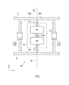
- FIG. 18 is a block diagram illustrating a configuration of an electronic device 1 incorporating the switching converter 2 .
- the electronic device 1 is, for example, a game console or computer.
- a rectifying circuit 100 rectifies and smooths a commercial AC voltage V AC , thus generating a DC voltage V DC .
- An insulating DC/DC converter 102 steps down the DC voltage V DC , thus generating an input voltage V IN .
- the switching converter 2 a DC/DC converter, steps down the input voltage V IN , thus supplying an output voltage V OUT to a load such as a power terminal of a processor 104 .
- Input capacitor C 2 . . . Output capacitor, 20 . . . Controller, M 1 . . . High-side transistor, M 2 . . . Low-side transistor, 30 . . . Circuit board, 32 . . . Axis of symmetry.
- the present invention is applicable to switching converters.
Landscapes
- Engineering & Computer Science (AREA)
- Power Engineering (AREA)
- Physics & Mathematics (AREA)
- Electromagnetism (AREA)
- Microelectronics & Electronic Packaging (AREA)
- Dc-Dc Converters (AREA)
Applications Claiming Priority (3)
| Application Number | Priority Date | Filing Date | Title |
|---|---|---|---|
| JP2014-111670 | 2014-05-29 | ||
| JP2014111670A JP6106127B2 (ja) | 2014-05-29 | 2014-05-29 | スイッチングコンバータおよびそれを用いた電子機器 |
| PCT/JP2015/055415 WO2015182192A1 (ja) | 2014-05-29 | 2015-02-25 | スイッチングコンバータおよびそれを用いた電子機器 |
Publications (2)
| Publication Number | Publication Date |
|---|---|
| US20170093285A1 US20170093285A1 (en) | 2017-03-30 |
| US10027228B2 true US10027228B2 (en) | 2018-07-17 |
Family
ID=54698534
Family Applications (1)
| Application Number | Title | Priority Date | Filing Date |
|---|---|---|---|
| US15/311,316 Active US10027228B2 (en) | 2014-05-29 | 2015-02-25 | Switching converter having noise cancellation feature and electronic device using the same |
Country Status (5)
| Country | Link |
|---|---|
| US (1) | US10027228B2 (enExample) |
| EP (1) | EP3151406B1 (enExample) |
| JP (1) | JP6106127B2 (enExample) |
| CN (1) | CN106464137B (enExample) |
| WO (1) | WO2015182192A1 (enExample) |
Cited By (1)
| Publication number | Priority date | Publication date | Assignee | Title |
|---|---|---|---|---|
| US11037883B2 (en) | 2018-11-16 | 2021-06-15 | Analog Devices International Unlimited Company | Regulator circuit package techniques |
Families Citing this family (20)
| Publication number | Priority date | Publication date | Assignee | Title |
|---|---|---|---|---|
| JP6011736B1 (ja) * | 2016-03-14 | 2016-10-19 | 富士電機株式会社 | 昇圧チョッパ回路 |
| JP6011737B1 (ja) | 2016-03-14 | 2016-10-19 | 富士電機株式会社 | 降圧チョッパ回路 |
| WO2017163481A1 (ja) * | 2016-03-23 | 2017-09-28 | 三菱電機株式会社 | Dc-dcコンバータ |
| EP3361836B1 (de) * | 2017-02-08 | 2020-06-17 | Siemens Aktiengesellschaft | Niederinduktive halbbrückenanordnung |
| DE102017203420A1 (de) * | 2017-03-02 | 2018-09-06 | Siemens Aktiengesellschaft | Halbbrücke für leistungselektronische Schaltungen |
| US10811976B2 (en) | 2017-06-21 | 2020-10-20 | Sumitomo Electric Industries, Ltd. | Electronic circuit device |
| WO2019092926A1 (ja) * | 2017-11-08 | 2019-05-16 | 住友電気工業株式会社 | 電子回路装置 |
| DE102018206291A1 (de) * | 2018-04-24 | 2019-10-24 | Zf Friedrichshafen Ag | EMV-Filter |
| JP6509414B1 (ja) * | 2018-07-30 | 2019-05-08 | 三菱電機株式会社 | 電力変換装置 |
| AU2019335065B2 (en) * | 2018-09-03 | 2024-07-18 | Milspec Technologies Pty Ltd | A DC to DC converter for a vehicle alternator |
| JP7250474B2 (ja) * | 2018-10-19 | 2023-04-03 | 株式会社ソニー・インタラクティブエンタテインメント | 電源装置 |
| JP6835788B2 (ja) | 2018-10-19 | 2021-02-24 | 株式会社ソニー・インタラクティブエンタテインメント | 電源装置 |
| JP7318509B2 (ja) * | 2019-11-29 | 2023-08-01 | 住友電気工業株式会社 | スイッチング回路並びにそれを用いた電力変換装置及び蓄電システム |
| US12316232B2 (en) * | 2020-01-14 | 2025-05-27 | Panasonic Intellectual Property Management Co., Ltd. | Power supply device, ACF converter, and AC adapter |
| CN114285263B (zh) * | 2020-09-28 | 2026-02-10 | 中兴通讯股份有限公司 | 多路开关电源及电子设备 |
| CN112510988A (zh) * | 2020-11-06 | 2021-03-16 | 苏州浪潮智能科技有限公司 | 一种抗电磁干扰的电源电路及其运作方法 |
| CN113422508A (zh) * | 2021-07-12 | 2021-09-21 | 西安超越申泰信息科技有限公司 | 一种降低板级dc-dc开关电源高频噪声的方法 |
| TWI825986B (zh) * | 2021-09-13 | 2023-12-11 | 美商高效電源轉換公司 | 用於具並聯開關之半橋切換電路之電路板布局 |
| CN116137490A (zh) * | 2021-11-18 | 2023-05-19 | 台达电子企业管理(上海)有限公司 | 开关模块 |
| CN119945412A (zh) * | 2024-12-31 | 2025-05-06 | 锐石创芯(深圳)半导体有限公司 | 射频开关、射频芯片及射频前端模组 |
Citations (10)
| Publication number | Priority date | Publication date | Assignee | Title |
|---|---|---|---|---|
| JP2009177998A (ja) | 2008-01-28 | 2009-08-06 | Denso Corp | 車載用電子制御装置 |
| WO2010029917A1 (ja) | 2008-09-09 | 2010-03-18 | トヨタ自動車株式会社 | 電圧変換装置及び電気負荷駆動装置 |
| JP2011259622A (ja) | 2010-06-09 | 2011-12-22 | Denso Corp | 半導体装置 |
| US20130049730A1 (en) | 2011-08-25 | 2013-02-28 | Murata Manufacturing Co., Ltd. | Dc-dc converter |
| WO2013037989A1 (en) | 2011-09-16 | 2013-03-21 | Sma Solar Technology Ag | Circuitry arrangement for reducing a tendency towards oscillations |
| US20140066834A1 (en) | 2012-09-06 | 2014-03-06 | Seiko Epson Corporation | Medical instrument |
| JP2014053742A (ja) | 2012-09-06 | 2014-03-20 | Seiko Epson Corp | スイッチング回路及び医療機器 |
| US20140111174A1 (en) | 2012-10-19 | 2014-04-24 | Linear Technology Corporation | Magnetic Field Cancellation in Switching Regulators |
| US20140117495A1 (en) * | 2012-10-31 | 2014-05-01 | Delta Electronics (Shanghai) Co., Ltd. | Switch circuit package module |
| US20140183550A1 (en) * | 2012-12-31 | 2014-07-03 | Efficient Power Conversion Corporation | Parasitic inductance reduction for multilayered board layout designs with semiconductor devices |
Family Cites Families (5)
| Publication number | Priority date | Publication date | Assignee | Title |
|---|---|---|---|---|
| US4959764A (en) * | 1989-11-14 | 1990-09-25 | Computer Products, Inc. | DC/DC converter switching at zero voltage |
| DE69501931T2 (de) * | 1994-09-16 | 1998-09-10 | Toshiba Kawasaki Kk | Micro-Leistungsversorgung mit einem Schalelement |
| EP2122827B1 (en) * | 2007-03-13 | 2013-05-29 | Telefonaktiebolaget LM Ericsson (publ) | Flexible dynamic range amplifier |
| JP2013017310A (ja) * | 2011-07-04 | 2013-01-24 | Sumitomo Heavy Ind Ltd | 電力変換装置 |
| US20140103909A1 (en) * | 2012-10-17 | 2014-04-17 | System General Corp. | Method and apparatus for detecting position and startup a sensorless motor |
-
2014
- 2014-05-29 JP JP2014111670A patent/JP6106127B2/ja active Active
-
2015
- 2015-02-25 WO PCT/JP2015/055415 patent/WO2015182192A1/ja not_active Ceased
- 2015-02-25 EP EP15798727.2A patent/EP3151406B1/en active Active
- 2015-02-25 US US15/311,316 patent/US10027228B2/en active Active
- 2015-02-25 CN CN201580026723.1A patent/CN106464137B/zh active Active
Patent Citations (16)
| Publication number | Priority date | Publication date | Assignee | Title |
|---|---|---|---|---|
| JP2009177998A (ja) | 2008-01-28 | 2009-08-06 | Denso Corp | 車載用電子制御装置 |
| WO2010029917A1 (ja) | 2008-09-09 | 2010-03-18 | トヨタ自動車株式会社 | 電圧変換装置及び電気負荷駆動装置 |
| US20110148370A1 (en) | 2008-09-09 | 2011-06-23 | Koichi Mizutani | Voltage conversion apparatus and electrical load driving apparatus |
| US9088202B2 (en) | 2008-09-09 | 2015-07-21 | Toyota Jidosha Kabushiki Kaisha | Voltage conversion apparatus and electrical load driving apparatus to reduce noise through magnetic field |
| JP2011259622A (ja) | 2010-06-09 | 2011-12-22 | Denso Corp | 半導体装置 |
| US8811027B2 (en) | 2011-08-25 | 2014-08-19 | Murata Manufacturing Co., Ltd. | DC-DC converter |
| US20130049730A1 (en) | 2011-08-25 | 2013-02-28 | Murata Manufacturing Co., Ltd. | Dc-dc converter |
| JP2013046509A (ja) | 2011-08-25 | 2013-03-04 | Murata Mfg Co Ltd | Dc−dcコンバータ |
| WO2013037989A1 (en) | 2011-09-16 | 2013-03-21 | Sma Solar Technology Ag | Circuitry arrangement for reducing a tendency towards oscillations |
| JP2014053742A (ja) | 2012-09-06 | 2014-03-20 | Seiko Epson Corp | スイッチング回路及び医療機器 |
| US20140066834A1 (en) | 2012-09-06 | 2014-03-06 | Seiko Epson Corporation | Medical instrument |
| JP2014087252A (ja) | 2012-10-19 | 2014-05-12 | Linear Technol Corp | スイッチングレギュレータにおける磁場キャンセル |
| US20140111174A1 (en) | 2012-10-19 | 2014-04-24 | Linear Technology Corporation | Magnetic Field Cancellation in Switching Regulators |
| US8823345B2 (en) | 2012-10-19 | 2014-09-02 | Linear Technology Corporation | Magnetic field cancellation in switching regulators |
| US20140117495A1 (en) * | 2012-10-31 | 2014-05-01 | Delta Electronics (Shanghai) Co., Ltd. | Switch circuit package module |
| US20140183550A1 (en) * | 2012-12-31 | 2014-07-03 | Efficient Power Conversion Corporation | Parasitic inductance reduction for multilayered board layout designs with semiconductor devices |
Non-Patent Citations (3)
| Title |
|---|
| European Search Report for corresponding EP Application No. 15798727.2, 9 pages, dated Dec. 11, 2017. |
| International Preliminary Report and Written Search Report for corresponding PCT Application No. PCT/JP2015/055415, 15 pages, dated Dec. 8, 2016. |
| International Searc Report for corresponding PCT Application No. PCT/JP2015/055415, 4 pages, dated May 19, 2015. |
Cited By (4)
| Publication number | Priority date | Publication date | Assignee | Title |
|---|---|---|---|---|
| US11037883B2 (en) | 2018-11-16 | 2021-06-15 | Analog Devices International Unlimited Company | Regulator circuit package techniques |
| US20210257313A1 (en) * | 2018-11-16 | 2021-08-19 | Analog Devices International Unlimited Company | Regulator circuit package techniques |
| US11955437B2 (en) * | 2018-11-16 | 2024-04-09 | Analog Devices International Unlimited Company | Regulator circuit package techniques |
| US12550742B2 (en) * | 2018-11-16 | 2026-02-10 | Analog Devices International Unlimited Company | Regulator circuit package techniques |
Also Published As
| Publication number | Publication date |
|---|---|
| EP3151406A4 (en) | 2018-01-10 |
| EP3151406A1 (en) | 2017-04-05 |
| WO2015182192A1 (ja) | 2015-12-03 |
| JP2015226438A (ja) | 2015-12-14 |
| CN106464137A (zh) | 2017-02-22 |
| EP3151406B1 (en) | 2020-11-18 |
| JP6106127B2 (ja) | 2017-03-29 |
| CN106464137B (zh) | 2020-02-21 |
| US20170093285A1 (en) | 2017-03-30 |
Similar Documents
| Publication | Publication Date | Title |
|---|---|---|
| US10027228B2 (en) | Switching converter having noise cancellation feature and electronic device using the same | |
| EP2722987B1 (en) | Magnetic field cancellation in switching regulators | |
| JP6371309B2 (ja) | 多層化された半導体素子のための寄生インダクタンス削減回路基板レイアウト設計 | |
| US10667383B2 (en) | Printed circuit board and switching power supply for electronic appliance | |
| US10620654B2 (en) | Alternatingly-switched parallel circuit, integrated power module and integrated power package | |
| CN113950727A (zh) | 堆叠矩阵变压器 | |
| EP2744093A1 (en) | Power supply device | |
| US11387761B2 (en) | System and method for sinusoidal output and integrated EMC filtering in a motor drive | |
| US20200195123A1 (en) | Alternatingly-switched parallel circuit, integrated power module and integrated power package | |
| US9041460B2 (en) | Packaged power transistors and power packages | |
| Blecic et al. | EMC-oriented design of output stage of synchronous buck converter | |
| US20260031717A1 (en) | Multi-phase power converter circuit layout to minimize drive loop and power loop inductances | |
| US9584010B2 (en) | Power supply apparatus | |
| CN102257712A (zh) | 电压转换装置和电气负载驱动装置 | |
| JP2006280148A (ja) | 電圧制御装置 | |
| US11271489B2 (en) | AC-DC power supply and motor | |
| CN117097148A (zh) | Llc变换器、电源模块和充电装置 | |
| Waghela et al. | Switched-mode power supply design guidelines for smartphones and tablets for reducing rf emissions | |
| CN122001199A (zh) | 电源中的泄漏电流补偿 | |
| JP2015201965A (ja) | 電源装置 | |
| JP2006174527A (ja) | 電力変換器 |
Legal Events
| Date | Code | Title | Description |
|---|---|---|---|
| AS | Assignment |
Owner name: SONY INTERACTIVE ENTERTAINMENT INC., JAPAN Free format text: ASSIGNMENT OF ASSIGNORS INTEREST;ASSIGNOR:SASAO, KAZUKI;REEL/FRAME:040327/0742 Effective date: 20160926 |
|
| STCF | Information on status: patent grant |
Free format text: PATENTED CASE |
|
| MAFP | Maintenance fee payment |
Free format text: PAYMENT OF MAINTENANCE FEE, 4TH YEAR, LARGE ENTITY (ORIGINAL EVENT CODE: M1551); ENTITY STATUS OF PATENT OWNER: LARGE ENTITY Year of fee payment: 4 |
|
| MAFP | Maintenance fee payment |
Free format text: PAYMENT OF MAINTENANCE FEE, 8TH YEAR, LARGE ENTITY (ORIGINAL EVENT CODE: M1552); ENTITY STATUS OF PATENT OWNER: LARGE ENTITY Year of fee payment: 8 |