EP3151406B1 - Switching converter and electronic device using same - Google Patents
Switching converter and electronic device using same Download PDFInfo
- Publication number
- EP3151406B1 EP3151406B1 EP15798727.2A EP15798727A EP3151406B1 EP 3151406 B1 EP3151406 B1 EP 3151406B1 EP 15798727 A EP15798727 A EP 15798727A EP 3151406 B1 EP3151406 B1 EP 3151406B1
- Authority
- EP
- European Patent Office
- Prior art keywords
- transistor
- transistors
- switching
- switching converter
- smoothing circuit
- Prior art date
- Legal status (The legal status is an assumption and is not a legal conclusion. Google has not performed a legal analysis and makes no representation as to the accuracy of the status listed.)
- Active
Links
Images


Classifications
-
- H—ELECTRICITY
- H02—GENERATION; CONVERSION OR DISTRIBUTION OF ELECTRIC POWER
- H02M—APPARATUS FOR CONVERSION BETWEEN AC AND AC, BETWEEN AC AND DC, OR BETWEEN DC AND DC, AND FOR USE WITH MAINS OR SIMILAR POWER SUPPLY SYSTEMS; CONVERSION OF DC OR AC INPUT POWER INTO SURGE OUTPUT POWER; CONTROL OR REGULATION THEREOF
- H02M3/00—Conversion of dc power input into dc power output
- H02M3/02—Conversion of dc power input into dc power output without intermediate conversion into ac
- H02M3/04—Conversion of dc power input into dc power output without intermediate conversion into ac by static converters
- H02M3/10—Conversion of dc power input into dc power output without intermediate conversion into ac by static converters using discharge tubes with control electrode or semiconductor devices with control electrode
- H02M3/145—Conversion of dc power input into dc power output without intermediate conversion into ac by static converters using discharge tubes with control electrode or semiconductor devices with control electrode using devices of a triode or transistor type requiring continuous application of a control signal
- H02M3/155—Conversion of dc power input into dc power output without intermediate conversion into ac by static converters using discharge tubes with control electrode or semiconductor devices with control electrode using devices of a triode or transistor type requiring continuous application of a control signal using semiconductor devices only
- H02M3/156—Conversion of dc power input into dc power output without intermediate conversion into ac by static converters using discharge tubes with control electrode or semiconductor devices with control electrode using devices of a triode or transistor type requiring continuous application of a control signal using semiconductor devices only with automatic control of output voltage or current, e.g. switching regulators
- H02M3/158—Conversion of dc power input into dc power output without intermediate conversion into ac by static converters using discharge tubes with control electrode or semiconductor devices with control electrode using devices of a triode or transistor type requiring continuous application of a control signal using semiconductor devices only with automatic control of output voltage or current, e.g. switching regulators including plural semiconductor devices as final control devices for a single load
-
- H—ELECTRICITY
- H02—GENERATION; CONVERSION OR DISTRIBUTION OF ELECTRIC POWER
- H02M—APPARATUS FOR CONVERSION BETWEEN AC AND AC, BETWEEN AC AND DC, OR BETWEEN DC AND DC, AND FOR USE WITH MAINS OR SIMILAR POWER SUPPLY SYSTEMS; CONVERSION OF DC OR AC INPUT POWER INTO SURGE OUTPUT POWER; CONTROL OR REGULATION THEREOF
- H02M1/00—Details of apparatus for conversion
- H02M1/44—Circuits or arrangements for compensating for electromagnetic interference in converters or inverters
-
- H—ELECTRICITY
- H02—GENERATION; CONVERSION OR DISTRIBUTION OF ELECTRIC POWER
- H02M—APPARATUS FOR CONVERSION BETWEEN AC AND AC, BETWEEN AC AND DC, OR BETWEEN DC AND DC, AND FOR USE WITH MAINS OR SIMILAR POWER SUPPLY SYSTEMS; CONVERSION OF DC OR AC INPUT POWER INTO SURGE OUTPUT POWER; CONTROL OR REGULATION THEREOF
- H02M3/00—Conversion of dc power input into dc power output
- H02M3/02—Conversion of dc power input into dc power output without intermediate conversion into ac
- H02M3/04—Conversion of dc power input into dc power output without intermediate conversion into ac by static converters
- H02M3/10—Conversion of dc power input into dc power output without intermediate conversion into ac by static converters using discharge tubes with control electrode or semiconductor devices with control electrode
- H02M3/145—Conversion of dc power input into dc power output without intermediate conversion into ac by static converters using discharge tubes with control electrode or semiconductor devices with control electrode using devices of a triode or transistor type requiring continuous application of a control signal
- H02M3/155—Conversion of dc power input into dc power output without intermediate conversion into ac by static converters using discharge tubes with control electrode or semiconductor devices with control electrode using devices of a triode or transistor type requiring continuous application of a control signal using semiconductor devices only
-
- H—ELECTRICITY
- H05—ELECTRIC TECHNIQUES NOT OTHERWISE PROVIDED FOR
- H05K—PRINTED CIRCUITS; CASINGS OR CONSTRUCTIONAL DETAILS OF ELECTRIC APPARATUS; MANUFACTURE OF ASSEMBLAGES OF ELECTRICAL COMPONENTS
- H05K1/00—Printed circuits
- H05K1/02—Details
- H05K1/0213—Electrical arrangements not otherwise provided for
- H05K1/0216—Reduction of cross-talk, noise or electromagnetic interference
- H05K1/0228—Compensation of cross-talk by a mutually correlated lay-out of printed circuit traces, e.g. for compensation of cross-talk in mounted connectors
-
- H—ELECTRICITY
- H02—GENERATION; CONVERSION OR DISTRIBUTION OF ELECTRIC POWER
- H02M—APPARATUS FOR CONVERSION BETWEEN AC AND AC, BETWEEN AC AND DC, OR BETWEEN DC AND DC, AND FOR USE WITH MAINS OR SIMILAR POWER SUPPLY SYSTEMS; CONVERSION OF DC OR AC INPUT POWER INTO SURGE OUTPUT POWER; CONTROL OR REGULATION THEREOF
- H02M3/00—Conversion of dc power input into dc power output
- H02M3/003—Constructional details, e.g. physical layout, assembly, wiring or busbar connections
-
- H—ELECTRICITY
- H02—GENERATION; CONVERSION OR DISTRIBUTION OF ELECTRIC POWER
- H02M—APPARATUS FOR CONVERSION BETWEEN AC AND AC, BETWEEN AC AND DC, OR BETWEEN DC AND DC, AND FOR USE WITH MAINS OR SIMILAR POWER SUPPLY SYSTEMS; CONVERSION OF DC OR AC INPUT POWER INTO SURGE OUTPUT POWER; CONTROL OR REGULATION THEREOF
- H02M7/00—Conversion of ac power input into dc power output; Conversion of dc power input into ac power output
- H02M7/003—Constructional details, e.g. physical layout, assembly, wiring or busbar connections
-
- H—ELECTRICITY
- H05—ELECTRIC TECHNIQUES NOT OTHERWISE PROVIDED FOR
- H05K—PRINTED CIRCUITS; CASINGS OR CONSTRUCTIONAL DETAILS OF ELECTRIC APPARATUS; MANUFACTURE OF ASSEMBLAGES OF ELECTRICAL COMPONENTS
- H05K1/00—Printed circuits
- H05K1/02—Details
- H05K1/0213—Electrical arrangements not otherwise provided for
- H05K1/0216—Reduction of cross-talk, noise or electromagnetic interference
- H05K1/023—Reduction of cross-talk, noise or electromagnetic interference using auxiliary mounted passive components or auxiliary substances
- H05K1/0231—Capacitors or dielectric substances
Definitions
- the present invention relates to a switching converter having switching elements.
- DC/DC converters switching regulators
- AC/DC converters AC/DC converters
- DC/DC converters switching regulators
- AC/DC converters AC/DC converters
- DC/DC converters are designed to step down a direct current (DC) voltage supplied from a battery or inverter to an optimal voltage level for load.
- AC/DC converters are designed to convert an alternating current (AC) voltage into a corresponding DC voltage.
- FIG. 1 is a circuit diagram illustrating a configuration example of a switching converter 2r studied by the present inventors.
- the switching converter 2r illustrated in FIG. 1 is a step-down DC/DC converter and primarily includes an output circuit 10 and a control circuit (controller) 20.
- the switching converter 2r steps down an input voltage V IN of an input line 4 to a given level, supplying an output voltage V OUT to a load (not shown) connected to an output line 8.
- the output circuit 10 includes an input capacitor C1, an output capacitor C2, a high-side transistor (switching transistor) M1, a low-side transistor (synchronous rectification transistor) M2, and an inductor L1.
- the input capacitor C1 is provided between the input line 4 and a ground line 6 to stabilize the input voltage V IN .
- the output capacitor C2 is connected between the output line 8 and the ground line 6 to smooth the output voltage V OUT .
- the high-side transistor M1 and the low-side transistor M2 are connected in series between the input line 4 and the ground line 6, i.e., in parallel with the input capacitor C1.
- the inductor L1 is provided between a switching node (or also referred to as a switching line) 9 and the output line 8.
- the switching node is a connection point between the high-side transistor M1 and the low-side transistor M2.
- the controller 20 is supplied with a feedback voltage V FB that is proportional to the output voltage V OUT .
- the controller 20 generates a pulse signal whose duty ratio is adjusted so that the feedback voltage V FB approaches a given reference voltage V REF .
- the controller 20 generates a gate voltage HG for the high-side transistor M1 and a gate voltage LG for the low-side transistor M2 in accordance with the pulse signal, complementarily switching between the high-side transistor M1 and the low-side transistor M2 with a dead time provided between the switching events. Switching between the high-side transistor M1 and the low-side transistor M2 is controlled by the controller 20, stabilizing the output voltage V OUT to a target level.
- EP 2722987 A1 discloses switching regulators which comprise at least three switches and at least two capacitors arranged symmetrically.
- the present inventor has recognized the following problem as a result of study of the switching converter 2r illustrated in FIG. 1 .
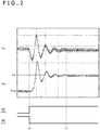
- FIG. 2 is an operation waveform diagram of the switching converter 2r illustrated in FIG. 1 .
- FIG. 2 shows the input voltage V IN and a voltage (referred to as a switching voltage) V SW of the switching node 9.
- V IN input voltage
- V SW switching voltage
- the gate voltages HG and LG are at low and high levels, respectively, with the high-side transistor M1 and the low-side transistor M2 being OFF and ON, respectively.
- the gate voltage HG of the high-side transistor M1 goes up to high level, and the gate voltage LG of the low-side transistor M2 goes down to low level.
- the high-side transistor M1 turns fully ON and remains ON, and the low-side transistor M2 turns OFF, causing the switching voltage V SW to be substantially equal to the input voltage V IN .
- switching between the high-side transistor M1 and the low-side transistor M2 is controlled in such a manner that a dead time is provided between the switching events. However, such a dead time is ignored here.
- the switching converter 2r illustrated in FIG. 1 has a current loop that includes the input capacitor C1, the output capacitor C2, the high-side transistor M1, and the low-side transistor M2.
- a current including high-frequency components resulting from switching between the high-side transistor M1 and the low-side transistor M2 flows into the current loop including the input capacitor C1, the high-side transistor M1, and the low-side transistor M2, thus resulting in ringing of the input voltage V IN and the switching voltage V SW .
- the ringing frequency is often about several tens to hundreds of MHz, for example.
- the present invention has been devised in light of the foregoing, and it is an illustrative object of a mode of the present invention to provide a switching converter that contributes to reduce EMI.
- a mode of the present invention relates to a switching converter.
- the switching converter includes a smoothing circuit and first and second transistors.
- the smoothing circuit includes at least one capacitor.
- the first and second transistors are connected in series between two ends of the smoothing circuit.
- the first and second transistors are arranged side by side in a first direction on a circuit board.
- Two current loops that run through the smoothing circuit and the first and second transistors are formed to be substantially linearly symmetrical with respect to an axis of symmetry that extends in the first direction.
- Another mode of the present invention relates to an electronic device.
- the electronic device includes one of the above switching converters.
- the present invention contributes to reduce EMI of switching converters.
- the expression "the condition in which a member A is connected to a member B" includes not only physical and direct connection of the member A to the member B but also indirect connection of the members A and B via other member that does not affect the electrical connection condition.
- the expression "the condition in which a member C is provided between the members A and B" includes not only direct connection of the members A and C or the members B and C but also indirect connection of the members A and C or the members B and C via other member that does not affect the electrical connection condition.
- FIG. 3 is a circuit diagram of a switching converter 2 according to a first embodiment.
- the switching converter 2 is similar in basic configuration to its counterpart shown in FIG. 1 .
- an even number of input capacitors such as two input capacitors C1a and C1b are connected in parallel between the input line 4 and the ground line 6.
- the input capacitors C1a and C1b are referred to as an input smoothing circuit 12.
- the high-side transistor (first transistor) M1 and the low-side transistor (second transistor) M2 may be packaged in a single power module 14 as illustrated in FIG. 3 .
- the power module 14 includes a drain terminal P1, a source terminal P2, a switching terminal P3, and a first gate terminal P4, and a second gate terminal P5.
- the drain terminal P1 is connected to one end (drain) of the high-side transistor M1.
- the source terminal P2 is connected to one end (source) of the low-side transistor M2.
- the switching terminal P3 is connected to a switching terminal, a connection node between the high-side transistor M1 and the low-side transistor M2.
- the drain terminal P1 is connected to the input line 4.
- the source terminal P2 is connected to the ground line 6.
- the switching terminal P3 is connected to the inductor L1 via a switching line 9.
- Gate drive voltages HG and LG from the controller 20 are fed to the first and second gate terminals P4 and P5, respectively.
- the high-side transistor M1 may be a P-channel MOSFET.
- an insulated gate bipolar transistor (IGBT) or a bipolar transistor may be used rather than a MOSFET.
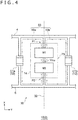
- FIG. 4 is a basic layout diagram of the switching converter 2 illustrated in FIG. 3 . It should be noted that only part of the output circuit 10 of the switching converter 2 is shown here for simple description and easy understanding.
- the high-side transistor M1 and the low-side transistor M2 are arranged side by side in a first direction (X direction) on a circuit board 30. Then, a current loop 50 that runs through the smoothing circuit 12, the high-side transistor M1, and the low-side transistor M2 branches into two current loops 50a and 50b. These loops are formed to be substantially linearly symmetrical with respect to an axis of symmetry 32 that extends in the first direction (X direction).
- the input line 4 and the ground line 6 are formed as printed circuits on the circuit board 30.
- the input smoothing circuit 12 includes the two capacitors C1a and C1b.
- the two capacitors C1a and C1b are arranged symmetrically with the mounting area of the high-side transistor M1 and the low-side transistor M2, in other words, the mounting area of the power module 14, provided therebetween.
- the wiring pattern (layout) of the input line 4 and the ground line 6 is designed so that the first and second current loops 50a and 50b are linearly symmetrical with respect to the axis of symmetry 32.
- the first current loop 50a runs through the one capacitor C1a, the high-side transistor M1, and the low-side transistor M2.
- the second current loop 50b runs through the other capacitor C1b, the high-side transistor M1, and the low-side transistor M2.
- FIG. 5 is a diagram illustrating the operating principle of the switching converter 2 according to the first embodiment. Because of the symmetrical layout, currents flow in opposite directions in the first and second current loops 50a and 50b. As a result, magnetic flux densities Ba and Bb induced by the currents flowing through each of the current loops 50a and 50b are opposite in direction.
- the magnetic flux densities Ba and Bb cancel out at an arbitrary point near the power module 14, thus contributing to reduce electromagnetic noise or EMI as compared to formation of a single current loop.
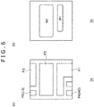
- FIG. 6(a) is a diagram illustrating a pin assignment of the power module 14, and FIG. 6(b) is a diagram illustrating an internal layout thereof.
- the high-side transistor M1 and the low-side transistor M2 are arranged side by side in the first direction (X direction) inside the power module 14.
- the high-side transistor M1 and the low-side transistor M2 may be integrated in a single die (chip) or may be individually integrated in two separate dies.
- drain terminal P1, the source terminal P2, and the switching terminal P3 are arranged in the first direction (X direction).
- the drain terminal P1 and the source terminal P2 may be interchanged.
- asymmetrical dual N-channel MOSFET FDPC8016S
- Fairchild asymmetrical dual N-channel MOSFET
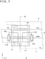
- FIG. 7 is a specific layout diagram of the switching converter 2 illustrated in FIG. 3 .
- the power module 14 having the pin assignment shown in FIG. 6(a) is used.
- Each of the input line 4 and the ground line 6 has a portion that extends in a second direction (Y direction) perpendicular to the first direction (X direction) near the mounting areas of the input smoothing circuit 12 and the power module 14. More specifically, the input line 4 and the ground line 6 are formed to overlap the drain terminal P1 and the source terminal P2, respectively.
- the switching line 9 may be formed in parallel with the input line 4 and the ground line 6 in such a manner as to overlap the switching terminal P3.
- the input capacitors C1a and C1b are arranged side by side in the Y direction in such a manner as to sandwich the power module 14. One end of each of the input capacitors C1a and C1b is connected to the input line 4, with the other end thereof connected to the ground line 6.
- the two current loops 50a and 50b are formed that are substantially linearly symmetrical about the axis of symmetry 32. As described with reference to FIG. 5 , therefore, the magnetic fluxes generated by the two current loops 50a and 50b cancel each other out, thus contributing to reduce EMI.
- FIG. 8 is a layout diagram of the switching converter 2r according to a comparative technology.
- the input smoothing circuit 12 includes two input capacitors C1b and C1c that are arranged adjacent to each other. In this case, two current loops 50b and 50c are formed to substantially overlap each other and interlink with a common magnetic flux.
- the current loop 50b runs through the input capacitor C1b and the transistors M1 and M2.
- the current loop 50c runs through the input capacitor C1c and the transistors M1 and M2.
- FIGS. 9(a) and 9(b) are diagrams illustrating measurement results of magnetic fields near the switching converters 2 and 2r illustrated respectively in FIGS. 7 and 8 .
- the magnetic fields were measured 10 mm away from the surface of the power module 14 using a near magnetic field tester (EMI tester: Peritec's EMV-200).
- EMI tester Peritec's EMV-200
- an improvement of about 1.3 dB is observed in the layout shown in FIG. 7 over the layout shown in FIG. 8 .
- FIGS. 10(a) and 10(b) are diagrams illustrating calculation results of magnetic fields near the switching converters 2r and 2 illustrated respectively in FIGS. 8 and 7 .
- the measured points were positioned 10 mm away from the surface of the power module 14. As is clear from the simulation results, an improvement of up to 7.4 dB is observed by arranging the two current loops symmetrically if the magnetic flux Bz in the Z direction is considered.
- (i) is a curve for the layout shown in FIG. 7
- a closed loop formed by a smoothing circuit and two transistors branches into two loops.
- the smoothing circuit includes capacitors.
- the two transistors are connected in series between the two ends of the smoothing circuit.
- the two loops are laid out in a linearly symmetrical manner. This layout contributes to reduce EMI.
- the following advantage can be obtained by using the power module 14 whose drain terminal P1 and source terminal P2 are arranged adjacent to each other as illustrated in FIG. 6(a) as compared to the layout illustrated in FIG. 4 .
- the drain terminal P1 and the source terminal P2 are not adjacent to each other, with the switching terminal P3 arranged at the center.
- the switching line 9 to be connected to the switching terminal P3 must straddle the input line 4 or the ground line 6. In order to do so, it is necessary to form part of wiring on the rear face of the circuit board 30 and connect the switching line 9 to the switching terminal P3 by means of via holes.
- via holes are not preferred because they lead to a difficult-to-predict parasitic inductance.
- drain terminal P1 and the source terminal P2 adjacent to each other contributes to a smaller current loop area, in other words, smaller impedance within the current loop, thus reducing power noise accompanied by high-frequency ringing and cutting down the absolute value of EMI.
- FIG. 12 is a circuit diagram of a switching converter 2a according to a second embodiment.
- the switching converter 2a is similar in basic configuration to its counterpart shown in FIG. 3 .
- a plurality of N, and specifically an even number of, and more specifically two, power modules 14a and 14b are connected in parallel between the input line 4 and the ground line 6.
- the high-side transistor M1 includes two transistors M1a and M1b that are connected in parallel
- the low-side transistor M2 includes two transistors M2a and M2b that are connected in parallel.
- FIG. 13 is a layout diagram of the switching converter 2a illustrated in FIG. 12 .
- the input smoothing circuit 12 including the input capacitor C1 is arranged on the axis of symmetry 32, and the two power modules 14a and 14b are arranged to be linearly symmetrical with respect to the axis of symmetry 32 in such a manner as to sandwich the input smoothing circuit 12.
- the two transistors (not shown) inside the power module 14a are arranged side by side in the X direction.
- the two transistors (not shown) inside the power module 14b are arranged side by side in the X direction.
- the input smoothing circuit 12 may include the plurality of input capacitors C1 as in FIG. 3 . In this case, it is only necessary to arrange the plurality of input capacitors C1 adjacent to each other in the first direction (Y direction).
- the two current loops 50a and 50b are also formed that are substantially linearly symmetrical about the axis of symmetry 32. As described with reference to FIG. 5 , therefore, the magnetic fluxes generated by the two current loops 50a and 50b cancel each other out, thus contributing to reduce EMI.
- the high-side transistor (first transistor) M1 and the low-side transistor (second transistor) M2 are packaged in a single power module.
- the present invention is not limited thereto. That is, the high-side transistor M1 and the low-side transistor M2 may be discrete elements that are packaged separately.
- FIGS. 14(a) and 14(b) are, respectively, a circuit diagram and a layout diagram of a switching converter 2e according to a first modification example.
- the equivalent circuit is similar to that shown in FIG. 12 except that the transistors M1a and M2a of the power module 14a and the transistors M1b and M2b of the power module 14b are separate elements.
- FIGS. 15(a) and 15(b) are layout diagrams of switching converters 2f and 2g according to a second modification example.
- the switching converter 2f illustrated in FIG. 15(a) uses the two power modules 14a and 14b whose pin assignments are bilaterally symmetrical in the switching converter 2a illustrated in FIG. 13 .
- the input smoothing circuit 12 includes the input capacitor C1. It should be noted that the input smoothing circuit 12 may include a plurality of input capacitors arranged side by side in the first direction in the present modification example.
- the switching converter 2g illustrated in FIG. 15(b) uses the discrete elements M1a and M1b, and M2a and M2b whose pin assignments are bilaterally symmetrical in the switching converter 2e illustrated in FIG. 14(b) .
- using the elements with bilaterally symmetrical pin assignments provides further enhanced symmetry between the two current loops, thus contributing to further reduced EMI.
- having bilaterally symmetrical pin assignments contributes to an even smaller current loop area, in other words, smaller impedance within the current loops, thus reducing power noise accompanied by high-frequency ringing and cutting down the absolute value of EMI.
- FIG. 16 is a layout diagram of a switching converter 2h according to a third modification example.
- the first transistor M1 and the second transistor M2 are arranged side by side on a first face of the circuit board.
- the input capacitor C1 of the smoothing circuit 12 is arranged on the axis of symmetry 32 on a second face, the rear side of the first face of the circuit board. Wiring on the first and second faces is electrically connected by means of via holes (through holes) VH.
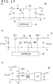
- FIGS. 17(a) to 17(c) are circuit diagrams of modification examples of the switching converter 2.
- a switching converter 2b illustrated in FIG. 17(a) is a step-up DC/DC converter.
- the switching transistor (first transistor) M1 and the synchronous rectification transistor (second transistor) M2 are provided in series between the two ends of an output smoothing circuit 16 that includes the output capacitor C2. Therefore, it is only necessary to lay out the current loop formed by the output smoothing circuit 16 and the transistors M1 and M2 so that the current loop is symmetrical with respect to a given axis of symmetry.
- a switching converter 2c illustrated in FIG. 17(b) is a step-up DC/DC converter.
- the switching converter 2c can be considered a combination of step-down DC/DC converter and step-up DC/DC converter. Therefore, it is possible to provide reduced EMI by forming two current loops in a linearly symmetrical manner, one that runs through the input smoothing circuit 12 and transistors M11 and M12 and another that runs through the output smoothing circuit 16 and transistors M21 and M22.
- a switching converter 2d illustrated in FIG. 17(c) is an insulating switching power supply using a transformer.
- Transistors 31 and 32 form a half-bridge circuit 18.
- the transistors 31 and 32 of the half-bridge circuit 18 are connected in series between the two ends of the input smoothing circuit 12. Therefore, it is only necessary to lay out the current loop formed by the input smoothing circuit 12 and the transistors M31 and M32 so that the current loop is symmetrical with respect to a given axis of symmetry.
- the present invention is applicable to other switching converters such as three-phase inverter.
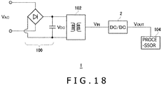
- FIG. 18 is a block diagram illustrating a configuration of an electronic device 1 incorporating the switching converter 2.
- the electronic device 1 is, for example, a game console or computer.
- a rectifying circuit 100 rectifies and smooths a commercial AC voltage V AC , thus generating a DC voltage V DC .
- An insulating DC/DC converter 102 steps down the DC voltage V DC , thus generating an input voltage V IN .
- the switching converter 2, a DC/DC converter, steps down the input voltage V IN , thus supplying an output voltage V OUT to a load such as a power terminal of a processor 104.
- 2...Switching converter 4...Input line, 6...Ground line, 8...Output line, 9...Switching line, 10...Output circuit, 12...Input smoothing circuit, 14...Power module, 16...Output smoothing circuit, 18...Half-bridge circuit, P1...Drain terminal, P2...Source terminal, P3...Switching terminal, P4...First gate terminal, P5...Second gate terminal, L1...Inductor, C1...Input capacitor, C2...Output capacitor, 20...Controller, M1...High-side transistor, M2...Low-side transistor, 30...Circuit board, 32...Axis of symmetry.
- the present invention is applicable to switching converters.
Description
- The present invention relates to a switching converter having switching elements.
- In electronic devices such as personal computers and game consoles, various switching converters are used. Among popular switching converters are DC/DC converters (switching regulators) and AC/DC converters. DC/DC converters are designed to step down a direct current (DC) voltage supplied from a battery or inverter to an optimal voltage level for load. AC/DC converters are designed to convert an alternating current (AC) voltage into a corresponding DC voltage.
-
FIG. 1 is a circuit diagram illustrating a configuration example of aswitching converter 2r studied by the present inventors. Theswitching converter 2r illustrated inFIG. 1 is a step-down DC/DC converter and primarily includes anoutput circuit 10 and a control circuit (controller) 20. - The
switching converter 2r steps down an input voltage VIN of aninput line 4 to a given level, supplying an output voltage VOUT to a load (not shown) connected to anoutput line 8. - The
output circuit 10 includes an input capacitor C1, an output capacitor C2, a high-side transistor (switching transistor) M1, a low-side transistor (synchronous rectification transistor) M2, and an inductor L1. - The input capacitor C1 is provided between the
input line 4 and aground line 6 to stabilize the input voltage VIN. The output capacitor C2 is connected between theoutput line 8 and theground line 6 to smooth the output voltage VOUT. - The high-side transistor M1 and the low-side transistor M2 are connected in series between the
input line 4 and theground line 6, i.e., in parallel with the input capacitor C1. The inductor L1 is provided between a switching node (or also referred to as a switching line) 9 and theoutput line 8. The switching node is a connection point between the high-side transistor M1 and the low-side transistor M2. - The
controller 20 is supplied with a feedback voltage VFB that is proportional to the output voltage VOUT. Thecontroller 20 generates a pulse signal whose duty ratio is adjusted so that the feedback voltage VFB approaches a given reference voltage VREF. Thecontroller 20 generates a gate voltage HG for the high-side transistor M1 and a gate voltage LG for the low-side transistor M2 in accordance with the pulse signal, complementarily switching between the high-side transistor M1 and the low-side transistor M2 with a dead time provided between the switching events. Switching between the high-side transistor M1 and the low-side transistor M2 is controlled by thecontroller 20, stabilizing the output voltage VOUT to a target level. -
EP 2722987 A1 discloses switching regulators which comprise at least three switches and at least two capacitors arranged symmetrically. - The present inventor has recognized the following problem as a result of study of the
switching converter 2r illustrated inFIG. 1 . -
FIG. 2 is an operation waveform diagram of theswitching converter 2r illustrated inFIG. 1 .FIG. 2 shows the input voltage VIN and a voltage (referred to as a switching voltage) VSW of theswitching node 9. Prior to time t0, the gate voltages HG and LG are at low and high levels, respectively, with the high-side transistor M1 and the low-side transistor M2 being OFF and ON, respectively. The switching voltage VSW is at a ground voltage (VGND = 0 V) . - At time t0, the gate voltage HG of the high-side transistor M1 goes up to high level, and the gate voltage LG of the low-side transistor M2 goes down to low level. At time t1, a given transition time later, and beyond, the high-side transistor M1 turns fully ON and remains ON, and the low-side transistor M2 turns OFF, causing the switching voltage VSW to be substantially equal to the input voltage VIN. It should be noted that, in an actual DC/DC converter, switching between the high-side transistor M1 and the low-side transistor M2 is controlled in such a manner that a dead time is provided between the switching events. However, such a dead time is ignored here.
- The
switching converter 2r illustrated inFIG. 1 has a current loop that includes the input capacitor C1, the output capacitor C2, the high-side transistor M1, and the low-side transistor M2. During the transition time from t0 to t1, a current including high-frequency components resulting from switching between the high-side transistor M1 and the low-side transistor M2 flows into the current loop including the input capacitor C1, the high-side transistor M1, and the low-side transistor M2, thus resulting in ringing of the input voltage VIN and the switching voltage VSW. Although dependent on the resonance frequency of the resonance circuit including the inductor L1, the ringing frequency is often about several tens to hundreds of MHz, for example. - Power noise associated with this high-frequency ringing adversely affects other electronic devices as electromagnetic interference (EMI). Therefore, designers of electronic devices end up spending enormous amounts of time in combating EMI. For example, it has been common to cover the noise source of the DC/DC converter with metallic plates. However, this hinders downsizing of electronic devices and also leads to higher cost.
- The present invention has been devised in light of the foregoing, and it is an illustrative object of a mode of the present invention to provide a switching converter that contributes to reduce EMI.
- The invention is defined by the features of
independent claims - A mode of the present invention relates to a switching converter. The switching converter includes a smoothing circuit and first and second transistors. The smoothing circuit includes at least one capacitor. The first and second transistors are connected in series between two ends of the smoothing circuit. The first and second transistors are arranged side by side in a first direction on a circuit board. Two current loops that run through the smoothing circuit and the first and second transistors are formed to be substantially linearly symmetrical with respect to an axis of symmetry that extends in the first direction.
- By designing an element layout and a wiring pattern so that a current flowing through the smoothing circuit and the first and second transistors branches into two current loops and so that the two current loops are substantially linearly symmetrical, it is possible to cause the magnetic fluxes, induced by the two current loops, to cancel each other out, thus contributing to reduce EMI.
- Another mode of the present invention relates to an electronic device. The electronic device includes one of the above switching converters.
- It should be noted that any combinations of the above components and any conversions of expressions of the present invention between method, device, system, and so on are also effective as modes of the present invention.
- The present invention contributes to reduce EMI of switching converters.
-
- [
FIG. 1 ]
FIG. 1 is a circuit diagram illustrating a configuration example of a switching converter studied by the present inventor et al. - [
FIG. 2 ]
FIG. 2 is an operation waveform diagram of the switching converter illustrated inFIG. 1 . - [
FIG. 3 ]
FIG. 3 is a circuit diagram of a switching converter according to a first embodiment. - [
FIG. 4 ]
FIG. 4 is a basic layout diagram of the switching converter illustrated inFIG. 3 . - [
FIG. 5 ]
FIG. 5 is a diagram illustrating the operating principle of the switching converter according to the first embodiment. - [
FIG. 6 ]
FIG. 6(a) is a diagram illustrating a pin assignment of a power module, andFIG. 6(b) is a diagram illustrating an internal layout thereof. - [
FIG. 7 ]
FIG. 7 is a specific layout diagram of the switching converter illustrated inFIG. 3 . - [
FIG. 8 ]
FIG. 8 is a layout diagram of a switching converter according to a comparative technology. - [
FIG. 9 ]
FIGS. 9(a) and 9(b) are diagrams illustrating measurement results of magnetic fields near the switching converters illustrated respectively inFIGS. 7 and8 . - [
FIG. 10 ]
FIGS. 10(a) and 10(b) are diagrams illustrating calculation results of magnetic fields near the switching converters illustrated respectively inFIGS. 8 and7 . - [
FIG. 11 ]
FIG. 11 is a diagram illustrating the relationship between the distance in the Z direction and the magnetic field strength
- [
FIG. 12 ]
FIG. 12 is a circuit diagram of a switching converter according to a second embodiment. - [
FIG. 13 ]
FIG. 13 is a layout diagram of the switching converter illustrated inFIG. 12 . - [
FIG. 14 ]
FIGS. 14(a) and 14(b) are, respectively, a circuit diagram and a layout diagram of a switching converter according to a first modification example. - [
FIG. 15 ]
FIGS. 15(a) and 15(b) are layout diagrams of switching converters according to a second modification example. - [
FIG. 16 ]
FIG. 16 is a layout diagram of a switching converter according to a third modification example. - [
FIG. 17 ]
FIGS. 17(a) to 17(c) are circuit diagrams of modification examples of switching converters. - [
FIG. 18 ]
FIG. 18 is a block diagram illustrating a configuration of an electronic device incorporating a switching converter. - A description will be given below of preferred embodiments of the present invention with reference to the accompanying drawings. The same or like components, members, and steps shown in each drawing will be denoted by the same reference numerals, and the description thereof will be omitted as appropriate. Further, the embodiments are not intended to be limiting but illustrative of the invention. All the features and combinations described in the embodiments are not necessarily essential to the invention.
- In the present specification, the expression "the condition in which a member A is connected to a member B" includes not only physical and direct connection of the member A to the member B but also indirect connection of the members A and B via other member that does not affect the electrical connection condition.
- Similarly, the expression "the condition in which a member C is provided between the members A and B" includes not only direct connection of the members A and C or the members B and C but also indirect connection of the members A and C or the members B and C via other member that does not affect the electrical connection condition.
-
FIG. 3 is a circuit diagram of a switchingconverter 2 according to a first embodiment. The switchingconverter 2 is similar in basic configuration to its counterpart shown inFIG. 1 . In the present embodiment, an even number of input capacitors such as two input capacitors C1a and C1b are connected in parallel between theinput line 4 and theground line 6. The input capacitors C1a and C1b are referred to as aninput smoothing circuit 12. - The high-side transistor (first transistor) M1 and the low-side transistor (second transistor) M2 may be packaged in a
single power module 14 as illustrated inFIG. 3 . Thepower module 14 includes a drain terminal P1, a source terminal P2, a switching terminal P3, and a first gate terminal P4, and a second gate terminal P5. The drain terminal P1 is connected to one end (drain) of the high-side transistor M1. The source terminal P2 is connected to one end (source) of the low-side transistor M2. The switching terminal P3 is connected to a switching terminal, a connection node between the high-side transistor M1 and the low-side transistor M2. - The drain terminal P1 is connected to the
input line 4. The source terminal P2 is connected to theground line 6. The switching terminal P3 is connected to the inductor L1 via aswitching line 9. Gate drive voltages HG and LG from thecontroller 20 are fed to the first and second gate terminals P4 and P5, respectively. It should be noted that although, in the present embodiment, a case is shown in which the high-side transistor M1 and the low-side transistor M2 are both N-channel MOSFETs, the high-side transistor M1 may be a P-channel MOSFET. Alternatively, an insulated gate bipolar transistor (IGBT) or a bipolar transistor may be used rather than a MOSFET. -
FIG. 4 is a basic layout diagram of the switchingconverter 2 illustrated inFIG. 3 . It should be noted that only part of theoutput circuit 10 of the switchingconverter 2 is shown here for simple description and easy understanding. - The high-side transistor M1 and the low-side transistor M2 are arranged side by side in a first direction (X direction) on a
circuit board 30. Then, acurrent loop 50 that runs through the smoothingcircuit 12, the high-side transistor M1, and the low-side transistor M2 branches into twocurrent loops symmetry 32 that extends in the first direction (X direction). Theinput line 4 and theground line 6 are formed as printed circuits on thecircuit board 30. - As described above, the
input smoothing circuit 12 includes the two capacitors C1a and C1b. The two capacitors C1a and C1b are arranged symmetrically with the mounting area of the high-side transistor M1 and the low-side transistor M2, in other words, the mounting area of thepower module 14, provided therebetween. Then, the wiring pattern (layout) of theinput line 4 and theground line 6 is designed so that the first and secondcurrent loops symmetry 32. The firstcurrent loop 50a runs through the one capacitor C1a, the high-side transistor M1, and the low-side transistor M2. The secondcurrent loop 50b runs through the other capacitor C1b, the high-side transistor M1, and the low-side transistor M2. - The basic layout of the switching
converter 2 is as described above. Next, a description will be given of the operating principle thereof.FIG. 5 is a diagram illustrating the operating principle of the switchingconverter 2 according to the first embodiment. Because of the symmetrical layout, currents flow in opposite directions in the first and secondcurrent loops current loops - Therefore, the magnetic flux densities Ba and Bb cancel out at an arbitrary point near the
power module 14, thus contributing to reduce electromagnetic noise or EMI as compared to formation of a single current loop. - A description will be given below of a more specific configuration example of the switching
converter 2. -
FIG. 6(a) is a diagram illustrating a pin assignment of thepower module 14, andFIG. 6(b) is a diagram illustrating an internal layout thereof. - As illustrated in
FIG. 6(b) , the high-side transistor M1 and the low-side transistor M2 are arranged side by side in the first direction (X direction) inside thepower module 14. The high-side transistor M1 and the low-side transistor M2 may be integrated in a single die (chip) or may be individually integrated in two separate dies. - Further, the drain terminal P1, the source terminal P2, and the switching terminal P3 are arranged in the first direction (X direction). Among the drain terminal P1, the source terminal P2, and the switching terminal P3, the drain terminal P1 and the source terminal P2 should preferably be arranged adjacent to each other in the first direction. The drain terminal P1 and the source terminal P2 may be interchanged. As the
power module 14 having such a layout, for example, asymmetrical dual N-channel MOSFET (FDPC8016S), which is commercially available from Fairchild, can be used. -
FIG. 7 is a specific layout diagram of the switchingconverter 2 illustrated inFIG. 3 . In this layout, thepower module 14 having the pin assignment shown inFIG. 6(a) is used. Each of theinput line 4 and theground line 6 has a portion that extends in a second direction (Y direction) perpendicular to the first direction (X direction) near the mounting areas of theinput smoothing circuit 12 and thepower module 14. More specifically, theinput line 4 and theground line 6 are formed to overlap the drain terminal P1 and the source terminal P2, respectively. Theswitching line 9 may be formed in parallel with theinput line 4 and theground line 6 in such a manner as to overlap the switching terminal P3. - The input capacitors C1a and C1b are arranged side by side in the Y direction in such a manner as to sandwich the
power module 14. One end of each of the input capacitors C1a and C1b is connected to theinput line 4, with the other end thereof connected to theground line 6. - In the layout shown in
FIG. 7 , the twocurrent loops symmetry 32. As described with reference toFIG. 5 , therefore, the magnetic fluxes generated by the twocurrent loops - The advantage of the layout shown in
FIG. 7 will be apparent by comparison with the layout shown inFIG. 8. FIG. 8 is a layout diagram of the switchingconverter 2r according to a comparative technology. Theinput smoothing circuit 12 includes two input capacitors C1b and C1c that are arranged adjacent to each other. In this case, twocurrent loops 50b and 50c are formed to substantially overlap each other and interlink with a common magnetic flux. Thecurrent loop 50b runs through the input capacitor C1b and the transistors M1 and M2. The current loop 50c runs through the input capacitor C1c and the transistors M1 and M2. As a result, the magnetic fluxes generated by thecurrent loops 50b and 50c strengthen each other, thus resulting in higher EMI. -
FIGS. 9(a) and 9(b) are diagrams illustrating measurement results of magnetic fields near the switchingconverters FIGS. 7 and8 . The magnetic fields were measured 10 mm away from the surface of thepower module 14 using a near magnetic field tester (EMI tester: Peritec's EMV-200). In terms of comparison between peak magnetic field strengths, an improvement of about 1.3 dB is observed in the layout shown inFIG. 7 over the layout shown inFIG. 8 . - Here, the near magnetic field tester can measure magnetic fluxes Bx and By that are X and Y direction components, respectively, but not a magnetic flux Bz in the direction perpendicular to the paper surface (Z direction). On the other hand, the two current loops are most effective in reducing EMI from the magnetic flux Bz in the Z direction. For this reason, simulation was conducted on the norm |B| of Bx, By, and Bz =

FIGS. 10(a) and 10(b) are diagrams illustrating calculation results of magnetic fields near the switchingconverters FIGS. 8 and7 . The measured points were positioned 10 mm away from the surface of thepower module 14. As is clear from the simulation results, an improvement of up to 7.4 dB is observed by arranging the two current loops symmetrically if the magnetic flux Bz in the Z direction is considered. -
FIG. 11 is a diagram illustrating the relationship between the distance in the Z direction and the magnetic field strength
FIG. 7 , and (ii) for the layout shown inFIG. 8 . According to this simulation result, an improvement of 7.4 dB can be observed at a close location where z = 1 cm, and an improvement of as much as 22.6 dB can be observed at a far location where z = 10 cm. - Thus, in the switching
converter 2, a closed loop (current loop) formed by a smoothing circuit and two transistors branches into two loops. The smoothing circuit includes capacitors. The two transistors are connected in series between the two ends of the smoothing circuit. The two loops are laid out in a linearly symmetrical manner. This layout contributes to reduce EMI. - In addition, the following advantage can be obtained by using the
power module 14 whose drain terminal P1 and source terminal P2 are arranged adjacent to each other as illustrated inFIG. 6(a) as compared to the layout illustrated inFIG. 4 . InFIG. 4 , the drain terminal P1 and the source terminal P2 are not adjacent to each other, with the switching terminal P3 arranged at the center. In this case, theswitching line 9 to be connected to the switching terminal P3 must straddle theinput line 4 or theground line 6. In order to do so, it is necessary to form part of wiring on the rear face of thecircuit board 30 and connect theswitching line 9 to the switching terminal P3 by means of via holes. However, via holes are not preferred because they lead to a difficult-to-predict parasitic inductance. - In contrast, using the
power module 14 illustrated inFIG. 6(a) eliminates the need for theswitching line 9 to straddle theground line 6 or theinput line 4, thus providing a simple layout. - Further, arranging the drain terminal P1 and the source terminal P2 adjacent to each other contributes to a smaller current loop area, in other words, smaller impedance within the current loop, thus reducing power noise accompanied by high-frequency ringing and cutting down the absolute value of EMI.
-
FIG. 12 is a circuit diagram of a switchingconverter 2a according to a second embodiment. The switchingconverter 2a is similar in basic configuration to its counterpart shown inFIG. 3 . In the present embodiment, a plurality of N, and specifically an even number of, and more specifically two,power modules input line 4 and theground line 6. - The corresponding terminals of the
power modules -
FIG. 13 is a layout diagram of the switchingconverter 2a illustrated inFIG. 12 . In this layout, theinput smoothing circuit 12 including the input capacitor C1 is arranged on the axis ofsymmetry 32, and the twopower modules symmetry 32 in such a manner as to sandwich theinput smoothing circuit 12. The two transistors (not shown) inside thepower module 14a are arranged side by side in the X direction. Similarly, the two transistors (not shown) inside thepower module 14b are arranged side by side in the X direction. It should be noted that theinput smoothing circuit 12 may include the plurality of input capacitors C1 as inFIG. 3 . In this case, it is only necessary to arrange the plurality of input capacitors C1 adjacent to each other in the first direction (Y direction). - In the layout shown in
FIG. 13 , the twocurrent loops symmetry 32. As described with reference toFIG. 5 , therefore, the magnetic fluxes generated by the twocurrent loops - Thus, the present invention has been described according to several embodiments. It is to be understood by those skilled in the art that these embodiments are illustrative, that the combination of components and processes can be modified in various ways, and that such modification examples also fall within the scope of the present invention. A description will be given below of such modification examples.
- In the embodiments, a case has been described in which the high-side transistor (first transistor) M1 and the low-side transistor (second transistor) M2 are packaged in a single power module. However, the present invention is not limited thereto. That is, the high-side transistor M1 and the low-side transistor M2 may be discrete elements that are packaged separately.
-
FIGS. 14(a) and 14(b) are, respectively, a circuit diagram and a layout diagram of a switchingconverter 2e according to a first modification example. On the other hand, the equivalent circuit is similar to that shown inFIG. 12 except that the transistors M1a and M2a of thepower module 14a and the transistors M1b and M2b of thepower module 14b are separate elements. -
FIGS. 15(a) and 15(b) are layout diagrams of switchingconverters converter 2f illustrated inFIG. 15(a) uses the twopower modules converter 2a illustrated inFIG. 13 . Further, theinput smoothing circuit 12 includes the input capacitor C1. It should be noted that theinput smoothing circuit 12 may include a plurality of input capacitors arranged side by side in the first direction in the present modification example. - The switching
converter 2g illustrated inFIG. 15(b) uses the discrete elements M1a and M1b, and M2a and M2b whose pin assignments are bilaterally symmetrical in the switchingconverter 2e illustrated inFIG. 14(b) . - In the modification examples illustrated in
FIGS. 15(a) and 15(b) , using the elements with bilaterally symmetrical pin assignments provides further enhanced symmetry between the two current loops, thus contributing to further reduced EMI. In addition, having bilaterally symmetrical pin assignments contributes to an even smaller current loop area, in other words, smaller impedance within the current loops, thus reducing power noise accompanied by high-frequency ringing and cutting down the absolute value of EMI. -
FIG. 16 is a layout diagram of a switchingconverter 2h according to a third modification example. - In the present modification example, the first transistor M1 and the second transistor M2 are arranged side by side on a first face of the circuit board. The input capacitor C1 of the smoothing
circuit 12 is arranged on the axis ofsymmetry 32 on a second face, the rear side of the first face of the circuit board. Wiring on the first and second faces is electrically connected by means of via holes (through holes) VH. - In the embodiments, a step-down DC/DC converter has been described as the switching
converter 2. However, the present invention is not limited thereto.FIGS. 17(a) to 17(c) are circuit diagrams of modification examples of the switchingconverter 2. A switching converter 2b illustrated inFIG. 17(a) is a step-up DC/DC converter. In the present topology, the switching transistor (first transistor) M1 and the synchronous rectification transistor (second transistor) M2 are provided in series between the two ends of an output smoothing circuit 16 that includes the output capacitor C2. Therefore, it is only necessary to lay out the current loop formed by the output smoothing circuit 16 and the transistors M1 and M2 so that the current loop is symmetrical with respect to a given axis of symmetry. - A switching converter 2c illustrated in
FIG. 17(b) is a step-up DC/DC converter. The switching converter 2c can be considered a combination of step-down DC/DC converter and step-up DC/DC converter. Therefore, it is possible to provide reduced EMI by forming two current loops in a linearly symmetrical manner, one that runs through theinput smoothing circuit 12 and transistors M11 and M12 and another that runs through the output smoothing circuit 16 and transistors M21 and M22. - A switching
converter 2d illustrated inFIG. 17(c) is an insulating switching power supply using a transformer.Transistors 31 and 32 form a half-bridge circuit 18. Thetransistors 31 and 32 of the half-bridge circuit 18 are connected in series between the two ends of theinput smoothing circuit 12. Therefore, it is only necessary to lay out the current loop formed by theinput smoothing circuit 12 and the transistors M31 and M32 so that the current loop is symmetrical with respect to a given axis of symmetry. - In addition to the above, the present invention is applicable to other switching converters such as three-phase inverter.
- Finally, a description will be given of an example of application of the switching
converter 2.FIG. 18 is a block diagram illustrating a configuration of anelectronic device 1 incorporating the switchingconverter 2. - The
electronic device 1 is, for example, a game console or computer. A rectifyingcircuit 100 rectifies and smooths a commercial AC voltage VAC, thus generating a DC voltage VDC. An insulating DC/DC converter 102 steps down the DC voltage VDC, thus generating an input voltage VIN. The switchingconverter 2, a DC/DC converter, steps down the input voltage VIN, thus supplying an output voltage VOUT to a load such as a power terminal of aprocessor 104. - Thus, the present invention has been described according to embodiments. It is to be understood by those skilled in the art that the embodiments are illustrative, that the combination of components and processes can be modified in various ways, and that such modification examples also fall within the scope of the present invention, as defined by the appended claims.
- 2...Switching converter, 4...Input line, 6...Ground line, 8...Output line, 9...Switching line, 10...Output circuit, 12...Input smoothing circuit, 14...Power module, 16...Output smoothing circuit, 18...Half-bridge circuit, P1...Drain terminal, P2...Source terminal, P3...Switching terminal, P4...First gate terminal, P5...Second gate terminal, L1...Inductor, C1...Input capacitor, C2...Output capacitor, 20...Controller, M1...High-side transistor, M2...Low-side transistor, 30...Circuit board, 32...Axis of symmetry.
- The present invention is applicable to switching converters.
Claims (8)
- A switching converter (2) comprising:a smoothing circuit (12) that includes 2 × M input capacitors (C1a; C1b), where M is a natural number; andno more than two transistors, namelya first transistor (M1) and a second transistor (M2) connected in series between two ends of the smoothing circuit (12),wherein the first and second transistors (M1, M2) are arranged side by side in a first direction (X) on a circuit board (30), andtwo current loops (50a, 50b) that run through the smoothing circuit (12) and the first and second transistors (M1, M2) are formed to be linearly symmetrical with respect to an axis of symmetry (32) that extends in the first direction (X);the one end of each of the input capacitors (C1a, C1b), being connected to an input line (4) with the other end thereof connected to a ground line (6), each of the input line (4) and the ground line (6) having a portion that extends in a second direction (Y) perpendicular to the first direction (X),the input capacitors (C1a, C1b), being arranged side by side in the second direction (Y) in such as manner as to sandwich the two transistors (M1, M2), which are arranged on the axis of symmetry (32), wherein magnetic fluxes generated by the two current loops (50a, 50b) cancel each other out, thus contributing to reduce electromagnetic interference, EMI.
- The switching converter (2) of claim 1, wherein
the first and second transistors (M1, M2) are arranged on the axis of symmetry (32), and
the M capacitors and the remaining M capacitors are arranged symmetrically with a mounting area of the first and second transistors (M1, M2) provided therebetween. - The switching converter (2) of claim 1 or 2,
wherein the first and second transistors (M1, M2) are packaged in a single module (14),
the module (14) includes:a drain terminal connected to one end of the first transistor (M1) ;a source terminal connected to one end of the second transistor (M2); anda switching terminal connected to a connection point between the first and second transistors (M1, M2),the first and second transistors (M1, M2) are arranged side by side in a given direction inside the module (14), andthe drain terminal, the source terminal, and the switching terminal are arranged side by side in the given direction in the order in which the drain terminal and the source terminal are adjacent. - A switching converter (2) comprising,
a smoothing circuit (12) that includes an input capacitor (C1) arranged in a first direction (X); and
a first transistor (M1) and a second transistor (M2) connected in series between two ends of the smoothing circuit (12), the one end of the input capacitor (C1) being connected to an input line (4) with the other end thereof connected to a ground line (6), each of the input line (4) and the ground line (6) having a portion that extends in a second direction (Y) perpendicular to the first direction (X),
wherein
the first and second transistors (M1, M2) are arranged side by side in the second direction (Y) on a circuit board (30), and two current loops (50a, 50b) that run through the smoothing circuit (12) and the first and second transistors (M1, M2) are formed to be linearly symmetrical with respect to an axis of symmetry (32) that extends in the first direction (X), each of the first and second transistors (M1, M2) is divided into two portions (M1a, M2a; M1b, M2b), the smoothing circuit (12) is arranged on the axis of symmetry (32), and
a pair formed of a first portion (M1a) of the first transistor (M1) and a first portion (M1b) of the second transistor (M2) and a pair formed of a second portion (M2a) of the first transistor (M1) and a second portion (M2b) of the second transistor (M2) are arranged symmetrically with a mounting area of the smoothing circuit (12) provided therebetween, in such as manner as to sandwich the input capacitor (C1) of the smoothing circuit (12), and
wherein magnetic fluxes generated by the two current loops (50a, 50b) cancel each other out, thus contributing to reduce electromagnetic interference, EMI. - The switching converter (2) of claim 4,
wherein the pair of the first portion of the first transistor (M1) and the first portion of the second transistor (M2) is packaged in one module (14a), and
the pair of the second portion of the first transistor (M1) and the second portion of the second transistor (M2) is packaged in an other module (14b). - The switching converter (2) of claim 5,
wherein the one module (14a) and the other module (14b) have linearly symmetrical pin assignments. - The switching converter (2) of claim 1,
wherein the first and second transistors (M1, M2) are arranged side by side on the axis of symmetry (32) on a first face of the circuit board (30), and the smoothing circuit (12) is arranged on the axis of symmetry (32) on a second face of the circuit board (30). - An electronic device comprising the switching converter (2) of any one of claims 1 to 7.
Applications Claiming Priority (2)
| Application Number | Priority Date | Filing Date | Title |
|---|---|---|---|
| JP2014111670A JP6106127B2 (en) | 2014-05-29 | 2014-05-29 | Switching converter and electronic device using the same |
| PCT/JP2015/055415 WO2015182192A1 (en) | 2014-05-29 | 2015-02-25 | Switching converter and electronic device using same |
Publications (3)
| Publication Number | Publication Date |
|---|---|
| EP3151406A1 EP3151406A1 (en) | 2017-04-05 |
| EP3151406A4 EP3151406A4 (en) | 2018-01-10 |
| EP3151406B1 true EP3151406B1 (en) | 2020-11-18 |
Family
ID=54698534
Family Applications (1)
| Application Number | Title | Priority Date | Filing Date |
|---|---|---|---|
| EP15798727.2A Active EP3151406B1 (en) | 2014-05-29 | 2015-02-25 | Switching converter and electronic device using same |
Country Status (5)
| Country | Link |
|---|---|
| US (1) | US10027228B2 (en) |
| EP (1) | EP3151406B1 (en) |
| JP (1) | JP6106127B2 (en) |
| CN (1) | CN106464137B (en) |
| WO (1) | WO2015182192A1 (en) |
Families Citing this family (19)
| Publication number | Priority date | Publication date | Assignee | Title |
|---|---|---|---|---|
| JP6011736B1 (en) * | 2016-03-14 | 2016-10-19 | 富士電機株式会社 | Boost chopper circuit |
| JP6011737B1 (en) | 2016-03-14 | 2016-10-19 | 富士電機株式会社 | Step-down chopper circuit |
| JP6241568B1 (en) * | 2016-03-23 | 2017-12-06 | 三菱電機株式会社 | DC-DC converter |
| EP3361836B1 (en) * | 2017-02-08 | 2020-06-17 | Siemens Aktiengesellschaft | Low inductance half-bridge configuration |
| DE102017203420A1 (en) * | 2017-03-02 | 2018-09-06 | Siemens Aktiengesellschaft | Half bridge for power electronic circuits |
| CN110720172A (en) * | 2017-06-21 | 2020-01-21 | 住友电气工业株式会社 | Electronic circuit device |
| CN111357182A (en) * | 2017-11-08 | 2020-06-30 | 住友电气工业株式会社 | Electronic circuit device |
| DE102018206291A1 (en) * | 2018-04-24 | 2019-10-24 | Zf Friedrichshafen Ag | EMC filters |
| JP6509414B1 (en) * | 2018-07-30 | 2019-05-08 | 三菱電機株式会社 | Power converter |
| AU2019335065A1 (en) * | 2018-09-03 | 2021-05-06 | Milspec Technologies Pty Ltd | A DC to DC converter for a vehicle alternator |
| JP6835788B2 (en) | 2018-10-19 | 2021-02-24 | 株式会社ソニー・インタラクティブエンタテインメント | Power supply |
| JP7250474B2 (en) * | 2018-10-19 | 2023-04-03 | 株式会社ソニー・インタラクティブエンタテインメント | power supply |
| US11037883B2 (en) | 2018-11-16 | 2021-06-15 | Analog Devices International Unlimited Company | Regulator circuit package techniques |
| JP7318509B2 (en) | 2019-11-29 | 2023-08-01 | 住友電気工業株式会社 | SWITCHING CIRCUIT AND POWER CONVERTER AND POWER STORAGE SYSTEM USING THE SAME |
| WO2021145133A1 (en) * | 2020-01-14 | 2021-07-22 | パナソニックIpマネジメント株式会社 | Power supply device, acf converter, and ac adapter |
| CN114285263A (en) | 2020-09-28 | 2022-04-05 | 中兴通讯股份有限公司 | Multi-way switching power supply and electronic equipment |
| CN112510988A (en) * | 2020-11-06 | 2021-03-16 | 苏州浪潮智能科技有限公司 | Anti-electromagnetic interference power circuit and operation method thereof |
| CN113422508A (en) * | 2021-07-12 | 2021-09-21 | 西安超越申泰信息科技有限公司 | Method for reducing high-frequency noise of board-level DC-DC switching power supply |
| TWI825986B (en) * | 2021-09-13 | 2023-12-11 | 美商高效電源轉換公司 | Circuit board layout for half-bridge switching circuits with parallel switches |
Citations (2)
| Publication number | Priority date | Publication date | Assignee | Title |
|---|---|---|---|---|
| US20130049730A1 (en) * | 2011-08-25 | 2013-02-28 | Murata Manufacturing Co., Ltd. | Dc-dc converter |
| EP2722987A1 (en) * | 2012-10-19 | 2014-04-23 | Linear Technology Corporation | Magnetic field cancellation in switching regulators |
Family Cites Families (13)
| Publication number | Priority date | Publication date | Assignee | Title |
|---|---|---|---|---|
| US4959764A (en) * | 1989-11-14 | 1990-09-25 | Computer Products, Inc. | DC/DC converter switching at zero voltage |
| DE69501931T2 (en) * | 1994-09-16 | 1998-09-10 | Toshiba Kawasaki Kk | Micro power supply with a formwork element |
| CN101652925B (en) * | 2007-03-13 | 2013-07-03 | 艾利森电话股份有限公司 | Flexible dynamic range amplifier |
| JP5151505B2 (en) | 2008-01-28 | 2013-02-27 | 株式会社デンソー | In-vehicle electronic control unit |
| CN101809851B (en) | 2008-09-09 | 2013-06-12 | 丰田自动车株式会社 | Voltage conversion device and electrical load drive device |
| JP5423589B2 (en) * | 2010-06-09 | 2014-02-19 | 株式会社デンソー | Semiconductor device |
| JP2013017310A (en) * | 2011-07-04 | 2013-01-24 | Sumitomo Heavy Ind Ltd | Electric power conversion system |
| DE102011053680A1 (en) | 2011-09-16 | 2013-03-21 | Sma Solar Technology Ag | Circuit arrangement for reducing oscillation tendency |
| US9539390B2 (en) | 2012-09-06 | 2017-01-10 | Seiko Epson Corporation | Medical instrument |
| JP6061068B2 (en) * | 2012-09-06 | 2017-01-18 | セイコーエプソン株式会社 | Switching circuit and medical device |
| US20140103909A1 (en) * | 2012-10-17 | 2014-04-17 | System General Corp. | Method and apparatus for detecting position and startup a sensorless motor |
| CN103795384B (en) * | 2012-10-31 | 2017-04-19 | 台达电子企业管理(上海)有限公司 | Switch circuit packaging module |
| DE112013006313B4 (en) * | 2012-12-31 | 2021-06-10 | Efficient Power Conversion Corporation | PCB layout design to reduce parasitic inductances for multilayer semiconductor components |
-
2014
- 2014-05-29 JP JP2014111670A patent/JP6106127B2/en active Active
-
2015
- 2015-02-25 CN CN201580026723.1A patent/CN106464137B/en active Active
- 2015-02-25 US US15/311,316 patent/US10027228B2/en active Active
- 2015-02-25 WO PCT/JP2015/055415 patent/WO2015182192A1/en active Application Filing
- 2015-02-25 EP EP15798727.2A patent/EP3151406B1/en active Active
Patent Citations (2)
| Publication number | Priority date | Publication date | Assignee | Title |
|---|---|---|---|---|
| US20130049730A1 (en) * | 2011-08-25 | 2013-02-28 | Murata Manufacturing Co., Ltd. | Dc-dc converter |
| EP2722987A1 (en) * | 2012-10-19 | 2014-04-23 | Linear Technology Corporation | Magnetic field cancellation in switching regulators |
Also Published As
| Publication number | Publication date |
|---|---|
| US20170093285A1 (en) | 2017-03-30 |
| EP3151406A1 (en) | 2017-04-05 |
| US10027228B2 (en) | 2018-07-17 |
| JP6106127B2 (en) | 2017-03-29 |
| CN106464137A (en) | 2017-02-22 |
| EP3151406A4 (en) | 2018-01-10 |
| CN106464137B (en) | 2020-02-21 |
| JP2015226438A (en) | 2015-12-14 |
| WO2015182192A1 (en) | 2015-12-03 |
Similar Documents
| Publication | Publication Date | Title |
|---|---|---|
| EP3151406B1 (en) | Switching converter and electronic device using same | |
| EP2722987B1 (en) | Magnetic field cancellation in switching regulators | |
| JP6371309B2 (en) | Parasitic inductance reduction circuit board layout design for multilayered semiconductor devices | |
| US10620654B2 (en) | Alternatingly-switched parallel circuit, integrated power module and integrated power package | |
| US10667383B2 (en) | Printed circuit board and switching power supply for electronic appliance | |
| US10985645B2 (en) | Alternatingly-switched parallel circuit, integrated power module and integrated power package | |
| CN103717441A (en) | Vehicle with power electronics | |
| US20220230797A1 (en) | Stacked matrix transformer | |
| EP2744093A1 (en) | Power supply device | |
| Liu | Characterization and application of wide-band-gap devices for high frequency power conversion | |
| US9041460B2 (en) | Packaged power transistors and power packages | |
| Ye et al. | Interleaved phase-shift full-bridge DC/DC converters for an electromagnetic micro-actuator | |
| Blecic et al. | EMC-oriented design of output stage of synchronous buck converter | |
| CN114365410A (en) | Control substrate | |
| JP2006280148A (en) | Voltage control device | |
| WO2024017770A1 (en) | Multi-phase power converter circuit layout to minimize drive loop and power loop inductances | |
| US9923474B2 (en) | Power supply apparatus | |
| Qu | Design and realization of high-performance LED drivers for automotive lighting applications | |
| CN117097148A (en) | LLC converter, power module and charging device | |
| JP2006174527A (en) | Power converter |
Legal Events
| Date | Code | Title | Description |
|---|---|---|---|
| STAA | Information on the status of an ep patent application or granted ep patent |
Free format text: STATUS: THE INTERNATIONAL PUBLICATION HAS BEEN MADE |
|
| PUAI | Public reference made under article 153(3) epc to a published international application that has entered the european phase |
Free format text: ORIGINAL CODE: 0009012 |
|
| STAA | Information on the status of an ep patent application or granted ep patent |
Free format text: STATUS: REQUEST FOR EXAMINATION WAS MADE |
|
| 17P | Request for examination filed |
Effective date: 20161111 |
|
| AK | Designated contracting states |
Kind code of ref document: A1 Designated state(s): AL AT BE BG CH CY CZ DE DK EE ES FI FR GB GR HR HU IE IS IT LI LT LU LV MC MK MT NL NO PL PT RO RS SE SI SK SM TR |
|
| AX | Request for extension of the european patent |
Extension state: BA ME |
|
| DAX | Request for extension of the european patent (deleted) | ||
| A4 | Supplementary search report drawn up and despatched |
Effective date: 20171211 |
|
| RIC1 | Information provided on ipc code assigned before grant |
Ipc: H02M 3/155 20060101AFI20171205BHEP Ipc: H02M 1/44 20070101ALI20171205BHEP Ipc: H02M 3/158 20060101ALI20171205BHEP Ipc: H05K 1/02 20060101ALI20171205BHEP |
|
| STAA | Information on the status of an ep patent application or granted ep patent |
Free format text: STATUS: EXAMINATION IS IN PROGRESS |
|
| 17Q | First examination report despatched |
Effective date: 20190215 |
|
| GRAP | Despatch of communication of intention to grant a patent |
Free format text: ORIGINAL CODE: EPIDOSNIGR1 |
|
| STAA | Information on the status of an ep patent application or granted ep patent |
Free format text: STATUS: GRANT OF PATENT IS INTENDED |
|
| INTG | Intention to grant announced |
Effective date: 20200619 |
|
| GRAS | Grant fee paid |
Free format text: ORIGINAL CODE: EPIDOSNIGR3 |
|
| GRAA | (expected) grant |
Free format text: ORIGINAL CODE: 0009210 |
|
| STAA | Information on the status of an ep patent application or granted ep patent |
Free format text: STATUS: THE PATENT HAS BEEN GRANTED |
|
| AK | Designated contracting states |
Kind code of ref document: B1 Designated state(s): AL AT BE BG CH CY CZ DE DK EE ES FI FR GB GR HR HU IE IS IT LI LT LU LV MC MK MT NL NO PL PT RO RS SE SI SK SM TR |
|
| REG | Reference to a national code |
Ref country code: GB Ref legal event code: FG4D |
|
| REG | Reference to a national code |
Ref country code: CH Ref legal event code: EP |
|
| REG | Reference to a national code |
Ref country code: IE Ref legal event code: FG4D |
|
| REG | Reference to a national code |
Ref country code: DE Ref legal event code: R096 Ref document number: 602015062252 Country of ref document: DE |
|
| REG | Reference to a national code |
Ref country code: AT Ref legal event code: REF Ref document number: 1336848 Country of ref document: AT Kind code of ref document: T Effective date: 20201215 |
|
| REG | Reference to a national code |
Ref country code: AT Ref legal event code: MK05 Ref document number: 1336848 Country of ref document: AT Kind code of ref document: T Effective date: 20201118 |
|
| REG | Reference to a national code |
Ref country code: NL Ref legal event code: MP Effective date: 20201118 |
|
| PG25 | Lapsed in a contracting state [announced via postgrant information from national office to epo] |
Ref country code: FI Free format text: LAPSE BECAUSE OF FAILURE TO SUBMIT A TRANSLATION OF THE DESCRIPTION OR TO PAY THE FEE WITHIN THE PRESCRIBED TIME-LIMIT Effective date: 20201118 Ref country code: PT Free format text: LAPSE BECAUSE OF FAILURE TO SUBMIT A TRANSLATION OF THE DESCRIPTION OR TO PAY THE FEE WITHIN THE PRESCRIBED TIME-LIMIT Effective date: 20210318 Ref country code: RS Free format text: LAPSE BECAUSE OF FAILURE TO SUBMIT A TRANSLATION OF THE DESCRIPTION OR TO PAY THE FEE WITHIN THE PRESCRIBED TIME-LIMIT Effective date: 20201118 Ref country code: NO Free format text: LAPSE BECAUSE OF FAILURE TO SUBMIT A TRANSLATION OF THE DESCRIPTION OR TO PAY THE FEE WITHIN THE PRESCRIBED TIME-LIMIT Effective date: 20210218 Ref country code: GR Free format text: LAPSE BECAUSE OF FAILURE TO SUBMIT A TRANSLATION OF THE DESCRIPTION OR TO PAY THE FEE WITHIN THE PRESCRIBED TIME-LIMIT Effective date: 20210219 |
|
| PG25 | Lapsed in a contracting state [announced via postgrant information from national office to epo] |
Ref country code: SE Free format text: LAPSE BECAUSE OF FAILURE TO SUBMIT A TRANSLATION OF THE DESCRIPTION OR TO PAY THE FEE WITHIN THE PRESCRIBED TIME-LIMIT Effective date: 20201118 Ref country code: IS Free format text: LAPSE BECAUSE OF FAILURE TO SUBMIT A TRANSLATION OF THE DESCRIPTION OR TO PAY THE FEE WITHIN THE PRESCRIBED TIME-LIMIT Effective date: 20210318 Ref country code: LV Free format text: LAPSE BECAUSE OF FAILURE TO SUBMIT A TRANSLATION OF THE DESCRIPTION OR TO PAY THE FEE WITHIN THE PRESCRIBED TIME-LIMIT Effective date: 20201118 Ref country code: PL Free format text: LAPSE BECAUSE OF FAILURE TO SUBMIT A TRANSLATION OF THE DESCRIPTION OR TO PAY THE FEE WITHIN THE PRESCRIBED TIME-LIMIT Effective date: 20201118 Ref country code: BG Free format text: LAPSE BECAUSE OF FAILURE TO SUBMIT A TRANSLATION OF THE DESCRIPTION OR TO PAY THE FEE WITHIN THE PRESCRIBED TIME-LIMIT Effective date: 20210218 Ref country code: AT Free format text: LAPSE BECAUSE OF FAILURE TO SUBMIT A TRANSLATION OF THE DESCRIPTION OR TO PAY THE FEE WITHIN THE PRESCRIBED TIME-LIMIT Effective date: 20201118 |
|
| REG | Reference to a national code |
Ref country code: LT Ref legal event code: MG9D |
|
| PG25 | Lapsed in a contracting state [announced via postgrant information from national office to epo] |
Ref country code: HR Free format text: LAPSE BECAUSE OF FAILURE TO SUBMIT A TRANSLATION OF THE DESCRIPTION OR TO PAY THE FEE WITHIN THE PRESCRIBED TIME-LIMIT Effective date: 20201118 |
|
| PG25 | Lapsed in a contracting state [announced via postgrant information from national office to epo] |
Ref country code: LT Free format text: LAPSE BECAUSE OF FAILURE TO SUBMIT A TRANSLATION OF THE DESCRIPTION OR TO PAY THE FEE WITHIN THE PRESCRIBED TIME-LIMIT Effective date: 20201118 Ref country code: SK Free format text: LAPSE BECAUSE OF FAILURE TO SUBMIT A TRANSLATION OF THE DESCRIPTION OR TO PAY THE FEE WITHIN THE PRESCRIBED TIME-LIMIT Effective date: 20201118 Ref country code: RO Free format text: LAPSE BECAUSE OF FAILURE TO SUBMIT A TRANSLATION OF THE DESCRIPTION OR TO PAY THE FEE WITHIN THE PRESCRIBED TIME-LIMIT Effective date: 20201118 Ref country code: SM Free format text: LAPSE BECAUSE OF FAILURE TO SUBMIT A TRANSLATION OF THE DESCRIPTION OR TO PAY THE FEE WITHIN THE PRESCRIBED TIME-LIMIT Effective date: 20201118 Ref country code: CZ Free format text: LAPSE BECAUSE OF FAILURE TO SUBMIT A TRANSLATION OF THE DESCRIPTION OR TO PAY THE FEE WITHIN THE PRESCRIBED TIME-LIMIT Effective date: 20201118 Ref country code: EE Free format text: LAPSE BECAUSE OF FAILURE TO SUBMIT A TRANSLATION OF THE DESCRIPTION OR TO PAY THE FEE WITHIN THE PRESCRIBED TIME-LIMIT Effective date: 20201118 |
|
| REG | Reference to a national code |
Ref country code: DE Ref legal event code: R097 Ref document number: 602015062252 Country of ref document: DE |
|
| PG25 | Lapsed in a contracting state [announced via postgrant information from national office to epo] |
Ref country code: DK Free format text: LAPSE BECAUSE OF FAILURE TO SUBMIT A TRANSLATION OF THE DESCRIPTION OR TO PAY THE FEE WITHIN THE PRESCRIBED TIME-LIMIT Effective date: 20201118 |
|
| PLBE | No opposition filed within time limit |
Free format text: ORIGINAL CODE: 0009261 |
|
| STAA | Information on the status of an ep patent application or granted ep patent |
Free format text: STATUS: NO OPPOSITION FILED WITHIN TIME LIMIT |
|
| PG25 | Lapsed in a contracting state [announced via postgrant information from national office to epo] |
Ref country code: MC Free format text: LAPSE BECAUSE OF FAILURE TO SUBMIT A TRANSLATION OF THE DESCRIPTION OR TO PAY THE FEE WITHIN THE PRESCRIBED TIME-LIMIT Effective date: 20201118 |
|
| 26N | No opposition filed |
Effective date: 20210819 |
|
| REG | Reference to a national code |
Ref country code: BE Ref legal event code: MM Effective date: 20210228 |
|
| PG25 | Lapsed in a contracting state [announced via postgrant information from national office to epo] |
Ref country code: LI Free format text: LAPSE BECAUSE OF NON-PAYMENT OF DUE FEES Effective date: 20210228 Ref country code: NL Free format text: LAPSE BECAUSE OF FAILURE TO SUBMIT A TRANSLATION OF THE DESCRIPTION OR TO PAY THE FEE WITHIN THE PRESCRIBED TIME-LIMIT Effective date: 20201118 Ref country code: LU Free format text: LAPSE BECAUSE OF NON-PAYMENT OF DUE FEES Effective date: 20210225 Ref country code: IT Free format text: LAPSE BECAUSE OF FAILURE TO SUBMIT A TRANSLATION OF THE DESCRIPTION OR TO PAY THE FEE WITHIN THE PRESCRIBED TIME-LIMIT Effective date: 20201118 Ref country code: AL Free format text: LAPSE BECAUSE OF FAILURE TO SUBMIT A TRANSLATION OF THE DESCRIPTION OR TO PAY THE FEE WITHIN THE PRESCRIBED TIME-LIMIT Effective date: 20201118 Ref country code: CH Free format text: LAPSE BECAUSE OF NON-PAYMENT OF DUE FEES Effective date: 20210228 |
|
| PG25 | Lapsed in a contracting state [announced via postgrant information from national office to epo] |
Ref country code: ES Free format text: LAPSE BECAUSE OF FAILURE TO SUBMIT A TRANSLATION OF THE DESCRIPTION OR TO PAY THE FEE WITHIN THE PRESCRIBED TIME-LIMIT Effective date: 20201118 Ref country code: SI Free format text: LAPSE BECAUSE OF FAILURE TO SUBMIT A TRANSLATION OF THE DESCRIPTION OR TO PAY THE FEE WITHIN THE PRESCRIBED TIME-LIMIT Effective date: 20201118 |
|
| PG25 | Lapsed in a contracting state [announced via postgrant information from national office to epo] |
Ref country code: IE Free format text: LAPSE BECAUSE OF NON-PAYMENT OF DUE FEES Effective date: 20210225 |
|
| PG25 | Lapsed in a contracting state [announced via postgrant information from national office to epo] |
Ref country code: IS Free format text: LAPSE BECAUSE OF FAILURE TO SUBMIT A TRANSLATION OF THE DESCRIPTION OR TO PAY THE FEE WITHIN THE PRESCRIBED TIME-LIMIT Effective date: 20210318 |
|
| PG25 | Lapsed in a contracting state [announced via postgrant information from national office to epo] |
Ref country code: BE Free format text: LAPSE BECAUSE OF NON-PAYMENT OF DUE FEES Effective date: 20210228 |
|
| PGFP | Annual fee paid to national office [announced via postgrant information from national office to epo] |
Ref country code: FR Payment date: 20230119 Year of fee payment: 9 |
|
| PG25 | Lapsed in a contracting state [announced via postgrant information from national office to epo] |
Ref country code: HU Free format text: LAPSE BECAUSE OF FAILURE TO SUBMIT A TRANSLATION OF THE DESCRIPTION OR TO PAY THE FEE WITHIN THE PRESCRIBED TIME-LIMIT; INVALID AB INITIO Effective date: 20150225 |
|
| PGFP | Annual fee paid to national office [announced via postgrant information from national office to epo] |
Ref country code: GB Payment date: 20230120 Year of fee payment: 9 Ref country code: DE Payment date: 20230119 Year of fee payment: 9 |
|
| P01 | Opt-out of the competence of the unified patent court (upc) registered |
Effective date: 20230519 |
|
| PG25 | Lapsed in a contracting state [announced via postgrant information from national office to epo] |
Ref country code: CY Free format text: LAPSE BECAUSE OF FAILURE TO SUBMIT A TRANSLATION OF THE DESCRIPTION OR TO PAY THE FEE WITHIN THE PRESCRIBED TIME-LIMIT Effective date: 20201118 |
|
| P02 | Opt-out of the competence of the unified patent court (upc) changed |
Effective date: 20230528 |