EP2722987B1 - Magnetic field cancellation in switching regulators - Google Patents
Magnetic field cancellation in switching regulators Download PDFInfo
- Publication number
- EP2722987B1 EP2722987B1 EP13186691.5A EP13186691A EP2722987B1 EP 2722987 B1 EP2722987 B1 EP 2722987B1 EP 13186691 A EP13186691 A EP 13186691A EP 2722987 B1 EP2722987 B1 EP 2722987B1
- Authority
- EP
- European Patent Office
- Prior art keywords
- switch
- circuit
- current loop
- current
- bypass capacitor
- Prior art date
- Legal status (The legal status is an assumption and is not a legal conclusion. Google has not performed a legal analysis and makes no representation as to the accuracy of the status listed.)
- Active
Links
- 239000003990 capacitor Substances 0.000 claims description 60
- 230000003071 parasitic effect Effects 0.000 claims description 9
- 230000001105 regulatory effect Effects 0.000 claims description 6
- 239000004020 conductor Substances 0.000 claims description 5
- 230000001276 controlling effect Effects 0.000 claims description 3
- 239000000758 substrate Substances 0.000 claims 2
- 238000000034 method Methods 0.000 description 9
- 230000001360 synchronised effect Effects 0.000 description 7
- 238000010276 construction Methods 0.000 description 5
- XUIMIQQOPSSXEZ-UHFFFAOYSA-N Silicon Chemical compound [Si] XUIMIQQOPSSXEZ-UHFFFAOYSA-N 0.000 description 3
- 230000001052 transient effect Effects 0.000 description 3
- 230000002093 peripheral effect Effects 0.000 description 2
- 229910052710 silicon Inorganic materials 0.000 description 2
- 239000010703 silicon Substances 0.000 description 2
- 108091006149 Electron carriers Proteins 0.000 description 1
- 238000001514 detection method Methods 0.000 description 1
- 230000000694 effects Effects 0.000 description 1
- 238000005516 engineering process Methods 0.000 description 1
- 239000003574 free electron Substances 0.000 description 1
- 238000009499 grossing Methods 0.000 description 1
- 239000000696 magnetic material Substances 0.000 description 1
- 239000002184 metal Substances 0.000 description 1
- 150000003071 polychlorinated biphenyls Chemical class 0.000 description 1
Images
Classifications
-
- G—PHYSICS
- G05—CONTROLLING; REGULATING
- G05F—SYSTEMS FOR REGULATING ELECTRIC OR MAGNETIC VARIABLES
- G05F1/00—Automatic systems in which deviations of an electric quantity from one or more predetermined values are detected at the output of the system and fed back to a device within the system to restore the detected quantity to its predetermined value or values, i.e. retroactive systems
- G05F1/10—Regulating voltage or current
-
- H—ELECTRICITY
- H02—GENERATION; CONVERSION OR DISTRIBUTION OF ELECTRIC POWER
- H02M—APPARATUS FOR CONVERSION BETWEEN AC AND AC, BETWEEN AC AND DC, OR BETWEEN DC AND DC, AND FOR USE WITH MAINS OR SIMILAR POWER SUPPLY SYSTEMS; CONVERSION OF DC OR AC INPUT POWER INTO SURGE OUTPUT POWER; CONTROL OR REGULATION THEREOF
- H02M1/00—Details of apparatus for conversion
- H02M1/44—Circuits or arrangements for compensating for electromagnetic interference in converters or inverters
-
- H—ELECTRICITY
- H01—ELECTRIC ELEMENTS
- H01L—SEMICONDUCTOR DEVICES NOT COVERED BY CLASS H10
- H01L27/00—Devices consisting of a plurality of semiconductor or other solid-state components formed in or on a common substrate
- H01L27/02—Devices consisting of a plurality of semiconductor or other solid-state components formed in or on a common substrate including semiconductor components specially adapted for rectifying, oscillating, amplifying or switching and having at least one potential-jump barrier or surface barrier; including integrated passive circuit elements with at least one potential-jump barrier or surface barrier
- H01L27/0203—Particular design considerations for integrated circuits
- H01L27/0207—Geometrical layout of the components, e.g. computer aided design; custom LSI, semi-custom LSI, standard cell technique
-
- H—ELECTRICITY
- H02—GENERATION; CONVERSION OR DISTRIBUTION OF ELECTRIC POWER
- H02M—APPARATUS FOR CONVERSION BETWEEN AC AND AC, BETWEEN AC AND DC, OR BETWEEN DC AND DC, AND FOR USE WITH MAINS OR SIMILAR POWER SUPPLY SYSTEMS; CONVERSION OF DC OR AC INPUT POWER INTO SURGE OUTPUT POWER; CONTROL OR REGULATION THEREOF
- H02M3/00—Conversion of dc power input into dc power output
- H02M3/02—Conversion of dc power input into dc power output without intermediate conversion into ac
- H02M3/04—Conversion of dc power input into dc power output without intermediate conversion into ac by static converters
- H02M3/10—Conversion of dc power input into dc power output without intermediate conversion into ac by static converters using discharge tubes with control electrode or semiconductor devices with control electrode
- H02M3/145—Conversion of dc power input into dc power output without intermediate conversion into ac by static converters using discharge tubes with control electrode or semiconductor devices with control electrode using devices of a triode or transistor type requiring continuous application of a control signal
- H02M3/155—Conversion of dc power input into dc power output without intermediate conversion into ac by static converters using discharge tubes with control electrode or semiconductor devices with control electrode using devices of a triode or transistor type requiring continuous application of a control signal using semiconductor devices only
- H02M3/156—Conversion of dc power input into dc power output without intermediate conversion into ac by static converters using discharge tubes with control electrode or semiconductor devices with control electrode using devices of a triode or transistor type requiring continuous application of a control signal using semiconductor devices only with automatic control of output voltage or current, e.g. switching regulators
- H02M3/158—Conversion of dc power input into dc power output without intermediate conversion into ac by static converters using discharge tubes with control electrode or semiconductor devices with control electrode using devices of a triode or transistor type requiring continuous application of a control signal using semiconductor devices only with automatic control of output voltage or current, e.g. switching regulators including plural semiconductor devices as final control devices for a single load
- H02M3/1588—Conversion of dc power input into dc power output without intermediate conversion into ac by static converters using discharge tubes with control electrode or semiconductor devices with control electrode using devices of a triode or transistor type requiring continuous application of a control signal using semiconductor devices only with automatic control of output voltage or current, e.g. switching regulators including plural semiconductor devices as final control devices for a single load comprising at least one synchronous rectifier element
-
- H—ELECTRICITY
- H03—ELECTRONIC CIRCUITRY
- H03K—PULSE TECHNIQUE
- H03K17/00—Electronic switching or gating, i.e. not by contact-making and –breaking
- H03K17/16—Modifications for eliminating interference voltages or currents
- H03K17/161—Modifications for eliminating interference voltages or currents in field-effect transistor switches
-
- Y—GENERAL TAGGING OF NEW TECHNOLOGICAL DEVELOPMENTS; GENERAL TAGGING OF CROSS-SECTIONAL TECHNOLOGIES SPANNING OVER SEVERAL SECTIONS OF THE IPC; TECHNICAL SUBJECTS COVERED BY FORMER USPC CROSS-REFERENCE ART COLLECTIONS [XRACs] AND DIGESTS
- Y02—TECHNOLOGIES OR APPLICATIONS FOR MITIGATION OR ADAPTATION AGAINST CLIMATE CHANGE
- Y02B—CLIMATE CHANGE MITIGATION TECHNOLOGIES RELATED TO BUILDINGS, e.g. HOUSING, HOUSE APPLIANCES OR RELATED END-USER APPLICATIONS
- Y02B70/00—Technologies for an efficient end-user side electric power management and consumption
- Y02B70/10—Technologies improving the efficiency by using switched-mode power supplies [SMPS], i.e. efficient power electronics conversion e.g. power factor correction or reduction of losses in power supplies or efficient standby modes
Definitions
- This invention relates to switching regulators and, in particular, to a technique to reduce electromagnetic interference (EMI) caused by the magnetic fields created by high frequency switching.
- EMI electromagnetic interference
- Switching regulators typically switch at frequencies from 100KHz-SMHz. Small current loops that are created at such high speeds can generate significant magnetic fields. If the switches are formed in an integrated circuit (IC), the current loops may occur entirely within the IC or partially internal and partially external to the IC. If a loop conducts an initial transient current due to the power switch closing or a synchronous rectifier switch closing, the relatively high di/dt results in a high magnetic field that may create electromagnetic interference (EMI).
- EMI electromagnetic interference
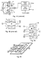
- Fig. 1A illustrates a prior art current loop 10 in a switching power supply, where the entire circuit forming the loop (e.g., transistors, wires/traces, capacitors, parasitics, etc.) adds to the magnetic field, causing EMI.
- the switches 12 and 14 are shown as MOSFETs, but may be any other type of switch, such as bipolar transistors.
- the switches 12 and 14 are shown as n-channel MOSFETs, but CMOS transistors may be used, depending on the application.
- the switches' parasitic capacitances 16 and 18 are shown.
- the switches 12 and 14 are synchronously switched to alternately couple a power supply voltage (Vcc) at terminal 1 to the output terminal 2 and then couple a ground voltage at terminal 3 to the output terminal 2.
- An inductor (not shown) may be coupled to terminal 2 as part of an output circuit 17 in a buck regulator.
- a PWM controller IC 19 is connected to the gates of the two switches 12 and 14 for controlling the switch duty cycle to output a regulated voltage Vout or regulated current.
- the duty cycle is controlled to cause a feedback voltage Vfb, proportional to the output voltage of the regulator, to match a reference voltage.
- One of the switches is referred to as the power switch and the other is the synchronous rectifier, which essentially acts as a low voltage drop diode.
- the switches 12and 14 are not both on at the same time to avoid a short circuit.
- the regulator may be any type (e.g., buck, boost, flyback, etc), and the particular connection of the switches 12 and 14 to the inductor is determined by the type of regulator.
- the present invention may be employed in any type of switching regulator, and certain examples are given to illustrate the concepts of the invention as applied to a standard buck regulator switching configuration.
- a conventional bypass capacitor 20 is shown in Fig. 1A connected between terminal 1 and terminal 3.
- Bypass capacitors are typically used in prior art switching circuits. If we assume terminal 1 is connected to Vcc and terminal 3 is ground, the bypass capacitor 20 smooths transients when the switches 12 and 14 open and close. For example, when the regulator controller closes the switch 12 to charge the inductor, there is a surge of current by the charged capacitor 20 being connected to the inductor via terminal 2. This helps offset any droop in the Vcc caused by the surge of current and smooths the switching transient.
- the capacitor 20 forms part of the current loop around terminals 2, 3, and 1.
- the parasitic capacitances 16 and 18 of the switches 12 and 14 are also part of the current loop, and the parasitic capacitor 18 charges when the switch 14 is turned off and the switch 12 is turned on.
- the switches 12 and 14 may be within an IC 21 and may be part of the PWM controller IC 19.
- Fig. 1B is another representation of the circuit of Fig. 1A , which illustrates the transistor switch locations on a printed circuit board (PCB) or in an IC package.
- the terminals 1, 2, and 3 may be the connection nodes for the pins extending from the IC package.
- the current loop 10 shows the transient current flowing in a counter-clockwise direction, causing the direction of the magnetic field to be upwards, represented by a dot. The magnetic field emanates in all directions in a certain pattern.
- US 2011/0128074 A1 relates to a primitive cell including an internal circuit, a power supply wire that applies a power supply voltage to the internal circuit, and a ground wire that applies a ground voltage to the internal circuit, in which the power supply wire and the ground wire are arranged so as to be localized in one side of out peripheral sides of the cell.
- US 2010/0038735 A1 relates to a transistor device which includes a magnetic field source adapted to deflect a flow of free electron carriers within a channel of the device, between a source region and a drain region thereof.
- the magnetic field source includes a magnetic material layer extending over a side of the channel that is opposite a date electrode of the transistor device.
- What is needed is a technique for reducing the overall magnetic field generated by a switching regulator in order to reduce EMI.
- aspects of the invention seek to provide a switching regulator that generates a greatly reduced overall magnetic field, where the magnetic field is associated with quickly changing switch currents.
- Techniques according to embodiments of the invention split the prior art single magnetic loop into multiple magnetic loops (each incorporating a high frequency switch), where the multiple loops have linked opposing magnetic fields that cancel each other out, resulting in a much lower overall magnetic field and EMI compared to prior art designs.
- Planar construction includes integrated circuits and printed circuit boards.
- 3-D construction includes stacked (vertically oriented) loop components, stacked integrated circuit elements, and stacked printed circuit boards.
- a topside power switch and synchronous rectifier switch are divided and arranged as follows.
- the bottomside switch is divided into two identical bottomside switches operated in parallel, and the bottomside switches are arranged on opposite sides of the topside switch, in a planar embodiment.
- a first bypass capacitor is connected between the first bottomside switch and the topside switch, and a second bypass capacitor is connected between the second bottomside switch and the topside switch.
- the configurations are essentially mirror images, with the topside switch in the middle. If we assume the topside switch has just been turned on, the current loop through the topside switch and the first bottomside switch is counter-clockwise, and the current loop through the topside switch and the second bottomside switch is clockwise. The directions of the two magnetic fields created are opposite. Since the loops are very close, the generated magnetic fields substantially cancel out, so the overall magnetic field emanating from the regulator is greatly reduced, reducing EMI.
- the technique may be applied to also dividing up the topside switch, where a first pair of topside and bottomside switches creates a first current loop in one direction, and a second pair of topside and bottomside switches creates a second current loop in the opposite direction to produce cancelling magnetic fields.
- topside switch and bottom side switch are divided up into four bottomside switches and two topside switches that form four current loops that oppose each other in the x and y directions to create an even lower overall magnetic field.
- bypass capacitor may be located overlying the switches.
- switches may be stacked or the PCBs may be stacked to cancel out the magnetic fields produced by each level.
- a single current path is formed in a figure 8 shape to create two opposing current loops, resulting in the cancellation of the magnetic fields.
- the gates of the MOSFET switches are assumed to be connected to a conventional synchronous PWM controller for a DC-DC converter, and a conventional output circuit is connected to the terminals 1, 2, and 3, as needed for the particular type of converter.
- the output circuit typically comprises one or more inductors and one or more large smoothing capacitors.
- the datasheet for the LT8611 Synchronous Step-Down Regulator available on-line from the Linear Technology Corporation website, illustrates a suitable PWM controller for the switches described herein, as well as an output circuit, and is incorporated herein by reference as a typical example of a PWM controller and output circuit for synchronous switches.
- Other suitable PWM controllers and output circuits are described in US Patents 5,731,731 and 5,847,554 , assigned to the present assignee and incorporated herein by reference.
- the controllers may switch at a fixed frequency or a variable frequency.
- magnetic loop cancellation in planar structures is accomplished by dividing the switches into multiple switch portions and electrically interconnecting them to create a plurality of similar current loops but having opposite directions. This configuration places opposing magnetic fields in close proximity to achieve an overall lower magnetic field emanation.
- one or more components such as the wires/traces or the bypass capacitor
- the current loops are above the IC or PCB surface to create opposite vertical current loops to achieve an overall lower magnetic field.
- Fig. 2A illustrates how the switching circuit of Fig. 1A can be broken up into multiple loops that conduct current in opposite directions, causing the magnetic fields to have opposite directions (shown by the dot and x) to partially cancel out the magnetic fields created by each loop. Therefore, the overall magnetic field emitted by the circuit is reduced. Magnetic field cancellations of 50% and higher can be obtained for a planar construction.
- the bottom switch 14 in Fig. 1A is replaced by two switches 14A and 14B in parallel, and the two switches sandwich the other switch 12 (the high side switch) in the plane.
- the opposing current loops 24 and 25 are placed as close together as practical on the chip or PCB to improve the cancellation.
- the bypass capacitor 20 in Fig. 1A is replaced by bypass capacitors 20A and 20B to perform the same function as the bypass capacitor 20.
- the switches 14A and 14B may each be half the size of the switch 14, so there is not a large increase in size.
- the switches 14A and 14B may be MOSFETs, bipolar transistors, or any other switching elements controlled by the switching regulator controller IC 19, and the switches may be on the PWM controller IC 19.
- the terminal 2 may be connected to the output circuit 17 of Fig. 1A .
- Fig. 2A illustrates a planar circuit construction. Magnetic field cancellation may also be achieved by creating a 3-D structure, described later.
- Fig. 2B illustrates the layout of the switches of Fig. 2A on an IC 28, which may also contain the control circuitry.
- All bypass capacitors in all embodiments may be located internal to the package or external to the package. Providing the capacitors internal to the package better ensures the symmetrical relationships of the opposite magnetic fields for optimal cancellation.
- synchronously switch transistors are used in the example, other types of switching regulators may turn off both switches concurrently, such as in a sleep mode of operation or a discontinuous mode.
- the synchronous rectifier switch may be controlled by a reverse voltage detection circuit rather than being synchronously switched with the other switch.
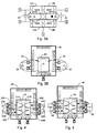
- Fig. 3A illustrates another example of how the switching circuit of Fig. 1A can be broken up to create multiple current loops 30/32 that conduct current in opposite directions, causing the magnetic fields to have opposite directions or polarities (shown by the dot and x) to partially cancel out the magnetic fields created by each loop.
- the bypass capacitors 34 and 36 are also shown as part of each loop.
- the bottom switch 14 in Fig. 1A is replaced by two switches 14A and 14B connected in parallel
- the top switch 12 in Fig. 1A is replaced by two switches 12A and 12B connected in parallel.
- the circuit is laid out on the PCB or in silicon so the opposite direction loops are placed as close together as practical to improve the cancellation.
- Each switch e.g., a MOSFET
- Fig. 3B is a semi-transparent top down view of a package 38 for one or more ICs, showing the package pin layout and the pins corresponding to the terminals 1, 2, and 3 in Fig. 3A .
- the terminals 1,2, and 3 may be connection nodes on a PCB.
- the package has 20 peripheral pins and a center ground pad 21 for connection to a ground pin or a pad on the PCB.
- the outline of an IC 42 is shown, which contains the two sets of switches in Fig. 3A .
- the terminals on the IC 42 may be connected to the pins of the package 38 by bond wires, a lead frame, a PCB, or other connectors. Multiple terminals and pins may be connected together to handle higher currents and/or to create a desirable current loop pattern.
- the magnetic field cancellation in Fig. 2B and 3B is different in the x and y directions, due to the asymmetry of the structure.
- the configuration of Fig. 4 may be used.
- Fig. 4 an outline of an IC 44 is shown along with exposed pads 21A and 21B.
- the IC 44 contains six switches, where a mirror image of the switch configuration in Fig. 2B is created by dividing the switches 14A, 14B, and 12 to create the equal but opposite current loops 24A and 25B, and 24B and 25B. Additional bypass capacitors 24B and 25B are connected to the terminals 1 and 3. The resulting magnetic fields symmetrically cancel each other out to lower EMI in all directions.
- the terminals 1, 2, and 3 e.g., nodes on a PCB for connection to the power supply and bypass capacitors
- the terminals 1, 2, and 3 should be close to the associated package pins (pins 4-13) to create four similar current loop structures. The selection of the package pins (forming part of the current loops) is thus important to create current loops with similar shapes that are very close together.
- Pins may be tied together to reduce resistance and to help cancel the magnetic fields.
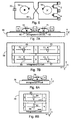
- Fig. 5 illustrates another circuit arrangement, using the same package 46 and IC 44 in Fig. 4 , where only two bypass capacitors 48 and 50 are used.
- the opposing current loops 24A and 25B, and 24B and 25B, can each share a bypass capacitor 48 or 50.
- Each bypass capacitor in Fig. 5 (48 or 50) is optimally placed symmetrically between its associated outer switches (e.g., switches 14A and 14B in Fig. 2B ) so as to be substantially equidistant from each associated outer switch to equalize the opposite magnetic fields.
- the switches do not have to be formed on the same silicon chip, and multiple silicon chips may be interconnected within a single package, where the interconnections (e.g., wires or traces) are part of the current loop.
- the goal of the various switch/capacitor arrangements is to provide a minimum of two current paths generating similar but opposite magnetic field properties. This may be accomplished in ways other than those described with respect to Figs. 2A-5 . Figs. 6-8B illustrate a few of those other ways.
- Fig. 6 illustrates a cross-wiring configuration for the switches 12 and 14, connected to the bypass capacitor 20, that creates opposing current loops 52 and 54 in the IC or PCB for reducing the overall magnetic field generated.
- the cancellation current loop forms a figure 8 shape, which includes rounded figure 8 shapes as well as rectilinear figure 8 shapes.
- the two or more opposite current loops are made by crossing the wires 55 or traces with an insulating layer in-between.
- the wires/traces 55 may be internal or external to the IC or partially internal and external.
- the bypass capacitor 20 can be at any position in the current loop, such as at the crossing point.
- the crossing point can then be placed under the capacitor.
- Figs. 7A and 7B illustrate a side view and top down view, respectively, of a circuit configuration in an IC 58 where the opposing current loops 60 and 62 have a vertical component for cancelling out the magnetic fields 64, 65, 66, and 67 in Fig. 7B .
- the directions of the magnetic fields are shown by arrows.
- the magnetic field cancellation is formed by attaching bypass capacitors 70, 71, 72, and 72 over the IC 58 to create vertical current loops, rather than planar loops.
- the six switches comprise the topside switch divided into three parallel switches and the bottomside switch divided into three parallel switches in the arrangement indicated in Fig. 7B . Note how the top half of Fig.
- FIG. 7B has two bottomside switches (coupled to the terminals 3 and 2) sandwiching the central topside switch (coupled to terminals 1 and 2), and the bottom half of Fig. 7B has two topside switches (coupled to the terminals 1 and 2) sandwiching the central bottomside switch (coupled to terminals 3 and 2) to form an asymmetrical arrangement.
- Figs. 8A and 8B illustrates a side view and top down view of another embodiment of vertical circuits in an IC 76 with opposite-direction current loops 78 (only one current loop is shown in Fig. 8A ) for cancelling out the magnetic fields 80 and 82 in Fig. 8B .
- Fig. 8B there are four switches, where the topside switch is divided into two parallel switches, and the bottomside switch is divided into two parallel switches in the arrangement indicated in Fig. 8B.
- Fig. 8B is essential the left half of the circuit of Fig. 7B , where, in Fig. 8B , each switch is larger to carry half the current.
- magnetic loop cancellation in a 3-D construction is formed by forming multiple power switch devices with paths for circulating current in a vertically oriented mirror image configuration.
- the structure is designed to crate opposing loops of current to generate antiparallel magnetic fields for a cancellation effect.
- the overall magnetic field induced due to net currents flowing through two or more cancelling current loops is less than the sum of the absolute magnetic fields of the individual loops or a comparable loop of a prior art single loop design in any plane cutting through the 2 or 3 dimensional cancellation design. Accordingly, there is less EMI by using the techniques of the present invention.
- the invention still operates to lower EMI to a lesser degree even when the opposing magnetic fields have different magnitudes, such as where the current loops have different loop radii or shapes.
Description
- This invention relates to switching regulators and, in particular, to a technique to reduce electromagnetic interference (EMI) caused by the magnetic fields created by high frequency switching.
- Switching regulators typically switch at frequencies from 100KHz-SMHz. Small current loops that are created at such high speeds can generate significant magnetic fields. If the switches are formed in an integrated circuit (IC), the current loops may occur entirely within the IC or partially internal and partially external to the IC. If a loop conducts an initial transient current due to the power switch closing or a synchronous rectifier switch closing, the relatively high di/dt results in a high magnetic field that may create electromagnetic interference (EMI).
-
Fig. 1A illustrates a prior artcurrent loop 10 in a switching power supply, where the entire circuit forming the loop (e.g., transistors, wires/traces, capacitors, parasitics, etc.) adds to the magnetic field, causing EMI. Theswitches switches parasitic capacitances - In the example, it is assumed that the
switches terminal 1 to theoutput terminal 2 and then couple a ground voltage atterminal 3 to theoutput terminal 2. An inductor (not shown) may be coupled toterminal 2 as part of anoutput circuit 17 in a buck regulator. In one example of a regulator, aPWM controller IC 19 is connected to the gates of the twoswitches - The regulator may be any type (e.g., buck, boost, flyback, etc), and the particular connection of the
switches - A
conventional bypass capacitor 20 is shown inFig. 1A connected betweenterminal 1 andterminal 3. Bypass capacitors are typically used in prior art switching circuits. If we assumeterminal 1 is connected to Vcc andterminal 3 is ground, thebypass capacitor 20 smooths transients when theswitches switch 12 to charge the inductor, there is a surge of current by thecharged capacitor 20 being connected to the inductor viaterminal 2. This helps offset any droop in the Vcc caused by the surge of current and smooths the switching transient. Thecapacitor 20 forms part of the current loop aroundterminals parasitic capacitances switches parasitic capacitor 18 charges when theswitch 14 is turned off and theswitch 12 is turned on. - As seen, there is a very fast and high current pulse (having a large di/dt) being generated through the
loop 10 at the switching frequency. This pulse generates EMI, which may interfere with or create distortion in nearby electrical circuits. - The
switches IC 21 and may be part of the PWM controller IC 19. -
Fig. 1B is another representation of the circuit ofFig. 1A , which illustrates the transistor switch locations on a printed circuit board (PCB) or in an IC package. Theterminals current loop 10 shows the transient current flowing in a counter-clockwise
direction, causing the direction of the magnetic field to be upwards, represented by a dot. The magnetic field emanates in all directions in a certain pattern. -
US 2011/0128074 A1 relates to a primitive cell including an internal circuit, a power supply wire that applies a power supply voltage to the internal circuit, and a ground wire that applies a ground voltage to the internal circuit, in which the power supply wire and the ground wire are arranged so as to be localized in one side of out peripheral sides of the cell. -
US 2010/0038735 A1 relates to a transistor device which includes a magnetic field source adapted to deflect a flow of free electron carriers within a channel of the device, between a source region and a drain region thereof. According to preferred configurations, the magnetic field source includes a magnetic material layer extending over a side of the channel that is opposite a date electrode of the transistor device. - What is needed is a technique for reducing the overall magnetic field generated by a switching regulator in order to reduce EMI.
- Aspects of the invention seek to provide a switching regulator that generates a greatly reduced overall magnetic field, where the magnetic field is associated with quickly changing switch currents.
- Techniques according to embodiments of the invention split the prior art single magnetic loop into multiple magnetic loops (each incorporating a high frequency switch), where the multiple loops have linked opposing magnetic fields that cancel each other out, resulting in a much lower overall magnetic field and EMI compared to prior art designs.
- The magnetic field cancellation techniques of the invention are applicable to both planar and 3-dimensional (3-D) switching circuits in switch mode power supplies. Planar construction includes integrated circuits and printed circuit boards. 3-D construction includes stacked (vertically oriented) loop components, stacked integrated circuit elements, and stacked printed circuit boards.
- In one embodiment, a topside power switch and synchronous rectifier switch (the bottomside switch) are divided and arranged as follows. The bottomside switch is divided into two identical bottomside switches operated in parallel, and the bottomside switches are arranged on opposite sides of the topside switch, in a planar embodiment. A first bypass capacitor is connected between the first bottomside switch and the topside switch, and a second bypass capacitor is connected between the second bottomside switch and the topside switch. The configurations are essentially mirror images, with the topside switch in the middle. If we assume the topside switch has just been turned on, the current loop through the topside switch and the first bottomside switch is counter-clockwise, and the current loop through the topside switch and the second bottomside switch is clockwise. The directions of the two magnetic fields created are opposite. Since the loops are very close, the generated magnetic fields substantially cancel out, so the overall magnetic field emanating from the regulator is greatly reduced, reducing EMI.
- The technique may be applied to also dividing up the topside switch, where a first pair of topside and bottomside switches creates a first current loop in one direction, and a second pair of topside and bottomside switches creates a second current loop in the opposite direction to produce cancelling magnetic fields.
- In another embodiment, the topside switch and bottom side switch are divided up into four bottomside switches and two topside switches that form four current loops that oppose each other in the x and y directions to create an even lower overall magnetic field.
- Similar techniques may be used for 3-D configurations where the opposing current loops are vertically oriented. For example, the bypass capacitor may be located overlying the switches.
- Further, the switches may be stacked or the PCBs may be stacked to cancel out the magnetic fields produced by each level.
- In another embodiment a single current path is formed in a
figure 8 shape to create two opposing current loops, resulting in the cancellation of the magnetic fields. - Other embodiments are envisioned.
-
-
Fig. 1A illustrates a prior art switching circuit used in conventional switching regulators. -
Fig. 1B is a different representation ofFig. 1A , showing locations of the transistor switches on an IC or PCB. -
Fig. 2A illustrates a switching configuration that accomplishes the switching function of the circuit ofFig. 1A but with much less EMI. -
Fig. 2B is a perspective view of a portion of an IC or PCB presenting a different representation ofFig. 2A , showing locations of the transistor switches on the IC or PCB. -
Fig. 3A illustrates another configuration of switches that further reduces EMI yet accomplishes the switching function of the circuit ofFig. 1A . -
Fig. 3B is a semi-transparent top down view of a package for one or more ICs, showing the package pin layout and the pins corresponding to the terminals inFig. 3A . -
Fig. 4 is a semi-transparent top down view of a package for an IC, showing the package pin layout and the pins corresponding to the terminals in a switch configuration, where the three switches ofFig. 2B have been divided into a total of six switches and positioned as mirror images in the package to further reduce EMI. -
Fig. 5 has the same switch arrangement asFig. 4 but a different bypass capacitor connection, saving two capacitors while maintaining reduced EMI. -
Fig. 6 illustrates how cross-over wiring in afigure 8 shape may create opposite current loops. -
Fig. 7A is a side view of an IC containing six switches, such as the switches ofFig. 4 , where the bypass capacitors are stacked above the transistors to form opposite vertical current loops to reduce EMI. -
Fig. 7B is a top down view of the IC ofFig. 7A , whereFig. 7A is a side view from the upper side ofFig. 7B . -
Fig. 8A is a side view of an IC containing four switches, where the bypass capacitors are stacked above the transistors to form opposite vertical current loops to reduce EMI. -
Fig. 8B is a top down view of the IC ofFig. 8A , whereFig. 8A is a side view from the upper side ofFig. 8B . - In the figures, elements that are the same or equivalent are labeled with the same numeral.
- In all embodiments, the gates of the MOSFET switches are assumed to be connected to a conventional synchronous PWM controller for a DC-DC converter, and a conventional output circuit is connected to the
terminals US Patents 5,731,731 and5,847,554 , assigned to the present assignee and incorporated herein by reference. The controllers may switch at a fixed frequency or a variable frequency. - In accordance with the present invention, magnetic loop cancellation in planar structures is accomplished by dividing the switches into multiple switch portions and electrically interconnecting them to create a plurality of similar current loops but having opposite directions. This configuration places opposing magnetic fields in close proximity to achieve an overall lower magnetic field emanation. In a vertical structure, one or more components (such as the wires/traces or the bypass capacitor) in the current loops are above the IC or PCB surface to create opposite vertical current loops to achieve an overall lower magnetic field.
-
Fig. 2A illustrates how the switching circuit ofFig. 1A can be broken up into multiple loops that conduct current in opposite directions, causing the magnetic fields to have opposite directions (shown by the dot and x) to partially cancel out the magnetic fields created by each loop. Therefore, the overall magnetic field emitted by the circuit is reduced. Magnetic field cancellations of 50% and higher can be obtained for a planar construction. - In
Fig. 2A , thebottom switch 14 inFig. 1A is replaced by twoswitches current loops bypass capacitor 20 inFig. 1A is replaced bybypass capacitors bypass capacitor 20. Theswitches switch 14, so there is not a large increase in size. Theswitches regulator controller IC 19, and the switches may be on thePWM controller IC 19. Theterminal 2 may be connected to theoutput circuit 17 ofFig. 1A . -
Fig. 2A illustrates a planar circuit construction. Magnetic field cancellation may also be achieved by creating a 3-D structure, described later. -
Fig. 2B illustrates the layout of the switches ofFig. 2A on anIC 28, which may also contain the control circuitry. - All bypass capacitors in all embodiments may be located internal to the package or external to the package. Providing the capacitors internal to the package better ensures the symmetrical relationships of the opposite magnetic fields for optimal cancellation.
- Although, synchronously switch transistors are used in the example, other types of switching regulators may turn off both switches concurrently, such as in a sleep mode of operation or a discontinuous mode. The synchronous rectifier switch may be controlled by a reverse voltage detection circuit rather than being synchronously switched with the other switch.
-
Fig. 3A illustrates another example of how the switching circuit ofFig. 1A can be broken up to create multiplecurrent loops 30/32 that conduct current in opposite directions, causing the magnetic fields to have opposite directions or polarities (shown by the dot and x) to partially cancel out the magnetic fields created by each loop. Thebypass capacitors Fig. 3A , thebottom switch 14 inFig. 1A is replaced by twoswitches top switch 12 inFig. 1A is replaced by twoswitches -
Fig. 3B is a semi-transparent top down view of apackage 38 for one or more ICs, showing the package pin layout and the pins corresponding to theterminals Fig. 3A . Theterminals center ground pad 21 for connection to a ground pin or a pad on the PCB. The outline of anIC 42 is shown, which contains the two sets of switches inFig. 3A . The terminals on theIC 42 may be connected to the pins of thepackage 38 by bond wires, a lead frame, a PCB, or other connectors. Multiple terminals and pins may be connected together to handle higher currents and/or to create a desirable current loop pattern. - The magnetic field cancellation in
Fig. 2B and3B is different in the x and y directions, due to the asymmetry of the structure. To create a more symmetrical cancellation structure, the configuration ofFig. 4 may be used. - In
Fig. 4 , an outline of anIC 44 is shown along with exposedpads IC 44 contains six switches, where a mirror image of the switch configuration inFig. 2B is created by dividing theswitches current loops Additional bypass capacitors terminals terminals - Pins may be tied together to reduce resistance and to help cancel the magnetic fields.
-
Fig. 5 illustrates another circuit arrangement, using thesame package 46 andIC 44 inFig. 4 , where only twobypass capacitors current loops bypass capacitor - Each bypass capacitor in
Fig. 5 (48 or 50) is optimally placed symmetrically between its associated outer switches (e.g., switches 14A and 14B inFig. 2B ) so as to be substantially equidistant from each associated outer switch to equalize the opposite magnetic fields. - The combination of the switch configuration, the bypass capacitor configuration, the wiring from the package to the IC leads, any internal traces in the package, the metal conductor configuration in the IC, the IC/package terminal/pin arrangement, and the PCB traces all must be considered to achieve the maximum amount of magnetic field cancelling.
- In all embodiments, the switches do not have to be formed on the same silicon chip, and multiple silicon chips may be interconnected within a single package, where the interconnections (e.g., wires or traces) are part of the current loop.
- The goal of the various switch/capacitor arrangements is to provide a minimum of two current paths generating similar but opposite magnetic field properties. This may be accomplished in ways other than those described with respect to
Figs. 2A-5 .Figs. 6-8B illustrate a few of those other ways. -
Fig. 6 illustrates a cross-wiring configuration for theswitches bypass capacitor 20, that creates opposingcurrent loops figure 8 shape, which includes roundedfigure 8 shapes as well as rectilinearfigure 8 shapes. The two or more opposite current loops are made by crossing thewires 55 or traces with an insulating layer in-between. The wires/traces 55 may be internal or external to the IC or partially internal and external. - The
bypass capacitor 20 can be at any position in the current loop, such as at the crossing point. The crossing point can then be placed under the capacitor. -
Figs. 7A and 7B illustrate a side view and top down view, respectively, of a circuit configuration in anIC 58 where the opposingcurrent loops magnetic fields Fig. 7B . The directions of the magnetic fields are shown by arrows. The magnetic field cancellation is formed by attachingbypass capacitors IC 58 to create vertical current loops, rather than planar loops. There are four vertical current loops created using six switches which cancel the magnetic field in all directions. The six switches comprise the topside switch divided into three parallel switches and the bottomside switch divided into three parallel switches in the arrangement indicated inFig. 7B . Note how the top half ofFig. 7B has two bottomside switches (coupled to theterminals 3 and 2) sandwiching the central topside switch (coupled toterminals 1 and 2), and the bottom half ofFig. 7B has two topside switches (coupled to theterminals 1 and 2) sandwiching the central bottomside switch (coupled toterminals 3 and 2) to form an asymmetrical arrangement. -
Figs. 8A and 8B illustrates a side view and top down view of another embodiment of vertical circuits in anIC 76 with opposite-direction current loops 78 (only one current loop is shown inFig. 8A ) for cancelling out themagnetic fields Fig. 8B . InFig. 8B , there are four switches, where the topside switch is divided into two parallel switches, and the bottomside switch is divided into two parallel switches in the arrangement indicated inFig. 8B. Fig. 8B is essential the left half of the circuit ofFig. 7B , where, inFig. 8B , each switch is larger to carry half the current. - Generally, magnetic loop cancellation in a 3-D construction is formed by forming multiple power switch devices with paths for circulating current in a vertically oriented mirror image configuration. The structure is designed to crate opposing loops of current to generate antiparallel magnetic fields for a cancellation effect.
- Close proximity of the loops, such as in the same IC package, have better cancellation but even a larger distance still improves cancellation compared to prior art single loop designs.
- In the various embodiments described, the overall magnetic field induced due to net currents flowing through two or more cancelling current loops is less than the sum of the absolute magnetic fields of the individual loops or a comparable loop of a prior art single loop design in any plane cutting through the 2 or 3 dimensional cancellation design. Accordingly, there is less EMI by using the techniques of the present invention.
- Although, in the various embodiments, the magnitudes of the opposing magnetic fields have been identical, the invention still operates to lower EMI to a lesser degree even when the opposing magnetic fields have different magnitudes, such as where the current loops have different loop radii or shapes.
- The same cancellation that lowers EMI also results in lower parasitic inductances, which are a loss mechanism at high switching frequencies. Therefore, the present cancellation technique results more efficient power supplies at high switching frequencies compared to the prior art. This is an unexpected and surprising result of the magnetic field cancellation technique.
Claims (27)
- A switching regulator circuit comprising:a controller (19) for generating transistor switch control signals;a first switch (12) controlled by the controller, the controller (19) controlling the first switch (12) at a duty cycle to control the regulated output of the switching regulator circuit;a first bypass capacitor (20) coupled to the first switch (12) as part of a current loop with the first switch (12); andat least a first current loop (52) and a second current loop (54) being simultaneously created by switching of the first switch (12), wherein a first current flows in the first current loop (52) in a first direction to generate a first magnetic field having a first magnitude in a first direction, wherein a second current flows in the second current loop (54) in a second direction, opposite to the first direction, to generate a second magnetic field having a second magnitude in a second direction, such that the first magnetic field and the second magnetic field combine to reduce electromagnetic interference - EMI - generated by the switching regulator circuit;a first conductor (55) connected between a first terminal of the first switch (12) and a first terminal of the first bypass capacitor (20); anda second conductor connected between a second terminal of the bypass capacitor (20) and a reference voltage,wherein the first conductor (55) and the second conductor cross over one another to form a figure 8 shape forming the first current loop (52) and the second current loop (54) conducting currents in opposite directions.
- The circuit of Claim 1 wherein the figure 8 shape is constructed by forming the cross over point underneath the first bypass capacitor (20).
- A switching regulator circuit receiving an input voltage and generating a regulated output, the circuit comprising:a controller (19) for generating transistor switch control signals;a first switch (14A) controlled by the controller (19), the controller (19) controlling the first switch (14A) at a duty cycle to control the regulated output of the switching regulator circuit;a first bypass capacitor (20A) coupled to the first switch as part of a current loop with the first switch (14A); anda second switch (14B) connected in parallel with the first switch (14A), the second switch (14B) being controlled by the controller (19) to be in the same state as the first switch (14A) so as to have the same duty cycle as the first switch (14A) to control the regulated output of the switching regulator circuit,wherein the first switch (14A) is positioned to create a first current loop (25) when switched into its conductive state, wherein a first current flows in the first current loop (25) in a first direction to generate a first magnetic field having a first magnitude in a first direction,wherein the second switch (14B) is positioned to create a second current loop (24) when switched into its conductive state, wherein a second current flows in the second current loop (24) in a second direction, opposite to the first direction, to generate a second magnetic field having a second magnitude in a second direction, such that the first magnetic field and the second magnetic field combine to reduce electromagnetic interference - EMI - generated by the switching regulator circuit.
- The circuit of Claim 3 wherein the first magnitude is the same as the second magnitude.
- The circuit of Clam 3 or 4 further comprising:a third switch (12),wherein the first switch (14A) and the second switch (14B) are located on opposite sides of the third switch (12) such that the first current loop (25) is created by the first current flowing into the first switch (14A) and the third (12) switch, and the second current loop is created by the second current flowing into the second switch (14B) and the third switch (12).
- The circuit of Claim 5 wherein, when the first switch (14A) and second switch (14B) are on and the third switch (12) is off, the first current flows through the first switch (14A) and into a parasitic capacitor of the third switch (12), and the second current flows through the second switch (14B) and into the parasitic capacitor of the third switch (12).
- The circuit of Claim 5 or 6 wherein the first bypass capacitor (20A) is coupled between the third switch (12) and the first switch (14A), and wherein the first bypass capacitor (20A) is part of the first current loop (25).
- The circuit of Claim 7 further comprising a second bypass capacitor (20B) coupled between the third switch (12) and the second switch (14B), and wherein the second bypass capacitor (20B) is part of the second current loop (24).
- The circuit of Claim 7 wherein the first bypass capacitor (20A) is also coupled between the third switch (12) and the second switch (14B), and wherein the first bypass capacitor (20A) is also part of the second current loop (24).
- The circuit of Claim 9 wherein the first bypass capacitor (20A) is placed symmetrically between the first switch (14A) and the second switch (14B) so as to be equidistant from the first switch (14A) and the second switch (14B).
- The circuit of Claim 3 or 4 further comprising:a third switch (12A) and a fourth switch (12B) connected in parallel so as to conduct simultaneously, wherein the third switch (12A) is positioned opposing the first switch (14A), wherein the fourth switch (12B) is positioned opposing the second switch (14B), wherein the fourth switch (12B) is next to the third switch (12A), and wherein the first switch (14A) is next to the second switch (14B), such that the first current loop (30) is created by the first current flowing into the first switch (14A) and the third switch (12A), and the second current loop (32) is created by the second current flowing into the second switch (14B) and the fourth switch (12B).
- The circuit of Claim 11 wherein, when the first switch (14A) and second switch (14B) are on, and when the third switch (12A) and fourth switch (12B) are off, the first current flows through the first switch (14A) and into a parasitic capacitor of the third switch (12A), and the second current flows through the second switch (14B) and into the parasitic capacitor of the fourth switch (12B).
- The circuit of Claim 11 or 12 wherein the first bypass capacitor (34) is coupled between the third switch (12A) and the first switch (14A), and wherein the first bypass capacitor (34) is part of the first current loop (30).
- The circuit of Claim 13 further comprising a second bypass capacitor (36) coupled between the fourth switch (12B) and the second switch (14B), and wherein the second bypass capacitor (36) is part of the second current loop (32).
- The circuit of Claim 3 or 4 further comprising:a third switch (12A) and a fourth switch (12B) connected in parallel so as to be switched simultaneously and switched oppositely to the switching of the first switch (14A) and the second switch (14B);wherein the first switch (14A) and the second switch (14B) are positioned to oppose the third switch (12A) and the fourth switch (12B) to create opposing pairs of switches,wherein the opposing pairs create a plurality of current loops, including the first current loop (30) and the second current loop (32), wherein some current loops flow in a direction opposite to other ones of the current loops to create a plurality of magnetic fields having opposite directions to reduce EMI generated by the switching regulator circuit.
- The circuit of Claim 15 further comprising a plurality of bypass capacitors (34, 36), including the first bypass capacitor (34), wherein associated ones of the bypass capacitors are coupled between the first switch (14A), the second switch (14B), the third switch (12A), and the fourth switch (12B) to form the current loops (30, 32).
- The circuit of Claim 16 wherein at least four current loops (24A, 24B, 25A, 25C) are created comprising the first current loop (24A) and the second current loop (24B), and a third current loop (25A) and a fourth current loop (25B), wherein a direction of current in the third current loop (25A) is opposite a direction of current in the fourth current loop (25B).
- The circuit of any preceding Claim wherein the first current loop (52, 24) and the second current loop (54, 25) are planar, parallel to a surface of a substrate on which the first switch (14A) andr the second switch (14B) are formed.
- The circuit of any of Claims 3 to 17 wherein the first current loop (60) and the second current loop (62) have vertical components that are non-planar with respect to a surface of a substrate on which the first switch (14A) and the second switch (14B) are formed.
- The circuit of Claim 19 wherein the first bypass capacitor (70) is non-planar with the first switch (14A) and the second switch (14B).
- The circuit of any preceding Claim wherein the first switch (14A) and the second switch (14B) are MOSFETs.
- The circuit of any preceding Claim wherein the first switch (14A) and the second switch (14B) are formed on an integrated circuit chip (46, 48).
- The circuit of Claim 22 wherein the integrated circuit chip (46) has alternating or interleaved external terminals to the first switch (14A) and the second switch (14B).
- The circuit of Claim 22 wherein the integrated circuit chip (46) has two sets of external terminals to the first switch (14A) and the second switch (14B), one set on each side of the integrated circuit package.
- The circuit of any of Claims 22 to 24 wherein the integrated circuit chip (46) utilizes a plurality of capacitors (20, 48, 50) external to an integrated circuit package housing the chip to connect to all or a subset of the terminals of the first switch (14A) and the second switch (14B).
- The circuit of any of Claims 22 to 24 wherein the integrated circuit chip (46) utilizes a plurality of capacitors internal to an integrated circuit package housing the chip to connect to the first switch (14A) and the second switch (14B) in several locations.
- The circuit of any preceding Claim wherein the first switch (14A) and the second switch (14B) are housed in a same package having terminals, where the terminals are arranged on the package such that, when the first bypass capacitor (48) is connected to the terminals external the package, the first current loop (25) and the second current loop (24) are formed.
Applications Claiming Priority (2)
| Application Number | Priority Date | Filing Date | Title |
|---|---|---|---|
| US201261715947P | 2012-10-19 | 2012-10-19 | |
| US13/710,127 US8823345B2 (en) | 2012-10-19 | 2012-12-10 | Magnetic field cancellation in switching regulators |
Publications (2)
| Publication Number | Publication Date |
|---|---|
| EP2722987A1 EP2722987A1 (en) | 2014-04-23 |
| EP2722987B1 true EP2722987B1 (en) | 2016-11-16 |
Family
ID=49301324
Family Applications (1)
| Application Number | Title | Priority Date | Filing Date |
|---|---|---|---|
| EP13186691.5A Active EP2722987B1 (en) | 2012-10-19 | 2013-09-30 | Magnetic field cancellation in switching regulators |
Country Status (5)
| Country | Link |
|---|---|
| US (1) | US8823345B2 (en) |
| EP (1) | EP2722987B1 (en) |
| JP (1) | JP5779213B2 (en) |
| CN (1) | CN103780077B (en) |
| TW (1) | TWI492507B (en) |
Families Citing this family (17)
| Publication number | Priority date | Publication date | Assignee | Title |
|---|---|---|---|---|
| CN103975427B (en) | 2011-10-07 | 2017-03-01 | 沃尔泰拉半导体公司 | The power management application of interconnection substrate |
| JP6106127B2 (en) * | 2014-05-29 | 2017-03-29 | 株式会社ソニー・インタラクティブエンタテインメント | Switching converter and electronic device using the same |
| FR3035556B1 (en) | 2015-04-24 | 2017-04-21 | Continental Automotive France | METHOD FOR SYNCHRONIZING CONTROLLED CONTROL CIRCUITS CONTROLLED BY PWM CONTROL SIGNALS |
| US10110126B2 (en) | 2015-09-04 | 2018-10-23 | Dailog Semiconductor (UK) Limited | Electromagnetic interference (EMI) for pulse frequency modulation (PFM) mode of a switching regulator |
| EP3361836B1 (en) * | 2017-02-08 | 2020-06-17 | Siemens Aktiengesellschaft | Low inductance half-bridge configuration |
| JP6936022B2 (en) | 2017-03-07 | 2021-09-15 | ローム株式会社 | Printed wiring board and switching power supply using this |
| JP6440772B2 (en) * | 2017-05-26 | 2018-12-19 | 三菱電機株式会社 | Power converter |
| DE102018217763A1 (en) * | 2018-10-17 | 2020-04-23 | Mahle International Gmbh | Inverter device with half-bridge module |
| US11037883B2 (en) | 2018-11-16 | 2021-06-15 | Analog Devices International Unlimited Company | Regulator circuit package techniques |
| CN112260560B (en) * | 2019-07-05 | 2023-12-19 | 松下知识产权经营株式会社 | power conversion device |
| JP7219688B2 (en) | 2019-09-26 | 2023-02-08 | 株式会社日立製作所 | Power conversion device and its control method |
| EP3876409A1 (en) * | 2020-03-05 | 2021-09-08 | ABB Schweiz AG | Flying capacitor switching cell-system |
| CN111934539A (en) * | 2020-10-09 | 2020-11-13 | 成都正扬博创电子技术有限公司 | Anti-electromagnetic interference non-isolation DC-DC circuit board |
| CN112510988A (en) * | 2020-11-06 | 2021-03-16 | 苏州浪潮智能科技有限公司 | Anti-electromagnetic interference power circuit and operation method thereof |
| CN112467982A (en) * | 2020-11-06 | 2021-03-09 | 广州小鹏汽车科技有限公司 | Power supply circuit, circuit board and switching power supply |
| CN112803935A (en) * | 2020-12-29 | 2021-05-14 | 联合汽车电子有限公司 | High-frequency current circuit |
| CN113007883B (en) * | 2021-03-02 | 2022-04-19 | 珠海拓芯科技有限公司 | Anti-interference device, electronic equipment and air conditioner |
Family Cites Families (10)
| Publication number | Priority date | Publication date | Assignee | Title |
|---|---|---|---|---|
| JPH09140126A (en) | 1995-05-30 | 1997-05-27 | Linear Technol Corp | Method for operating adaptive switch circuit, adaptive output circuit, control circuit and switching voltage regulator |
| US5847554A (en) | 1997-06-13 | 1998-12-08 | Linear Technology Corporation | Synchronous switching regulator which employs switch voltage-drop for current sensing |
| TW200832875A (en) * | 2007-01-19 | 2008-08-01 | Murata Manufacturing Co | DC-DC converter module |
| US8461623B2 (en) * | 2008-07-10 | 2013-06-11 | Mitsubishi Electric Corporation | Power semiconductor module |
| US7948045B2 (en) | 2008-08-18 | 2011-05-24 | Seagate Technology Llc | Magnet-assisted transistor devices |
| JP2010268536A (en) * | 2009-05-12 | 2010-11-25 | Yokogawa Electric Corp | Power supply and semiconductor testing device using the same |
| JP4963505B2 (en) * | 2009-08-03 | 2012-06-27 | トヨタ自動車株式会社 | Voltage converter and electric load driving device |
| JP2011114198A (en) | 2009-11-27 | 2011-06-09 | Renesas Electronics Corp | Primitive cell and semiconductor device |
| JP2012059896A (en) * | 2010-09-08 | 2012-03-22 | Auto Network Gijutsu Kenkyusho:Kk | Circuit board and dc-dc conversion circuit |
| US9059642B2 (en) * | 2012-08-22 | 2015-06-16 | Atmel Corporation | Digitally controlled spur management technique for integrated DC-DC converters |
-
2012
- 2012-12-10 US US13/710,127 patent/US8823345B2/en active Active
-
2013
- 2013-09-30 EP EP13186691.5A patent/EP2722987B1/en active Active
- 2013-09-30 JP JP2013204019A patent/JP5779213B2/en active Active
- 2013-10-02 TW TW102135709A patent/TWI492507B/en active
- 2013-10-18 CN CN201310489165.5A patent/CN103780077B/en active Active
Non-Patent Citations (1)
| Title |
|---|
| None * |
Also Published As
| Publication number | Publication date |
|---|---|
| CN103780077B (en) | 2017-04-12 |
| CN103780077A (en) | 2014-05-07 |
| TWI492507B (en) | 2015-07-11 |
| US8823345B2 (en) | 2014-09-02 |
| JP2014087252A (en) | 2014-05-12 |
| TW201419732A (en) | 2014-05-16 |
| US20140111174A1 (en) | 2014-04-24 |
| EP2722987A1 (en) | 2014-04-23 |
| JP5779213B2 (en) | 2015-09-16 |
Similar Documents
| Publication | Publication Date | Title |
|---|---|---|
| EP2722987B1 (en) | Magnetic field cancellation in switching regulators | |
| US10027228B2 (en) | Switching converter having noise cancellation feature and electronic device using the same | |
| US10033275B2 (en) | DC-DC converter with a switching transistor arranged in an area where an inductor overlaps a substrate | |
| US7268659B2 (en) | Micro electric power converter | |
| US20130127434A1 (en) | Coupled Inductor Arrays And Associated Methods | |
| US8085553B1 (en) | Lead assembly for a flip-chip power switch | |
| US10620654B2 (en) | Alternatingly-switched parallel circuit, integrated power module and integrated power package | |
| US8748960B2 (en) | Multi-layer integrated circuit package | |
| US10985645B2 (en) | Alternatingly-switched parallel circuit, integrated power module and integrated power package | |
| JP6103122B1 (en) | Signal relay board for power semiconductor modules | |
| US10980109B2 (en) | Printed circuit board and switching power supply | |
| US10103627B2 (en) | Packaged integrated circuit including a switch-mode regulator and method of forming the same | |
| US9767947B1 (en) | Coupled inductors enabling increased switching stage pitch | |
| KR20140077104A (en) | Power supply device | |
| CN113950727A (en) | Stacked matrix transformer | |
| US9054088B2 (en) | Multi-component chip packaging structure | |
| JP2013004683A (en) | Power converter of printed board | |
| KR20220057400A (en) | Multi-layer Circuit assembly for reducing parasitic inductance | |
| JP2019091804A (en) | Power semiconductor module and electronic equipment |
Legal Events
| Date | Code | Title | Description |
|---|---|---|---|
| PUAI | Public reference made under article 153(3) epc to a published international application that has entered the european phase |
Free format text: ORIGINAL CODE: 0009012 |
|
| AK | Designated contracting states |
Kind code of ref document: A1 Designated state(s): AL AT BE BG CH CY CZ DE DK EE ES FI FR GB GR HR HU IE IS IT LI LT LU LV MC MK MT NL NO PL PT RO RS SE SI SK SM TR |
|
| AX | Request for extension of the european patent |
Extension state: BA ME |
|
| 17P | Request for examination filed |
Effective date: 20140918 |
|
| RBV | Designated contracting states (corrected) |
Designated state(s): AL AT BE BG CH CY CZ DE DK EE ES FI FR GB GR HR HU IE IS IT LI LT LU LV MC MK MT NL NO PL PT RO RS SE SI SK SM TR |
|
| RIN1 | Information on inventor provided before grant (corrected) |
Inventor name: KUECK, CHRISTIAN Inventor name: WITT, JEFFREY Inventor name: CHENG, DANIEL Inventor name: GARDNER, JOHN Inventor name: SHTARGOT, LEONARD |
|
| GRAP | Despatch of communication of intention to grant a patent |
Free format text: ORIGINAL CODE: EPIDOSNIGR1 |
|
| INTG | Intention to grant announced |
Effective date: 20160721 |
|
| RIN1 | Information on inventor provided before grant (corrected) |
Inventor name: CHENG, DANIEL Inventor name: GARDNER, JOHN Inventor name: WITT, JEFFREY Inventor name: KUECK, CHRISTIAN Inventor name: SHTARGOT, LEONARD |
|
| GRAS | Grant fee paid |
Free format text: ORIGINAL CODE: EPIDOSNIGR3 |
|
| GRAA | (expected) grant |
Free format text: ORIGINAL CODE: 0009210 |
|
| AK | Designated contracting states |
Kind code of ref document: B1 Designated state(s): AL AT BE BG CH CY CZ DE DK EE ES FI FR GB GR HR HU IE IS IT LI LT LU LV MC MK MT NL NO PL PT RO RS SE SI SK SM TR |
|
| REG | Reference to a national code |
Ref country code: GB Ref legal event code: FG4D |
|
| REG | Reference to a national code |
Ref country code: CH Ref legal event code: EP |
|
| REG | Reference to a national code |
Ref country code: IE Ref legal event code: FG4D |
|
| REG | Reference to a national code |
Ref country code: AT Ref legal event code: REF Ref document number: 846769 Country of ref document: AT Kind code of ref document: T Effective date: 20161215 |
|
| REG | Reference to a national code |
Ref country code: DE Ref legal event code: R096 Ref document number: 602013014040 Country of ref document: DE |
|
| REG | Reference to a national code |
Ref country code: NL Ref legal event code: FP |
|
| PG25 | Lapsed in a contracting state [announced via postgrant information from national office to epo] |
Ref country code: LV Free format text: LAPSE BECAUSE OF FAILURE TO SUBMIT A TRANSLATION OF THE DESCRIPTION OR TO PAY THE FEE WITHIN THE PRESCRIBED TIME-LIMIT Effective date: 20161116 |
|
| REG | Reference to a national code |
Ref country code: LT Ref legal event code: MG4D |
|
| REG | Reference to a national code |
Ref country code: AT Ref legal event code: MK05 Ref document number: 846769 Country of ref document: AT Kind code of ref document: T Effective date: 20161116 |
|
| PG25 | Lapsed in a contracting state [announced via postgrant information from national office to epo] |
Ref country code: LT Free format text: LAPSE BECAUSE OF FAILURE TO SUBMIT A TRANSLATION OF THE DESCRIPTION OR TO PAY THE FEE WITHIN THE PRESCRIBED TIME-LIMIT Effective date: 20161116 Ref country code: SE Free format text: LAPSE BECAUSE OF FAILURE TO SUBMIT A TRANSLATION OF THE DESCRIPTION OR TO PAY THE FEE WITHIN THE PRESCRIBED TIME-LIMIT Effective date: 20161116 Ref country code: GR Free format text: LAPSE BECAUSE OF FAILURE TO SUBMIT A TRANSLATION OF THE DESCRIPTION OR TO PAY THE FEE WITHIN THE PRESCRIBED TIME-LIMIT Effective date: 20170217 Ref country code: NO Free format text: LAPSE BECAUSE OF FAILURE TO SUBMIT A TRANSLATION OF THE DESCRIPTION OR TO PAY THE FEE WITHIN THE PRESCRIBED TIME-LIMIT Effective date: 20170216 |
|
| PG25 | Lapsed in a contracting state [announced via postgrant information from national office to epo] |
Ref country code: ES Free format text: LAPSE BECAUSE OF FAILURE TO SUBMIT A TRANSLATION OF THE DESCRIPTION OR TO PAY THE FEE WITHIN THE PRESCRIBED TIME-LIMIT Effective date: 20161116 Ref country code: PT Free format text: LAPSE BECAUSE OF FAILURE TO SUBMIT A TRANSLATION OF THE DESCRIPTION OR TO PAY THE FEE WITHIN THE PRESCRIBED TIME-LIMIT Effective date: 20170316 Ref country code: AT Free format text: LAPSE BECAUSE OF FAILURE TO SUBMIT A TRANSLATION OF THE DESCRIPTION OR TO PAY THE FEE WITHIN THE PRESCRIBED TIME-LIMIT Effective date: 20161116 Ref country code: PL Free format text: LAPSE BECAUSE OF FAILURE TO SUBMIT A TRANSLATION OF THE DESCRIPTION OR TO PAY THE FEE WITHIN THE PRESCRIBED TIME-LIMIT Effective date: 20161116 Ref country code: FI Free format text: LAPSE BECAUSE OF FAILURE TO SUBMIT A TRANSLATION OF THE DESCRIPTION OR TO PAY THE FEE WITHIN THE PRESCRIBED TIME-LIMIT Effective date: 20161116 Ref country code: HR Free format text: LAPSE BECAUSE OF FAILURE TO SUBMIT A TRANSLATION OF THE DESCRIPTION OR TO PAY THE FEE WITHIN THE PRESCRIBED TIME-LIMIT Effective date: 20161116 Ref country code: RS Free format text: LAPSE BECAUSE OF FAILURE TO SUBMIT A TRANSLATION OF THE DESCRIPTION OR TO PAY THE FEE WITHIN THE PRESCRIBED TIME-LIMIT Effective date: 20161116 |
|
| PG25 | Lapsed in a contracting state [announced via postgrant information from national office to epo] |
Ref country code: DK Free format text: LAPSE BECAUSE OF FAILURE TO SUBMIT A TRANSLATION OF THE DESCRIPTION OR TO PAY THE FEE WITHIN THE PRESCRIBED TIME-LIMIT Effective date: 20161116 Ref country code: EE Free format text: LAPSE BECAUSE OF FAILURE TO SUBMIT A TRANSLATION OF THE DESCRIPTION OR TO PAY THE FEE WITHIN THE PRESCRIBED TIME-LIMIT Effective date: 20161116 Ref country code: CZ Free format text: LAPSE BECAUSE OF FAILURE TO SUBMIT A TRANSLATION OF THE DESCRIPTION OR TO PAY THE FEE WITHIN THE PRESCRIBED TIME-LIMIT Effective date: 20161116 Ref country code: RO Free format text: LAPSE BECAUSE OF FAILURE TO SUBMIT A TRANSLATION OF THE DESCRIPTION OR TO PAY THE FEE WITHIN THE PRESCRIBED TIME-LIMIT Effective date: 20161116 Ref country code: SK Free format text: LAPSE BECAUSE OF FAILURE TO SUBMIT A TRANSLATION OF THE DESCRIPTION OR TO PAY THE FEE WITHIN THE PRESCRIBED TIME-LIMIT Effective date: 20161116 |
|
| REG | Reference to a national code |
Ref country code: DE Ref legal event code: R097 Ref document number: 602013014040 Country of ref document: DE |
|
| PG25 | Lapsed in a contracting state [announced via postgrant information from national office to epo] |
Ref country code: BE Free format text: LAPSE BECAUSE OF FAILURE TO SUBMIT A TRANSLATION OF THE DESCRIPTION OR TO PAY THE FEE WITHIN THE PRESCRIBED TIME-LIMIT Effective date: 20161116 Ref country code: SM Free format text: LAPSE BECAUSE OF FAILURE TO SUBMIT A TRANSLATION OF THE DESCRIPTION OR TO PAY THE FEE WITHIN THE PRESCRIBED TIME-LIMIT Effective date: 20161116 Ref country code: BG Free format text: LAPSE BECAUSE OF FAILURE TO SUBMIT A TRANSLATION OF THE DESCRIPTION OR TO PAY THE FEE WITHIN THE PRESCRIBED TIME-LIMIT Effective date: 20170216 |
|
| PLBE | No opposition filed within time limit |
Free format text: ORIGINAL CODE: 0009261 |
|
| STAA | Information on the status of an ep patent application or granted ep patent |
Free format text: STATUS: NO OPPOSITION FILED WITHIN TIME LIMIT |
|
| REG | Reference to a national code |
Ref country code: FR Ref legal event code: PLFP Year of fee payment: 5 |
|
| 26N | No opposition filed |
Effective date: 20170817 |
|
| PG25 | Lapsed in a contracting state [announced via postgrant information from national office to epo] |
Ref country code: SI Free format text: LAPSE BECAUSE OF FAILURE TO SUBMIT A TRANSLATION OF THE DESCRIPTION OR TO PAY THE FEE WITHIN THE PRESCRIBED TIME-LIMIT Effective date: 20161116 |
|
| REG | Reference to a national code |
Ref country code: CH Ref legal event code: PL |
|
| PG25 | Lapsed in a contracting state [announced via postgrant information from national office to epo] |
Ref country code: MC Free format text: LAPSE BECAUSE OF FAILURE TO SUBMIT A TRANSLATION OF THE DESCRIPTION OR TO PAY THE FEE WITHIN THE PRESCRIBED TIME-LIMIT Effective date: 20161116 |
|
| REG | Reference to a national code |
Ref country code: IE Ref legal event code: MM4A |
|
| PG25 | Lapsed in a contracting state [announced via postgrant information from national office to epo] |
Ref country code: LU Free format text: LAPSE BECAUSE OF NON-PAYMENT OF DUE FEES Effective date: 20170930 |
|
| PG25 | Lapsed in a contracting state [announced via postgrant information from national office to epo] |
Ref country code: IE Free format text: LAPSE BECAUSE OF NON-PAYMENT OF DUE FEES Effective date: 20170930 Ref country code: LI Free format text: LAPSE BECAUSE OF NON-PAYMENT OF DUE FEES Effective date: 20170930 Ref country code: CH Free format text: LAPSE BECAUSE OF NON-PAYMENT OF DUE FEES Effective date: 20170930 |
|
| REG | Reference to a national code |
Ref country code: FR Ref legal event code: PLFP Year of fee payment: 6 |
|
| PG25 | Lapsed in a contracting state [announced via postgrant information from national office to epo] |
Ref country code: MT Free format text: LAPSE BECAUSE OF NON-PAYMENT OF DUE FEES Effective date: 20170930 |
|
| PG25 | Lapsed in a contracting state [announced via postgrant information from national office to epo] |
Ref country code: HU Free format text: LAPSE BECAUSE OF FAILURE TO SUBMIT A TRANSLATION OF THE DESCRIPTION OR TO PAY THE FEE WITHIN THE PRESCRIBED TIME-LIMIT; INVALID AB INITIO Effective date: 20130930 |
|
| PG25 | Lapsed in a contracting state [announced via postgrant information from national office to epo] |
Ref country code: CY Free format text: LAPSE BECAUSE OF NON-PAYMENT OF DUE FEES Effective date: 20161116 |
|
| PG25 | Lapsed in a contracting state [announced via postgrant information from national office to epo] |
Ref country code: MK Free format text: LAPSE BECAUSE OF FAILURE TO SUBMIT A TRANSLATION OF THE DESCRIPTION OR TO PAY THE FEE WITHIN THE PRESCRIBED TIME-LIMIT Effective date: 20161116 |
|
| PG25 | Lapsed in a contracting state [announced via postgrant information from national office to epo] |
Ref country code: TR Free format text: LAPSE BECAUSE OF FAILURE TO SUBMIT A TRANSLATION OF THE DESCRIPTION OR TO PAY THE FEE WITHIN THE PRESCRIBED TIME-LIMIT Effective date: 20161116 |
|
| PG25 | Lapsed in a contracting state [announced via postgrant information from national office to epo] |
Ref country code: IS Free format text: LAPSE BECAUSE OF FAILURE TO SUBMIT A TRANSLATION OF THE DESCRIPTION OR TO PAY THE FEE WITHIN THE PRESCRIBED TIME-LIMIT Effective date: 20170316 Ref country code: AL Free format text: LAPSE BECAUSE OF FAILURE TO SUBMIT A TRANSLATION OF THE DESCRIPTION OR TO PAY THE FEE WITHIN THE PRESCRIBED TIME-LIMIT Effective date: 20161116 |
|
| REG | Reference to a national code |
Ref country code: DE Ref legal event code: R082 Ref document number: 602013014040 Country of ref document: DE Representative=s name: WITHERS & ROGERS LLP, DE Ref country code: DE Ref legal event code: R082 Ref document number: 602013014040 Country of ref document: DE Representative=s name: MUELLER-BORE & PARTNER PATENTANWAELTE PARTG MB, DE Ref country code: DE Ref legal event code: R081 Ref document number: 602013014040 Country of ref document: DE Owner name: ANALOG DEVICES INTERNATIONAL UNLIMITED COMPANY, IE Free format text: FORMER OWNER: LINEAR TECHNOLOGY CORPORATION, MILPITAS, CALIF., US |
|
| REG | Reference to a national code |
Ref country code: DE Ref legal event code: R082 Ref document number: 602013014040 Country of ref document: DE Representative=s name: WITHERS & ROGERS LLP, DE |
|
| PGFP | Annual fee paid to national office [announced via postgrant information from national office to epo] |
Ref country code: IT Payment date: 20210824 Year of fee payment: 9 |
|
| REG | Reference to a national code |
Ref country code: GB Ref legal event code: 732E Free format text: REGISTERED BETWEEN 20211125 AND 20211201 |
|
| REG | Reference to a national code |
Ref country code: NL Ref legal event code: PD Owner name: ANALOG DEVICES INTERNATIONAL UNLIMITED COMPANY; IE Free format text: DETAILS ASSIGNMENT: CHANGE OF OWNER(S), ASSIGNMENT; FORMER OWNER NAME: LINEAR TECHNOLOGY LLC Effective date: 20211216 |
|
| PGFP | Annual fee paid to national office [announced via postgrant information from national office to epo] |
Ref country code: NL Payment date: 20230822 Year of fee payment: 11 |
|
| PG25 | Lapsed in a contracting state [announced via postgrant information from national office to epo] |
Ref country code: IT Free format text: LAPSE BECAUSE OF NON-PAYMENT OF DUE FEES Effective date: 20220930 |
|
| PGFP | Annual fee paid to national office [announced via postgrant information from national office to epo] |
Ref country code: GB Payment date: 20230823 Year of fee payment: 11 |
|
| PGFP | Annual fee paid to national office [announced via postgrant information from national office to epo] |
Ref country code: FR Payment date: 20230822 Year of fee payment: 11 Ref country code: DE Payment date: 20230822 Year of fee payment: 11 |