RU2563978C2 - Printed-circuit boards - Google Patents
Printed-circuit boards Download PDFInfo
- Publication number
- RU2563978C2 RU2563978C2 RU2009130670/07A RU2009130670A RU2563978C2 RU 2563978 C2 RU2563978 C2 RU 2563978C2 RU 2009130670/07 A RU2009130670/07 A RU 2009130670/07A RU 2009130670 A RU2009130670 A RU 2009130670A RU 2563978 C2 RU2563978 C2 RU 2563978C2
- Authority
- RU
- Russia
- Prior art keywords
- coating
- printed circuit
- circuit board
- solder
- polymer
- Prior art date
Links
Images

Classifications
-
- H—ELECTRICITY
- H05—ELECTRIC TECHNIQUES NOT OTHERWISE PROVIDED FOR
- H05K—PRINTED CIRCUITS; CASINGS OR CONSTRUCTIONAL DETAILS OF ELECTRIC APPARATUS; MANUFACTURE OF ASSEMBLAGES OF ELECTRICAL COMPONENTS
- H05K1/00—Printed circuits
- H05K1/02—Details
-
- H—ELECTRICITY
- H01—ELECTRIC ELEMENTS
- H01L—SEMICONDUCTOR DEVICES NOT COVERED BY CLASS H10
- H01L24/00—Arrangements for connecting or disconnecting semiconductor or solid-state bodies; Methods or apparatus related thereto
- H01L24/01—Means for bonding being attached to, or being formed on, the surface to be connected, e.g. chip-to-package, die-attach, "first-level" interconnects; Manufacturing methods related thereto
- H01L24/42—Wire connectors; Manufacturing methods related thereto
- H01L24/44—Structure, shape, material or disposition of the wire connectors prior to the connecting process
- H01L24/45—Structure, shape, material or disposition of the wire connectors prior to the connecting process of an individual wire connector
-
- H—ELECTRICITY
- H01—ELECTRIC ELEMENTS
- H01L—SEMICONDUCTOR DEVICES NOT COVERED BY CLASS H10
- H01L24/00—Arrangements for connecting or disconnecting semiconductor or solid-state bodies; Methods or apparatus related thereto
- H01L24/80—Methods for connecting semiconductor or other solid state bodies using means for bonding being attached to, or being formed on, the surface to be connected
- H01L24/85—Methods for connecting semiconductor or other solid state bodies using means for bonding being attached to, or being formed on, the surface to be connected using a wire connector
-
- H—ELECTRICITY
- H05—ELECTRIC TECHNIQUES NOT OTHERWISE PROVIDED FOR
- H05K—PRINTED CIRCUITS; CASINGS OR CONSTRUCTIONAL DETAILS OF ELECTRIC APPARATUS; MANUFACTURE OF ASSEMBLAGES OF ELECTRICAL COMPONENTS
- H05K1/00—Printed circuits
- H05K1/02—Details
- H05K1/11—Printed elements for providing electric connections to or between printed circuits
-
- H—ELECTRICITY
- H05—ELECTRIC TECHNIQUES NOT OTHERWISE PROVIDED FOR
- H05K—PRINTED CIRCUITS; CASINGS OR CONSTRUCTIONAL DETAILS OF ELECTRIC APPARATUS; MANUFACTURE OF ASSEMBLAGES OF ELECTRICAL COMPONENTS
- H05K3/00—Apparatus or processes for manufacturing printed circuits
-
- H—ELECTRICITY
- H05—ELECTRIC TECHNIQUES NOT OTHERWISE PROVIDED FOR
- H05K—PRINTED CIRCUITS; CASINGS OR CONSTRUCTIONAL DETAILS OF ELECTRIC APPARATUS; MANUFACTURE OF ASSEMBLAGES OF ELECTRICAL COMPONENTS
- H05K3/00—Apparatus or processes for manufacturing printed circuits
- H05K3/22—Secondary treatment of printed circuits
- H05K3/28—Applying non-metallic protective coatings
- H05K3/282—Applying non-metallic protective coatings for inhibiting the corrosion of the circuit, e.g. for preserving the solderability
-
- H—ELECTRICITY
- H05—ELECTRIC TECHNIQUES NOT OTHERWISE PROVIDED FOR
- H05K—PRINTED CIRCUITS; CASINGS OR CONSTRUCTIONAL DETAILS OF ELECTRIC APPARATUS; MANUFACTURE OF ASSEMBLAGES OF ELECTRICAL COMPONENTS
- H05K3/00—Apparatus or processes for manufacturing printed circuits
- H05K3/22—Secondary treatment of printed circuits
- H05K3/28—Applying non-metallic protective coatings
- H05K3/285—Permanent coating compositions
-
- H—ELECTRICITY
- H05—ELECTRIC TECHNIQUES NOT OTHERWISE PROVIDED FOR
- H05K—PRINTED CIRCUITS; CASINGS OR CONSTRUCTIONAL DETAILS OF ELECTRIC APPARATUS; MANUFACTURE OF ASSEMBLAGES OF ELECTRICAL COMPONENTS
- H05K3/00—Apparatus or processes for manufacturing printed circuits
- H05K3/22—Secondary treatment of printed circuits
- H05K3/28—Applying non-metallic protective coatings
- H05K3/288—Removal of non-metallic coatings, e.g. for repairing
-
- H—ELECTRICITY
- H05—ELECTRIC TECHNIQUES NOT OTHERWISE PROVIDED FOR
- H05K—PRINTED CIRCUITS; CASINGS OR CONSTRUCTIONAL DETAILS OF ELECTRIC APPARATUS; MANUFACTURE OF ASSEMBLAGES OF ELECTRICAL COMPONENTS
- H05K3/00—Apparatus or processes for manufacturing printed circuits
- H05K3/30—Assembling printed circuits with electric components, e.g. with resistor
- H05K3/32—Assembling printed circuits with electric components, e.g. with resistor electrically connecting electric components or wires to printed circuits
- H05K3/34—Assembling printed circuits with electric components, e.g. with resistor electrically connecting electric components or wires to printed circuits by soldering
- H05K3/3489—Composition of fluxes; Methods of application thereof; Other methods of activating the contact surfaces
-
- H—ELECTRICITY
- H05—ELECTRIC TECHNIQUES NOT OTHERWISE PROVIDED FOR
- H05K—PRINTED CIRCUITS; CASINGS OR CONSTRUCTIONAL DETAILS OF ELECTRIC APPARATUS; MANUFACTURE OF ASSEMBLAGES OF ELECTRICAL COMPONENTS
- H05K3/00—Apparatus or processes for manufacturing printed circuits
- H05K3/30—Assembling printed circuits with electric components, e.g. with resistor
- H05K3/32—Assembling printed circuits with electric components, e.g. with resistor electrically connecting electric components or wires to printed circuits
- H05K3/34—Assembling printed circuits with electric components, e.g. with resistor electrically connecting electric components or wires to printed circuits by soldering
- H05K3/3494—Heating methods for reflowing of solder
-
- H—ELECTRICITY
- H01—ELECTRIC ELEMENTS
- H01L—SEMICONDUCTOR DEVICES NOT COVERED BY CLASS H10
- H01L2224/00—Indexing scheme for arrangements for connecting or disconnecting semiconductor or solid-state bodies and methods related thereto as covered by H01L24/00
- H01L2224/01—Means for bonding being attached to, or being formed on, the surface to be connected, e.g. chip-to-package, die-attach, "first-level" interconnects; Manufacturing methods related thereto
- H01L2224/42—Wire connectors; Manufacturing methods related thereto
- H01L2224/44—Structure, shape, material or disposition of the wire connectors prior to the connecting process
- H01L2224/45—Structure, shape, material or disposition of the wire connectors prior to the connecting process of an individual wire connector
- H01L2224/45001—Core members of the connector
- H01L2224/45099—Material
- H01L2224/451—Material with a principal constituent of the material being a metal or a metalloid, e.g. boron (B), silicon (Si), germanium (Ge), arsenic (As), antimony (Sb), tellurium (Te) and polonium (Po), and alloys thereof
- H01L2224/45117—Material with a principal constituent of the material being a metal or a metalloid, e.g. boron (B), silicon (Si), germanium (Ge), arsenic (As), antimony (Sb), tellurium (Te) and polonium (Po), and alloys thereof the principal constituent melting at a temperature of greater than or equal to 400°C and less than 950°C
- H01L2224/45124—Aluminium (Al) as principal constituent
-
- H—ELECTRICITY
- H01—ELECTRIC ELEMENTS
- H01L—SEMICONDUCTOR DEVICES NOT COVERED BY CLASS H10
- H01L2224/00—Indexing scheme for arrangements for connecting or disconnecting semiconductor or solid-state bodies and methods related thereto as covered by H01L24/00
- H01L2224/01—Means for bonding being attached to, or being formed on, the surface to be connected, e.g. chip-to-package, die-attach, "first-level" interconnects; Manufacturing methods related thereto
- H01L2224/42—Wire connectors; Manufacturing methods related thereto
- H01L2224/44—Structure, shape, material or disposition of the wire connectors prior to the connecting process
- H01L2224/45—Structure, shape, material or disposition of the wire connectors prior to the connecting process of an individual wire connector
- H01L2224/45001—Core members of the connector
- H01L2224/45099—Material
- H01L2224/451—Material with a principal constituent of the material being a metal or a metalloid, e.g. boron (B), silicon (Si), germanium (Ge), arsenic (As), antimony (Sb), tellurium (Te) and polonium (Po), and alloys thereof
- H01L2224/45138—Material with a principal constituent of the material being a metal or a metalloid, e.g. boron (B), silicon (Si), germanium (Ge), arsenic (As), antimony (Sb), tellurium (Te) and polonium (Po), and alloys thereof the principal constituent melting at a temperature of greater than or equal to 950°C and less than 1550°C
- H01L2224/45144—Gold (Au) as principal constituent
-
- H—ELECTRICITY
- H01—ELECTRIC ELEMENTS
- H01L—SEMICONDUCTOR DEVICES NOT COVERED BY CLASS H10
- H01L2224/00—Indexing scheme for arrangements for connecting or disconnecting semiconductor or solid-state bodies and methods related thereto as covered by H01L24/00
- H01L2224/01—Means for bonding being attached to, or being formed on, the surface to be connected, e.g. chip-to-package, die-attach, "first-level" interconnects; Manufacturing methods related thereto
- H01L2224/42—Wire connectors; Manufacturing methods related thereto
- H01L2224/44—Structure, shape, material or disposition of the wire connectors prior to the connecting process
- H01L2224/45—Structure, shape, material or disposition of the wire connectors prior to the connecting process of an individual wire connector
- H01L2224/45001—Core members of the connector
- H01L2224/45099—Material
- H01L2224/451—Material with a principal constituent of the material being a metal or a metalloid, e.g. boron (B), silicon (Si), germanium (Ge), arsenic (As), antimony (Sb), tellurium (Te) and polonium (Po), and alloys thereof
- H01L2224/45138—Material with a principal constituent of the material being a metal or a metalloid, e.g. boron (B), silicon (Si), germanium (Ge), arsenic (As), antimony (Sb), tellurium (Te) and polonium (Po), and alloys thereof the principal constituent melting at a temperature of greater than or equal to 950°C and less than 1550°C
- H01L2224/45147—Copper (Cu) as principal constituent
-
- H—ELECTRICITY
- H01—ELECTRIC ELEMENTS
- H01L—SEMICONDUCTOR DEVICES NOT COVERED BY CLASS H10
- H01L2224/00—Indexing scheme for arrangements for connecting or disconnecting semiconductor or solid-state bodies and methods related thereto as covered by H01L24/00
- H01L2224/01—Means for bonding being attached to, or being formed on, the surface to be connected, e.g. chip-to-package, die-attach, "first-level" interconnects; Manufacturing methods related thereto
- H01L2224/42—Wire connectors; Manufacturing methods related thereto
- H01L2224/44—Structure, shape, material or disposition of the wire connectors prior to the connecting process
- H01L2224/45—Structure, shape, material or disposition of the wire connectors prior to the connecting process of an individual wire connector
- H01L2224/4554—Coating
- H01L2224/45599—Material
- H01L2224/45686—Material with a principal constituent of the material being a non metallic, non metalloid inorganic material
-
- H—ELECTRICITY
- H01—ELECTRIC ELEMENTS
- H01L—SEMICONDUCTOR DEVICES NOT COVERED BY CLASS H10
- H01L2224/00—Indexing scheme for arrangements for connecting or disconnecting semiconductor or solid-state bodies and methods related thereto as covered by H01L24/00
- H01L2224/01—Means for bonding being attached to, or being formed on, the surface to be connected, e.g. chip-to-package, die-attach, "first-level" interconnects; Manufacturing methods related thereto
- H01L2224/42—Wire connectors; Manufacturing methods related thereto
- H01L2224/44—Structure, shape, material or disposition of the wire connectors prior to the connecting process
- H01L2224/45—Structure, shape, material or disposition of the wire connectors prior to the connecting process of an individual wire connector
- H01L2224/4554—Coating
- H01L2224/45599—Material
- H01L2224/4569—Material with a principal constituent of the material being a polymer, e.g. polyester, phenolic based polymer, epoxy
-
- H—ELECTRICITY
- H01—ELECTRIC ELEMENTS
- H01L—SEMICONDUCTOR DEVICES NOT COVERED BY CLASS H10
- H01L2224/00—Indexing scheme for arrangements for connecting or disconnecting semiconductor or solid-state bodies and methods related thereto as covered by H01L24/00
- H01L2224/01—Means for bonding being attached to, or being formed on, the surface to be connected, e.g. chip-to-package, die-attach, "first-level" interconnects; Manufacturing methods related thereto
- H01L2224/42—Wire connectors; Manufacturing methods related thereto
- H01L2224/47—Structure, shape, material or disposition of the wire connectors after the connecting process
- H01L2224/48—Structure, shape, material or disposition of the wire connectors after the connecting process of an individual wire connector
- H01L2224/481—Disposition
- H01L2224/48151—Connecting between a semiconductor or solid-state body and an item not being a semiconductor or solid-state body, e.g. chip-to-substrate, chip-to-passive
- H01L2224/48221—Connecting between a semiconductor or solid-state body and an item not being a semiconductor or solid-state body, e.g. chip-to-substrate, chip-to-passive the body and the item being stacked
- H01L2224/48225—Connecting between a semiconductor or solid-state body and an item not being a semiconductor or solid-state body, e.g. chip-to-substrate, chip-to-passive the body and the item being stacked the item being non-metallic, e.g. insulating substrate with or without metallisation
- H01L2224/48227—Connecting between a semiconductor or solid-state body and an item not being a semiconductor or solid-state body, e.g. chip-to-substrate, chip-to-passive the body and the item being stacked the item being non-metallic, e.g. insulating substrate with or without metallisation connecting the wire to a bond pad of the item
-
- H—ELECTRICITY
- H01—ELECTRIC ELEMENTS
- H01L—SEMICONDUCTOR DEVICES NOT COVERED BY CLASS H10
- H01L2224/00—Indexing scheme for arrangements for connecting or disconnecting semiconductor or solid-state bodies and methods related thereto as covered by H01L24/00
- H01L2224/01—Means for bonding being attached to, or being formed on, the surface to be connected, e.g. chip-to-package, die-attach, "first-level" interconnects; Manufacturing methods related thereto
- H01L2224/42—Wire connectors; Manufacturing methods related thereto
- H01L2224/47—Structure, shape, material or disposition of the wire connectors after the connecting process
- H01L2224/48—Structure, shape, material or disposition of the wire connectors after the connecting process of an individual wire connector
- H01L2224/481—Disposition
- H01L2224/48151—Connecting between a semiconductor or solid-state body and an item not being a semiconductor or solid-state body, e.g. chip-to-substrate, chip-to-passive
- H01L2224/48221—Connecting between a semiconductor or solid-state body and an item not being a semiconductor or solid-state body, e.g. chip-to-substrate, chip-to-passive the body and the item being stacked
- H01L2224/48245—Connecting between a semiconductor or solid-state body and an item not being a semiconductor or solid-state body, e.g. chip-to-substrate, chip-to-passive the body and the item being stacked the item being metallic
- H01L2224/48247—Connecting between a semiconductor or solid-state body and an item not being a semiconductor or solid-state body, e.g. chip-to-substrate, chip-to-passive the body and the item being stacked the item being metallic connecting the wire to a bond pad of the item
-
- H—ELECTRICITY
- H01—ELECTRIC ELEMENTS
- H01L—SEMICONDUCTOR DEVICES NOT COVERED BY CLASS H10
- H01L2224/00—Indexing scheme for arrangements for connecting or disconnecting semiconductor or solid-state bodies and methods related thereto as covered by H01L24/00
- H01L2224/01—Means for bonding being attached to, or being formed on, the surface to be connected, e.g. chip-to-package, die-attach, "first-level" interconnects; Manufacturing methods related thereto
- H01L2224/42—Wire connectors; Manufacturing methods related thereto
- H01L2224/47—Structure, shape, material or disposition of the wire connectors after the connecting process
- H01L2224/48—Structure, shape, material or disposition of the wire connectors after the connecting process of an individual wire connector
- H01L2224/485—Material
- H01L2224/48505—Material at the bonding interface
- H01L2224/48599—Principal constituent of the connecting portion of the wire connector being Gold (Au)
- H01L2224/486—Principal constituent of the connecting portion of the wire connector being Gold (Au) with a principal constituent of the bonding area being a metal or a metalloid, e.g. boron (B), silicon (Si), germanium (Ge), arsenic (As), antimony (Sb), tellurium (Te) and polonium (Po), and alloys thereof
- H01L2224/48638—Principal constituent of the connecting portion of the wire connector being Gold (Au) with a principal constituent of the bonding area being a metal or a metalloid, e.g. boron (B), silicon (Si), germanium (Ge), arsenic (As), antimony (Sb), tellurium (Te) and polonium (Po), and alloys thereof the principal constituent melting at a temperature of greater than or equal to 950°C and less than 1550°C
- H01L2224/48647—Copper (Cu) as principal constituent
-
- H—ELECTRICITY
- H01—ELECTRIC ELEMENTS
- H01L—SEMICONDUCTOR DEVICES NOT COVERED BY CLASS H10
- H01L2224/00—Indexing scheme for arrangements for connecting or disconnecting semiconductor or solid-state bodies and methods related thereto as covered by H01L24/00
- H01L2224/01—Means for bonding being attached to, or being formed on, the surface to be connected, e.g. chip-to-package, die-attach, "first-level" interconnects; Manufacturing methods related thereto
- H01L2224/42—Wire connectors; Manufacturing methods related thereto
- H01L2224/47—Structure, shape, material or disposition of the wire connectors after the connecting process
- H01L2224/48—Structure, shape, material or disposition of the wire connectors after the connecting process of an individual wire connector
- H01L2224/485—Material
- H01L2224/48505—Material at the bonding interface
- H01L2224/48699—Principal constituent of the connecting portion of the wire connector being Aluminium (Al)
- H01L2224/487—Principal constituent of the connecting portion of the wire connector being Aluminium (Al) with a principal constituent of the bonding area being a metal or a metalloid, e.g. boron (B), silicon (Si), germanium (Ge), arsenic (As), antimony (Sb), tellurium (Te) and polonium (Po), and alloys thereof
- H01L2224/48738—Principal constituent of the connecting portion of the wire connector being Aluminium (Al) with a principal constituent of the bonding area being a metal or a metalloid, e.g. boron (B), silicon (Si), germanium (Ge), arsenic (As), antimony (Sb), tellurium (Te) and polonium (Po), and alloys thereof the principal constituent melting at a temperature of greater than or equal to 950°C and less than 1550°C
- H01L2224/48747—Copper (Cu) as principal constituent
-
- H—ELECTRICITY
- H01—ELECTRIC ELEMENTS
- H01L—SEMICONDUCTOR DEVICES NOT COVERED BY CLASS H10
- H01L2224/00—Indexing scheme for arrangements for connecting or disconnecting semiconductor or solid-state bodies and methods related thereto as covered by H01L24/00
- H01L2224/01—Means for bonding being attached to, or being formed on, the surface to be connected, e.g. chip-to-package, die-attach, "first-level" interconnects; Manufacturing methods related thereto
- H01L2224/42—Wire connectors; Manufacturing methods related thereto
- H01L2224/47—Structure, shape, material or disposition of the wire connectors after the connecting process
- H01L2224/48—Structure, shape, material or disposition of the wire connectors after the connecting process of an individual wire connector
- H01L2224/485—Material
- H01L2224/48505—Material at the bonding interface
- H01L2224/48799—Principal constituent of the connecting portion of the wire connector being Copper (Cu)
- H01L2224/488—Principal constituent of the connecting portion of the wire connector being Copper (Cu) with a principal constituent of the bonding area being a metal or a metalloid, e.g. boron (B), silicon (Si), germanium (Ge), arsenic (As), antimony (Sb), tellurium (Te) and polonium (Po), and alloys thereof
- H01L2224/48838—Principal constituent of the connecting portion of the wire connector being Copper (Cu) with a principal constituent of the bonding area being a metal or a metalloid, e.g. boron (B), silicon (Si), germanium (Ge), arsenic (As), antimony (Sb), tellurium (Te) and polonium (Po), and alloys thereof the principal constituent melting at a temperature of greater than or equal to 950°C and less than 1550°C
- H01L2224/48847—Copper (Cu) as principal constituent
-
- H—ELECTRICITY
- H01—ELECTRIC ELEMENTS
- H01L—SEMICONDUCTOR DEVICES NOT COVERED BY CLASS H10
- H01L2224/00—Indexing scheme for arrangements for connecting or disconnecting semiconductor or solid-state bodies and methods related thereto as covered by H01L24/00
- H01L2224/80—Methods for connecting semiconductor or other solid state bodies using means for bonding being attached to, or being formed on, the surface to be connected
- H01L2224/81—Methods for connecting semiconductor or other solid state bodies using means for bonding being attached to, or being formed on, the surface to be connected using a bump connector
- H01L2224/81009—Pre-treatment of the bump connector or the bonding area
- H01L2224/81024—Applying flux to the bonding area
-
- H—ELECTRICITY
- H01—ELECTRIC ELEMENTS
- H01L—SEMICONDUCTOR DEVICES NOT COVERED BY CLASS H10
- H01L2224/00—Indexing scheme for arrangements for connecting or disconnecting semiconductor or solid-state bodies and methods related thereto as covered by H01L24/00
- H01L2224/80—Methods for connecting semiconductor or other solid state bodies using means for bonding being attached to, or being formed on, the surface to be connected
- H01L2224/81—Methods for connecting semiconductor or other solid state bodies using means for bonding being attached to, or being formed on, the surface to be connected using a bump connector
- H01L2224/8138—Bonding interfaces outside the semiconductor or solid-state body
- H01L2224/81395—Bonding interfaces outside the semiconductor or solid-state body having an external coating, e.g. protective bond-through coating
-
- H—ELECTRICITY
- H01—ELECTRIC ELEMENTS
- H01L—SEMICONDUCTOR DEVICES NOT COVERED BY CLASS H10
- H01L2224/00—Indexing scheme for arrangements for connecting or disconnecting semiconductor or solid-state bodies and methods related thereto as covered by H01L24/00
- H01L2224/80—Methods for connecting semiconductor or other solid state bodies using means for bonding being attached to, or being formed on, the surface to be connected
- H01L2224/81—Methods for connecting semiconductor or other solid state bodies using means for bonding being attached to, or being formed on, the surface to be connected using a bump connector
- H01L2224/818—Bonding techniques
- H01L2224/81801—Soldering or alloying
- H01L2224/81815—Reflow soldering
-
- H—ELECTRICITY
- H01—ELECTRIC ELEMENTS
- H01L—SEMICONDUCTOR DEVICES NOT COVERED BY CLASS H10
- H01L2224/00—Indexing scheme for arrangements for connecting or disconnecting semiconductor or solid-state bodies and methods related thereto as covered by H01L24/00
- H01L2224/80—Methods for connecting semiconductor or other solid state bodies using means for bonding being attached to, or being formed on, the surface to be connected
- H01L2224/83—Methods for connecting semiconductor or other solid state bodies using means for bonding being attached to, or being formed on, the surface to be connected using a layer connector
- H01L2224/83009—Pre-treatment of the layer connector or the bonding area
- H01L2224/83024—Applying flux to the bonding area
-
- H—ELECTRICITY
- H01—ELECTRIC ELEMENTS
- H01L—SEMICONDUCTOR DEVICES NOT COVERED BY CLASS H10
- H01L2224/00—Indexing scheme for arrangements for connecting or disconnecting semiconductor or solid-state bodies and methods related thereto as covered by H01L24/00
- H01L2224/80—Methods for connecting semiconductor or other solid state bodies using means for bonding being attached to, or being formed on, the surface to be connected
- H01L2224/83—Methods for connecting semiconductor or other solid state bodies using means for bonding being attached to, or being formed on, the surface to be connected using a layer connector
- H01L2224/832—Applying energy for connecting
- H01L2224/83201—Compression bonding
- H01L2224/83205—Ultrasonic bonding
-
- H—ELECTRICITY
- H01—ELECTRIC ELEMENTS
- H01L—SEMICONDUCTOR DEVICES NOT COVERED BY CLASS H10
- H01L2224/00—Indexing scheme for arrangements for connecting or disconnecting semiconductor or solid-state bodies and methods related thereto as covered by H01L24/00
- H01L2224/80—Methods for connecting semiconductor or other solid state bodies using means for bonding being attached to, or being formed on, the surface to be connected
- H01L2224/83—Methods for connecting semiconductor or other solid state bodies using means for bonding being attached to, or being formed on, the surface to be connected using a layer connector
- H01L2224/8338—Bonding interfaces outside the semiconductor or solid-state body
- H01L2224/83395—Bonding interfaces outside the semiconductor or solid-state body having an external coating, e.g. protective bond-through coating
-
- H—ELECTRICITY
- H01—ELECTRIC ELEMENTS
- H01L—SEMICONDUCTOR DEVICES NOT COVERED BY CLASS H10
- H01L2224/00—Indexing scheme for arrangements for connecting or disconnecting semiconductor or solid-state bodies and methods related thereto as covered by H01L24/00
- H01L2224/80—Methods for connecting semiconductor or other solid state bodies using means for bonding being attached to, or being formed on, the surface to be connected
- H01L2224/83—Methods for connecting semiconductor or other solid state bodies using means for bonding being attached to, or being formed on, the surface to be connected using a layer connector
- H01L2224/838—Bonding techniques
- H01L2224/83801—Soldering or alloying
- H01L2224/83815—Reflow soldering
-
- H—ELECTRICITY
- H01—ELECTRIC ELEMENTS
- H01L—SEMICONDUCTOR DEVICES NOT COVERED BY CLASS H10
- H01L2224/00—Indexing scheme for arrangements for connecting or disconnecting semiconductor or solid-state bodies and methods related thereto as covered by H01L24/00
- H01L2224/80—Methods for connecting semiconductor or other solid state bodies using means for bonding being attached to, or being formed on, the surface to be connected
- H01L2224/85—Methods for connecting semiconductor or other solid state bodies using means for bonding being attached to, or being formed on, the surface to be connected using a wire connector
- H01L2224/852—Applying energy for connecting
- H01L2224/85201—Compression bonding
- H01L2224/85203—Thermocompression bonding
-
- H—ELECTRICITY
- H01—ELECTRIC ELEMENTS
- H01L—SEMICONDUCTOR DEVICES NOT COVERED BY CLASS H10
- H01L2224/00—Indexing scheme for arrangements for connecting or disconnecting semiconductor or solid-state bodies and methods related thereto as covered by H01L24/00
- H01L2224/80—Methods for connecting semiconductor or other solid state bodies using means for bonding being attached to, or being formed on, the surface to be connected
- H01L2224/85—Methods for connecting semiconductor or other solid state bodies using means for bonding being attached to, or being formed on, the surface to be connected using a wire connector
- H01L2224/852—Applying energy for connecting
- H01L2224/85201—Compression bonding
- H01L2224/85205—Ultrasonic bonding
- H01L2224/85207—Thermosonic bonding
-
- H—ELECTRICITY
- H01—ELECTRIC ELEMENTS
- H01L—SEMICONDUCTOR DEVICES NOT COVERED BY CLASS H10
- H01L2224/00—Indexing scheme for arrangements for connecting or disconnecting semiconductor or solid-state bodies and methods related thereto as covered by H01L24/00
- H01L2224/80—Methods for connecting semiconductor or other solid state bodies using means for bonding being attached to, or being formed on, the surface to be connected
- H01L2224/85—Methods for connecting semiconductor or other solid state bodies using means for bonding being attached to, or being formed on, the surface to be connected using a wire connector
- H01L2224/8538—Bonding interfaces outside the semiconductor or solid-state body
- H01L2224/85395—Bonding interfaces outside the semiconductor or solid-state body having an external coating, e.g. protective bond-through coating
-
- H—ELECTRICITY
- H01—ELECTRIC ELEMENTS
- H01L—SEMICONDUCTOR DEVICES NOT COVERED BY CLASS H10
- H01L2224/00—Indexing scheme for arrangements for connecting or disconnecting semiconductor or solid-state bodies and methods related thereto as covered by H01L24/00
- H01L2224/80—Methods for connecting semiconductor or other solid state bodies using means for bonding being attached to, or being formed on, the surface to be connected
- H01L2224/85—Methods for connecting semiconductor or other solid state bodies using means for bonding being attached to, or being formed on, the surface to be connected using a wire connector
- H01L2224/8538—Bonding interfaces outside the semiconductor or solid-state body
- H01L2224/85399—Material
- H01L2224/854—Material with a principal constituent of the material being a metal or a metalloid, e.g. boron (B), silicon (Si), germanium (Ge), arsenic (As), antimony (Sb), tellurium (Te) and polonium (Po), and alloys thereof
- H01L2224/85438—Material with a principal constituent of the material being a metal or a metalloid, e.g. boron (B), silicon (Si), germanium (Ge), arsenic (As), antimony (Sb), tellurium (Te) and polonium (Po), and alloys thereof the principal constituent melting at a temperature of greater than or equal to 950°C and less than 1550°C
- H01L2224/85447—Copper (Cu) as principal constituent
-
- H—ELECTRICITY
- H01—ELECTRIC ELEMENTS
- H01L—SEMICONDUCTOR DEVICES NOT COVERED BY CLASS H10
- H01L24/00—Arrangements for connecting or disconnecting semiconductor or solid-state bodies; Methods or apparatus related thereto
- H01L24/01—Means for bonding being attached to, or being formed on, the surface to be connected, e.g. chip-to-package, die-attach, "first-level" interconnects; Manufacturing methods related thereto
- H01L24/42—Wire connectors; Manufacturing methods related thereto
- H01L24/47—Structure, shape, material or disposition of the wire connectors after the connecting process
- H01L24/48—Structure, shape, material or disposition of the wire connectors after the connecting process of an individual wire connector
-
- H—ELECTRICITY
- H01—ELECTRIC ELEMENTS
- H01L—SEMICONDUCTOR DEVICES NOT COVERED BY CLASS H10
- H01L2924/00—Indexing scheme for arrangements or methods for connecting or disconnecting semiconductor or solid-state bodies as covered by H01L24/00
- H01L2924/0001—Technical content checked by a classifier
- H01L2924/00014—Technical content checked by a classifier the subject-matter covered by the group, the symbol of which is combined with the symbol of this group, being disclosed without further technical details
-
- H—ELECTRICITY
- H01—ELECTRIC ELEMENTS
- H01L—SEMICONDUCTOR DEVICES NOT COVERED BY CLASS H10
- H01L2924/00—Indexing scheme for arrangements or methods for connecting or disconnecting semiconductor or solid-state bodies as covered by H01L24/00
- H01L2924/10—Details of semiconductor or other solid state devices to be connected
- H01L2924/11—Device type
- H01L2924/12—Passive devices, e.g. 2 terminal devices
- H01L2924/1204—Optical Diode
- H01L2924/12042—LASER
-
- H—ELECTRICITY
- H01—ELECTRIC ELEMENTS
- H01L—SEMICONDUCTOR DEVICES NOT COVERED BY CLASS H10
- H01L2924/00—Indexing scheme for arrangements or methods for connecting or disconnecting semiconductor or solid-state bodies as covered by H01L24/00
- H01L2924/10—Details of semiconductor or other solid state devices to be connected
- H01L2924/11—Device type
- H01L2924/14—Integrated circuits
-
- H—ELECTRICITY
- H01—ELECTRIC ELEMENTS
- H01L—SEMICONDUCTOR DEVICES NOT COVERED BY CLASS H10
- H01L2924/00—Indexing scheme for arrangements or methods for connecting or disconnecting semiconductor or solid-state bodies as covered by H01L24/00
- H01L2924/15—Details of package parts other than the semiconductor or other solid state devices to be connected
- H01L2924/181—Encapsulation
-
- H—ELECTRICITY
- H05—ELECTRIC TECHNIQUES NOT OTHERWISE PROVIDED FOR
- H05K—PRINTED CIRCUITS; CASINGS OR CONSTRUCTIONAL DETAILS OF ELECTRIC APPARATUS; MANUFACTURE OF ASSEMBLAGES OF ELECTRICAL COMPONENTS
- H05K2201/00—Indexing scheme relating to printed circuits covered by H05K1/00
- H05K2201/01—Dielectrics
- H05K2201/0137—Materials
- H05K2201/015—Fluoropolymer, e.g. polytetrafluoroethylene [PTFE]
-
- H—ELECTRICITY
- H05—ELECTRIC TECHNIQUES NOT OTHERWISE PROVIDED FOR
- H05K—PRINTED CIRCUITS; CASINGS OR CONSTRUCTIONAL DETAILS OF ELECTRIC APPARATUS; MANUFACTURE OF ASSEMBLAGES OF ELECTRICAL COMPONENTS
- H05K2201/00—Indexing scheme relating to printed circuits covered by H05K1/00
- H05K2201/01—Dielectrics
- H05K2201/0137—Materials
- H05K2201/0179—Thin film deposited insulating layer, e.g. inorganic layer for printed capacitor
-
- H—ELECTRICITY
- H05—ELECTRIC TECHNIQUES NOT OTHERWISE PROVIDED FOR
- H05K—PRINTED CIRCUITS; CASINGS OR CONSTRUCTIONAL DETAILS OF ELECTRIC APPARATUS; MANUFACTURE OF ASSEMBLAGES OF ELECTRICAL COMPONENTS
- H05K2203/00—Indexing scheme relating to apparatus or processes for manufacturing printed circuits covered by H05K3/00
- H05K2203/09—Treatments involving charged particles
- H05K2203/092—Particle beam, e.g. using an electron beam or an ion beam
-
- H—ELECTRICITY
- H05—ELECTRIC TECHNIQUES NOT OTHERWISE PROVIDED FOR
- H05K—PRINTED CIRCUITS; CASINGS OR CONSTRUCTIONAL DETAILS OF ELECTRIC APPARATUS; MANUFACTURE OF ASSEMBLAGES OF ELECTRICAL COMPONENTS
- H05K2203/00—Indexing scheme relating to apparatus or processes for manufacturing printed circuits covered by H05K3/00
- H05K2203/10—Using electric, magnetic and electromagnetic fields; Using laser light
- H05K2203/107—Using laser light
-
- H—ELECTRICITY
- H05—ELECTRIC TECHNIQUES NOT OTHERWISE PROVIDED FOR
- H05K—PRINTED CIRCUITS; CASINGS OR CONSTRUCTIONAL DETAILS OF ELECTRIC APPARATUS; MANUFACTURE OF ASSEMBLAGES OF ELECTRICAL COMPONENTS
- H05K2203/00—Indexing scheme relating to apparatus or processes for manufacturing printed circuits covered by H05K3/00
- H05K2203/13—Moulding and encapsulation; Deposition techniques; Protective layers
- H05K2203/1333—Deposition techniques, e.g. coating
- H05K2203/1338—Chemical vapour deposition
-
- H—ELECTRICITY
- H05—ELECTRIC TECHNIQUES NOT OTHERWISE PROVIDED FOR
- H05K—PRINTED CIRCUITS; CASINGS OR CONSTRUCTIONAL DETAILS OF ELECTRIC APPARATUS; MANUFACTURE OF ASSEMBLAGES OF ELECTRICAL COMPONENTS
- H05K2203/00—Indexing scheme relating to apparatus or processes for manufacturing printed circuits covered by H05K3/00
- H05K2203/13—Moulding and encapsulation; Deposition techniques; Protective layers
- H05K2203/1333—Deposition techniques, e.g. coating
- H05K2203/1366—Spraying coating
-
- H—ELECTRICITY
- H05—ELECTRIC TECHNIQUES NOT OTHERWISE PROVIDED FOR
- H05K—PRINTED CIRCUITS; CASINGS OR CONSTRUCTIONAL DETAILS OF ELECTRIC APPARATUS; MANUFACTURE OF ASSEMBLAGES OF ELECTRICAL COMPONENTS
- H05K2203/00—Indexing scheme relating to apparatus or processes for manufacturing printed circuits covered by H05K3/00
- H05K2203/13—Moulding and encapsulation; Deposition techniques; Protective layers
- H05K2203/1333—Deposition techniques, e.g. coating
- H05K2203/1372—Coating by using a liquid wave
-
- H—ELECTRICITY
- H05—ELECTRIC TECHNIQUES NOT OTHERWISE PROVIDED FOR
- H05K—PRINTED CIRCUITS; CASINGS OR CONSTRUCTIONAL DETAILS OF ELECTRIC APPARATUS; MANUFACTURE OF ASSEMBLAGES OF ELECTRICAL COMPONENTS
- H05K2203/00—Indexing scheme relating to apparatus or processes for manufacturing printed circuits covered by H05K3/00
- H05K2203/13—Moulding and encapsulation; Deposition techniques; Protective layers
- H05K2203/1377—Protective layers
- H05K2203/1383—Temporary protective insulating layer
-
- H—ELECTRICITY
- H05—ELECTRIC TECHNIQUES NOT OTHERWISE PROVIDED FOR
- H05K—PRINTED CIRCUITS; CASINGS OR CONSTRUCTIONAL DETAILS OF ELECTRIC APPARATUS; MANUFACTURE OF ASSEMBLAGES OF ELECTRICAL COMPONENTS
- H05K3/00—Apparatus or processes for manufacturing printed circuits
- H05K3/30—Assembling printed circuits with electric components, e.g. with resistor
- H05K3/32—Assembling printed circuits with electric components, e.g. with resistor electrically connecting electric components or wires to printed circuits
- H05K3/34—Assembling printed circuits with electric components, e.g. with resistor electrically connecting electric components or wires to printed circuits by soldering
- H05K3/3457—Solder materials or compositions; Methods of application thereof
- H05K3/3485—Applying solder paste, slurry or powder
Abstract
Description
ПЕЧАТНЫЕ ПЛАТЫPRINTED CIRCUIT BOARDS
Настоящее изобретение относится к изделиям, таким как изделия, включающие печатные платы с нанесенным на них галогенуглеводородным полимерным покрытием.The present invention relates to products, such as products, including printed circuit boards coated with a halogenated hydrocarbon polymer coating.
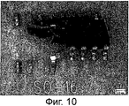
Печатные платы (ПП) используют в электронной промышленности с целью обеспечения механической опоры и электрического соединения электрических и электронных элементов. Печатная плата включает плату или иную подложку, выполненную из изоляционного материала, на котором нанесены токопроводящие дорожки, обычно выполненные из меди. Указанные токопроводящие дорожки выполняют функцию проводов между электрическими элементами, которые на более поздней стадии присоединяют к плате, например, путем пайки. Значительную часть печатных плат изготавливают путем осаждения или иного способа адгезирования слоя меди к плате-подложке, с последующим удалением лишнего количества меди путем химического травления, в результате чего получают медные межсоединения требуемой конфигурации. На этом этапе заготовки печатных плат могут нередко находиться на хранении в течение различных периодов времени, возможно, до нескольких месяцев прежде, чем к печатным платам будут присоединены методом пайки электронные элементы.Printed circuit boards (PCBs) are used in the electronics industry to provide mechanical support and the electrical connection of electrical and electronic elements. A circuit board includes a circuit board or other substrate made of insulating material on which conductive paths, usually made of copper, are applied. These conductive paths serve as wires between electrical elements, which at a later stage are connected to the board, for example, by soldering. A significant part of the printed circuit boards is made by deposition or another method of adhesion of the copper layer to the substrate board, followed by the removal of excess copper by chemical etching, resulting in copper interconnects of the desired configuration. At this stage, blanks of printed circuit boards can often be stored for various periods of time, possibly up to several months before electronic elements are connected to the printed circuit boards by soldering.
Токопроводящие дорожки на печатной плате могут быть выполнены из любого токопроводящего материала. Предпочтительным материалом для токопроводящих дорожек является медь. Медь является предпочтительным материалом для токопроводящих дорожек в основном ввиду своей высокой электропроводности, но, к сожалению, медь легко подвергается окислению на воздухе, в результате чего образуется слой оксида меди, или оксидной пленки на поверхности металла. Указанное окисление является исключительно заметным в случае истечения длительного периода времени между производством заготовки печатной платы и монтажом электрических элементов. Элементы монтируют путем пайки, однако наличие оксидного слоя на медных токопроводящих дорожках может привести к снижению эффективности пайки. В частности, могут возникнуть сухие соединения (непролай), которые имеют тенденцию к отказу во время работы устройства, и слабые соединения с низкой механической прочностью. В ряде случаев соединение вообще не создает электрический контакт. Аналогичные проблемы возникают в том случае, когда токопроводящие дорожки включают иные токопроводящие материалы за исключением меди.Conductive tracks on a printed circuit board can be made of any conductive material. The preferred material for conductive tracks is copper. Copper is the preferred material for conductive paths mainly due to its high electrical conductivity, but unfortunately, copper is easily oxidized in air, resulting in a layer of copper oxide or oxide film on the metal surface. The specified oxidation is extremely noticeable if a long period of time has elapsed between the production of the printed circuit board blank and the installation of electrical elements. The elements are mounted by soldering, however, the presence of an oxide layer on copper conductive paths can lead to a decrease in the efficiency of soldering. In particular, dry joints (non-spill) can occur, which tend to fail during operation of the device, and weak joints with low mechanical strength. In some cases, the connection does not create an electrical contact at all. Similar problems arise when conductive paths include other conductive materials other than copper.
С целью устранения указанных проблем производители печатных плат наносят ряд покрытий, или защитных покрытий на участки, на которых предусматривается проведение пайки. Нередко используют такие металлы, как олово, серебро или сочетание металлов никель-золото. Все без исключения технологические процессы нанесения указанных защитных покрытий являются трудоемкими, при этом требуется использование дополнительного количества металлов, которые в последующем создают угрозу для окружающей среды. Существует возможность нанесения вреда здоровью людей в результате осуществления ряда технологических процессов и использования материалов. Кроме того, некоторые из используемых металлов, таких как золото, являются дорогостоящими. Аналогичный способ предусматривает нанесение покрытий на токопроводящие дорожки, включающих такие органические соединения как бензимидазолы и частицы смачиваемых припоем металлов или припоя (см., например, WO 97/39610), тем самым предотвращая воздействие окислительных условий на токолроводящие дорожки. В процессе пайки органический слой просто удаляют. Обычно указанные органические покрытия не выдерживают многократных циклов нагрева и имеют относительно короткий срок годности до обработки.In order to eliminate these problems, manufacturers of printed circuit boards apply a number of coatings, or protective coatings, to areas where soldering is planned. Often use metals such as tin, silver or a combination of metals nickel-gold. Without exception, all technological processes of applying the indicated protective coatings are labor-intensive, and the use of an additional quantity of metals, which subsequently pose a threat to the environment, is required. There is the possibility of harming human health as a result of a number of technological processes and the use of materials. In addition, some of the metals used, such as gold, are expensive. A similar method involves coating the conductive paths, including organic compounds such as benzimidazoles and particles wettable by solder metals or solder (see, for example, WO 97/39610), thereby preventing oxidizing conditions from affecting the conductive paths. In the process of soldering, the organic layer is simply removed. Typically, these organic coatings do not withstand multiple heating cycles and have a relatively short shelf life before processing.
Очевидно, что способы, применяемые производителями до настоящего времени, являются дорогостоящими либо трудоемкими (включающими дополнительные стадии в технологическом процессе), либо и то и другое, либо ведут к истощению невозобновляемых ресурсов, включая драгоценные металлы. Существует необходимость в более дешевом и (или) более эффективном способе предотвращения окисления токопроводящих дорожек до монтажа электрических элементов путем пайки.Obviously, the methods used by manufacturers to date are expensive or time-consuming (involving additional stages in the process), or both, or lead to the depletion of non-renewable resources, including precious metals. There is a need for a cheaper and (or) more efficient way to prevent the oxidation of conductive tracks before mounting electrical elements by soldering.
Отдельная проблема заключается в том, что печатные платы нередко используют в устройствах, эксплуатируемых в исключительно неблагоприятных условиях и коррозионных средах. В таких условиях токопроводящие дорожки на печатных платах могут подвергаться коррозии, существенно сокращающей срок эксплуатации печатных плат по сравнению со стандартным сроком службы. Такие условия могут возникнуть, например, при использовании устройств в исключительно влажной среде, в которой, в частности, микроскопические капли воды, содержащие такие растворенные газы, как двуокись серы, сероводород, двуокись азота, хлористый водород, хлор, и водяные пары образуют коррозионный раствор. Кроме того, капли влаги могут образовывать тонкую пленку или коррозионные отложения между токопроводящими дорожками на печатных платах, которые могут потенциально вызвать короткое замыкание. В тех случаях, когда производители печатных плат предусматривают создание устройств, используемых в неблагоприятных условиях, они обычно покрывают смонтированные печатные платы однородным покрытием полимера, образующим защитный слой, обеспечивающий защиту от воздействия окружающей среды. Тем не менее, такие покрытия являются дорогостоящими в технологическом плане их нанесения, и для их создания требуются дополнительные этапы в производственном процессе для нанесения покрытия после монтажа печатной платы и в целом дополнительный этап для его последующего удаления. Это также может создать проблемы при переработке поврежденных или вышедших из строя печатных плат, либо в процессе испытания с целью определения их характеристик и выявления неисправностей. Для производителей печатных плат представляет огромный интерес создание более дешевого и (или) более эффективного способа защиты смонтированных печатных плат с экологической точки зрения.A separate problem is that printed circuit boards are often used in devices operating in extremely adverse conditions and corrosive environments. Under such conditions, conductive paths on printed circuit boards can corrode, significantly shortening the useful life of printed circuit boards compared to the standard service life. Such conditions may arise, for example, when using devices in an extremely humid environment, in which, in particular, microscopic drops of water containing dissolved gases such as sulfur dioxide, hydrogen sulfide, nitrogen dioxide, hydrogen chloride, chlorine and water vapor form a corrosive solution . In addition, moisture droplets may form a thin film or corrosive deposits between conductive tracks on printed circuit boards, which can potentially cause a short circuit. In cases where manufacturers of printed circuit boards provide for the creation of devices used in adverse conditions, they usually cover the mounted printed circuit boards with a uniform polymer coating, forming a protective layer that provides protection from environmental influences. However, such coatings are technologically expensive to apply, and to create them requires additional steps in the manufacturing process for coating after installation of the printed circuit board and, in general, an additional step for its subsequent removal. It can also create problems when processing damaged or malfunctioning printed circuit boards, or during the test process to determine their characteristics and identify malfunctions. It is of great interest to manufacturers of printed circuit boards to create a cheaper and (or) more effective way to protect mounted printed circuit boards from an environmental point of view.
Дополнительная проблема, которая может возникнуть после припаивания электронных элементов к печатной плате, заключается в образовании дендритов металлических соединений на паяном соединении. Указанные дендриты могут вызвать сбой смонтированной печатной платы, обусловленный коротким замыканием между контактами. Дендриты представляют собой исключительно мелкие металлические выросты вдоль поверхности, образовавшиеся в результате электромиграции и создающие папоротниковидные структуры. В противоположность «оловянным усам» механизм роста дендритов хорошо изучен, и для их возникновения требуется наличие влаги, создающей металлические ионы, которые далее перераспределяются путем электромиграции в присутствии электромагнитного поля. Покрытие в соответствии с настоящим изобретением обеспечивает защиты против образования дендритов, не позволяя влаги достигнуть поверхности печатной платы, на которой обычно происходит рост дендритов. Покрытие обеспечивает дополнительную защиту, т.к. материалы дендритов характеризуются низкой адгезией к покрытию поверхности, в результате чего снижается образование дендритов между контактами и элементами.An additional problem that can occur after soldering electronic elements to a printed circuit board is the formation of dendrites of metal compounds on a soldered joint. These dendrites can cause a mounted circuit board to fail due to a short circuit between the contacts. Dendrites are extremely small metal outgrowths along the surface, formed as a result of electromigration and creating fern-like structures. In contrast to the “tin mustache,” the dendrite growth mechanism is well understood, and their appearance requires moisture to create metal ions, which are then redistributed by electromigration in the presence of an electromagnetic field. The coating in accordance with the present invention provides protection against the formation of dendrites by preventing moisture from reaching the surface of the printed circuit board, on which dendrite growth usually occurs. The coating provides additional protection, as dendrite materials are characterized by low adhesion to the surface coating, resulting in reduced dendrite formation between contacts and elements.
Настоящее изобретение предусматривает создание печатной платы, на которой выполняют локализованное паяное соединение, при этом на поверхность печатной платы нанесено покрытие, композиция которого включает один или несколько галогенуглеводородных полимеров, состоящее из одного или нескольких слоев с толщиной от монослоя (обычно несколько ангстремов (Å)) до 10 мкм, в которых отсутствует припой, или в основном отсутствует припой между указанной композицией покрытия и токопроводящими дорожками печатной платы. Под полимером понимаются полимеры, образованные на месте из одного или нескольких мономеров, линейных, разветвленных, привитых или сшитых сополимеров, олигомеров, мультиполимеров, мультимономерных полимеров, полимерных смесей, привитых сополимеров, смесей и сплавов полимеров, а также взаимопроникающих полимерных сеток (IPNs).The present invention provides a printed circuit board on which a localized solder joint is made, and a coating is applied to the surface of the printed circuit board, the composition of which includes one or more halogenated hydrocarbons, consisting of one or more layers with a thickness of a monolayer (usually several angstroms (Å)) up to 10 microns, in which there is no solder, or basically no solder between the specified coating composition and the conductive tracks of the printed circuit board. A polymer is understood to mean polymers formed in situ from one or more monomers, linear, branched, grafted or crosslinked copolymers, oligomers, multipolymers, multimonomer polymers, polymer blends, grafted copolymers, polymer blends and alloys, and interpenetrating polymer networks (IPNs).
Толщина покрытия обычно составляет от 1 нм до 2 мкм, более предпочтительно от 1 нм до 500 нм, еще более предпочтительно от 3 нм до 500 нм, еще более предпочтительно от 10 нм до 500 нм и наиболее предпочтительно от 10 нм до 250 нм. Толщина покрытия предпочтительно составляет от 10 нм до 100 нм при различных градиентах, при этом толщина 100 нм является предпочтительной. В другом примере осуществления изобретения толщина покрытия составляет 10 нм - 30 нм. Например, если требуется исключительно высокая стойкость к климатическому воздействию (высокая коррозионная стойкость и износостойкость), можно использовать покрытие большей толщины. Кроме того, толщина покрытия может быть оптимизирована путем создания различной толщины на различных участках на печатной плате в зависимости от того, какие характеристики оптимизируются (например, экологическая защита против электропроводности вдоль оси Z). Толщина покрытия и композиция флюса могут варьироваться с целью оптимизации характеристик защиты от неблагоприятных воздействий окружающей среды и обеспечения исключительно прочных паяных соединений.The coating thickness is usually from 1 nm to 2 μm, more preferably from 1 nm to 500 nm, even more preferably from 3 nm to 500 nm, even more preferably from 10 nm to 500 nm and most preferably from 10 nm to 250 nm. The coating thickness is preferably from 10 nm to 100 nm at various gradients, with a thickness of 100 nm being preferred. In another embodiment, the coating thickness is 10 nm to 30 nm. For example, if extremely high climatic resistance (high corrosion and wear resistance) is required, a thicker coating can be used. In addition, the thickness of the coating can be optimized by creating different thicknesses in different areas on the printed circuit board depending on what characteristics are optimized (for example, environmental protection against electrical conductivity along the Z axis). Coating thickness and flux composition may vary to optimize protection against adverse environmental influences and provide exceptionally strong solder joints.
Галогенуглеводородное покрытие может быть сплошным, в основным сплошным (в частности, на паяемых поверхностях и непаяемых поверхностях между ними или граничащими с ними и, в частности, в основном на всех открытых или уязвимых поверхностях печатной платы), либо несплошным. Для создания исключительно высокого уровня защиты воздействия от окружающей среды может потребоваться в основном сплошное покрытие. Тем не менее, несплошное покрытие может быть достаточным для других целей.The halogen-hydrocarbon coating may be continuous, in the main continuous (in particular, on brazed surfaces and brazed surfaces between them or adjacent to them and, in particular, mainly on all open or vulnerable surfaces of a printed circuit board), or non-continuous. To create an exceptionally high level of environmental protection, a substantially continuous coating may be required. However, an incomplete coating may be sufficient for other purposes.
Под галогенуглеводородным полимером понимается полимер с прямой или разветвленной цепью, либо кольцевой углеродной структурой с 0, 1, 2 или 3 атомами галогена, связанным с каждым атомом углерода в структуре. Атомы галогена могут представлять собой одни и те же галогены (например, фтор) или смесь галогенов (например, фтор и хлор). Термин «галогенуглеводородный полимер» в соответствии со значением, используемым в настоящем контексте, включает полимеры, содержащие одну или несколько ненасыщенных групп, таких как двойные и тройные связи углерод-углерод, и полимер, содержащий один или несколько гетероатомов (атомы, не являющиеся С, Н или галогеном), например, N, S или О. Тем не менее, предпочтительно, чтобы полимер не содержал в основном ненасыщения (так как ненасыщение нередко приводит к снижению устойчивости) и в основном не содержал таких гетероатомов. Предпочтительно, чтобы полимер содержал менее 5% гетероатомов в процентном отношении к общему количеству атомов в полимере. Предпочтительно, чтобы полимер содержал менее 5% двойных или тройных связей углерод-углерод в процентном отношении к общему количеству связей углерод-углерод. Предпочтительно, чтобы молекулярный вес полимера составлял более 1000 атомных единиц массы.By a halogenated hydrocarbon polymer is meant a polymer with a straight or branched chain or a ring carbon structure with 0, 1, 2 or 3 halogen atoms bonded to each carbon atom in the structure. Halogen atoms can be the same halogens (e.g. fluorine) or a mixture of halogens (e.g. fluorine and chlorine). The term “halogenated hydrocarbon polymer” as used in this context includes polymers containing one or more unsaturated groups, such as carbon-carbon double and triple bonds, and a polymer containing one or more heteroatoms (non-C atoms, H or halogen), for example, N, S or O. However, it is preferable that the polymer does not contain mainly unsaturation (since unsaturation often leads to a decrease in stability) and mainly does not contain such heteroatoms. Preferably, the polymer contains less than 5% heteroatoms as a percentage of the total number of atoms in the polymer. Preferably, the polymer contains less than 5% double or triple carbon-carbon bonds as a percentage of the total carbon-carbon bonds. Preferably, the molecular weight of the polymer is more than 1000 atomic mass units.
Полимерные цепи могут быть прямыми или разветвленными, и между полимерными цепями могут образовываться поперечные связи. Галоген может представлять собой фтор, хлор, бром или йод. Предпочтительно, чтобы полимер представлял собой фторуглеводородный полимер, хлоруглеводородный полимер или фторхлоруглеводородный полимер, в котором 0, 1, 2 или 3 атома фтора или хлора связаны в цепи с каждым атомом углерода.The polymer chains can be straight or branched, and cross-links can form between the polymer chains. Halogen may be fluoro, chloro, bromo or iodo. Preferably, the polymer is a fluorocarbon polymer, a chlorohydrocarbon polymer or a fluorocarbon polymer in which 0, 1, 2 or 3 fluorine or chlorine atoms are linked in a chain to each carbon atom.
Примеры предпочтительных примеров осуществления изобретения включают:Examples of preferred embodiments of the invention include:
- ПТФЭ, материалы типа ПТФЭ, фторированные углеводороды, хлорированные фторированные углеводороды, галогенированные углеводороды, галогенуглеводороды или сополимеры, олигомеры, мультиполимеры, мультимономерные полимеры, полимерные смеси, смеси, сплавы, привитые сополимеры с разветвленной цепью, сшитые варианты указанных материалов, а также взаимопроникающие полимерные сетки (ВПС).- PTFE, materials such as PTFE, fluorinated hydrocarbons, chlorinated fluorinated hydrocarbons, halogenated hydrocarbons, halogenated hydrocarbons or copolymers, oligomers, multipolymers, multimeric polymers, polymer mixtures, mixtures, alloys, grafted branched chain copolymers, crosslinked versions of these materials, and also polymer mesh (UPU).
ПХТФЭ (полихлортрифторэтилен) и сополимеры, олигомеры, мультиполимеры, мультимономерные полимеры, полимерные смеси, смеси, сплавы, привитые сополимеры с разветвленной цепью, сшитые варианты указанных материалов, а также взаимопроникающие полимерные сетки (ВПС).PCTFE (polychlorotrifluoroethylene) and copolymers, oligomers, multipolymers, multimeric polymers, polymer mixtures, mixtures, alloys, grafted branched chain copolymers, crosslinked versions of these materials, as well as interpenetrating polymer networks (IPNs).
- ЭПХТФЭ (сополимер этилена и полихлортрифторэтилена) и сополимеры, олигомеры, мультиполимеры, мультимономерные полимеры, полимерные смеси, смеси, сплавы, привитые сополимеры с разветвленной цепью, сшитые варианты указанных материалов, а также взаимопроникающие полимерные сетки (ВПС).- EPHTFE (copolymer of ethylene and polychlorotrifluoroethylene) and copolymers, oligomers, multipolymers, multimeric polymers, polymer mixtures, mixtures, alloys, grafted copolymers with a branched chain, crosslinked versions of these materials, as well as interpenetrating polymer networks (IPNs).
- Иные фторопласты, в том числе указанные ниже материалы и сополимеры, олигомеры, мультиполимеры, мультимономерные полимеры, полимерные смеси, смеси, сплавы, привитые сополимеры с разветвленной цепью, сшитые варианты указанных материалов, а также взаимопроникающие полимерные сетки (ВПС): ЭТФЭ (сополимер этилена и тетрафторэтилена), ФЭП (сополимер тетрафторэтилена и гексафторпропилена), ПФА (сополимер тетрафторэтилена и перфторвинил-эфира), ПВДФ (полимер винилденфторида), ТФЭ (сополимер тетрафторэтилена, гексафторпропилена и винилденфторида), ПВДФГФП (сополимер винилденфторида и гексафторпропилена), МФ(А)Э (сополимер тетрафторэтилена и перфторметилвинил-эфира), ЭФЭП (сополимер этилена, тетрафторэтилена и гексафторпропилена), ГТЭ (сополимер гексафторпропилена, тетрафторэтилена и этилена) и сополимер винилденфторида и хлортрифторэтилена и иные фторопласты.- Other fluoroplastics, including the following materials and copolymers, oligomers, multipolymers, multimeric polymers, polymer mixtures, mixtures, alloys, grafted branched chain copolymers, crosslinked versions of these materials, as well as interpenetrating polymer networks (IPNs): ETFE (copolymer ethylene and tetrafluoroethylene), FEP (copolymer of tetrafluoroethylene and hexafluoropropylene), PFA (copolymer of tetrafluoroethylene and perfluorinated vinyl ether), PVDF (polymer of vinyldenofluoride), TFE (copolymer of tetrafluoroethylene, hexafluoropropylene and vinyldenfluorine yes), PVDFHFP (copolymer of vinylidene fluoride and hexafluoropropylene), MF (A) E (copolymer of tetrafluoroethylene and perfluoromethylvinyl ether), EPEP (copolymer of ethylene, tetrafluoroethylene and hexafluoropropylene), ethylene fluorofluoridethenylene fluorophenyl ethylene fluoride propylene) other fluoroplastics.
Наиболее предпочтительно, чтобы полимер представлял собой материал типа политетрафторэтилена (ПТФЭ) и, в частности, политетрафторэтилен. (ПТФЭ).Most preferably, the polymer is a material such as polytetrafluoroethylene (PTFE) and, in particular, polytetrafluoroethylene. (PTFE).
За счет использования покрытия, в котором галогенуглеводород является высокоразветвленным полимером, сополимером, полимерной комбинацией или полимерной смесью, может быть достигнута более низкая степень смачиваемости.By using a coating in which the halogenated hydrocarbon is a highly branched polymer, copolymer, polymer combination or polymer mixture, a lower degree of wettability can be achieved.
Желательно, чтобы композиция покрытия обладала любым одним или несколькими, предпочтительно всеми нижеприведенными свойствами:It is desirable that the coating composition has any one or more, preferably all of the following properties:
возможность осаждения в виде сплошных пленок, отсутствие трещин, отверстий или дефектов: относительно низкая газовая проницаемость, что обеспечивает достаточную защиту против проникновения газа и против газовой коррозии и окисления «через» покрытие; возможность селективного проведения пайки через покрытие без необходимости его предварительного удаления и создание качественных паяных соединений по сравнению с другими имеющимися в настоящее время защитными покрытиями; возможность выдерживания многократных циклов нагрева; химическая стойкость к коррозионным газам, жидкостям и растворам солей, в частности, к загрязняющим окружающую среду веществам; низкая поверхностная энергия и «смачиваемость»; устойчивость и инертность при нормальной температуры печатной платы; высокие механические свойства, в том числе прочная адгезия к материалам печатной платы и высокая прочность к механическому истиранию: повышенная электростатическая защита, относительно низкая проницаемость жидкостей и растворов солей во избежание жидкостной коррозии «через» покрытие; и в целом не наносить ущерба окружающей среде при ее изготовлении по сравнению с другими существующими технологическими процессами, предназначенными для этой цели.the possibility of deposition in the form of continuous films, the absence of cracks, holes or defects: relatively low gas permeability, which provides sufficient protection against gas penetration and against gas corrosion and oxidation “through” the coating; the possibility of selective soldering through the coating without the need for its preliminary removal and the creation of high-quality soldered joints in comparison with other currently available protective coatings; the ability to withstand multiple heating cycles; chemical resistance to corrosive gases, liquids and salt solutions, in particular, to environmental pollutants; low surface energy and “wettability”; stability and inertness at normal temperature of the printed circuit board; high mechanical properties, including strong adhesion to printed circuit board materials and high mechanical abrasion resistance: increased electrostatic protection, relatively low permeability of liquids and salt solutions to prevent liquid corrosion "through" the coating; and in general, do not harm the environment during its manufacture in comparison with other existing technological processes designed for this purpose.
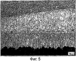
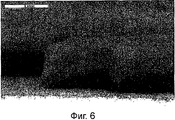
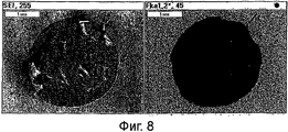
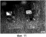
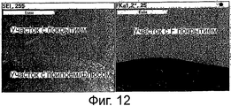
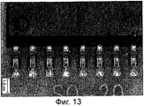
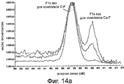
Настоящее изобретение также предусматривает создание иных электрических и (или) электронных устройств либо иных изделий (таких как трубы или иные сантехнические устройства), на которых выполняются паяные соединения и на которые нанесено такое покрытие. Например, настоящее изобретение могло бы быть использовано для нанесения покрытия на оголенные провода (в частности, медные провода), используемые при способах проволочного монтажа. Способ проволочного монтажа представляет собой способ создания межсоединений между интегральной схемой в приборе/кристалле в бескорпусном исполнении и рамкой с выводами внутри интегральной схемы или между прибором/кристаллом в бескорпусном исполнении и печатной платой. В качестве проволоки традиционно использовали золотую или алюминиевую проволоку, но в последнее время особый интерес представляет использование медной проволоки ввиду ряда причин, в том числе ввиду существенного различия стоимости по сравнению с золотой проволокой. При способе проволочного монтажа обычно используют два способа соединений, а именно: термокомпрессионную сварку клинообразным инструментом и термокомпрессионную сварку шариком, при этом при проведении каждого вида сварки используют различное сочетание температуры, давления и ультразвуковой энергии для создания сварки на одном или обоих концах проволоки. С целью достижения прочного соединения сваркой как проволока, так и контактная площадка не должны содержать загрязняющих веществ, в том числе окисных пленок. Стандартной практикой является нанесение золотого защитного покрытия на контактную площадку с целью предотвращения окисления. Покрытие в соответствии с настоящим изобретением на медной контактной площадке также обеспечивает создание неоксидированной поверхности, в результате чего обеспечивается монтаж проволочных межсоединений с применением золотой, алюминиевой или медной проволоки, либо путем термокомпрессионной сварки клинообразным инструментом, либо и термокомпрессионной сварки шариком, однако при существенно более низких затратах по сравнению с нанесением стандартного золотого защитного покрытия на контактную площадку. При использовании медного провода также является эффективным нанесение галогенуглеводородного покрытия на проволоку с целью предотвращения окисления после изготовления проволоки и до ее хранения. Кроме того, галогенуглеводородное покрытие обеспечивает дополнительную защиту от окисления в процессе присоединения сваркой. В другом примере осуществления настоящего изобретения на электроды электронных элементов может быть нанесено покрытие. Полимерное покрытие предпочтительно обеспечивает эффективную защиту от проникновения атмосферных газов и жидкостей, и, что наиболее существенно - кислорода, который обычно реагирует с токопроводящими дорожками, обычно медными токопроводящими дорожками и образует слой оксидной пленки, обычно оксида меди на поверхности токопроводящих дорожек. В результате этого обеспечивается хранение печатной платы с нанесенным покрытием в течение длительного периода времени (до нескольких месяцев или лет), при этом не происходит повреждающего окисления токопроводящих дорожек. Для исследования характера, сплошности и толщины покрытия было использовано формирование изображений методом оптической микроскопии, сканирующей электронной микроскопии и обратного рассеяния электронов. Был использован анализ методом энергетической дисперсии путем проведения рентгеноскопии с целью картографирования уровней и распределения галогенов в покрытии. Измерения активации поверхности и смачиваемости поверхности с использованием растворов химических растворителей указывают на возможность функционирования покрытия в качестве защитного покрытия.The present invention also provides for the creation of other electrical and (or) electronic devices or other products (such as pipes or other plumbing devices) on which solder joints are made and on which such a coating is applied. For example, the present invention could be used to coat bare wires (in particular copper wires) used in wire-mounting methods. The wire mounting method is a method for creating interconnections between an integrated circuit in a device / chip in a package and a frame with terminals inside the integrated circuit or between a device / chip in a package and a circuit board. Gold or aluminum wire has traditionally been used as a wire, but recently, the use of copper wire has been of particular interest due to a number of reasons, including due to the significant difference in cost compared to gold wire. The wire mounting method usually uses two connection methods, namely: thermocompression welding with a wedge-shaped tool and thermocompression welding with a ball, while each type of welding uses a different combination of temperature, pressure and ultrasonic energy to create welding at one or both ends of the wire. In order to achieve a strong welding connection, both the wire and the contact area should not contain pollutants, including oxide films. It is standard practice to apply a gold protective coating to the contact pad to prevent oxidation. The coating in accordance with the present invention on a copper pad also provides a non-oxidized surface, resulting in the installation of wire interconnects using gold, aluminum or copper wire, either by thermocompression welding with a wedge-shaped tool, or thermocompression ball welding, but at significantly lower costs compared to applying a standard gold protective coating to the contact pad. When using copper wire, it is also effective to apply a halogen-hydrocarbon coating to the wire in order to prevent oxidation after the manufacture of the wire and before storage. In addition, a halocarbon coating provides additional protection against oxidation during the welding process. In another embodiment of the present invention, electrodes of electronic elements may be coated. The polymer coating preferably provides effective protection against the ingress of atmospheric gases and liquids, and, most significantly, oxygen, which usually reacts with conductive paths, usually copper conductive paths, and forms a layer of an oxide film, typically copper oxide, on the surface of the conductive paths. As a result of this, the printed circuit board is coated for a long period of time (up to several months or years), without damaging oxidation of the conductive paths. To study the nature, continuity, and thickness of the coating, we used image formation by optical microscopy, scanning electron microscopy, and electron backscattering. An energy dispersion analysis was used by fluoroscopy to map the levels and distribution of halogens in the coating. Measurements of surface activation and surface wettability using chemical solvent solutions indicate that the coating can function as a protective coating.
Если производитель готов к монтажу элементов на заготовке печатной платы, то отсутствует необходимость в очистке печатной платы или в удалении слоя покрытия до начала пайки. Это связано с тем, что используемый галогенуглеводородный полимер обеспечивает создание покрытия, имеющего необычные свойства, позволяющие производить пайку через покрытие и формировать паяное соединение между токопроводящей дорожкой на печатной плате и электрическим элементом. При использовании такого метода пайки обычно необходимо применять флюс. В крайних случаях мог бы быть использован процесс пайки с нагревом для селективного «удаления» покрытия, например, лазерная пайка. В качестве дополнительных альтернативных способов можно использовать сварку, лазерно-стимулированную сварку, ультразвуковую сварку или токопроводящие адгезивы. Дополнительным возможным способом является способ пайки волной припоя, в данном случае для указанного способа может потребоваться селективное флюсование. Используемый припой может представлять собой свинцовый или бессвинцовый припой. В целом не происходит снижения прочности паяного соединения, как могло бы ожидаться, и в некоторых случаях прочность паяного соединения может быть выше по сравнению с прочностью стандартного паяного соединения. Кроме того, в определенных случаях настоящее изобретение позволяет предотвратить образование дендритов на паяных соединениях, в частности, при использовании в бессвинцового припоя.If the manufacturer is ready to mount the elements on the workpiece of the printed circuit board, there is no need to clean the printed circuit board or to remove the coating layer before starting soldering. This is due to the fact that the halogen-hydrocarbon polymer used provides a coating having unusual properties that allow it to solder through the coating and form a solder connection between the conductive track on the printed circuit board and the electrical element. When using this soldering method, flux is usually necessary. In extreme cases, a heat soldering process could be used to selectively “remove” the coating, such as laser soldering. As additional alternative methods, welding, laser-stimulated welding, ultrasonic welding or conductive adhesives can be used. An additional possible method is the method of wave soldering, in this case, the specified method may require selective fluxing. The solder used may be a lead or lead free solder. In general, there is no decrease in the strength of the solder joint, as might be expected, and in some cases, the strength of the solder joint may be higher than the strength of a standard solder joint. In addition, in certain cases, the present invention prevents the formation of dendrites on soldered joints, in particular when used in lead-free solder.
Таким образом, настоящее изобретение предусматривает создание альтернативного способа нанесения защитных покрытий из металлов (таких как олово, серебро, никель и золото) на токопроводящие дорожки печатных плат с целью предотвращения окисления токопроводящих дорожек до проведения пайки. Настоящее изобретение обладает преимуществом в том, что оно основано на недорогостоящем процессе, оно не предусматривает использования токсических металлов, таких как никель, оно является экологически безвредным и характеризуется более высокой безопасностью по сравнению с существующими промышленными технологиями электроосаждения металлов. Настоящее изобретение также упрощает процесс изготовления печатных плат и совместимо с существующими промышленными технологиями пайки. Кроме того, оно обладает дополнительным преимуществом, обеспечивающим «проведение пайки через покрытие», благодаря чему исключается необходимость удаления покрытия до процесса пайки.Thus, the present invention provides an alternative method of applying a protective coating of metals (such as tin, silver, nickel and gold) on the conductive tracks of printed circuit boards in order to prevent oxidation of the conductive tracks before soldering. The present invention has the advantage that it is based on a low-cost process, it does not involve the use of toxic metals such as nickel, it is environmentally friendly and is characterized by higher safety compared to existing industrial metal electrodeposition technologies. The present invention also simplifies the manufacturing process of printed circuit boards and is compatible with existing industrial soldering technologies. In addition, it has the added benefit of “conducting soldering through the coating”, thereby eliminating the need to remove the coating prior to the soldering process.
Дополнительная особенность покрытия из галогенуглеводородного полимера заключается в том, что оно удаляется только на участках, на которые наносят припой и (или) флюс. Таким образом, на участках печатной платы, на которых элементы не присоединяют путем селективной пайки, покрытие не удаляется, тем самым обеспечивая сохранение защитного слоя по поверхности печатной платы и токопроводящих дорожек и создание защиты против коррозии, вызываемой атмосферными газами, такими как двуокись серы, сероводород, двуокись азота, хлористый водород, хлор и водяные пары, и иные коррозионные материалы, в результате чего предотвращается коррозия загрязнителями окружающей среды. Покрытие из галогенуглеводородного полимера также в основном является непроницаемым для жидкостей или коррозионных жидкостей. Следовательно, существует возможность поэтапного монтажа элементов на печатной плате, при этом этапы может разделять существенный период времени - это может создать ряд преимуществ для производителя. Указанное покрытие не разрушается в процессе пайки за исключением участков, на которых производится пайка. Таким образом, на участках, на которых не была проведена пайка, печатную плату можно переработать и (или) доделать путем пайки на более позднем этапе. Кроме того, после завершения монтажа печатной платы непаяные участки печатной платы остаются покрытыми галогенуглеводородным полимером, образующим постоянную защиту против коррозии, вызываемой окружающей средой. Исключается необходимость в проведении дополнительных дорогостоящих этапов нанесения покрытия, такого как однородное покрытие.An additional feature of the halogen-hydrocarbon polymer coating is that it is removed only in areas where solder and / or flux are applied. Thus, in areas of the printed circuit board where the elements are not connected by selective soldering, the coating is not removed, thereby ensuring that the protective layer remains on the surface of the printed circuit board and conductive paths and creates protection against corrosion caused by atmospheric gases such as sulfur dioxide, hydrogen sulfide , nitrogen dioxide, hydrogen chloride, chlorine and water vapor, and other corrosive materials, as a result of which corrosion is prevented by environmental pollutants. The halocarbon polymer coating is also generally impervious to liquids or corrosive liquids. Therefore, there is the possibility of phased installation of elements on a printed circuit board, while the steps can be separated by a significant period of time - this can create a number of advantages for the manufacturer. The specified coating is not destroyed during the soldering process, with the exception of areas where soldering is performed. Thus, in areas where soldering has not been carried out, the printed circuit board can be processed and (or) completed by soldering at a later stage. In addition, after the installation of the printed circuit board is completed, the solder-free sections of the printed circuit board remain coated with a halogen-hydrocarbon polymer, which forms a permanent protection against corrosion caused by the environment. Eliminates the need for additional expensive coating steps, such as a uniform coating.
Токопроводящие дорожки на печатной плате могут включать любой токопроводящий материал. Материалы, из которых могут быть выполнены токопроводящие дорожки, включают металлы, такие как медь, серебро, алюминий или олово, либо токопроводящие полимеры или токопроводящие пасты. Предпочтительным материалом для изготовления токопроводящих дорожек является медь. Токопроводящие полимеры имеют свойство абсорбировать воду и набухать, и, таким образом, нанесение покрытия на токопроводящие полимеры из галогенуглеводородного полимера позволяет предотвратить поглощение воды.The conductive paths on a printed circuit board may include any conductive material. Materials from which conductive paths can be made include metals such as copper, silver, aluminum or tin, or conductive polymers or conductive pastes. The preferred material for the manufacture of conductive tracks is copper. Conductive polymers have the property of absorbing water and swelling, and thus coating the conductive polymers from a halogenated hydrocarbon polymer prevents water absorption.
Еще одна особенность печатной платы с нанесенным покрытием в соответствии с настоящим изобретением заключается в том, что полное сопротивление по вертикальной оси (ось z) является исключительно низким по сравнению с полным сопротивлением по продольной оси (ось х) и поперечной оси (ось у). Под осью z понимается ось, опускающаяся на плоскость печатной платы.Another feature of the coated printed circuit board in accordance with the present invention is that the impedance along the vertical axis (z axis) is exceptionally low compared to the impedance along the longitudinal axis (x axis) and the transverse axis (y axis). The z axis refers to the axis falling onto the plane of the printed circuit board.
Покрытие проявляет высокое полное сопротивление вдоль оси х и оси у, тем самым демонстрируя хорошие изоляционные свойства. Тем не менее, полное сопротивление является относительно низким по оси z. Благодаря этому обеспечивается выполнение электрического контакта через покрытие, не удаляя его. Это создает большие преимущества при создании таких устройств как клавишные панели, контакты переключателей, контрольные точки и т.д. Указанные характеристики могут быть дополнительно оптимизированы путем регулирования свойств покрытия, например, путем регулирования толщины слоя, его композиции и технологических режимов в процессе нанесения покрытия и характера процесса нанесения покрытия.The coating exhibits high impedance along the x axis and y axis, thereby demonstrating good insulating properties. However, the impedance is relatively low along the z axis. This ensures that electrical contact is made through the coating without removing it. This creates great advantages when creating devices such as keypads, switch contacts, breakpoints, etc. These characteristics can be further optimized by adjusting the properties of the coating, for example, by adjusting the thickness of the layer, its composition and process conditions during the coating process and the nature of the coating process.
В целом, настоящее изобретение предотвращает окисление токопроводящих дорожек заготовки печатной платы и (или) иное повреждение под воздействием окружающей среды, например, модулирование термической стойкости, стойкости к царапанию, коррозии и химическому воздействию и создание высокоэффективной защиты токопроводящих дорожек заготовки печатной платы, и обеспечивает защиту смонтированной печатной платы от воздействия окружающей среды с помощью одного первоначального этапа нанесения покрытия из галогенуглеводородного полимера на заготовку печатной платы.In General, the present invention prevents the oxidation of the conductive tracks of the workpiece of the printed circuit board and (or) other damage under the influence of the environment, for example, the modulation of thermal resistance, resistance to scratching, corrosion and chemical attack and the creation of highly effective protection of the conductive tracks of the workpiece of the printed circuit board, and provides protection mounted circuit board from environmental influences using one initial step of coating from a halocarbon polymer on preparation of the printed circuit board.
Изобретение также предусматривает создание способа для защиты печатной платы, включающей создание заготовки печатной платы, имеющей поверхность, подверженную воздействию окружающей среды, при этом на указанной поверхности, подверженной воздействию окружающей среды, отсутствует припой или в основном отсутствует припой, и нанесение на эту поверхность монослоя композиции, содержащей галогенуглеводородный полимер, толщиной (обычно составляющей несколько ангстремов) (Å)) до 10 мкм, с помощью методов освоения тонких пленок, таких как плазменное осаждение, химическое осаждение из паровой фазы, молекулярно-пучковой эпитаксии, создания взаимопроникающих полимерных сеток, поверхностной абсорбции монослоев полимеров мономеров с целью формирования на месте полимеров, полимерных сплавов, либо с помощью напыления. Альтернативными способами осаждения являются плазмостимулированное химическое осаждение из паровой фазы, плазменное осаждение под высоким/атмосферным давлением, химическое осаждение из паровой фазы металлоорганических соединений и лазер-стимулированное химическое осаждение из паровой фазы. Способы нанесения жидкого покрытия, такие как погружение в жидкость, нанесение покрытий путем распыления, нанесение покрытия центрифугированием и (или) золь-гелевые методы нанесения пленок являются дополнительными альтернативными способами.The invention also provides for the creation of a method for protecting a printed circuit board, including creating a blank of a printed circuit board having a surface exposed to the environment, while on the specified surface exposed to the environment, there is no solder or mainly no solder, and a monolayer of the composition is applied to this surface containing a halogenated hydrocarbon polymer with a thickness (typically several angstroms) (Å) of up to 10 μm, using methods for the development of thin films such as plasma Noe deposition, chemical vapor deposition, molecular beam epitaxy, the creation of interpenetrating polymer networks, surface absorption of monolayers of polymers with monomers to form in situ polymers, polymer alloys, or by spraying. Alternative deposition methods are plasma-stimulated chemical vapor deposition, high / atmospheric plasma deposition, organic vapor chemical vapor deposition of organometallic compounds, and laser-stimulated chemical vapor deposition. Liquid coating methods, such as immersion in a liquid, spray coating, centrifugal coating and / or sol-gel film coating methods are additional alternative methods.
Предпочтительный способ может зависеть от толщины требуемого покрытия. Способы нанесения жидкого покрытия могут быть предпочтительными для формирования покрытий большей толщины, в то время как способы плазменного осаждения могут быть предпочтительными для формирования покрытий меньшей толщины. Толщина покрытия обычно составляет от 1 нм до 2 мкм, более предпочтительно от 1 нм до 500 нм, еще более предпочтительно от 3 нм до 500 нм, еще более предпочтительно от 10 нм до 500 нм и наиболее предпочтительно от 10 нм до 250 нм. Толщина покрытия предпочтительно составляет от 10 нм до 100 нм, при этом толщина 100 нм является предпочтительной. Галогенуглеводородный полимер предпочтительно представляет собой фторуглеводородный полимер, хлоруглеводородный полимер или фторхлоруглеводородный полимер, которые также могут содержать микропигменты и небольшое количество иных эксплуатационных добавок (что является широко распространенной практикой в полимерной промышленности) и могут представлять собой, например, материалы типа политетрафторэтилен (ПТФЭ). Предпочтительным способом нанесения галогенуглеводородного полимера на заготовку печатной платы является способ плазменного осаждения, хотя также могут быть применимы все иные вышеперечисленные способы.The preferred method may depend on the thickness of the desired coating. Liquid coating methods may be preferred for the formation of coatings of greater thickness, while plasma deposition methods may be preferred for the formation of coatings of smaller thickness. The coating thickness is usually from 1 nm to 2 μm, more preferably from 1 nm to 500 nm, even more preferably from 3 nm to 500 nm, even more preferably from 10 nm to 500 nm and most preferably from 10 nm to 250 nm. The coating thickness is preferably from 10 nm to 100 nm, with a thickness of 100 nm being preferred. The halocarbon polymer is preferably a fluorocarbon polymer, a chlorocarbon polymer or a fluorocarbon polymer, which may also contain micropigments and a small amount of other operational additives (which is a widespread practice in the polymer industry) and can be, for example, materials such as polytetrafluoroethylene (PTFE). The preferred method for applying a halogenated hydrocarbon polymer to a printed circuit board blank is a plasma deposition method, although all of the other methods mentioned above may also be applicable.
Технологии плазменного осаждения широко используют для осаждения покрытий в различных областях промышленного применения. Указанный способ является эффективным для осаждения сплошных покрытий из тонких пленок с помощью сухой и экологически безвредной технологии. Покрытия наносят на печатные платы в вакуумной камере, в которой создается газовая плазма, содержащая ионизированные газовые ионы, электроны, атомы и нейтральные частицы. При использовании указанного способа печатную плату помещают в вакуумную камеру, в которой сначала создают вакуум при давлении, находящемся обычно в интервале от 10-3 до 10 мбар. Затем в вакуумную камеру подают газ для генерирования стабильной газовой плазмы и далее вводят в плазму одно или несколько соединений-предшественников в виде либо газа, либо жидкости для осуществления процесса осаждения.Plasma deposition technologies are widely used for coating deposition in various industrial applications. This method is effective for the deposition of continuous coatings from thin films using dry and environmentally friendly technology. Coatings are applied to printed circuit boards in a vacuum chamber in which a gas plasma is created containing ionized gas ions, electrons, atoms and neutral particles. Using this method, the printed circuit board is placed in a vacuum chamber, in which a vacuum is first created at a pressure that is usually in the range from 10 −3 to 10 mbar. Then, gas is supplied into the vacuum chamber to generate a stable gas plasma, and then one or more precursor compounds are introduced into the plasma in the form of either gas or liquid to carry out the deposition process.
Соединения-предшественники обычно представляют собой содержащие галогены углеводородные материалы, которые выбирают с целью достижения требуемых свойств покрытия. При введении в газовую плазму соединения-предшественники также ионизируются (разлагаются) и образуют спектр активных частиц, реагирующих на поверхности печатной платы, обычно путем полимеризации, в результате чего образуется тонкое галогенуглеводородное покрытие. Предпочтительными соединениями-предшественниками являются перфторалканы, перфторалкены, перфторалкины, фторалканы, фторалкены, фторалкины, фторхлоралканы, фторхлоралкены, фторхлоралкины или иные фторированные и (или) хлорированные органические материалы (такие как фторуглеводороды, фторуглероды, хлорфторуглеводороды и хлорфторуглероды).Precursor compounds are typically halogen-containing hydrocarbon materials that are selected to achieve the desired coating properties. When introduced into the gas plasma, the precursor compounds also ionize (decompose) and form a spectrum of active particles that react on the surface of the printed circuit board, usually by polymerization, resulting in a thin halogen-hydrocarbon coating. Preferred precursor compounds are perfluoroalkanes, perfluoroalkenes, perfluoroalkines, fluoroalkanes, fluoroalkenes, fluoroalkines, fluorochloroalkanes, fluorochloroalkenes, fluorochloroalkines or other fluorinated and (or) chlorinated organic materials (such as hydrofluorocarbons, chlorofluorocarbons).
В другом аспекте изобретения покрытие на токопроводящей дорожке печатной платы может включать исключительно тонкий слой (например, 5 нм или менее) металлогалоида (предпочтительно фториды металлов, например, фторид меди), непосредственно контактирующий с металлической поверхностью. В одном примере осуществления настоящего изобретения слой металлогалоида может представлять собой монослой или в основном монослой или несколько монослоев, либо включать металлогалоидную зону слоев на поверхности. Такой металлогалоидный слой может быть исключительно прочным и инертным и предотвращать образование оксидных слоев и иных окислов, препятствующих эффективному процессу пайки. Металлогалоидный слой может быть сформирован в том случае, когда активные частицы в газовой плазме реагируют с металлической поверхностью, либо может быть стимулирован с помощью более высокой концентрации частиц фтора. Далее может быть осажден галогенуглеводородный слой в сочетании с металлогалоидным слоем. Два слоя могут быть дискретными в аксиальном и пространственном плане, либо в альтернативном случае может быть создан ступенчатый переход от металлогалоида к галогенуглеводороду. В этом случае металлогалоидный слой защищает металл от окисления, в то время как галогенуглеводородный слой обеспечивает защиту от коррозионных газов и (или) жидкостей окружающей среды, а также защиту от окисления. Кроме того, при износе покрытия, в конечном счете, ввиду механического истирания, нижележащий слой их фторида металла будет препятствовать дальнейшему окислению, обеспечивая тем самым выполнение контакта. Характер и композиция покрытия, сформированного методом плазменного осаждения, зависят от ряда условий, а именно: выбранного плазменного газа; используемого соединения предшественника; давления плазмы; длительности нанесения покрытия: мощности плазмы; конструкции и расположения электродов в камере; подготовки устанавливаемой в камере печатной платы; и размера и геометрии камеры. Обычно технологию плазменного осаждения можно использовать для осаждения тонких пленок толщиной от монослоя (обычно несколько ангстремов (Å)) до 10 микрон (предпочтительно до 5 микрон) в зависимости от вышеприведенных установок и режимов. Плазменная технология как таковая воздействует только на верхнюю поверхность печатной платы и обычно полностью совместима с печатной платой, не повреждая ее и не вызывая иных нежелательных воздействий. Преимущество технологий нанесения плазменных покрытий заключается в том, что осажденное покрытие покрывает все поверхности печатной платы и, таким образом, также будут покрыты вертикальные поверхности, такие как поверхности, доступ к которым обеспечивается только через отверстия в печатной плате, и любые нависающие края. Если на определенный участок печатной платы не предусматривается наносить полимерное покрытие, например, золотые контакты на кромке печатной платы, то в этом случае указанные участки могут быть маскированы при проведении плазменного осаждения.In another aspect of the invention, the coating on the conductive track of a printed circuit board may include an extremely thin layer (e.g., 5 nm or less) of a metal halide (preferably metal fluorides, e.g., copper fluoride) in direct contact with a metal surface. In one embodiment of the present invention, the metal halide layer may be a monolayer or substantially a monolayer or several monolayers, or may include a metal halide layer zone on the surface. Such a metal halide layer can be extremely strong and inert and prevent the formation of oxide layers and other oxides that impede the efficient soldering process. A metal halide layer can be formed when active particles in a gas plasma react with a metal surface, or can be stimulated with a higher concentration of fluorine particles. Further, a halocarbon layer in combination with a metal halide layer may be deposited. Two layers can be discrete in axial and spatial terms, or in the alternative case, a stepwise transition from a metal halide to a halocarbon can be created. In this case, the metal halide layer protects the metal from oxidation, while the halocarbon layer provides protection against corrosive gases and / or environmental fluids, as well as protection against oxidation. In addition, during wear of the coating, ultimately, due to mechanical abrasion, the underlying layer of their metal fluoride will prevent further oxidation, thereby ensuring contact. The nature and composition of the coating formed by plasma deposition depend on a number of conditions, namely: the selected plasma gas; the precursor compound used; plasma pressure; Duration of coating: plasma power; design and arrangement of electrodes in the chamber; preparation of a printed circuit board installed in the chamber; and the size and geometry of the camera. Typically, plasma deposition technology can be used to deposit thin films with a thickness of a monolayer (typically several angstroms (Å)) up to 10 microns (preferably up to 5 microns) depending on the above settings and conditions. Plasma technology as such acts only on the top surface of the printed circuit board and is usually fully compatible with the printed circuit board without damaging it and without causing other undesirable effects. An advantage of plasma coating technologies is that the deposited coating covers all surfaces of the printed circuit board, and thus vertical surfaces, such as surfaces accessible only through openings in the printed circuit board, and any overhanging edges, will also be coated. If it is not intended to apply a polymer coating to a specific area of the printed circuit board, for example, gold contacts on the edge of the printed circuit board, then these areas can be masked during plasma deposition.
В одном варианте плазменной технологии существует возможность использования плазменного способа для очистки in situ поверхности печатной платы до плазменного осаждения с использованием активной газовой плазмы. В этом варианте активную газовую плазму используют обычно в той же самой камере для очистки печатной платы до введения соединения-предшественника для проведения этапа плазменного осаждения. Активная газовая плазма основана на стабильном газе, таком как водород, кислород, азот, аргон, метан, этан, иные углеводороды, тетрафторметан (CF4), гексафторэтан (C2F6), тетрахлорметан (ССЦ), иные фторированные или хлорированные углеводороды, иные редкие газы или их смеси. В одном конкретном примере осуществления в соответствии с настоящим изобретением печатную плату можно было бы очистить тем же самым материалом, который предусматривается осадить на нее в качестве покрытия. Например, фторированные или хлорированные углеводороды, такие как тетрафторметан (CF4) или гексафторэтан (C2F6) или гексафторпропилен (С3F6) или октафторпропан (C3Fs) могли бы быть использованы в плазменном методе как для очистки поверхности печатной платы, так и для осаждения слоя галогенуглеводородного полимеры и (или) слоя фторида (или хлорида) металла.In one embodiment of the plasma technology, it is possible to use a plasma method for in situ cleaning of the surface of a printed circuit board prior to plasma deposition using active gas plasma. In this embodiment, active gas plasma is typically used in the same chamber to clean the circuit board before introducing the precursor compound for the plasma deposition step. Active gas plasma is based on a stable gas, such as hydrogen, oxygen, nitrogen, argon, methane, ethane, other hydrocarbons, tetrafluoromethane (CF 4 ), hexafluoroethane (C 2 F 6 ), carbon tetrachloride (CCC), other fluorinated or chlorinated hydrocarbons, other rare gases or mixtures thereof. In one specific embodiment in accordance with the present invention, the printed circuit board could be cleaned with the same material that is intended to be deposited thereon as a coating. For example, fluorinated or chlorinated hydrocarbons such as tetrafluoromethane (CF 4 ) or hexafluoroethane (C 2 F 6 ) or hexafluoropropylene (C 3 F 6 ) or octafluoropropane (C 3 F s ) could be used in a plasma method as for cleaning the surface of a printed surface boards, and for the deposition of a layer of halocarbon polymers and (or) a layer of fluoride (or chloride) of the metal.
Изобретение также предусматривает создание способа для выполнения соединения с печатной платой, покрытой композицией, включающей галогенуглеводородный полимер, при этом способ включает нанесение припоя и флюса на печатную плату при такой температуре и в течение такого времени, чтобы обеспечивалось соединение припоя с металлом и локальное местное рассеяние и (или) абсорбирование и (или) испарение и (или) растворение и (или) реагирование композиции. Только флюс и повышенная температура в основном воздействуют на галогенуглеводородный полимер для местного удаления покрытия с участка печатной платы, на который нанесен флюс. Температура обычно составляет 200°С-300°С, предпочтительно 240°С-280°С и наиболее предпочтительно 260°С. В одном примере осуществления настоящего изобретения галогенуглеводородный полимер может быть растворен и (или) поглощен флюсом. Было обнаружено, что нередко существует баланс между требуемой температурой и кислотностью или иной агрессивностью флюса. Таким образом, более мягкий флюс может быть достаточным при более высоких температурах и наоборот. В другом примере осуществления настоящего изобретения можно воспользоваться преимуществом эффекта самофлюсования фторида меди на медной поверхности и преимуществом любого разложения полимерного покрытия с высвобождением фтора и (или) фтористого водорода для запуска процесса флюсования (самофлюсования). Наконец, было обнаружено, что в некоторых случаях изобретение позволяет исключить флюс при достаточно высокой температуре и, таким образом, может быть использован локализованный нагрев. Следует отметить, что композиция в основном удаляется только на конкретном участке, на который нанесен припой и (или) флюс и, таким образом, композиция остается присоединенной к поверхности печатной платы вплоть до момента выполнения паяного соединения. Благодаря этому обеспечивается защита токопроводящих дорожек печатной платы от воздействия окружающей среды вплоть до выполнения паяного соединения.The invention also provides for the creation of a method for connecting to a printed circuit board coated with a composition comprising a halogenated hydrocarbon polymer, the method comprising applying solder and flux to the printed circuit board at such a temperature and for such a time that the solder is connected to the metal and local local dispersion is achieved, and (or) absorption and (or) evaporation and (or) dissolution and (or) reaction of the composition. Only flux and elevated temperature mainly affect the halocarbon polymer to locally remove coating from the portion of the printed circuit board on which the flux is applied. The temperature is usually 200 ° C-300 ° C, preferably 240 ° C-280 ° C, and most preferably 260 ° C. In one embodiment of the present invention, the halogenated hydrocarbon polymer may be dissolved and / or absorbed by flux. It was found that often there is a balance between the required temperature and the acidity or other aggressiveness of the flux. Thus, a softer flux may be sufficient at higher temperatures and vice versa. In another embodiment of the present invention, it is possible to take advantage of the self-fluxing effect of copper fluoride on a copper surface and the advantage of any decomposition of the polymer coating with the release of fluorine and (or) hydrogen fluoride to start the fluxing (self-fluxing) process. Finally, it was found that in some cases, the invention eliminates flux at a sufficiently high temperature, and thus, localized heating can be used. It should be noted that the composition is mainly removed only in the specific area on which the solder and (or) flux are applied and, thus, the composition remains attached to the surface of the printed circuit board until the moment of the solder connection. This ensures protection of the conductive tracks of the printed circuit board from environmental influences up to making a solder joint.
Используемый в настоящем изобретении флюс может представлять собой смолу/канифольный флюс, органический флюс, неорганический флюс, флюс, не содержащий галоидных соединений, флюс, не требующий очистки после проведения пайки, безотходный флюс или флюс с низким содержанием твердых частиц. Например, смола/канифольный флюс могли бы представлять собой синтетическую смолу или природную канифоль. Органический флюс мог бы представлять собой, например, органическую кислоту, такую как оксипропионовая кислота или акриловые кислоты; органическую соль, такую как хлорид диметиламмония (DMA HCI); или органический амин, такой как мочевина. Неорганический флюс мог бы представлять собой, например, неорганическую соль, такую как хлорид цинка, хлорид натрия, хлорид калий или фторид натрия; или неорганическую кислоту, такой как соляная кислота или азотная кислота. Примером флюса, не требующего очистки после проведения пайки, является канифольный флюс. Другие типы флюсов, более широко используемые в промышленности, например, для обычной пайки, пайки твердым припоем и сварки, либо для очистки или травления металлических поверхностей (например, тетраборат натрия) также могли бы быть использованы в настоящем изобретении. Флюс, используемый в настоящем способе, обычно представляет собой мягкий флюс, такой как флюс, не требующий проведения последующего этапа очистки печатной платы после пайки. Как вариант, флюс может быть частью паяльной пасты. Выбор флюса может зависеть от характера покрытия, в частности, от толщины и композиции покрытия. Для создания резистивного покрытия большей толщины может потребоваться более агрессивный флюс. Композиция, содержащая активный компонент или компоненты флюса, удаляющие галогенуглеводородную композицию с печатной платы, также могли бы быть использованы вместо флюса в настоящем изобретении.The flux used in the present invention may be a resin / rosin flux, an organic flux, an inorganic flux, a halide-free flux, a flux that does not need to be cleaned after brazing, a waste flux or a low solids flux. For example, the resin / rosin flux could be a synthetic resin or natural rosin. The organic flux could be, for example, an organic acid such as hydroxypropionic acid or acrylic acids; an organic salt such as dimethylammonium chloride (DMA HCI); or an organic amine such as urea. The inorganic flux could be, for example, an inorganic salt such as zinc chloride, sodium chloride, potassium chloride or sodium fluoride; or inorganic acid, such as hydrochloric acid or nitric acid. An example of a flux that does not require cleaning after soldering is rosin flux. Other types of fluxes that are more widely used in industry, for example, for conventional soldering, brazing and welding, or for cleaning or etching metal surfaces (e.g. sodium tetraborate) could also be used in the present invention. The flux used in the present method is typically a soft flux, such as a flux, which does not require a subsequent cleaning step of the circuit board after soldering. Alternatively, the flux may be part of the solder paste. The choice of flux may depend on the nature of the coating, in particular on the thickness and composition of the coating. A more aggressive flux may be required to create a thicker resistive coating. A composition containing an active component or flux components that remove a halogen-hydrocarbon composition from a printed circuit board could also be used instead of the flux in the present invention.
Кроме того, настоящее изобретение предусматривает использование композиции, содержащей галогенуглеводородный полимер для защиты печатной платы от воздействия окружающей среды, на которой выполняют паяное соединение через композицию без ее предварительного удаления путем рассеяния и (или) абсорбции и (или) испарения композиции выборочно в присутствии флюса.In addition, the present invention provides the use of a composition containing a halogenated hydrocarbon polymer to protect the printed circuit board from environmental influences, on which a solder joint is made through the composition without first removing it by scattering and (or) absorption and (or) evaporation of the composition selectively in the presence of flux.
Окружающая среда может содержать газообразные вещества, такие как двуокись серы, сероводород, двуокись азота, хлористый водород, озон или водяные пары или жидкости, такие как вода, т.е. вода, в которой растворены вышеуказанные коррозионные газы, растворы солей или иные утечки. Такие газы обычно присутствуют в сильно загрязненной окружающей среде, например, в городах, сталкивающихся с проблемами загрязнения атмосферного воздуха. Одним конкретным вредным фактором окружающей среды, от которого защищает печатные платы настоящее изобретение, является атмосферная влага, в которой растворены один или несколько вышеперечисленных коррозионных газов. Было обнаружено, что настоящее изобретение также позволяет защитить печатные платы от таких неблагоприятных условий окружающей среды.The environment may contain gaseous substances such as sulfur dioxide, hydrogen sulfide, nitrogen dioxide, hydrogen chloride, ozone or water vapor or liquids such as water, i.e. water in which the above corrosive gases, salt solutions or other leaks are dissolved. Such gases are usually present in highly polluted environments, for example, in cities facing air pollution problems. One particular environmental hazard that the circuit boards of the present invention protects is atmospheric moisture in which one or more of the above corrosive gases are dissolved. It was found that the present invention also protects printed circuit boards from such adverse environmental conditions.
Изобретение также предусматривает использование композиции, содержащей галогенуглеводородный полимер для обеспечения долгосрочной устойчивости при хранении заготовок печатных плат, на которых предусматривается выполнение паяных соединений. Как было указано выше, токопроводящие дорожки на печатных платах имеют свойство подвергаться окислению при воздействии атмосферы. Реакции окисления обычно приводят к образованию окислов металлов при протекании реакции с атмосферным окислением, но они также включают другие реакции окисления, например, в которых медь окисляется, например, до Сu+ или Сu2+. Композиция настоящего изобретения препятствует протеканию указанных реакций окисления, в результате чего заготовки печатных плат могут храниться в течение длительного периода времени без окисления токопроводящих дорожек. Таким образом, после длительного хранения обеспечивается выполнение качественных паяных соединений на печатной плате с использованием стандартных технологий пайки, предпочтительно в присутствии флюса и без каких-либо этапов предварительной очистки печатных плат.The invention also provides for the use of a composition containing a halogenated hydrocarbon polymer to provide long-term storage stability for printed circuit board blanks on which soldered joints are to be made. As mentioned above, conductive tracks on printed circuit boards tend to be oxidized when exposed to the atmosphere. Oxidation reactions usually lead to the formation of metal oxides during the reaction with atmospheric oxidation, but they also include other oxidation reactions, for example, in which copper is oxidized, for example, to Cu + or Cu 2+ . The composition of the present invention prevents the occurrence of these oxidation reactions, as a result of which the blanks of the printed circuit boards can be stored for a long period of time without oxidizing the conductive tracks. Thus, after long-term storage, high-quality soldered joints on the printed circuit board are provided using standard soldering technologies, preferably in the presence of flux and without any preliminary cleaning of the printed circuit boards.
Изобретение также предусматривает использование композиции, содержащей галогенуглеводородный полимер с целью предотвращения окисления и (или) коррозии токопроводящих дорожек заготовки печатной платы до нанесения припоя на токопроводящие дорожки и (или) до формирования паяных соединений.The invention also provides for the use of a composition containing a halogenated hydrocarbon polymer in order to prevent oxidation and / or corrosion of the conductive tracks of the printed circuit board blank before applying solder to the conductive tracks and (or) before the formation of soldered joints.
Описание чертежейDescription of drawings
Фиг.1 - профиль пайки печи для пайки волной припоя, в которой используется промышленная паяльная паста, содержащая свинец.Figure 1 - profile soldering furnace for wave soldering, which uses industrial solder paste containing lead.
Фиг.2 - профиль пайки печи для пайки волной припоя, в которой используется промышленная паяльная паста, не содержащая свинец.Figure 2 is a soldering profile of a wave soldering furnace in which a lead-free industrial solder paste is used.
Фиг.3 - снимок печатной платы с покрытием в соответствии с настоящим изобретением с каплей воды на поверхности, демонстрирующий низкую поверхностную энергию, низкую смачиваемость и непроницаемость для жидкости защитного покрытия.Figure 3 is a snapshot of a coated printed circuit board in accordance with the present invention with a drop of water on the surface, showing low surface energy, low wettability and liquid tightness of the protective coating.
Фиг.4 - вид в поперечном сечении прочного паяного соединения, выполненного через покрытие на печатной плате в соответствии с настоящим изобретением.Figure 4 is a cross-sectional view of a durable solder joint made through a coating on a printed circuit board in accordance with the present invention.
Фиг.5 - снимок поперечного сечения прочного паяного соединения, выполненного на печатной плате в соответствии с настоящим изобретением, демонстрирующий формирование интерметаллических соединений медь-олово высокого качества на верхней стороне нижней медной поверхности.5 is a cross-sectional snapshot of a durable solder joint made on a printed circuit board in accordance with the present invention, showing the formation of high quality copper-tin intermetallic compounds on the upper side of the lower copper surface.
Фиг.6 - изображение, полученное с помощью сканирующей электронной микроскопии кромки с полимерным покрытием толщиной 1 мкм на печатной плате в соответствии с настоящим изобретением при 30000-кратном увеличении.6 is an image obtained by scanning electron microscopy of the edges with a polymer coating with a thickness of 1 μm on a printed circuit board in accordance with the present invention at a magnification of 30,000.
Фиг.7 - изображение в обратно рассеянных электронах, иллюстрирующее пример участка печатной платы с нанесенным покрытием и демонстрирующее сплошность покрытия, превышающую 99,8%.Fig. 7 is a backscattered electron image illustrating an example of a portion of a coated printed circuit board and showing a coating continuity of more than 99.8%.
Фиг.8 - изображение, полученное с помощью сканирующей электронной микроскопии/энергодисперсионного рентгено-спектрального микроанализа, иллюстрирующее участок с выборочно удаленным с печатной платы покрытием под действием флюса и при воздействии температуры при номинальной толщине покрытия в 1 микрон. На изображении слева показан участок, на который был выборочно нанесен флюс. На изображении справа показано, что покрытие было выборочно удалено на участке, на который нанесли флюс.Fig. 8 is an image obtained by scanning electron microscopy / energy dispersive X-ray spectral microanalysis illustrating a portion that is selectively removed from a circuit board by a flux and when exposed to temperature at a nominal coating thickness of 1 micron. The image on the left shows the area where flux was selectively applied. The image on the right shows that the coating was selectively removed in the area where the flux was applied.
Фиг.9 - спектр, полученный методом энергодислерсионного рентгено-спектрального микроанализа, иллюстрирующий углеродную/фтористую композицию покрытия на меди печатной платы в соответствии с настоящим изобретением.Fig. 9 is a spectrum obtained by energy dispersive X-ray spectral microanalysis illustrating a carbon / fluoride copper coating composition of a printed circuit board in accordance with the present invention.
Фиг.10 - изображение выводов элементов интегральной схемы, оторванных от паяной печатной платы в соответствии с настоящим изобретением, демонстрирующее прочность паяных соединений. При проведении жестких испытаний соединения, в конечном счете, разрывались при разрушении связи на участке между медной контактной площадкой и платой-подложкой, а не на участке паяных соединений.Figure 10 - image of the findings of the elements of the integrated circuit, torn from the soldered printed circuit board in accordance with the present invention, showing the strength of the soldered joints. During rigorous testing, the joints were eventually broken when the connection was broken in the area between the copper contact pad and the substrate board, and not in the area of soldered joints.
Фиг.11 - изображение припаянных контактных площадок, оторванных от паяной печатной платы, демонстрирующее прочность паяных соединений. При проведении жестких испытаний соединения, в конечном счете, разрывались при разрушении связи на участке между медной контактной площадкой и платой-подложкой, а не на участке паяных соединений.11 is an image of soldered pads torn from a soldered printed circuit board, showing the strength of soldered joints. During rigorous testing, the joints were eventually broken when the connection was broken in the area between the copper contact pad and the substrate board, and not in the area of soldered joints.
Фиг.12 - изображение, полученное с помощью сканирующей электронной микроскопии/ энергодисперсионного рентгено-спектрального микроанализа, иллюстрирующее наличие полимерного покрытия непосредственно до уровня кромки паяного соединения, выполненного на печатной плате в соответствии с настоящим изобретением.12 is an image obtained by scanning electron microscopy / energy dispersive X-ray spectral microanalysis illustrating the presence of a polymer coating directly to the edge level of the solder joint made on the printed circuit board in accordance with the present invention.
Фиг.13 - изображение оптической микроскопии, иллюстрирующее ряд паяных соединений высокого качества, выполненных на печатной плате.13 is an optical microscopy image illustrating a series of high quality soldered joints made on a printed circuit board.
Фиг.14а - спектр, полученный методом рентгеновской фотоэмиссионной спектроскопии набора тонких покрытий в соответствии с настоящим изобретением, иллюстрирующий различное воздействие материалов C-F и Cu-F.Figa - spectrum obtained by x-ray photoemission spectroscopy of a set of thin coatings in accordance with the present invention, illustrating the different effects of materials C-F and Cu-F.
Фиг.14b - спектр, полученный методом рентгеновской фотоэмиссионной спектроскопии, иллюстрирующий материал, содержащий C-F для нанесения покрытий большой толщины.Fig.14b is a spectrum obtained by x-ray photoemission spectroscopy, illustrating a material containing C-F for coating large thicknesses.
ПРИМЕРЫ EXAMPLES
Изготовление печатных плат с покрытиемCoated PCB Manufacturing
От производителя были получены печатные платы, прошедшие травление и очистку, но на которые не было нанесено защитное покрытие. Указанные платы затем подвергали обработке методом плазменного осаждения для создания, содержащего галоген покрытия. Печатную плату помещали в вакуумную камеру, в которой сначала создавали вакуум при давлении в интервале от 10-3 до 10 мбар. Затем в вакуумную камеру подавали газ для генерирования стабильной газовой плазмы и далее вводил в плазму содержащее галоген углеводородное соединение-предшественник для осуществления процесса осаждения. При введении соединения-предшественника в газовую плазму также происходит его разложение/ионизация с образованием спектра активных частиц, реагирующих на поверхности печатной платы, в результате чего образуется тонкое галогенуглеводородное покрытие. С указанными обработанными печатными платами был проведен ряд экспериментов.From the manufacturer, printed circuit boards were obtained that were etched and cleaned, but which did not have a protective coating. These boards were then subjected to plasma deposition treatment to create a halogen-containing coating. The printed circuit board was placed in a vacuum chamber, in which a vacuum was first created at a pressure in the range from 10 -3 to 10 mbar. Then, gas was supplied into the vacuum chamber to generate a stable gas plasma, and then the halogen-containing hydrocarbon precursor compound was introduced into the plasma to carry out the deposition process. When a precursor compound is introduced into a gas plasma, it also decomposes / ionizes to form a spectrum of active particles that react on the surface of the printed circuit board, resulting in a thin halogen-hydrocarbon coating. With these processed printed circuit boards, a series of experiments were conducted.
Пример 1Example 1
Содержащую свинец промышленную паяльную пасту наносили вручную шприцем на несколько площадок элементов на одной стороне печатной платы.A lead-containing industrial solder paste was applied by hand with a syringe to several element pads on one side of the printed circuit board.
Несколько интегральных схем устанавливали на контактные площадки, на которые была нанесена паяльная паста. Затем печатную плату устанавливали в лечи для пайки волной припоя, в которой был установлен профиль пайки, проиллюстрированный на Фиг.1. Далее проводили визуальный осмотр соединений с помощью микроскопа, и было обнаружено, что они обладают высокими смачивающими характеристиками. К ряду соединений было приложено растягивающее усилие путем подъема элемента с помощью рычага. В каждом случае вывод интегральной схемы выдергивался из припоя, при этом соединение с контактной площадкой оставалось неповрежденным.Several integrated circuits were installed on the contact pads on which the solder paste was applied. Then, the printed circuit board was installed in the lay for soldering with a wave of solder, in which the soldering profile, illustrated in Figure 1, was installed. Next, a visual inspection of the compounds was carried out using a microscope, and it was found that they have high wetting characteristics. A tensile force was applied to a number of joints by lifting the element with a lever. In each case, the output of the integrated circuit was pulled out of the solder, while the connection to the contact pad remained intact.
Пример 2Example 2
Вышеописанное испытание повторяли с использованием бессвинцовой паяльной пасты при измененном профиле пайки волной припоя, как показано на Фиг.2, и получали аналогичные результаты.The above test was repeated using lead-free solder paste with a modified solder wave profile, as shown in FIG. 2, and similar results were obtained.
Пример 3Example 3
Только один флюс наносили на участки двух печатных плат, которые нагревали до 260°С в течение десяти секунд и пяти минут. Осмотр показал, что на покрытие исчезало на участках двух печатных плат, на которые был нанесен флюс. Тем не менее, покрытие сохранялось на участках, на которых не был нанесен флюс.Only one flux was applied to areas of two printed circuit boards, which were heated to 260 ° C for ten seconds and five minutes. Inspection showed that the coating disappeared in areas of two printed circuit boards on which the flux was applied. However, the coating remained in areas where no flux was applied.
Пример 4Example 4
Испытание на предел прочности при сдвигаShear Strength Test
Для испытания на предел прочности было приготовлено восемь сборок с четырьмя финишными покрытиями печатной платы. На каждое финишное покрытие печатной платы приходилось по две сборки. Каждая сборка содержала семь смонтированных бескорпусных резисторов 1206 и четыре бескорпусных конденсаторов 0805. Четырнадцать резисторов 1206 и восемь конденсаторов 0805 из каждого финишного покрытия сборки были подвергнуты испытанию на предел прочности при сдвиге с целью определения максимального сопротивления сдвигу паяных соединений для каждой сборки финишного покрытия.For the tensile strength test, eight assemblies were prepared with four PCB finishes. There were two assemblies for each finish on the printed circuit board. Each assembly contained seven mounted housing resistors 1206 and four housing resistors 0805. Fourteen resistors 1206 and eight capacitors 0805 from each finish of the assembly were subjected to a shear test to determine the maximum shear resistance of soldered joints for each assembly of the finish.
Условия проведения испытанийTest conditions
Печатную плату устанавливали на приборе для определения усилия сдвига. Расстояние установки инструмента над поверхностью печатной платы составляло 80 мкм и ширина инструмента - 2 мкм. При проведении каждого испытания инструмент, создающий сдвиговое усилие, перемещали в направлении вперед с заданной скоростью 100 мкм/секдо контакта с испытуемым элементом, и усилие отслеживали до тех пор, пока не происходил разрыв прикрепления паяного соединения. В качестве прибора для определения сдвига использовали Dage Series 4000 с испытательной головкой DS100.A printed circuit board was installed on the device to determine the shear force. The installation distance of the tool above the surface of the printed circuit board was 80 μm and the tool width was 2 μm. During each test, the shear generating tool was moved forward with a predetermined speed of 100 μm / sec of contact with the test element, and the force was monitored until the attachment of the solder joint was broken. As a shear instrument, a Dage Series 4000 with a DS100 test head was used.
Пример 5Example 5
В таблице ниже поверхностных энергий печатной платы приведено повышение гидрофобности в зависимости от длительности процесса нанесения покрытия:In the table below, the surface energies of the printed circuit board show an increase in hydrophobicity depending on the duration of the coating process:
Claims (5)
Applications Claiming Priority (3)
| Application Number | Priority Date | Filing Date | Title |
|---|---|---|---|
| GB0703172.7 | 2007-02-19 | ||
| GB0703172A GB0703172D0 (en) | 2007-02-19 | 2007-02-19 | Printed circuit boards |
| PCT/GB2008/000552 WO2008102113A2 (en) | 2007-02-19 | 2008-02-18 | Printed circuit boards |
Publications (2)
| Publication Number | Publication Date |
|---|---|
| RU2009130670A RU2009130670A (en) | 2011-04-10 |
| RU2563978C2 true RU2563978C2 (en) | 2015-09-27 |
Family
ID=37908866
Family Applications (1)
| Application Number | Title | Priority Date | Filing Date |
|---|---|---|---|
| RU2009130670/07A RU2563978C2 (en) | 2007-02-19 | 2008-02-18 | Printed-circuit boards |
Country Status (15)
| Country | Link |
|---|---|
| US (2) | US8492898B2 (en) |
| EP (1) | EP2130417B1 (en) |
| JP (3) | JP5558112B2 (en) |
| KR (3) | KR20100014493A (en) |
| CN (1) | CN101682998B (en) |
| AU (1) | AU2008217648B2 (en) |
| CA (1) | CA2678309C (en) |
| DK (1) | DK2130417T3 (en) |
| ES (1) | ES2728309T3 (en) |
| GB (2) | GB0703172D0 (en) |
| PL (1) | PL2130417T3 (en) |
| RU (1) | RU2563978C2 (en) |
| TR (1) | TR201905093T4 (en) |
| TW (1) | TWI462671B (en) |
| WO (1) | WO2008102113A2 (en) |
Cited By (1)
| Publication number | Priority date | Publication date | Assignee | Title |
|---|---|---|---|---|
| RU2717842C2 (en) * | 2015-06-10 | 2020-03-26 | Семблант Лимитед | Coated electrical assembly |
Families Citing this family (29)
| Publication number | Priority date | Publication date | Assignee | Title |
|---|---|---|---|---|
| GB0703172D0 (en) | 2007-02-19 | 2007-03-28 | Pa Knowledge Ltd | Printed circuit boards |
| DE102007062202B4 (en) * | 2007-12-21 | 2021-06-10 | Vitesco Technologies GmbH | Description Process for contacting a rigid circuit board with a contact partner and an arrangement of rigid circuit board and contact partner |
| GB2462824A (en) * | 2008-08-18 | 2010-02-24 | Crombie 123 Ltd | Printed circuit board encapsulation |
| US8618420B2 (en) | 2008-08-18 | 2013-12-31 | Semblant Global Limited | Apparatus with a wire bond and method of forming the same |
| KR101574374B1 (en) * | 2008-08-18 | 2015-12-03 | 셈블란트 리미티드 | Halo-hydrocarbon polymer coating |
| US8701657B2 (en) * | 2008-08-21 | 2014-04-22 | Geno Llc | Systems for generating nitric oxide |
| BE1019159A5 (en) * | 2010-01-22 | 2012-04-03 | Europlasma Nv | METHOD FOR DEPOSITING A EQUIVALENT NANOCOATING BY A LOW-PRESSURE PLASMA PROCESS |
| US8995146B2 (en) | 2010-02-23 | 2015-03-31 | Semblant Limited | Electrical assembly and method |
| GB201003067D0 (en) * | 2010-02-23 | 2010-04-07 | Semblant Ltd | Plasma-polymerized polymer coating |
| GB2485419B (en) * | 2010-11-15 | 2015-02-25 | Semblant Ltd | Method for reducing creep corrosion |
| GB2489761B (en) | 2011-09-07 | 2015-03-04 | Europlasma Nv | Surface coatings |
| CN103379738A (en) * | 2012-04-24 | 2013-10-30 | 镇江华扬信息科技有限公司 | Method for processing surface of printed circuit board |
| US9053405B1 (en) | 2013-08-27 | 2015-06-09 | Flextronics Ap, Llc | Printed RFID circuit |
| US9565748B2 (en) * | 2013-10-28 | 2017-02-07 | Flextronics Ap, Llc | Nano-copper solder for filling thermal vias |
| CN104741490B (en) * | 2013-12-27 | 2017-06-20 | 博世汽车部件(苏州)有限公司 | A kind of soldering appliance |
| US9758889B2 (en) * | 2014-05-08 | 2017-09-12 | Ymt Co., Ltd. | Method for producing substrate formed with copper thin layer, method for manufacturing printed circuit board and printed circuit board manufactured thereby |
| CN104470202B (en) * | 2014-12-31 | 2017-10-24 | 上海创功通讯技术有限公司 | Printed circuit board (PCB) and its bond pad surface processing method for mobile terminal |
| US9516760B2 (en) * | 2015-01-22 | 2016-12-06 | Eastman Kodak Company | Methods for providing electrically-conductive articles |
| CN105386004B (en) * | 2015-10-23 | 2018-11-13 | 衢州顺络电路板有限公司 | Replace the wiring board and its manufacturing method of golden finger |
| US10212825B2 (en) | 2016-03-03 | 2019-02-19 | Motorola Mobility Llc | Polysiloxane films and methods of making polysiloxane films |
| US10351729B2 (en) | 2016-03-03 | 2019-07-16 | Motorola Mobility Llc | Polysiloxane films and methods of making polysiloxane films |
| WO2018013889A1 (en) * | 2016-07-15 | 2018-01-18 | Aculon, Inc | Coated articles that demonstrate push-through electrical connectivity |
| EP3547809B1 (en) * | 2016-11-22 | 2021-10-20 | Senju Metal Industry Co., Ltd | Soldering method |
| GB201621177D0 (en) | 2016-12-13 | 2017-01-25 | Semblant Ltd | Protective coating |
| CN108697001A (en) * | 2017-04-05 | 2018-10-23 | 中国科学院宁波材料技术与工程研究所 | A kind of preparation method of flexible electrode and/or circuit |
| WO2019010122A1 (en) | 2017-07-03 | 2019-01-10 | Avx Corporation | Solid electrolytic capacitor containing a nanocoating |
| JP7275055B2 (en) | 2017-07-03 | 2023-05-17 | キョーセラ・エイブイエックス・コンポーネンツ・コーポレーション | solid electrolytic capacitor assembly |
| CN113275217B (en) * | 2021-05-18 | 2022-06-24 | 佛山市思博睿科技有限公司 | Preparation method of plasma graft copolymerization film layer |
| GB2609034A (en) * | 2021-07-19 | 2023-01-25 | Mordechai Ronen Aviv | Systems and methods for additive manufacturing of electronics |
Citations (3)
| Publication number | Priority date | Publication date | Assignee | Title |
|---|---|---|---|---|
| US3931454A (en) * | 1972-10-17 | 1976-01-06 | Westinghouse Electric Corporation | Printed circuit board and method of preparing it |
| RU2104263C1 (en) * | 1990-06-29 | 1998-02-10 | Эллайд-Сигнал Инк. | Tertiary partially fluorinated alkanes and method or cleaning solid surface |
| RU2177934C2 (en) * | 1994-05-20 | 2002-01-10 | Миннесота Майнинг Энд Мэнюфекчуринг Компани | Omega-hydrofluoroalkyl esters, method of their synthesis, parent carboxylic acids and their derivatives and methods using esters (variants) |
Family Cites Families (164)
| Publication number | Priority date | Publication date | Assignee | Title |
|---|---|---|---|---|
| US3770571A (en) * | 1969-04-02 | 1973-11-06 | Richardson Co | Fabrication of printed circuit boards |
| FR2048044B1 (en) | 1969-06-30 | 1973-01-12 | Fmc Corp | |
| US3649475A (en) * | 1969-07-22 | 1972-03-14 | Gen Dynamics Corp | Multi-layer printed circuit boards and methods of making same |
| US3745536A (en) | 1971-03-01 | 1973-07-10 | Burroughs Corp | High speed serial scan and read-out of keyboards |
| GB1399252A (en) | 1971-05-19 | 1975-07-02 | Post Office | Electrical signal initiating keyboards |
| JPS5219875B2 (en) | 1974-02-07 | 1977-05-31 | ||
| US4136225A (en) * | 1977-07-08 | 1979-01-23 | Bell Telephone Laboratories, Incorporated | Cover coatings for printed circuits |
| JPS5439873A (en) * | 1977-09-06 | 1979-03-27 | Nippon Denso Co | Incombustible ypet flexible printed wiring board |
| US4268568A (en) | 1979-05-14 | 1981-05-19 | Bell Telephone Laboratories, Incorporated | Lubricated electrical contacts |
| JPS5946310B2 (en) * | 1979-08-29 | 1984-11-12 | 株式会社村田製作所 | Method for preventing oxidation of heat-treated copper coatings |
| US4508756A (en) * | 1980-10-08 | 1985-04-02 | Murata Manufacturing Co., Ltd. | Method for inhibiting oxidation of a copper film on ceramic body |
| JPS5766613A (en) * | 1980-10-11 | 1982-04-22 | Murata Manufacturing Co | Method of preventing oxidation of copper coating film on ceramic unit |
| US4369287A (en) * | 1981-03-16 | 1983-01-18 | Motorola Inc. | Permanent fluxing agent and solder-through conformal coating |
| US4531659A (en) * | 1982-02-26 | 1985-07-30 | Wright Hershel E | Foam dispensing device air return system |
| JPS5997029A (en) | 1982-11-26 | 1984-06-04 | Hitachi Ltd | Absolute pressure type semiconductor pressure sensor |
| US4689110A (en) * | 1983-12-22 | 1987-08-25 | Trw Inc. | Method of fabricating multilayer printed circuit board structure |
| US4591659A (en) | 1983-12-22 | 1986-05-27 | Trw Inc. | Multilayer printed circuit board structure |
| JPS60214941A (en) * | 1984-04-10 | 1985-10-28 | 株式会社 潤工社 | Printed substrate |
| JPS60214942A (en) * | 1984-04-10 | 1985-10-28 | 株式会社 潤工社 | Oriented porous ethylene tetrafluoride resin body difficult to be deformed by compression |
| JPS60258232A (en) | 1984-06-04 | 1985-12-20 | Matsushita Electric Works Ltd | Laminated board of fluorine-containing resin |
| JPS60257592A (en) | 1984-06-04 | 1985-12-19 | 松下電工株式会社 | Multilayer printed circuit board |
| US4710429A (en) * | 1985-04-15 | 1987-12-01 | The Dow Chemical Company | Laminates from epoxidized phenol-hydrocarbon adducts |
| JPS61243844A (en) * | 1985-04-23 | 1986-10-30 | Hitachi Ltd | Thermosetting resin composition, laminated sheet and production thereof |
| JPS62252016A (en) * | 1986-04-24 | 1987-11-02 | 富士ポリマテック株式会社 | Formation of continuity part of rubber contact |
| CA1312040C (en) * | 1985-12-19 | 1992-12-29 | Joseph Victor Koleske | Conformal coatings cured with actinic radiation |
| US4732649A (en) * | 1986-06-18 | 1988-03-22 | Macdermid, Incorporated | Method for manufacture of printed circuit boards |
| US4784901A (en) | 1987-04-13 | 1988-11-15 | Japan Gore-Tex, Inc. | Flexible printed circuit board base material |
| US4772509A (en) * | 1987-04-13 | 1988-09-20 | Japan Gore-Tex, Inc. | Printed circuit board base material |
| US4755911A (en) * | 1987-04-28 | 1988-07-05 | Junkosha Co., Ltd. | Multilayer printed circuit board |
| US4797178A (en) | 1987-05-13 | 1989-01-10 | International Business Machines Corporation | Plasma etch enhancement with large mass inert gas |
| JPH01131270A (en) | 1987-11-17 | 1989-05-24 | Asahi Glass Co Ltd | Thermosetting resin composition and laminated board using said composition |
| JPH0180974U (en) | 1987-11-20 | 1989-05-30 | ||
| EP0322097B1 (en) * | 1987-12-17 | 1994-01-05 | Imperial Chemical Industries Plc | Emulsification method and apparatus |
| US6238774B1 (en) * | 1988-02-04 | 2001-05-29 | Fujitsu Limited | Protection of oxide superconductor |
| JPH01225539A (en) | 1988-03-04 | 1989-09-08 | Junkosha Co Ltd | Laminated sheet |
| US4895759A (en) * | 1988-03-18 | 1990-01-23 | Ppg Industries, Inc. | Saturating grade paper |
| US4975319A (en) * | 1988-07-14 | 1990-12-04 | General Electric Company | Printed circuit board from fibers impregnated with epoxy resin mixture, halogenated bisphenol and polyphenylene ether |
| EP0355955A3 (en) | 1988-07-25 | 1991-12-27 | Hitachi, Ltd. | Connection for semiconductor devices or integrated circuits by coated wires and method of manufacturing the same |
| JPH0286675A (en) | 1988-09-22 | 1990-03-27 | Nitto Denko Corp | Fixing material for printed circuit board |
| JPH0826116B2 (en) | 1988-09-30 | 1996-03-13 | 株式会社日立製作所 | Thermosetting resin composition and printed circuit board using the same |
| JPH02120351A (en) | 1988-10-29 | 1990-05-08 | Japan Synthetic Rubber Co Ltd | Flame-retarding resin composition |
| JPH03129796A (en) | 1989-03-23 | 1991-06-03 | Matsushita Electric Works Ltd | Manufacture of printed circuit board |
| JPH0624211B2 (en) | 1989-04-26 | 1994-03-30 | 新日本製鐵株式会社 | Insulation coating bonding wire |
| DE3912580C2 (en) | 1989-04-17 | 1997-08-21 | F&K Delvotec Bondtechnik Gmbh | Bond stamp |
| JPH03242992A (en) | 1990-02-21 | 1991-10-29 | Mitsubishi Plastics Ind Ltd | Manufacture of printed circuit board with curved surface shape |
| US5141702A (en) * | 1990-03-13 | 1992-08-25 | Olin Corporation | Method of making coated electrical connectors |
| JPH03278494A (en) | 1990-03-28 | 1991-12-10 | Toshiba Chem Corp | Printed circuit board |
| JPH07120858B2 (en) | 1990-03-30 | 1995-12-20 | 株式会社日立製作所 | Multilayer printed circuit board and manufacturing method thereof |
| JPH0465184A (en) * | 1990-07-05 | 1992-03-02 | Kansai Paint Co Ltd | Electrodeposition pretreatment method |
| JPH04208597A (en) | 1990-12-01 | 1992-07-30 | Fujitsu Ltd | Multilayer printed circuit board |
| JPH04219901A (en) * | 1990-12-19 | 1992-08-11 | Nippon Steel Corp | Electric parts with protective film |
| EP0498258B1 (en) | 1991-02-07 | 1995-07-26 | Siemens Aktiengesellschaft | Micro multilayer wiring |
| US5274913A (en) * | 1991-10-25 | 1994-01-04 | International Business Machines Corporation | Method of fabricating a reworkable module |
| JP3129796B2 (en) | 1991-11-21 | 2001-01-31 | ニチモウ株式会社 | Cutting method |
| JPH05275487A (en) | 1991-11-22 | 1993-10-22 | Sumitomo 3M Ltd | Electronic parts surface protecting material, electronic parts equipped with the same, and electric connection method of electronic parts using said material |
| JP3242992B2 (en) | 1992-06-17 | 2001-12-25 | パイオニア株式会社 | Organic electroluminescence device |
| JP3348454B2 (en) * | 1993-02-05 | 2002-11-20 | ソニー株式会社 | Antioxidant method |
| JP3552241B2 (en) * | 1993-04-07 | 2004-08-11 | 千住金属工業株式会社 | Pre-flux |
| JP3278494B2 (en) | 1993-06-04 | 2002-04-30 | アクトロニクス株式会社 | How to heat the windings of stationary induction equipment |
| JP3334301B2 (en) | 1993-11-25 | 2002-10-15 | 日本メクトロン株式会社 | Adhesive between fluoroplastic substrate and metal |
| IL111497A (en) * | 1993-12-08 | 2001-01-28 | Rohco Inc Mcgean | Silane compositions useful as adhesives |
| JPH07201502A (en) | 1993-12-28 | 1995-08-04 | Japan Gore Tex Inc | Board mounding type electronic component |
| CA2118544A1 (en) | 1993-12-30 | 1995-07-01 | Henry W. Krautter | Reliability elastomeric keypads and method for making same |
| US5639989A (en) | 1994-04-19 | 1997-06-17 | Motorola Inc. | Shielded electronic component assembly and method for making the same |
| JP2614190B2 (en) | 1994-06-01 | 1997-05-28 | 日本ピラー工業株式会社 | Prepreg for multilayer board, laminated board, multilayer printed circuit board and method of manufacturing the same |
| JPH0827453A (en) | 1994-07-14 | 1996-01-30 | Nitto Denko Corp | Flame-retardant adhesive |
| JP2533747B2 (en) | 1994-07-25 | 1996-09-11 | 株式会社日立製作所 | Laminated board and manufacturing method thereof |
| US5734008A (en) * | 1994-10-28 | 1998-03-31 | Sumitomo Chemical Company, Limited | Polyimide film |
| JPH08143846A (en) | 1994-11-24 | 1996-06-04 | Nitto Denko Corp | Flame-retardant adhesive |
| JPH08288331A (en) | 1995-04-17 | 1996-11-01 | Tanaka Denshi Kogyo Kk | Bonding wire for semiconductor device and production thereof |
| DE19535068C2 (en) * | 1995-09-21 | 1997-08-21 | Lpkf Cad Cam Systeme Gmbh | Coating for the structured production of conductor tracks on the surface of electrically insulating substrates, method for producing the coating and of structured conductor tracks |
| GB9608952D0 (en) | 1995-09-22 | 1996-07-03 | Bnfl Fluorchem Ltd | Coating compositions |
| US7112265B1 (en) | 1996-02-14 | 2006-09-26 | Lifescan Scotland Limited | Disposable test strips with integrated reagent/blood separation layer |
| JP4252631B2 (en) * | 1996-02-29 | 2009-04-08 | 和夫 杉山 | Method for cleaning and modifying surface for solder joint and soldering method |
| AU5561696A (en) * | 1996-04-18 | 1997-11-07 | International Business Machines Corporation | Organic-metallic composite coating for copper surface protection |
| JPH09307219A (en) * | 1996-05-14 | 1997-11-28 | Tamura Seisakusho Co Ltd | Soldering treatment |
| CN1190545C (en) | 1997-06-14 | 2005-02-23 | 英国国防部 | Surface coatings |
| JPH1112716A (en) | 1997-06-19 | 1999-01-19 | Seiko Epson Corp | Material for brazing and its production |
| JPH1131270A (en) | 1997-07-10 | 1999-02-02 | Sanden Corp | Product storage device for automatic vending machine |
| JPH1140907A (en) * | 1997-07-17 | 1999-02-12 | Fuji Photo Film Co Ltd | Printed circuit board and component mounting method thereon |
| US5858074A (en) * | 1997-07-29 | 1999-01-12 | National Research Council Of Canada | Organic solderability preservative compositions |
| JP3420492B2 (en) | 1998-01-23 | 2003-06-23 | 京セラ株式会社 | Semiconductor device |
| JP3551007B2 (en) | 1998-03-02 | 2004-08-04 | セイコーエプソン株式会社 | Wire bonding method and apparatus, and wire bump forming method |
| JP3974256B2 (en) | 1998-04-22 | 2007-09-12 | 新日鐵化学株式会社 | Alkali development type photosensitive resin composition |
| JPH11319635A (en) | 1998-05-15 | 1999-11-24 | Omron Corp | Device for and method of coating organic material to contact point |
| GB9821267D0 (en) | 1998-10-01 | 1998-11-25 | Secr Defence | Surface coatings |
| US6284308B2 (en) * | 1998-12-25 | 2001-09-04 | Victor Company Of Japan, Ltd. | Manufacturing method of printed circuit board |
| JP2000211057A (en) | 1999-01-26 | 2000-08-02 | Hitachi Chem Co Ltd | Intermediate plate for laminate |
| JP2000277654A (en) * | 1999-03-25 | 2000-10-06 | Kokusai Electric Co Ltd | Semiconductor device |
| US6306273B1 (en) * | 1999-04-13 | 2001-10-23 | Aclara Biosciences, Inc. | Methods and compositions for conducting processes in microfluidic devices |
| SG93210A1 (en) * | 1999-06-29 | 2002-12-17 | Univ Singapore | Method for lamination of fluoropolymer to metal and printed circuit board (pcb) substrate |
| JP3640337B2 (en) | 1999-10-04 | 2005-04-20 | 信越化学工業株式会社 | Pressure sensor device |
| JP4343354B2 (en) * | 1999-11-02 | 2009-10-14 | Agcセイミケミカル株式会社 | Solder flux creeping-up inhibitor composition and its use |
| IL132898A (en) * | 1999-11-11 | 2009-09-01 | Nds Ltd | System for bitstream generation |
| EP1889862A1 (en) * | 1999-12-17 | 2008-02-20 | DAICEL CHEMICAL INDUSTRIES, Ltd. | Curable resin composition, process for producing the same, and coated object made with the same |
| US6335224B1 (en) | 2000-05-16 | 2002-01-01 | Sandia Corporation | Protection of microelectronic devices during packaging |
| DE10026714A1 (en) * | 2000-05-30 | 2001-12-13 | Hueck Folien Gmbh | Composite film, process for its production and its use |
| US7465478B2 (en) | 2000-08-11 | 2008-12-16 | Applied Materials, Inc. | Plasma immersion ion implantation process |
| BR0114200B1 (en) * | 2000-10-04 | 2011-05-03 | "Method and apparatus for forming a coating on a substrate". | |
| DE10051053A1 (en) * | 2000-10-14 | 2002-05-02 | Bosch Gmbh Robert | Process for protecting electronic or micromechanical components |
| JP4401049B2 (en) * | 2000-12-11 | 2010-01-20 | 旭硝子株式会社 | Curable composition, cured coating and coated substrate |
| US20020134588A1 (en) | 2000-12-18 | 2002-09-26 | Dollarhite James Michael | Hardsurfacing/hardfacing pertaining primarly to the horizontal directional drilling (HDD) industry utilizing technogenia |
| DE10114897A1 (en) * | 2001-03-26 | 2002-10-24 | Infineon Technologies Ag | Electronic component |
| US6969472B2 (en) | 2001-04-19 | 2005-11-29 | Lsi Logic Corporation | Method of fabricating sub-micron hemispherical and hemicylidrical structures from non-spherically shaped templates |
| JP2002329741A (en) | 2001-05-07 | 2002-11-15 | Sumiden Magnet Wire Kk | Bonding copper wire |
| US6589639B2 (en) * | 2001-05-23 | 2003-07-08 | International Business Machines Corporation | Hole fill composition and method for filling holes in a substrate |
| US6803092B2 (en) * | 2001-06-26 | 2004-10-12 | 3M Innovative Properties Company | Selective deposition of circuit-protective polymers |
| US7195857B2 (en) * | 2001-07-04 | 2007-03-27 | Showa Denko K.K. | Resist curable resin composition and cured article thereof |
| DE10133739A1 (en) | 2001-07-11 | 2003-01-30 | Mewa Textil Service Ag & Co Man Ohg | transport container |
| SG117395A1 (en) | 2001-08-29 | 2005-12-29 | Micron Technology Inc | Wire bonded microelectronic device assemblies and methods of manufacturing same |
| US6500529B1 (en) * | 2001-09-14 | 2002-12-31 | Tonoga, Ltd. | Low signal loss bonding ply for multilayer circuit boards |
| JP4409134B2 (en) * | 2001-10-09 | 2010-02-03 | パナソニック株式会社 | Mounting system |
| TW545092B (en) * | 2001-10-25 | 2003-08-01 | Matsushita Electric Ind Co Ltd | Prepreg and circuit board and method for manufacturing the same |
| JP4075379B2 (en) | 2002-01-08 | 2008-04-16 | 株式会社デンソー | Surface treatment method of fluororesin and method of manufacturing printed wiring board using fluororesin |
| KR100502179B1 (en) * | 2002-02-25 | 2005-08-08 | 스마트알앤씨 주식회사 | Preparation of Metal Clad Laminate for Printed Circuit Board |
| US20030215588A1 (en) | 2002-04-09 | 2003-11-20 | Yeager Gary William | Thermoset composition, method, and article |
| JP4499344B2 (en) | 2002-05-28 | 2010-07-07 | 株式会社日立製作所 | Resin composition and prepreg, laminate and multilayer printed circuit board using the same |
| US6776827B2 (en) | 2002-09-23 | 2004-08-17 | Syed M. Hasan | Method and solution for treating fluorocarbon surfaces |
| JP2004134675A (en) * | 2002-10-11 | 2004-04-30 | Sharp Corp | Soi substrate, manufacturing method thereof and display device |
| JP2004184340A (en) | 2002-12-05 | 2004-07-02 | Tanaka Kikinzoku Kogyo Kk | Manufacturing method of dna probe fixed electrode |
| JP4208597B2 (en) | 2003-02-17 | 2009-01-14 | シャープ株式会社 | Display device, and mobile phone terminal, mobile game terminal, television receiver, and stereoscopic display system using the same |
| JP4020006B2 (en) * | 2003-05-09 | 2007-12-12 | Jsr株式会社 | Insulating resin composition, cured product thereof, and solder joining method |
| EP1505146A1 (en) * | 2003-08-05 | 2005-02-09 | Air Products And Chemicals, Inc. | Processing of substrates with dense fluids comprising acetylenic diols and/or alcohols |
| JP2005112981A (en) | 2003-10-07 | 2005-04-28 | Hitachi Chem Co Ltd | Low-permittivity resin composition, prepreg using the same, metal-clad laminate, and printed circuit board |
| TWI243751B (en) * | 2003-10-21 | 2005-11-21 | Park Electrochemical Corp | Laminates having a low dielectric, low dissipation factor bond core and method of making same |
| JP4896367B2 (en) * | 2003-10-23 | 2012-03-14 | パナソニック株式会社 | Electronic component processing method and apparatus |
| US6923221B2 (en) * | 2003-12-04 | 2005-08-02 | Gilbarco Inc. | Vapor recovery system with ORVR compensation |
| JP4195365B2 (en) | 2003-12-05 | 2008-12-10 | アルプス電気株式会社 | Circuit board with flame resistance and moisture resistance |
| JP4551654B2 (en) | 2003-12-09 | 2010-09-29 | 株式会社神戸製鋼所 | Resin-coated metal plate used for drilling printed circuit boards |
| JP4694251B2 (en) * | 2004-06-10 | 2011-06-08 | 四国化成工業株式会社 | Copper or copper alloy surface treatment agent for lead-free soldering and use thereof |
| US8183386B2 (en) * | 2004-06-10 | 2012-05-22 | Shikoku Chemicals Corporation | Phenylnaphthylimidazole compound and usage of the same |
| DE102004030388A1 (en) * | 2004-06-23 | 2006-01-26 | Ormecon Gmbh | An article with a coating of electrically conductive polymer and process for its preparation |
| US7673970B2 (en) * | 2004-06-30 | 2010-03-09 | Lexmark International, Inc. | Flexible circuit corrosion protection |
| US7648922B2 (en) * | 2004-07-22 | 2010-01-19 | Kyoto University | Fluorocarbon film and method for forming same |
| JP5010112B2 (en) | 2004-07-26 | 2012-08-29 | 新神戸電機株式会社 | Manufacturing method of prepreg, manufacturing method of laminated board and printed wiring board |
| JP4843214B2 (en) | 2004-11-16 | 2011-12-21 | 株式会社東芝 | Module board and disk device |
| US7985677B2 (en) * | 2004-11-30 | 2011-07-26 | Semiconductor Energy Laboratory Co., Ltd. | Method of manufacturing semiconductor device |
| JP4655663B2 (en) * | 2005-02-21 | 2011-03-23 | コニカミノルタオプト株式会社 | Method for producing roll-shaped film having coating layer, roll-shaped optical film, polarizing plate, liquid crystal display device |
| US7579134B2 (en) * | 2005-03-15 | 2009-08-25 | E. I. Dupont De Nemours And Company | Polyimide composite coverlays and methods and compositions relating thereto |
| JP4262699B2 (en) * | 2005-06-22 | 2009-05-13 | 日本航空電子工業株式会社 | Wiring board |
| JP2007010794A (en) | 2005-06-28 | 2007-01-18 | Hitachi Chem Co Ltd | Photosensitive resin composition and photosensitive element |
| JP2007084764A (en) | 2005-09-26 | 2007-04-05 | Jsr Corp | Coating material and method for producing the same |
| JP4722669B2 (en) | 2005-10-26 | 2011-07-13 | 株式会社日立ハイテクインスツルメンツ | Plasma cleaning device |
| JP4438735B2 (en) | 2005-10-31 | 2010-03-24 | 日本ピラー工業株式会社 | Fluorine resin printed circuit board |
| JP2007129039A (en) | 2005-11-02 | 2007-05-24 | Nippon Pillar Packing Co Ltd | Fluorine resin printed circuit board and manufacturing method thereof |
| US20070258722A1 (en) | 2006-05-08 | 2007-11-08 | Jin Yu | Optical receiver |
| JP2007326956A (en) | 2006-06-07 | 2007-12-20 | Kaneka Corp | Prepreg, laminate, and printed circuit board comprising the same |
| US7527915B2 (en) * | 2006-07-19 | 2009-05-05 | E. I. Du Pont De Nemours And Company | Flame retardant multi-layer photoimagable coverlay compositions and methods relating thereto |
| CN101145451B (en) * | 2006-08-29 | 2010-04-14 | 松下电器产业株式会社 | Contact switch |
| US8004860B2 (en) | 2006-08-29 | 2011-08-23 | Texas Instruments Incorporated | Radiofrequency and electromagnetic interference shielding |
| US20090008796A1 (en) | 2006-12-29 | 2009-01-08 | United Test And Assembly Center Ltd. | Copper on organic solderability preservative (osp) interconnect |
| US20080176096A1 (en) | 2007-01-22 | 2008-07-24 | Yen-Hang Cheng | Solderable layer and a method for manufacturing the same |
| GB0703172D0 (en) | 2007-02-19 | 2007-03-28 | Pa Knowledge Ltd | Printed circuit boards |
| KR100882023B1 (en) | 2007-05-25 | 2009-02-05 | 한국생산기술연구원 | Patterning method using surface energy control |
| JP2009051876A (en) | 2007-08-23 | 2009-03-12 | Three M Innovative Properties Co | Coating composition, and article using it |
| TWI377656B (en) | 2007-09-19 | 2012-11-21 | Method for manufacturing packaging substrate | |
| US20090110884A1 (en) | 2007-10-29 | 2009-04-30 | Integrated Surface Technologies | Surface Coating |
| US8618420B2 (en) | 2008-08-18 | 2013-12-31 | Semblant Global Limited | Apparatus with a wire bond and method of forming the same |
| KR101574374B1 (en) | 2008-08-18 | 2015-12-03 | 셈블란트 리미티드 | Halo-hydrocarbon polymer coating |
| TW201041105A (en) | 2009-05-13 | 2010-11-16 | Advanced Semiconductor Eng | Substrate having single patterned metal layer, and package applied with the same, and methods of manufacturing the substrate and package |
| US20110049703A1 (en) | 2009-08-25 | 2011-03-03 | Jun-Chung Hsu | Flip-Chip Package Structure |
| GB201203927D0 (en) | 2012-03-06 | 2012-04-18 | Semblant Ltd | Coated electrical assembly |
| US8995146B2 (en) | 2010-02-23 | 2015-03-31 | Semblant Limited | Electrical assembly and method |
| GB2485419B (en) | 2010-11-15 | 2015-02-25 | Semblant Ltd | Method for reducing creep corrosion |
-
2007
- 2007-02-19 GB GB0703172A patent/GB0703172D0/en not_active Ceased
-
2008
- 2008-02-18 AU AU2008217648A patent/AU2008217648B2/en not_active Ceased
- 2008-02-18 DK DK08709439.7T patent/DK2130417T3/en active
- 2008-02-18 ES ES08709439T patent/ES2728309T3/en active Active
- 2008-02-18 US US12/526,586 patent/US8492898B2/en active Active
- 2008-02-18 CN CN2008800054076A patent/CN101682998B/en active Active
- 2008-02-18 EP EP08709439.7A patent/EP2130417B1/en active Active
- 2008-02-18 WO PCT/GB2008/000552 patent/WO2008102113A2/en active Application Filing
- 2008-02-18 JP JP2009549476A patent/JP5558112B2/en not_active Expired - Fee Related
- 2008-02-18 KR KR20097019604A patent/KR20100014493A/en not_active Application Discontinuation
- 2008-02-18 PL PL08709439T patent/PL2130417T3/en unknown
- 2008-02-18 GB GB0900635A patent/GB2453083B/en not_active Expired - Fee Related
- 2008-02-18 RU RU2009130670/07A patent/RU2563978C2/en not_active IP Right Cessation
- 2008-02-18 KR KR1020157008970A patent/KR20150043557A/en not_active Application Discontinuation
- 2008-02-18 KR KR1020177020884A patent/KR102096147B1/en active IP Right Grant
- 2008-02-18 TR TR2019/05093T patent/TR201905093T4/en unknown
- 2008-02-18 CA CA2678309A patent/CA2678309C/en not_active Expired - Fee Related
- 2008-02-19 TW TW97105763A patent/TWI462671B/en not_active IP Right Cessation
-
2013
- 2013-03-19 JP JP2013056050A patent/JP2013141016A/en active Pending
- 2013-07-22 US US13/947,525 patent/US9648720B2/en active Active
-
2016
- 2016-10-07 JP JP2016199019A patent/JP2017005280A/en active Pending
Patent Citations (3)
| Publication number | Priority date | Publication date | Assignee | Title |
|---|---|---|---|---|
| US3931454A (en) * | 1972-10-17 | 1976-01-06 | Westinghouse Electric Corporation | Printed circuit board and method of preparing it |
| RU2104263C1 (en) * | 1990-06-29 | 1998-02-10 | Эллайд-Сигнал Инк. | Tertiary partially fluorinated alkanes and method or cleaning solid surface |
| RU2177934C2 (en) * | 1994-05-20 | 2002-01-10 | Миннесота Майнинг Энд Мэнюфекчуринг Компани | Omega-hydrofluoroalkyl esters, method of their synthesis, parent carboxylic acids and their derivatives and methods using esters (variants) |
Cited By (1)
| Publication number | Priority date | Publication date | Assignee | Title |
|---|---|---|---|---|
| RU2717842C2 (en) * | 2015-06-10 | 2020-03-26 | Семблант Лимитед | Coated electrical assembly |
Also Published As
| Publication number | Publication date |
|---|---|
| AU2008217648A1 (en) | 2008-08-28 |
| US20130334292A1 (en) | 2013-12-19 |
| CN101682998B (en) | 2012-09-19 |
| CA2678309C (en) | 2016-10-04 |
| PL2130417T3 (en) | 2019-10-31 |
| KR20150043557A (en) | 2015-04-22 |
| EP2130417A2 (en) | 2009-12-09 |
| CN101682998A (en) | 2010-03-24 |
| GB0900635D0 (en) | 2009-02-25 |
| GB2453083B (en) | 2009-08-05 |
| JP2013141016A (en) | 2013-07-18 |
| GB0703172D0 (en) | 2007-03-28 |
| KR20170089979A (en) | 2017-08-04 |
| JP2010519728A (en) | 2010-06-03 |
| RU2009130670A (en) | 2011-04-10 |
| DK2130417T3 (en) | 2019-05-27 |
| JP5558112B2 (en) | 2014-07-23 |
| KR20100014493A (en) | 2010-02-10 |
| KR102096147B1 (en) | 2020-04-01 |
| US8492898B2 (en) | 2013-07-23 |
| WO2008102113A3 (en) | 2008-12-11 |
| US20100025091A1 (en) | 2010-02-04 |
| TW200843590A (en) | 2008-11-01 |
| TWI462671B (en) | 2014-11-21 |
| JP2017005280A (en) | 2017-01-05 |
| TR201905093T4 (en) | 2019-05-21 |
| WO2008102113A2 (en) | 2008-08-28 |
| AU2008217648B2 (en) | 2010-07-29 |
| US9648720B2 (en) | 2017-05-09 |
| GB2453083A (en) | 2009-03-25 |
| CA2678309A1 (en) | 2008-08-28 |
| ES2728309T3 (en) | 2019-10-23 |
| EP2130417B1 (en) | 2019-03-27 |
Similar Documents
| Publication | Publication Date | Title |
|---|---|---|
| RU2563978C2 (en) | Printed-circuit boards | |
| JP5813850B2 (en) | Halohydrocarbon polymer coating | |
| US8618420B2 (en) | Apparatus with a wire bond and method of forming the same | |
| AU2014202320B2 (en) | Halo-hydrocarbon polymer coating |
Legal Events
| Date | Code | Title | Description |
|---|---|---|---|
| FA92 | Acknowledgement of application withdrawn (lack of supplementary materials submitted) |
Effective date: 20130627 |
|
| FZ9A | Application not withdrawn (correction of the notice of withdrawal) |
Effective date: 20140725 |
|
| MM4A | The patent is invalid due to non-payment of fees |
Effective date: 20210219 |