KR20200133377A - 마스크 블랭크, 위상 시프트 마스크 및 반도체 디바이스의 제조 방법 - Google Patents
마스크 블랭크, 위상 시프트 마스크 및 반도체 디바이스의 제조 방법 Download PDFInfo
- Publication number
- KR20200133377A KR20200133377A KR1020207030238A KR20207030238A KR20200133377A KR 20200133377 A KR20200133377 A KR 20200133377A KR 1020207030238 A KR1020207030238 A KR 1020207030238A KR 20207030238 A KR20207030238 A KR 20207030238A KR 20200133377 A KR20200133377 A KR 20200133377A
- Authority
- KR
- South Korea
- Prior art keywords
- phase shift
- film
- layer
- mask
- shift film
- Prior art date
- Legal status (The legal status is an assumption and is not a legal conclusion. Google has not performed a legal analysis and makes no representation as to the accuracy of the status listed.)
- Ceased
Links
- 230000010363 phase shift Effects 0.000 title claims abstract description 473
- 239000004065 semiconductor Substances 0.000 title claims description 31
- 238000004519 manufacturing process Methods 0.000 title claims description 24
- IJGRMHOSHXDMSA-UHFFFAOYSA-N Atomic nitrogen Chemical compound N#N IJGRMHOSHXDMSA-UHFFFAOYSA-N 0.000 claims abstract description 196
- 239000000463 material Substances 0.000 claims abstract description 178
- 229910052710 silicon Inorganic materials 0.000 claims abstract description 118
- 239000010703 silicon Substances 0.000 claims abstract description 118
- QVGXLLKOCUKJST-UHFFFAOYSA-N atomic oxygen Chemical compound [O] QVGXLLKOCUKJST-UHFFFAOYSA-N 0.000 claims abstract description 111
- 229910052760 oxygen Inorganic materials 0.000 claims abstract description 111
- 239000001301 oxygen Substances 0.000 claims abstract description 111
- XUIMIQQOPSSXEZ-UHFFFAOYSA-N Silicon Chemical compound [Si] XUIMIQQOPSSXEZ-UHFFFAOYSA-N 0.000 claims abstract description 110
- 229910052757 nitrogen Inorganic materials 0.000 claims abstract description 96
- 239000000758 substrate Substances 0.000 claims abstract description 91
- 238000002834 transmittance Methods 0.000 claims description 76
- 238000000034 method Methods 0.000 claims description 46
- 238000012546 transfer Methods 0.000 claims description 46
- 229910052755 nonmetal Inorganic materials 0.000 claims description 25
- 229910052751 metal Inorganic materials 0.000 claims description 22
- VYPSYNLAJGMNEJ-UHFFFAOYSA-N Silicium dioxide Chemical compound O=[Si]=O VYPSYNLAJGMNEJ-UHFFFAOYSA-N 0.000 abstract description 42
- 229910052814 silicon oxide Inorganic materials 0.000 abstract description 36
- 229910052581 Si3N4 Inorganic materials 0.000 abstract description 31
- HQVNEWCFYHHQES-UHFFFAOYSA-N silicon nitride Chemical compound N12[Si]34N5[Si]62N3[Si]51N64 HQVNEWCFYHHQES-UHFFFAOYSA-N 0.000 abstract description 31
- 239000010408 film Substances 0.000 description 491
- 239000010410 layer Substances 0.000 description 408
- 230000007547 defect Effects 0.000 description 82
- 239000007789 gas Substances 0.000 description 73
- 238000012937 correction Methods 0.000 description 44
- 238000010894 electron beam technology Methods 0.000 description 43
- 238000005530 etching Methods 0.000 description 34
- 230000008033 biological extinction Effects 0.000 description 30
- 238000001312 dry etching Methods 0.000 description 30
- YCKRFDGAMUMZLT-UHFFFAOYSA-N Fluorine atom Chemical compound [F] YCKRFDGAMUMZLT-UHFFFAOYSA-N 0.000 description 29
- 239000011737 fluorine Substances 0.000 description 29
- 229910052731 fluorine Inorganic materials 0.000 description 29
- 238000011282 treatment Methods 0.000 description 29
- 230000003287 optical effect Effects 0.000 description 28
- 230000000052 comparative effect Effects 0.000 description 26
- 230000008859 change Effects 0.000 description 24
- 239000000460 chlorine Substances 0.000 description 17
- VYZAMTAEIAYCRO-UHFFFAOYSA-N Chromium Chemical compound [Cr] VYZAMTAEIAYCRO-UHFFFAOYSA-N 0.000 description 16
- 239000011651 chromium Substances 0.000 description 16
- 238000010438 heat treatment Methods 0.000 description 16
- 238000001552 radio frequency sputter deposition Methods 0.000 description 16
- 239000010409 thin film Substances 0.000 description 16
- 229910052804 chromium Inorganic materials 0.000 description 14
- 238000004544 sputter deposition Methods 0.000 description 14
- 230000015572 biosynthetic process Effects 0.000 description 13
- 229910052756 noble gas Inorganic materials 0.000 description 13
- ZAMOUSCENKQFHK-UHFFFAOYSA-N Chlorine atom Chemical compound [Cl] ZAMOUSCENKQFHK-UHFFFAOYSA-N 0.000 description 12
- 229910052801 chlorine Inorganic materials 0.000 description 12
- 238000005546 reactive sputtering Methods 0.000 description 12
- LIVNPJMFVYWSIS-UHFFFAOYSA-N silicon monoxide Inorganic materials [Si-]#[O+] LIVNPJMFVYWSIS-UHFFFAOYSA-N 0.000 description 12
- 238000013461 design Methods 0.000 description 11
- XKRFYHLGVUSROY-UHFFFAOYSA-N Argon Chemical compound [Ar] XKRFYHLGVUSROY-UHFFFAOYSA-N 0.000 description 10
- 230000000694 effects Effects 0.000 description 10
- 239000002184 metal Substances 0.000 description 10
- OKTJSMMVPCPJKN-UHFFFAOYSA-N Carbon Chemical compound [C] OKTJSMMVPCPJKN-UHFFFAOYSA-N 0.000 description 9
- 229910052799 carbon Inorganic materials 0.000 description 9
- 239000000203 mixture Substances 0.000 description 9
- YXTPWUNVHCYOSP-UHFFFAOYSA-N bis($l^{2}-silanylidene)molybdenum Chemical compound [Si]=[Mo]=[Si] YXTPWUNVHCYOSP-UHFFFAOYSA-N 0.000 description 8
- 230000001186 cumulative effect Effects 0.000 description 8
- 230000007423 decrease Effects 0.000 description 8
- 229910021344 molybdenum silicide Inorganic materials 0.000 description 8
- 238000004088 simulation Methods 0.000 description 8
- MYMOFIZGZYHOMD-UHFFFAOYSA-N Dioxygen Chemical compound O=O MYMOFIZGZYHOMD-UHFFFAOYSA-N 0.000 description 7
- ZOKXTWBITQBERF-UHFFFAOYSA-N Molybdenum Chemical compound [Mo] ZOKXTWBITQBERF-UHFFFAOYSA-N 0.000 description 7
- 229910004298 SiO 2 Inorganic materials 0.000 description 7
- 229910001882 dioxygen Inorganic materials 0.000 description 7
- 229910052750 molybdenum Inorganic materials 0.000 description 7
- 239000011733 molybdenum Substances 0.000 description 7
- ZOXJGFHDIHLPTG-UHFFFAOYSA-N Boron Chemical compound [B] ZOXJGFHDIHLPTG-UHFFFAOYSA-N 0.000 description 6
- 229910052796 boron Inorganic materials 0.000 description 6
- 238000011161 development Methods 0.000 description 6
- 230000018109 developmental process Effects 0.000 description 6
- 239000001307 helium Substances 0.000 description 6
- 229910052734 helium Inorganic materials 0.000 description 6
- SWQJXJOGLNCZEY-UHFFFAOYSA-N helium atom Chemical compound [He] SWQJXJOGLNCZEY-UHFFFAOYSA-N 0.000 description 6
- FFUAGWLWBBFQJT-UHFFFAOYSA-N hexamethyldisilazane Chemical compound C[Si](C)(C)N[Si](C)(C)C FFUAGWLWBBFQJT-UHFFFAOYSA-N 0.000 description 6
- 229910052786 argon Inorganic materials 0.000 description 5
- 230000005540 biological transmission Effects 0.000 description 5
- 239000011521 glass Substances 0.000 description 5
- 238000007689 inspection Methods 0.000 description 5
- 229910052743 krypton Inorganic materials 0.000 description 5
- DNNSSWSSYDEUBZ-UHFFFAOYSA-N krypton atom Chemical compound [Kr] DNNSSWSSYDEUBZ-UHFFFAOYSA-N 0.000 description 5
- 239000011368 organic material Substances 0.000 description 5
- 230000008569 process Effects 0.000 description 5
- GUVRBAGPIYLISA-UHFFFAOYSA-N tantalum atom Chemical compound [Ta] GUVRBAGPIYLISA-UHFFFAOYSA-N 0.000 description 5
- 229910052723 transition metal Inorganic materials 0.000 description 5
- 150000003624 transition metals Chemical class 0.000 description 5
- 238000004833 X-ray photoelectron spectroscopy Methods 0.000 description 4
- 238000012545 processing Methods 0.000 description 4
- 239000002356 single layer Substances 0.000 description 4
- 238000004528 spin coating Methods 0.000 description 4
- 229910052715 tantalum Inorganic materials 0.000 description 4
- UFHFLCQGNIYNRP-UHFFFAOYSA-N Hydrogen Chemical compound [H][H] UFHFLCQGNIYNRP-UHFFFAOYSA-N 0.000 description 3
- PXHVJJICTQNCMI-UHFFFAOYSA-N Nickel Chemical compound [Ni] PXHVJJICTQNCMI-UHFFFAOYSA-N 0.000 description 3
- KDLHZDBZIXYQEI-UHFFFAOYSA-N Palladium Chemical compound [Pd] KDLHZDBZIXYQEI-UHFFFAOYSA-N 0.000 description 3
- OAICVXFJPJFONN-UHFFFAOYSA-N Phosphorus Chemical compound [P] OAICVXFJPJFONN-UHFFFAOYSA-N 0.000 description 3
- BUGBHKTXTAQXES-UHFFFAOYSA-N Selenium Chemical compound [Se] BUGBHKTXTAQXES-UHFFFAOYSA-N 0.000 description 3
- NINIDFKCEFEMDL-UHFFFAOYSA-N Sulfur Chemical compound [S] NINIDFKCEFEMDL-UHFFFAOYSA-N 0.000 description 3
- 229910052787 antimony Inorganic materials 0.000 description 3
- WATWJIUSRGPENY-UHFFFAOYSA-N antimony atom Chemical compound [Sb] WATWJIUSRGPENY-UHFFFAOYSA-N 0.000 description 3
- 238000004140 cleaning Methods 0.000 description 3
- 229910052732 germanium Inorganic materials 0.000 description 3
- GNPVGFCGXDBREM-UHFFFAOYSA-N germanium atom Chemical compound [Ge] GNPVGFCGXDBREM-UHFFFAOYSA-N 0.000 description 3
- 229910052736 halogen Inorganic materials 0.000 description 3
- 150000002367 halogens Chemical class 0.000 description 3
- 229910052739 hydrogen Inorganic materials 0.000 description 3
- 239000001257 hydrogen Substances 0.000 description 3
- 230000009545 invasion Effects 0.000 description 3
- 238000000059 patterning Methods 0.000 description 3
- 229910052698 phosphorus Inorganic materials 0.000 description 3
- 239000011574 phosphorus Substances 0.000 description 3
- 229910052711 selenium Inorganic materials 0.000 description 3
- 239000011669 selenium Substances 0.000 description 3
- 235000012239 silicon dioxide Nutrition 0.000 description 3
- 239000000377 silicon dioxide Substances 0.000 description 3
- 238000005477 sputtering target Methods 0.000 description 3
- 229910052717 sulfur Inorganic materials 0.000 description 3
- 239000011593 sulfur Substances 0.000 description 3
- 239000002344 surface layer Substances 0.000 description 3
- 230000003746 surface roughness Effects 0.000 description 3
- 229910052714 tellurium Inorganic materials 0.000 description 3
- PORWMNRCUJJQNO-UHFFFAOYSA-N tellurium atom Chemical compound [Te] PORWMNRCUJJQNO-UHFFFAOYSA-N 0.000 description 3
- CURLTUGMZLYLDI-UHFFFAOYSA-N Carbon dioxide Chemical compound O=C=O CURLTUGMZLYLDI-UHFFFAOYSA-N 0.000 description 2
- 229910018557 Si O Inorganic materials 0.000 description 2
- 229910007991 Si-N Inorganic materials 0.000 description 2
- 229910006294 Si—N Inorganic materials 0.000 description 2
- ATJFFYVFTNAWJD-UHFFFAOYSA-N Tin Chemical compound [Sn] ATJFFYVFTNAWJD-UHFFFAOYSA-N 0.000 description 2
- 238000004458 analytical method Methods 0.000 description 2
- 239000000470 constituent Substances 0.000 description 2
- 238000001659 ion-beam spectroscopy Methods 0.000 description 2
- 238000003475 lamination Methods 0.000 description 2
- 238000002156 mixing Methods 0.000 description 2
- 239000010955 niobium Substances 0.000 description 2
- 238000000206 photolithography Methods 0.000 description 2
- 230000007261 regionalization Effects 0.000 description 2
- 239000010948 rhodium Substances 0.000 description 2
- 239000010936 titanium Substances 0.000 description 2
- 238000005406 washing Methods 0.000 description 2
- ITWBWJFEJCHKSN-UHFFFAOYSA-N 1,4,7-triazonane Chemical compound C1CNCCNCCN1 ITWBWJFEJCHKSN-UHFFFAOYSA-N 0.000 description 1
- BLIQUJLAJXRXSG-UHFFFAOYSA-N 1-benzyl-3-(trifluoromethyl)pyrrolidin-1-ium-3-carboxylate Chemical compound C1C(C(=O)O)(C(F)(F)F)CCN1CC1=CC=CC=C1 BLIQUJLAJXRXSG-UHFFFAOYSA-N 0.000 description 1
- KRHYYFGTRYWZRS-UHFFFAOYSA-M Fluoride anion Chemical compound [F-] KRHYYFGTRYWZRS-UHFFFAOYSA-M 0.000 description 1
- KJTLSVCANCCWHF-UHFFFAOYSA-N Ruthenium Chemical compound [Ru] KJTLSVCANCCWHF-UHFFFAOYSA-N 0.000 description 1
- 229910008045 Si-Si Inorganic materials 0.000 description 1
- 229910004541 SiN Inorganic materials 0.000 description 1
- 229910006411 Si—Si Inorganic materials 0.000 description 1
- 229910004535 TaBN Inorganic materials 0.000 description 1
- 229910004166 TaN Inorganic materials 0.000 description 1
- 229910003071 TaON Inorganic materials 0.000 description 1
- 229910010413 TiO 2 Inorganic materials 0.000 description 1
- RTAQQCXQSZGOHL-UHFFFAOYSA-N Titanium Chemical compound [Ti] RTAQQCXQSZGOHL-UHFFFAOYSA-N 0.000 description 1
- 229910045601 alloy Inorganic materials 0.000 description 1
- 239000000956 alloy Substances 0.000 description 1
- 239000005354 aluminosilicate glass Substances 0.000 description 1
- 230000008901 benefit Effects 0.000 description 1
- 229910002092 carbon dioxide Inorganic materials 0.000 description 1
- 239000001569 carbon dioxide Substances 0.000 description 1
- 239000013078 crystal Substances 0.000 description 1
- 230000003247 decreasing effect Effects 0.000 description 1
- 238000001514 detection method Methods 0.000 description 1
- 238000001035 drying Methods 0.000 description 1
- 230000002349 favourable effect Effects 0.000 description 1
- 229910052735 hafnium Inorganic materials 0.000 description 1
- VBJZVLUMGGDVMO-UHFFFAOYSA-N hafnium atom Chemical compound [Hf] VBJZVLUMGGDVMO-UHFFFAOYSA-N 0.000 description 1
- 230000001678 irradiating effect Effects 0.000 description 1
- 238000005259 measurement Methods 0.000 description 1
- 150000002739 metals Chemical class 0.000 description 1
- 238000009740 moulding (composite fabrication) Methods 0.000 description 1
- 229910052754 neon Inorganic materials 0.000 description 1
- GKAOGPIIYCISHV-UHFFFAOYSA-N neon atom Chemical compound [Ne] GKAOGPIIYCISHV-UHFFFAOYSA-N 0.000 description 1
- 229910052759 nickel Inorganic materials 0.000 description 1
- 229910052758 niobium Inorganic materials 0.000 description 1
- GUCVJGMIXFAOAE-UHFFFAOYSA-N niobium atom Chemical compound [Nb] GUCVJGMIXFAOAE-UHFFFAOYSA-N 0.000 description 1
- 150000004767 nitrides Chemical class 0.000 description 1
- QJGQUHMNIGDVPM-UHFFFAOYSA-N nitrogen group Chemical group [N] QJGQUHMNIGDVPM-UHFFFAOYSA-N 0.000 description 1
- 150000002835 noble gases Chemical class 0.000 description 1
- 229910052763 palladium Inorganic materials 0.000 description 1
- 239000002245 particle Substances 0.000 description 1
- 230000000737 periodic effect Effects 0.000 description 1
- 238000009832 plasma treatment Methods 0.000 description 1
- 230000001681 protective effect Effects 0.000 description 1
- 230000009467 reduction Effects 0.000 description 1
- 229910052703 rhodium Inorganic materials 0.000 description 1
- MHOVAHRLVXNVSD-UHFFFAOYSA-N rhodium atom Chemical compound [Rh] MHOVAHRLVXNVSD-UHFFFAOYSA-N 0.000 description 1
- 229910052707 ruthenium Inorganic materials 0.000 description 1
- VSZWPYCFIRKVQL-UHFFFAOYSA-N selanylidenegallium;selenium Chemical compound [Se].[Se]=[Ga].[Se]=[Ga] VSZWPYCFIRKVQL-UHFFFAOYSA-N 0.000 description 1
- 150000003377 silicon compounds Chemical class 0.000 description 1
- 239000005361 soda-lime glass Substances 0.000 description 1
- 229910052719 titanium Inorganic materials 0.000 description 1
- WFKWXMTUELFFGS-UHFFFAOYSA-N tungsten Chemical compound [W] WFKWXMTUELFFGS-UHFFFAOYSA-N 0.000 description 1
- 229910052721 tungsten Inorganic materials 0.000 description 1
- 239000010937 tungsten Substances 0.000 description 1
- 238000009281 ultraviolet germicidal irradiation Methods 0.000 description 1
- LEONUFNNVUYDNQ-UHFFFAOYSA-N vanadium atom Chemical compound [V] LEONUFNNVUYDNQ-UHFFFAOYSA-N 0.000 description 1
- 229910052724 xenon Inorganic materials 0.000 description 1
- FHNFHKCVQCLJFQ-UHFFFAOYSA-N xenon atom Chemical compound [Xe] FHNFHKCVQCLJFQ-UHFFFAOYSA-N 0.000 description 1
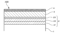
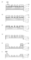
Images
Classifications
-
- G—PHYSICS
- G03—PHOTOGRAPHY; CINEMATOGRAPHY; ANALOGOUS TECHNIQUES USING WAVES OTHER THAN OPTICAL WAVES; ELECTROGRAPHY; HOLOGRAPHY
- G03F—PHOTOMECHANICAL PRODUCTION OF TEXTURED OR PATTERNED SURFACES, e.g. FOR PRINTING, FOR PROCESSING OF SEMICONDUCTOR DEVICES; MATERIALS THEREFOR; ORIGINALS THEREFOR; APPARATUS SPECIALLY ADAPTED THEREFOR
- G03F1/00—Originals for photomechanical production of textured or patterned surfaces, e.g., masks, photo-masks, reticles; Mask blanks or pellicles therefor; Containers specially adapted therefor; Preparation thereof
- G03F1/68—Preparation processes not covered by groups G03F1/20 - G03F1/50
- G03F1/80—Etching
-
- G—PHYSICS
- G03—PHOTOGRAPHY; CINEMATOGRAPHY; ANALOGOUS TECHNIQUES USING WAVES OTHER THAN OPTICAL WAVES; ELECTROGRAPHY; HOLOGRAPHY
- G03F—PHOTOMECHANICAL PRODUCTION OF TEXTURED OR PATTERNED SURFACES, e.g. FOR PRINTING, FOR PROCESSING OF SEMICONDUCTOR DEVICES; MATERIALS THEREFOR; ORIGINALS THEREFOR; APPARATUS SPECIALLY ADAPTED THEREFOR
- G03F1/00—Originals for photomechanical production of textured or patterned surfaces, e.g., masks, photo-masks, reticles; Mask blanks or pellicles therefor; Containers specially adapted therefor; Preparation thereof
- G03F1/26—Phase shift masks [PSM]; PSM blanks; Preparation thereof
- G03F1/32—Attenuating PSM [att-PSM], e.g. halftone PSM or PSM having semi-transparent phase shift portion; Preparation thereof
-
- G—PHYSICS
- G03—PHOTOGRAPHY; CINEMATOGRAPHY; ANALOGOUS TECHNIQUES USING WAVES OTHER THAN OPTICAL WAVES; ELECTROGRAPHY; HOLOGRAPHY
- G03F—PHOTOMECHANICAL PRODUCTION OF TEXTURED OR PATTERNED SURFACES, e.g. FOR PRINTING, FOR PROCESSING OF SEMICONDUCTOR DEVICES; MATERIALS THEREFOR; ORIGINALS THEREFOR; APPARATUS SPECIALLY ADAPTED THEREFOR
- G03F1/00—Originals for photomechanical production of textured or patterned surfaces, e.g., masks, photo-masks, reticles; Mask blanks or pellicles therefor; Containers specially adapted therefor; Preparation thereof
- G03F1/54—Absorbers, e.g. of opaque materials
- G03F1/58—Absorbers, e.g. of opaque materials having two or more different absorber layers, e.g. stacked multilayer absorbers
-
- G—PHYSICS
- G03—PHOTOGRAPHY; CINEMATOGRAPHY; ANALOGOUS TECHNIQUES USING WAVES OTHER THAN OPTICAL WAVES; ELECTROGRAPHY; HOLOGRAPHY
- G03F—PHOTOMECHANICAL PRODUCTION OF TEXTURED OR PATTERNED SURFACES, e.g. FOR PRINTING, FOR PROCESSING OF SEMICONDUCTOR DEVICES; MATERIALS THEREFOR; ORIGINALS THEREFOR; APPARATUS SPECIALLY ADAPTED THEREFOR
- G03F1/00—Originals for photomechanical production of textured or patterned surfaces, e.g., masks, photo-masks, reticles; Mask blanks or pellicles therefor; Containers specially adapted therefor; Preparation thereof
- G03F1/68—Preparation processes not covered by groups G03F1/20 - G03F1/50
- G03F1/72—Repair or correction of mask defects
-
- G—PHYSICS
- G03—PHOTOGRAPHY; CINEMATOGRAPHY; ANALOGOUS TECHNIQUES USING WAVES OTHER THAN OPTICAL WAVES; ELECTROGRAPHY; HOLOGRAPHY
- G03F—PHOTOMECHANICAL PRODUCTION OF TEXTURED OR PATTERNED SURFACES, e.g. FOR PRINTING, FOR PROCESSING OF SEMICONDUCTOR DEVICES; MATERIALS THEREFOR; ORIGINALS THEREFOR; APPARATUS SPECIALLY ADAPTED THEREFOR
- G03F1/00—Originals for photomechanical production of textured or patterned surfaces, e.g., masks, photo-masks, reticles; Mask blanks or pellicles therefor; Containers specially adapted therefor; Preparation thereof
- G03F1/68—Preparation processes not covered by groups G03F1/20 - G03F1/50
- G03F1/82—Auxiliary processes, e.g. cleaning or inspecting
- G03F1/84—Inspecting
-
- H—ELECTRICITY
- H01—ELECTRIC ELEMENTS
- H01L—SEMICONDUCTOR DEVICES NOT COVERED BY CLASS H10
- H01L21/00—Processes or apparatus adapted for the manufacture or treatment of semiconductor or solid state devices or of parts thereof
- H01L21/02—Manufacture or treatment of semiconductor devices or of parts thereof
- H01L21/027—Making masks on semiconductor bodies for further photolithographic processing not provided for in group H01L21/18 or H01L21/34
- H01L21/033—Making masks on semiconductor bodies for further photolithographic processing not provided for in group H01L21/18 or H01L21/34 comprising inorganic layers
- H01L21/0334—Making masks on semiconductor bodies for further photolithographic processing not provided for in group H01L21/18 or H01L21/34 comprising inorganic layers characterised by their size, orientation, disposition, behaviour, shape, in horizontal or vertical plane
- H01L21/0337—Making masks on semiconductor bodies for further photolithographic processing not provided for in group H01L21/18 or H01L21/34 comprising inorganic layers characterised by their size, orientation, disposition, behaviour, shape, in horizontal or vertical plane characterised by the process involved to create the mask, e.g. lift-off masks, sidewalls, or to modify the mask, e.g. pre-treatment, post-treatment
Landscapes
- Physics & Mathematics (AREA)
- General Physics & Mathematics (AREA)
- Engineering & Computer Science (AREA)
- Chemical & Material Sciences (AREA)
- Inorganic Chemistry (AREA)
- Condensed Matter Physics & Semiconductors (AREA)
- Manufacturing & Machinery (AREA)
- Computer Hardware Design (AREA)
- Microelectronics & Electronic Packaging (AREA)
- Power Engineering (AREA)
- Preparing Plates And Mask In Photomechanical Process (AREA)
Applications Claiming Priority (3)
| Application Number | Priority Date | Filing Date | Title |
|---|---|---|---|
| JPJP-P-2018-058004 | 2018-03-26 | ||
| JP2018058004 | 2018-03-26 | ||
| PCT/JP2019/010772 WO2019188397A1 (ja) | 2018-03-26 | 2019-03-15 | マスクブランク、位相シフトマスク及び半導体デバイスの製造方法 |
Publications (1)
| Publication Number | Publication Date |
|---|---|
| KR20200133377A true KR20200133377A (ko) | 2020-11-27 |
Family
ID=68058151
Family Applications (1)
| Application Number | Title | Priority Date | Filing Date |
|---|---|---|---|
| KR1020207030238A Ceased KR20200133377A (ko) | 2018-03-26 | 2019-03-15 | 마스크 블랭크, 위상 시프트 마스크 및 반도체 디바이스의 제조 방법 |
Country Status (7)
| Country | Link |
|---|---|
| US (1) | US20210026235A1 (enExample) |
| JP (1) | JP7201502B2 (enExample) |
| KR (1) | KR20200133377A (enExample) |
| CN (1) | CN111902772A (enExample) |
| SG (1) | SG11202009172VA (enExample) |
| TW (1) | TWI854972B (enExample) |
| WO (1) | WO2019188397A1 (enExample) |
Families Citing this family (4)
| Publication number | Priority date | Publication date | Assignee | Title |
|---|---|---|---|---|
| JP7296927B2 (ja) * | 2020-09-17 | 2023-06-23 | 信越化学工業株式会社 | 位相シフトマスクブランク、位相シフトマスクの製造方法、及び位相シフトマスク |
| JP7640293B2 (ja) * | 2021-03-09 | 2025-03-05 | テクセンドフォトマスク株式会社 | 位相シフトマスクブランク、位相シフトマスク、位相シフトマスクの製造方法及び位相シフトマスクの修正方法 |
| JP7558861B2 (ja) * | 2021-03-23 | 2024-10-01 | Hoya株式会社 | マスクブランク、位相シフトマスク及び半導体デバイスの製造方法 |
| CN115202146A (zh) * | 2021-04-14 | 2022-10-18 | 上海传芯半导体有限公司 | 移相掩膜版及其制作方法 |
Citations (3)
| Publication number | Priority date | Publication date | Assignee | Title |
|---|---|---|---|---|
| JPH07134392A (ja) | 1993-05-25 | 1995-05-23 | Toshiba Corp | 露光用マスクとパターン形成方法 |
| JP2002535702A (ja) | 1999-01-14 | 2002-10-22 | イー・アイ・デュポン・ドウ・ヌムール・アンド・カンパニー | 減衰性位相シフト多層膜マスク |
| JP2010217514A (ja) | 2009-03-17 | 2010-09-30 | Toppan Printing Co Ltd | フォトマスクの製造方法 |
Family Cites Families (12)
| Publication number | Priority date | Publication date | Assignee | Title |
|---|---|---|---|---|
| US7781125B2 (en) * | 2002-12-26 | 2010-08-24 | Hoya Corporation | Lithography mask blank |
| JP6005530B2 (ja) * | 2013-01-15 | 2016-10-12 | Hoya株式会社 | マスクブランク、位相シフトマスクおよびこれらの製造方法 |
| JP5686216B1 (ja) * | 2013-08-20 | 2015-03-18 | 大日本印刷株式会社 | マスクブランクス、位相シフトマスク及びその製造方法 |
| JP6264238B2 (ja) | 2013-11-06 | 2018-01-24 | 信越化学工業株式会社 | ハーフトーン位相シフト型フォトマスクブランク、ハーフトーン位相シフト型フォトマスク及びパターン露光方法 |
| TW201537281A (zh) * | 2014-03-18 | 2015-10-01 | Hoya Corp | 光罩基底、相偏移光罩及半導體裝置之製造方法 |
| JP2016035559A (ja) * | 2014-08-04 | 2016-03-17 | 信越化学工業株式会社 | ハーフトーン位相シフト型フォトマスクブランク及びその製造方法 |
| KR101810805B1 (ko) * | 2014-12-26 | 2017-12-19 | 호야 가부시키가이샤 | 마스크 블랭크, 위상 시프트 마스크, 위상 시프트 마스크의 제조 방법 및 반도체 디바이스의 제조 방법 |
| JP6341129B2 (ja) * | 2015-03-31 | 2018-06-13 | 信越化学工業株式会社 | ハーフトーン位相シフトマスクブランク及びハーフトーン位相シフトマスク |
| JP6477159B2 (ja) * | 2015-03-31 | 2019-03-06 | 信越化学工業株式会社 | ハーフトーン位相シフトマスクブランクス及びハーフトーン位相シフトマスクブランクスの製造方法 |
| JP6418035B2 (ja) * | 2015-03-31 | 2018-11-07 | 信越化学工業株式会社 | 位相シフトマスクブランクス及び位相シフトマスク |
| JP6058757B1 (ja) * | 2015-07-15 | 2017-01-11 | Hoya株式会社 | マスクブランク、位相シフトマスク、位相シフトマスクの製造方法および半導体デバイスの製造方法 |
| JP6558326B2 (ja) * | 2016-08-23 | 2019-08-14 | 信越化学工業株式会社 | ハーフトーン位相シフトマスクブランクの製造方法、ハーフトーン位相シフトマスクブランク、ハーフトーン位相シフトマスク及びフォトマスクブランク用薄膜形成装置 |
-
2019
- 2019-03-15 US US17/040,937 patent/US20210026235A1/en not_active Abandoned
- 2019-03-15 SG SG11202009172VA patent/SG11202009172VA/en unknown
- 2019-03-15 CN CN201980022136.3A patent/CN111902772A/zh active Pending
- 2019-03-15 KR KR1020207030238A patent/KR20200133377A/ko not_active Ceased
- 2019-03-15 WO PCT/JP2019/010772 patent/WO2019188397A1/ja not_active Ceased
- 2019-03-20 TW TW108109465A patent/TWI854972B/zh active
- 2019-03-25 JP JP2019056697A patent/JP7201502B2/ja active Active
Patent Citations (3)
| Publication number | Priority date | Publication date | Assignee | Title |
|---|---|---|---|---|
| JPH07134392A (ja) | 1993-05-25 | 1995-05-23 | Toshiba Corp | 露光用マスクとパターン形成方法 |
| JP2002535702A (ja) | 1999-01-14 | 2002-10-22 | イー・アイ・デュポン・ドウ・ヌムール・アンド・カンパニー | 減衰性位相シフト多層膜マスク |
| JP2010217514A (ja) | 2009-03-17 | 2010-09-30 | Toppan Printing Co Ltd | フォトマスクの製造方法 |
Also Published As
| Publication number | Publication date |
|---|---|
| TWI854972B (zh) | 2024-09-11 |
| JP2019174806A (ja) | 2019-10-10 |
| SG11202009172VA (en) | 2020-10-29 |
| JP7201502B2 (ja) | 2023-01-10 |
| CN111902772A (zh) | 2020-11-06 |
| WO2019188397A1 (ja) | 2019-10-03 |
| US20210026235A1 (en) | 2021-01-28 |
| TW201940961A (zh) | 2019-10-16 |
Similar Documents
| Publication | Publication Date | Title |
|---|---|---|
| JP6297734B2 (ja) | マスクブランク、位相シフトマスクおよび半導体デバイスの製造方法 | |
| JP5940755B1 (ja) | マスクブランク、位相シフトマスク、位相シフトマスクの製造方法および半導体デバイスの製造方法 | |
| JP6430666B2 (ja) | マスクブランク、位相シフトマスク、位相シフトマスクの製造方法及び半導体デバイスの製造方法 | |
| JP6545795B2 (ja) | マスクブランク、転写用マスク、マスクブランクの製造方法、転写用マスクの製造方法および半導体デバイスの製造方法 | |
| JP6328863B1 (ja) | マスクブランク、位相シフトマスク、位相シフトマスクの製造方法及び半導体デバイスの製造方法 | |
| JP6430155B2 (ja) | マスクブランク、位相シフトマスク、位相シフトマスクの製造方法および半導体デバイスの製造方法 | |
| KR20200123102A (ko) | 마스크 블랭크, 위상 시프트 마스크, 및 반도체 디바이스의 제조 방법 | |
| TWI752119B (zh) | 光罩基底、轉印用遮罩、轉印用遮罩之製造方法及半導體裝置之製造方法 | |
| KR20170123610A (ko) | 마스크 블랭크, 위상 시프트 마스크, 위상 시프트 마스크의 제조방법 및 반도체 디바이스의 제조방법 | |
| KR20200133377A (ko) | 마스크 블랭크, 위상 시프트 마스크 및 반도체 디바이스의 제조 방법 | |
| JP6542497B1 (ja) | マスクブランク、位相シフトマスク及び半導体デバイスの製造方法 | |
| JP6740349B2 (ja) | マスクブランク、位相シフトマスク、及び半導体デバイスの製造方法 | |
| JP6929656B2 (ja) | マスクブランク、転写用マスク、転写用マスクの製造方法および半導体デバイスの製造方法 |
Legal Events
| Date | Code | Title | Description |
|---|---|---|---|
| PA0105 | International application |
Patent event date: 20201021 Patent event code: PA01051R01D Comment text: International Patent Application |
|
| PG1501 | Laying open of application | ||
| A201 | Request for examination | ||
| PA0201 | Request for examination |
Patent event code: PA02012R01D Patent event date: 20220127 Comment text: Request for Examination of Application |
|
| PE0902 | Notice of grounds for rejection |
Comment text: Notification of reason for refusal Patent event date: 20240703 Patent event code: PE09021S01D |
|
| E601 | Decision to refuse application | ||
| PE0601 | Decision on rejection of patent |
Patent event date: 20241022 Comment text: Decision to Refuse Application Patent event code: PE06012S01D |