KR20190036475A - 결정화 필름 - Google Patents
결정화 필름 Download PDFInfo
- Publication number
- KR20190036475A KR20190036475A KR1020180109321A KR20180109321A KR20190036475A KR 20190036475 A KR20190036475 A KR 20190036475A KR 1020180109321 A KR1020180109321 A KR 1020180109321A KR 20180109321 A KR20180109321 A KR 20180109321A KR 20190036475 A KR20190036475 A KR 20190036475A
- Authority
- KR
- South Korea
- Prior art keywords
- film
- crystallized
- indium tin
- oxide layer
- composite oxide
- Prior art date
- Legal status (The legal status is an assumption and is not a legal conclusion. Google has not performed a legal analysis and makes no representation as to the accuracy of the status listed.)
- Withdrawn
Links
Images


Classifications
-
- H—ELECTRICITY
- H01—ELECTRIC ELEMENTS
- H01B—CABLES; CONDUCTORS; INSULATORS; SELECTION OF MATERIALS FOR THEIR CONDUCTIVE, INSULATING OR DIELECTRIC PROPERTIES
- H01B5/00—Non-insulated conductors or conductive bodies characterised by their form
- H01B5/14—Non-insulated conductors or conductive bodies characterised by their form comprising conductive layers or films on insulating-supports
-
- B—PERFORMING OPERATIONS; TRANSPORTING
- B32—LAYERED PRODUCTS
- B32B—LAYERED PRODUCTS, i.e. PRODUCTS BUILT-UP OF STRATA OF FLAT OR NON-FLAT, e.g. CELLULAR OR HONEYCOMB, FORM
- B32B9/00—Layered products comprising a layer of a particular substance not covered by groups B32B11/00 - B32B29/00
- B32B9/005—Layered products comprising a layer of a particular substance not covered by groups B32B11/00 - B32B29/00 comprising one layer of ceramic material, e.g. porcelain, ceramic tile
-
- B—PERFORMING OPERATIONS; TRANSPORTING
- B32—LAYERED PRODUCTS
- B32B—LAYERED PRODUCTS, i.e. PRODUCTS BUILT-UP OF STRATA OF FLAT OR NON-FLAT, e.g. CELLULAR OR HONEYCOMB, FORM
- B32B27/00—Layered products comprising a layer of synthetic resin
- B32B27/06—Layered products comprising a layer of synthetic resin as the main or only constituent of a layer, which is next to another layer of the same or of a different material
- B32B27/08—Layered products comprising a layer of synthetic resin as the main or only constituent of a layer, which is next to another layer of the same or of a different material of synthetic resin
-
- B—PERFORMING OPERATIONS; TRANSPORTING
- B32—LAYERED PRODUCTS
- B32B—LAYERED PRODUCTS, i.e. PRODUCTS BUILT-UP OF STRATA OF FLAT OR NON-FLAT, e.g. CELLULAR OR HONEYCOMB, FORM
- B32B27/00—Layered products comprising a layer of synthetic resin
- B32B27/18—Layered products comprising a layer of synthetic resin characterised by the use of special additives
-
- B—PERFORMING OPERATIONS; TRANSPORTING
- B32—LAYERED PRODUCTS
- B32B—LAYERED PRODUCTS, i.e. PRODUCTS BUILT-UP OF STRATA OF FLAT OR NON-FLAT, e.g. CELLULAR OR HONEYCOMB, FORM
- B32B27/00—Layered products comprising a layer of synthetic resin
- B32B27/30—Layered products comprising a layer of synthetic resin comprising vinyl (co)polymers; comprising acrylic (co)polymers
- B32B27/308—Layered products comprising a layer of synthetic resin comprising vinyl (co)polymers; comprising acrylic (co)polymers comprising acrylic (co)polymers
-
- B—PERFORMING OPERATIONS; TRANSPORTING
- B32—LAYERED PRODUCTS
- B32B—LAYERED PRODUCTS, i.e. PRODUCTS BUILT-UP OF STRATA OF FLAT OR NON-FLAT, e.g. CELLULAR OR HONEYCOMB, FORM
- B32B27/00—Layered products comprising a layer of synthetic resin
- B32B27/32—Layered products comprising a layer of synthetic resin comprising polyolefins
- B32B27/325—Layered products comprising a layer of synthetic resin comprising polyolefins comprising polycycloolefins
-
- B—PERFORMING OPERATIONS; TRANSPORTING
- B32—LAYERED PRODUCTS
- B32B—LAYERED PRODUCTS, i.e. PRODUCTS BUILT-UP OF STRATA OF FLAT OR NON-FLAT, e.g. CELLULAR OR HONEYCOMB, FORM
- B32B27/00—Layered products comprising a layer of synthetic resin
- B32B27/40—Layered products comprising a layer of synthetic resin comprising polyurethanes
-
- B—PERFORMING OPERATIONS; TRANSPORTING
- B32—LAYERED PRODUCTS
- B32B—LAYERED PRODUCTS, i.e. PRODUCTS BUILT-UP OF STRATA OF FLAT OR NON-FLAT, e.g. CELLULAR OR HONEYCOMB, FORM
- B32B9/00—Layered products comprising a layer of a particular substance not covered by groups B32B11/00 - B32B29/00
- B32B9/04—Layered products comprising a layer of a particular substance not covered by groups B32B11/00 - B32B29/00 comprising such particular substance as the main or only constituent of a layer, which is next to another layer of the same or of a different material
- B32B9/045—Layered products comprising a layer of a particular substance not covered by groups B32B11/00 - B32B29/00 comprising such particular substance as the main or only constituent of a layer, which is next to another layer of the same or of a different material of synthetic resin
-
- C—CHEMISTRY; METALLURGY
- C23—COATING METALLIC MATERIAL; COATING MATERIAL WITH METALLIC MATERIAL; CHEMICAL SURFACE TREATMENT; DIFFUSION TREATMENT OF METALLIC MATERIAL; COATING BY VACUUM EVAPORATION, BY SPUTTERING, BY ION IMPLANTATION OR BY CHEMICAL VAPOUR DEPOSITION, IN GENERAL; INHIBITING CORROSION OF METALLIC MATERIAL OR INCRUSTATION IN GENERAL
- C23C—COATING METALLIC MATERIAL; COATING MATERIAL WITH METALLIC MATERIAL; SURFACE TREATMENT OF METALLIC MATERIAL BY DIFFUSION INTO THE SURFACE, BY CHEMICAL CONVERSION OR SUBSTITUTION; COATING BY VACUUM EVAPORATION, BY SPUTTERING, BY ION IMPLANTATION OR BY CHEMICAL VAPOUR DEPOSITION, IN GENERAL
- C23C14/00—Coating by vacuum evaporation, by sputtering or by ion implantation of the coating forming material
- C23C14/58—After-treatment
- C23C14/5806—Thermal treatment
-
- B—PERFORMING OPERATIONS; TRANSPORTING
- B32—LAYERED PRODUCTS
- B32B—LAYERED PRODUCTS, i.e. PRODUCTS BUILT-UP OF STRATA OF FLAT OR NON-FLAT, e.g. CELLULAR OR HONEYCOMB, FORM
- B32B2264/00—Composition or properties of particles which form a particulate layer or are present as additives
- B32B2264/02—Synthetic macromolecular particles
- B32B2264/0214—Particles made of materials belonging to B32B27/00
- B32B2264/0228—Vinyl resin particles, e.g. polyvinyl acetate, polyvinyl alcohol polymers or ethylene-vinyl acetate copolymers
- B32B2264/0235—Aromatic vinyl resin, e.g. styrenic (co)polymers
-
- B—PERFORMING OPERATIONS; TRANSPORTING
- B32—LAYERED PRODUCTS
- B32B—LAYERED PRODUCTS, i.e. PRODUCTS BUILT-UP OF STRATA OF FLAT OR NON-FLAT, e.g. CELLULAR OR HONEYCOMB, FORM
- B32B2264/00—Composition or properties of particles which form a particulate layer or are present as additives
- B32B2264/10—Inorganic particles
- B32B2264/102—Oxide or hydroxide
-
- B—PERFORMING OPERATIONS; TRANSPORTING
- B32—LAYERED PRODUCTS
- B32B—LAYERED PRODUCTS, i.e. PRODUCTS BUILT-UP OF STRATA OF FLAT OR NON-FLAT, e.g. CELLULAR OR HONEYCOMB, FORM
- B32B2270/00—Resin or rubber layer containing a blend of at least two different polymers
-
- B—PERFORMING OPERATIONS; TRANSPORTING
- B32—LAYERED PRODUCTS
- B32B—LAYERED PRODUCTS, i.e. PRODUCTS BUILT-UP OF STRATA OF FLAT OR NON-FLAT, e.g. CELLULAR OR HONEYCOMB, FORM
- B32B2307/00—Properties of the layers or laminate
- B32B2307/70—Other properties
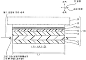
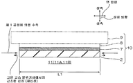
- B32B2307/704—Crystalline
Landscapes
- Chemical & Material Sciences (AREA)
- Engineering & Computer Science (AREA)
- Ceramic Engineering (AREA)
- Physics & Mathematics (AREA)
- Thermal Sciences (AREA)
- Chemical Kinetics & Catalysis (AREA)
- Materials Engineering (AREA)
- Mechanical Engineering (AREA)
- Metallurgy (AREA)
- Organic Chemistry (AREA)
- Laminated Bodies (AREA)
- Non-Insulated Conductors (AREA)
Applications Claiming Priority (2)
| Application Number | Priority Date | Filing Date | Title |
|---|---|---|---|
| JPJP-P-2017-186764 | 2017-09-27 | ||
| JP2017186764A JP2019059170A (ja) | 2017-09-27 | 2017-09-27 | 結晶化フィルム |
Publications (1)
| Publication Number | Publication Date |
|---|---|
| KR20190036475A true KR20190036475A (ko) | 2019-04-04 |
Family
ID=65864699
Family Applications (1)
| Application Number | Title | Priority Date | Filing Date |
|---|---|---|---|
| KR1020180109321A Withdrawn KR20190036475A (ko) | 2017-09-27 | 2018-09-13 | 결정화 필름 |
Country Status (4)
| Country | Link |
|---|---|
| JP (1) | JP2019059170A (https=) |
| KR (1) | KR20190036475A (https=) |
| CN (1) | CN109559842A (https=) |
| TW (1) | TW201916064A (https=) |
Families Citing this family (3)
| Publication number | Priority date | Publication date | Assignee | Title |
|---|---|---|---|---|
| WO2021187577A1 (ja) * | 2020-03-19 | 2021-09-23 | 日東電工株式会社 | 透明導電性フィルム |
| CN115298760A (zh) | 2020-03-19 | 2022-11-04 | 日东电工株式会社 | 透光性导电膜和透明导电性薄膜 |
| JP7659380B2 (ja) * | 2020-10-30 | 2025-04-09 | 日東電工株式会社 | 積層フィルムおよび歪みセンサの製造方法 |
Family Cites Families (8)
| Publication number | Priority date | Publication date | Assignee | Title |
|---|---|---|---|---|
| JP2002150842A (ja) * | 2000-11-15 | 2002-05-24 | Kanegafuchi Chem Ind Co Ltd | 透明導電膜付き高分子フィルム |
| JP4882262B2 (ja) * | 2005-03-31 | 2012-02-22 | 凸版印刷株式会社 | 透明導電膜積層体の製造方法 |
| CN102985585B (zh) * | 2010-07-06 | 2015-09-30 | 日东电工株式会社 | 透明导电性薄膜及其制造方法 |
| JP6031559B2 (ja) * | 2010-12-27 | 2016-11-24 | 日東電工株式会社 | 透明導電性フィルムおよびその製造方法 |
| JP5196001B2 (ja) * | 2011-09-29 | 2013-05-15 | 東洋紡株式会社 | 透明導電性フィルム及びその製造方法 |
| EP2942700B1 (en) * | 2013-11-27 | 2021-06-09 | LG Chem, Ltd. | Manufacturing method for conductive structure |
| JP2015146244A (ja) * | 2014-02-03 | 2015-08-13 | 凸版印刷株式会社 | 透明導電性フィルムおよびこの製造方法 |
| WO2015178298A1 (ja) * | 2014-05-20 | 2015-11-26 | 日東電工株式会社 | 透明導電性フィルムおよびその製造方法 |
-
2017
- 2017-09-27 JP JP2017186764A patent/JP2019059170A/ja active Pending
-
2018
- 2018-09-13 KR KR1020180109321A patent/KR20190036475A/ko not_active Withdrawn
- 2018-09-25 TW TW107133583A patent/TW201916064A/zh unknown
- 2018-09-26 CN CN201811125171.1A patent/CN109559842A/zh active Pending
Also Published As
| Publication number | Publication date |
|---|---|
| JP2019059170A (ja) | 2019-04-18 |
| CN109559842A (zh) | 2019-04-02 |
| TW201916064A (zh) | 2019-04-16 |
Similar Documents
| Publication | Publication Date | Title |
|---|---|---|
| KR101991545B1 (ko) | 투명 도전성 필름 및 그 제조 방법 | |
| JP6523357B2 (ja) | 透明導電性フィルムおよびその製造方法 | |
| JP7278372B2 (ja) | 透明導電性フィルム | |
| WO2012086484A1 (ja) | 透明導電性フィルムおよびその製造方法 | |
| US20130149555A1 (en) | Transparent conductive film and manufacturing method therefor | |
| JP6181806B2 (ja) | 透明導電性フィルムおよびその製造方法 | |
| JP6650770B2 (ja) | 導電性積層フィルム | |
| KR20190036475A (ko) | 결정화 필름 | |
| JP2009073090A (ja) | 機能性フィルム、機能性フィルムの製造方法、積層体、電子デバイス | |
| CN110197739B (zh) | 透明导电性薄膜层叠体及透明导电性薄膜的制造方法 | |
| JP2015191347A (ja) | 透明導電性フィルム積層体およびタッチパネルの製造方法 | |
| JP2020108941A (ja) | 透明導電性フィルム積層体 | |
| JP2005018551A (ja) | 電磁波シールド機能を有するタッチパネル、およびそれに用いる透明積層フィルム | |
| JP7270334B2 (ja) | 透明導電性フィルムおよびその製造方法 | |
| CN108602316A (zh) | 层叠薄膜 | |
| JP7492916B2 (ja) | 透明導電性フィルム | |
| JP7509690B2 (ja) | 結晶化インジウムスズ複合酸化物膜、透明導電性フィルムおよびその製造方法 | |
| WO2023063128A1 (ja) | 位相差層付偏光板およびそれを用いた画像表示装置 |
Legal Events
| Date | Code | Title | Description |
|---|---|---|---|
| PA0109 | Patent application |
Patent event code: PA01091R01D Comment text: Patent Application Patent event date: 20180913 |
|
| PG1501 | Laying open of application | ||
| PC1203 | Withdrawal of no request for examination | ||
| WITN | Application deemed withdrawn, e.g. because no request for examination was filed or no examination fee was paid |