KR20190036475A - Crystallization film - Google Patents
Crystallization film Download PDFInfo
- Publication number
- KR20190036475A KR20190036475A KR1020180109321A KR20180109321A KR20190036475A KR 20190036475 A KR20190036475 A KR 20190036475A KR 1020180109321 A KR1020180109321 A KR 1020180109321A KR 20180109321 A KR20180109321 A KR 20180109321A KR 20190036475 A KR20190036475 A KR 20190036475A
- Authority
- KR
- South Korea
- Prior art keywords
- film
- crystallized
- indium tin
- oxide layer
- composite oxide
- Prior art date
Links
Images


Classifications
-
- H—ELECTRICITY
- H01—ELECTRIC ELEMENTS
- H01B—CABLES; CONDUCTORS; INSULATORS; SELECTION OF MATERIALS FOR THEIR CONDUCTIVE, INSULATING OR DIELECTRIC PROPERTIES
- H01B5/00—Non-insulated conductors or conductive bodies characterised by their form
- H01B5/14—Non-insulated conductors or conductive bodies characterised by their form comprising conductive layers or films on insulating-supports
-
- B—PERFORMING OPERATIONS; TRANSPORTING
- B32—LAYERED PRODUCTS
- B32B—LAYERED PRODUCTS, i.e. PRODUCTS BUILT-UP OF STRATA OF FLAT OR NON-FLAT, e.g. CELLULAR OR HONEYCOMB, FORM
- B32B9/00—Layered products comprising a layer of a particular substance not covered by groups B32B11/00 - B32B29/00
- B32B9/005—Layered products comprising a layer of a particular substance not covered by groups B32B11/00 - B32B29/00 comprising one layer of ceramic material, e.g. porcelain, ceramic tile
-
- B—PERFORMING OPERATIONS; TRANSPORTING
- B32—LAYERED PRODUCTS
- B32B—LAYERED PRODUCTS, i.e. PRODUCTS BUILT-UP OF STRATA OF FLAT OR NON-FLAT, e.g. CELLULAR OR HONEYCOMB, FORM
- B32B27/00—Layered products comprising a layer of synthetic resin
- B32B27/06—Layered products comprising a layer of synthetic resin as the main or only constituent of a layer, which is next to another layer of the same or of a different material
- B32B27/08—Layered products comprising a layer of synthetic resin as the main or only constituent of a layer, which is next to another layer of the same or of a different material of synthetic resin
-
- B—PERFORMING OPERATIONS; TRANSPORTING
- B32—LAYERED PRODUCTS
- B32B—LAYERED PRODUCTS, i.e. PRODUCTS BUILT-UP OF STRATA OF FLAT OR NON-FLAT, e.g. CELLULAR OR HONEYCOMB, FORM
- B32B27/00—Layered products comprising a layer of synthetic resin
- B32B27/18—Layered products comprising a layer of synthetic resin characterised by the use of special additives
-
- B—PERFORMING OPERATIONS; TRANSPORTING
- B32—LAYERED PRODUCTS
- B32B—LAYERED PRODUCTS, i.e. PRODUCTS BUILT-UP OF STRATA OF FLAT OR NON-FLAT, e.g. CELLULAR OR HONEYCOMB, FORM
- B32B27/00—Layered products comprising a layer of synthetic resin
- B32B27/30—Layered products comprising a layer of synthetic resin comprising vinyl (co)polymers; comprising acrylic (co)polymers
- B32B27/308—Layered products comprising a layer of synthetic resin comprising vinyl (co)polymers; comprising acrylic (co)polymers comprising acrylic (co)polymers
-
- B—PERFORMING OPERATIONS; TRANSPORTING
- B32—LAYERED PRODUCTS
- B32B—LAYERED PRODUCTS, i.e. PRODUCTS BUILT-UP OF STRATA OF FLAT OR NON-FLAT, e.g. CELLULAR OR HONEYCOMB, FORM
- B32B27/00—Layered products comprising a layer of synthetic resin
- B32B27/32—Layered products comprising a layer of synthetic resin comprising polyolefins
- B32B27/325—Layered products comprising a layer of synthetic resin comprising polyolefins comprising polycycloolefins
-
- B—PERFORMING OPERATIONS; TRANSPORTING
- B32—LAYERED PRODUCTS
- B32B—LAYERED PRODUCTS, i.e. PRODUCTS BUILT-UP OF STRATA OF FLAT OR NON-FLAT, e.g. CELLULAR OR HONEYCOMB, FORM
- B32B27/00—Layered products comprising a layer of synthetic resin
- B32B27/40—Layered products comprising a layer of synthetic resin comprising polyurethanes
-
- B—PERFORMING OPERATIONS; TRANSPORTING
- B32—LAYERED PRODUCTS
- B32B—LAYERED PRODUCTS, i.e. PRODUCTS BUILT-UP OF STRATA OF FLAT OR NON-FLAT, e.g. CELLULAR OR HONEYCOMB, FORM
- B32B9/00—Layered products comprising a layer of a particular substance not covered by groups B32B11/00 - B32B29/00
- B32B9/04—Layered products comprising a layer of a particular substance not covered by groups B32B11/00 - B32B29/00 comprising such particular substance as the main or only constituent of a layer, which is next to another layer of the same or of a different material
- B32B9/045—Layered products comprising a layer of a particular substance not covered by groups B32B11/00 - B32B29/00 comprising such particular substance as the main or only constituent of a layer, which is next to another layer of the same or of a different material of synthetic resin
-
- C—CHEMISTRY; METALLURGY
- C23—COATING METALLIC MATERIAL; COATING MATERIAL WITH METALLIC MATERIAL; CHEMICAL SURFACE TREATMENT; DIFFUSION TREATMENT OF METALLIC MATERIAL; COATING BY VACUUM EVAPORATION, BY SPUTTERING, BY ION IMPLANTATION OR BY CHEMICAL VAPOUR DEPOSITION, IN GENERAL; INHIBITING CORROSION OF METALLIC MATERIAL OR INCRUSTATION IN GENERAL
- C23C—COATING METALLIC MATERIAL; COATING MATERIAL WITH METALLIC MATERIAL; SURFACE TREATMENT OF METALLIC MATERIAL BY DIFFUSION INTO THE SURFACE, BY CHEMICAL CONVERSION OR SUBSTITUTION; COATING BY VACUUM EVAPORATION, BY SPUTTERING, BY ION IMPLANTATION OR BY CHEMICAL VAPOUR DEPOSITION, IN GENERAL
- C23C14/00—Coating by vacuum evaporation, by sputtering or by ion implantation of the coating forming material
- C23C14/58—After-treatment
- C23C14/5806—Thermal treatment
-
- B—PERFORMING OPERATIONS; TRANSPORTING
- B32—LAYERED PRODUCTS
- B32B—LAYERED PRODUCTS, i.e. PRODUCTS BUILT-UP OF STRATA OF FLAT OR NON-FLAT, e.g. CELLULAR OR HONEYCOMB, FORM
- B32B2264/00—Composition or properties of particles which form a particulate layer or are present as additives
- B32B2264/02—Synthetic macromolecular particles
- B32B2264/0214—Particles made of materials belonging to B32B27/00
- B32B2264/0228—Vinyl resin particles, e.g. polyvinyl acetate, polyvinyl alcohol polymers or ethylene-vinyl acetate copolymers
- B32B2264/0235—Aromatic vinyl resin, e.g. styrenic (co)polymers
-
- B—PERFORMING OPERATIONS; TRANSPORTING
- B32—LAYERED PRODUCTS
- B32B—LAYERED PRODUCTS, i.e. PRODUCTS BUILT-UP OF STRATA OF FLAT OR NON-FLAT, e.g. CELLULAR OR HONEYCOMB, FORM
- B32B2264/00—Composition or properties of particles which form a particulate layer or are present as additives
- B32B2264/10—Inorganic particles
- B32B2264/102—Oxide or hydroxide
-
- B—PERFORMING OPERATIONS; TRANSPORTING
- B32—LAYERED PRODUCTS
- B32B—LAYERED PRODUCTS, i.e. PRODUCTS BUILT-UP OF STRATA OF FLAT OR NON-FLAT, e.g. CELLULAR OR HONEYCOMB, FORM
- B32B2270/00—Resin or rubber layer containing a blend of at least two different polymers
-
- B—PERFORMING OPERATIONS; TRANSPORTING
- B32—LAYERED PRODUCTS
- B32B—LAYERED PRODUCTS, i.e. PRODUCTS BUILT-UP OF STRATA OF FLAT OR NON-FLAT, e.g. CELLULAR OR HONEYCOMB, FORM
- B32B2307/00—Properties of the layers or laminate
- B32B2307/70—Other properties
- B32B2307/704—Crystalline
Landscapes
- Chemical & Material Sciences (AREA)
- Engineering & Computer Science (AREA)
- Ceramic Engineering (AREA)
- Physics & Mathematics (AREA)
- Thermal Sciences (AREA)
- Chemical Kinetics & Catalysis (AREA)
- Materials Engineering (AREA)
- Mechanical Engineering (AREA)
- Metallurgy (AREA)
- Organic Chemistry (AREA)
- Laminated Bodies (AREA)
- Non-Insulated Conductors (AREA)
Abstract
Description
본 발명은 결정화 필름에 관한 것이다.The present invention relates to a crystallized film.
종래, 투명 도전성 필름은, 결정화에 의해 저항값이 저감된 투명 도전층을 구비하고 있어, 터치 패널에 구비되는 것으로 알려져 있다.Conventionally, a transparent conductive film has a transparent conductive layer whose resistance value is reduced by crystallization, and is known to be provided in a touch panel.
예를 들어, 종래, 가요성 투명 기재, 및 그 위에 형성되고 결정화된 인듐·주석 복합 산화물 (결정성 ITO 막) 로 이루어지는 투명 도전층을 구비하고, 투명 도전층의 압축 잔류 응력이 0.4 ∼ 2 GPa 인 투명 도전성 필름이 제안되어 있다 (예를 들어, 일본 공개특허공보 2016-179686호 참조.).For example, conventionally, a transparent conductive layer made of a flexible transparent substrate and an indium-tin composite oxide (crystalline ITO film) formed and crystallized thereon is provided, and the transparent conductive layer has a compressive residual stress of 0.4 to 2 GPa (See, for example, JP-A-2016-179686).
일본 공개특허공보 2016-179686호에 기재된 투명 도전성 필름에서는, 압축 잔류 응력을 상기한 하한 이상으로 함으로써, 투명 도전성 필름을 게임기의 터치 패널에 사용할 때 중하중에서의 타점 특성 및 내굴곡성을 향상시켰다.In the transparent conductive film described in Japanese Laid-Open Patent Publication No. 2016-179686, the compression residual stress is set to the above-mentioned lower limit or higher, so that the rubbing property and flex resistance of the transparent conductive film are improved in medium and low loads when the transparent conductive film is used in a touch panel of a game machine.
그런데, 터치 패널이 예를 들어 차재되는 경우에는, 투명 도전성 필름은, 고온 고습 분위기에 노출된다. 그러나, 일본 공개특허공보 2016-179686호에 기재된 투명 도전성 필름은, 고온 고습 분위기에 노출되면, 투명 도전층에 크랙 (균열) 을 비교적 단시간에 발생시킨다는 문제가 있다.However, when the touch panel is mounted for example, the transparent conductive film is exposed to a high temperature and high humidity atmosphere. However, the transparent conductive film described in JP-A-2016-179686 has a problem in that cracks (cracks) are generated in the transparent conductive layer in a relatively short period of time when exposed to a high temperature and high humidity atmosphere.
본 발명은, 고온 고습 분위기에 노출되어도, 비교적 단시간에서는 손상을 발생시키는 것을 억제할 수 있는 결정화 필름을 제공하는 것에 있다.An object of the present invention is to provide a crystallized film capable of suppressing occurrence of damage in a relatively short time even when exposed to a high temperature and high humidity atmosphere.
본 발명 (1) 은, 투명 필름 기재 및 결정화 인듐 주석 복합 산화물층을 구비하는 결정화 필름으로서, 상기 결정화 필름은, 투명 필름 기재 및 비정질 인듐 주석 복합 산화물층을 구비하는 비정질 필름을 특정 온도에서 결정화시킴으로써 얻어지는 특정 온도 결정화 필름으로서, 상기 특정 온도 결정화 필름에 있어서의 결정화 인듐 주석 복합 산화물층의 잔류 응력 σ1 과, 상기 비정질 필름을 110 ℃ 에서 결정화시킴으로써 얻어지는 110 ℃ 결정화 필름에 있어서의 결정화 인듐 주석 복합 산화물층의 잔류 응력 σ2 의 차이가, 150 MPa 이하인, 결정화 필름을 포함한다.The present invention (1) is a crystallization film comprising a transparent film base and a crystallized indium tin composite oxide layer, wherein the crystallization film is obtained by crystallizing an amorphous film comprising a transparent film base and an amorphous indium tin composite oxide layer at a specific temperature The residual stress σ1 of the indium tin oxide complex oxide layer in the specific temperature-crystallized film and the residual stress σ1 of the amorphous indium tin compound oxide layer in the 110 캜 crystallized film obtained by crystallizing the amorphous film at 110 캜 Of the residual stress? 2 is 150 MPa or less.
본 발명 (2) 는, 상기 특정 온도 결정화 필름은, 상기 비정질 필름의 상기 특정 온도에서의 가열에 의해 상기 비정질 필름에 대하여 수축되어 있고, 상기 110 ℃ 결정화 필름은, 상기 비정질 필름의 110 ℃ 에서의 가열에 의해 상기 비정질 필름에 대하여 수축되어 있고, 상기 특정 온도 결정화 필름의 수축률 SR1 과 상기 110 ℃ 결정화 필름의 수축률 SR2 의 차이가, 0.05 % 이하인, (1) 에 기재된 결정화 필름을 포함한다.In the present invention (2), the amorphous film is shrunk to the amorphous film by heating at the specific temperature, and the 110 ° C crystallized film is a film of the amorphous film at 110 ° C And the crystallization film according to (1), wherein the amorphous film is shrunk by heating, and the difference between the shrinkage ratio SR1 of the specific temperature-crystallized film and the shrinkage ratio SR2 of the 110 占 폚 crystallized film is 0.05% or less.
본 발명 (3) 은, 상기 특정 온도 결정화 필름 및 상기 110 ℃ 결정화 필름은 모두 일정한 인장 하중하에서, 25 ℃ 및 10 % RH 로부터 85 ℃ 및 85 % RH 로 가열 및 가습될 때에 신장되고, 상기 특정 온도 결정화 필름의 신장률 EP1 과 상기 110 ℃ 결정화 필름의 신장률 EP2 의 차이가, 0.07 % 이하인, (1) 또는 (2) 에 기재된 결정화 필름을 포함한다.The present invention (3) is characterized in that the specific temperature-crystallized film and the 110 ° C crystallized film both elongate when heated and humidified at 25 ° C and 10% RH at 85 ° C and 85% RH under a constant tensile load, (1) or (2) wherein the difference between the elongation percentage EP1 of the crystallization film and the elongation percentage EP2 of the 110 占 폚 crystallization film is 0.07% or less.
본 발명의 특정 온도 결정화 필름에 있어서의 결정화 인듐 주석 복합 산화물층의 잔류 응력 σ1 과, 비정질 필름을 110 ℃ 에서 결정화시킴으로써 얻어지는 110 ℃ 결정화 필름에 있어서의 결정화 인듐 주석 복합 산화물층의 잔류 응력 σ2 의 차이는, 150 MPa 이하로 작다.The residual stress σ1 of the indium tin oxide complex oxide layer in the specific temperature-crystallized film of the present invention and the difference in residual stress σ2 of the indium tin oxide complex oxide layer in the 110 캜 crystallized film obtained by crystallizing the amorphous film at 110 캜 Is as small as 150 MPa or less.
그래서, 본 발명의 특정 온도 결정화 필름을 고온 고습 분위기에 노출시켜도, 비교적 단시간에서는 손상을 발생시키는 것을 억제할 수 있다.Therefore, even when the specific temperature-crystallized film of the present invention is exposed to a high-temperature and high-humidity atmosphere, it is possible to suppress the occurrence of damage in a relatively short time.
도 1A 및 도 1B 는, 본 발명의 결정화 필름의 일 실시형태의 제조 방법을 나타내는 공정 단면도로서, 도 1A 가 비정질 필름을 제조하는 제 1 공정, 도 1B 가 결정화 필름을 제조하는 제 2 공정을 나타낸다.
도 2A 및 도 2B 는, 도 1A 및 도 1B 에 나타내는 결정화 필름의 변형예 (비정질 인듐 주석 복합 산화물층 및 투명 필름 기재로만 이루어지는 결정화 필름) 의 제조 방법의 공정 단면도로서, 도 2A 가 비정질 필름을 제조하는 제 1 공정, 도 2B 가 결정화 필름을 제조하는 제 2 공정을 나타낸다.
도 3 은, 실시예에 있어서, 잔류 응력의 산출에 사용되는 X 선 산란법에 있어서의 각도 θ 및 Ψ 를 설명하기 위한 개략도이다.1A and 1B are process sectional views showing a manufacturing method of an embodiment of the crystallization film of the present invention, in which FIG. 1A shows a first process for producing an amorphous film and FIG. 1B shows a second process for producing a crystallized film .
2A and 2B are process sectional views of a modification of the crystallized film shown in Figs. 1A and 1B (a crystalline film comprising only an amorphous indium tin composite oxide layer and a transparent film base) And Fig. 2B shows a second step of producing a crystallized film.
Fig. 3 is a schematic view for explaining the angles? And? In the X-ray scattering method used in the calculation of the residual stress in the embodiment. Fig.
<일 실시형태> <Embodiment>
본 발명의 결정화 필름의 일 실시형태를, 도 1A 및 도 1B 를 참조하여 설명한다.One embodiment of the crystallization film of the present invention will be described with reference to Figs. 1A and 1B.
도 1A 및 도 1B 에 있어서, 지면 상하 방향은 상하 방향 (두께 방향, 제 1 방향) 으로, 지면 상측이 상측 (두께 방향 일방측, 제 1 방향 일방측), 지면 하측이 하측 (두께 방향 타방측, 제 1 방향 타방측) 이다. 또한, 지면 좌우 방향 및 안쪽 길이 방향은, 상하 방향과 직교하는 면 방향이다. 구체적으로는, 각 도면의 방향 화살표에 준거한다.1A and 1B, the upper side of the drawing is defined as the upper side (one side in the thickness direction, one side in the first direction), the lower side of the sheet is the lower side (the other side in the thickness direction , The other side in the first direction). The left-right direction and the inner-length direction on the paper surface are plane directions perpendicular to the up-down direction. Specifically, it is based on the directional arrows in each drawing.
(결정화 필름)(Crystallization film)
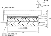
도 1B 에 나타내는 바와 같이, 결정화 필름 (11) 은, 소정 두께를 갖는 필름 형상 (시트 형상을 포함한다) 을 이루며, 면 방향으로 신장되고, 평탄한 상면 및 평탄한 하면을 갖는다. 결정화 필름 (11) 은, 예를 들어 화상 표시 장치에 유리층 (9) 및 감압 접착제층 (8) (후술) 과 함께 구비되는 터치 패널용 기재 등을 제작하기 위한 한 부품으로, 요컨대 화상 표시 장치는 아니다. 즉, 결정화 필름 (11) 은, LCD 모듈 등의 화상 표시 소자, 유리층 (9), 감압 접착제층 (8) 등을 포함하지 않고, 부품 단독으로 유통되어 산업상 이용 가능한 디바이스이다.As shown in Fig. 1B, the
결정화 필름 (11) 은, 예를 들어 안티 블로킹층 (4), 투명 필름 기재 (2), 하드 코트층 (3), 광학 조정층 (5) 및 결정화 인듐 주석 복합 산화물층 (7) 을 상측을 향해 차례로 구비한다. 바람직하게는 결정화 필름 (11) 은, 안티 블로킹층 (4), 투명 필름 기재 (2), 하드 코트층 (3), 광학 조정층 (5) 및 결정화 인듐 주석 복합 산화물층 (7) 으로만 이루어진다. 이하, 각 층을 순서대로 설명한다.The
(투명 필름 기재)(Transparent film base)
투명 필름 기재 (2) 는, 결정화 필름 (11) 의 기계 강도를 확보하기 위한 투명한 기재이다. 구체적으로는 투명 필름 기재 (2) 는, 결정화 인듐 주석 복합 산화물층 (7) 을, 하드 코트층 (3) 및 광학 조정층 (5) 과 함께 지지하고 있다.The transparent
또, 투명 필름 기재 (2) 는, 이후에 상세히 서술하겠지만, 도 1B 의 화살표로 나타내는 바와 같은 면 방향 내측으로의 수축력을 갖고 있고, 이 수축력에 의해 결정화 인듐 주석 복합 산화물층 (7) 에 잔류 응력 σ1 을 부여한다.The transparent
투명 필름 기재 (2) 는, 필름 형상을 갖고 있으며, 면 방향으로 신장되고, 평탄한 상면 및 평탄한 하면을 갖는다.The transparent
투명 필름 기재 (2) 는, 예를 들어 가요성을 갖는 투명 필름이다. 투명 필름 기재 (2) 의 재료로서는, 특별히 한정되지 않고, 예를 들어 시클로올레핀계 수지, 폴리에스테르계 수지 (폴리에틸렌테레프탈레이트 (PET) 등), 아세테이트계 수지, 폴리에테르술폰계 수지, 폴리카보네이트계 수지, 폴리아미드계 수지, 폴리이미드계 수지, 올레핀계 수지, (메트)아크릴계 수지, 폴리염화비닐계 수지, 폴리염화비닐리덴계 수지, 폴리스티렌계 수지, 폴리비닐알코올계 수지, 폴리아릴레이트계 수지, 폴리페닐렌술파이드계 수지 등을 들 수 있다.The transparent
투명 필름 기재 (2) 의 재료로서, 바람직하게는 시클로올레핀계 수지를 들 수 있다. 투명 필름 기재 (2) 의 재료가 시클로올레핀계 수지이면, 투명 필름 기재 (2) 를 등방성 투명 필름으로 할 수 있고, 결정화 필름 (11) 에 등방성을 부여할 수 있다.As a material of the transparent
투명 필름 기재 (2) 는, 등방성 또는 복굴절성을 갖는다. 투명 필름 기재 (2) 는, 바람직하게는 등방성을 갖는다. 투명 필름 기재 (2) 의 면내 방향의 복굴절률은, 예를 들어 200 이하, 바람직하게는 150 이하이며, 또한, 예를 들어 0 이상이다.The transparent
투명 필름 기재 (2) 의 두께는, 예를 들어 100 ㎛ 이하, 바람직하게는 50 ㎛ 이하이며, 또한, 예를 들어 5 ㎛ 이상, 바람직하게는 15 ㎛ 이상이다.The thickness of the
(하드 코트층) (Hard coat layer)
하드 코트층 (3) 은, 결정화 필름 (11) (또는 후술하는 제조 도중의 비정질 필름 (1)) 에 찰상을 잘 발생시키지 않게 하기 위한 찰상 보호층이다. 하드 코트층 (3) 은, 필름 형상을 갖고 있고, 예를 들어 투명 필름 기재 (2) 의 상면 전체면에, 투명 필름 기재 (2) 의 상면에 접촉하도록 배치되어 있다. 하드 코트층 (3) 의 재료는, 예를 들어 하드 코트 조성물이다. 하드 코트 조성물로는, 예를 들어 일본 공개특허공보 2016-179686호에 기재된 혼합물 등을 들 수 있다. 혼합물은, 예를 들어 아크릴계 수지, 우레탄계 수지 등의 수지 (바인더 수지) 를 함유한다. 하드 코트층 (3) 의 두께는, 예를 들어 0.1 ㎛ 이상, 바람직하게는 0.5 ㎛ 이상이며, 또한, 예를 들어 10 ㎛ 이하, 바람직하게는 5 ㎛ 이하이다.The
(광학 조정층) (Optical adjustment layer)
광학 조정층 (5) 은, 결정화 인듐 주석 복합 산화물층 (7) 에 있어서의 투명 전극 패턴의 시인 (視認) 을 억제하면서, 결정화 필름 (11) 에 우수한 투명성을 확보하기 위해서, 결정화 필름 (11) 의 광학 물성 (예를 들어, 굴절률) 을 조정하는 층이다.The optical adjustment layer 5 is formed by the
광학 조정층 (5) 은, 필름 형상을 갖고 있고, 예를 들어 하드 코트층 (3) 의 상면 전체면에, 하드 코트층 (3) 의 상면에 접촉하도록 배치되어 있다. 보다 구체적으로는 광학 조정층 (5) 은, 하드 코트층 (3) 과 결정화 인듐 주석 복합 산화물층 (7) 의 사이에, 하드 코트층 (3) 의 상면 및 결정화 인듐 주석 복합 산화물층 (7) 의 하면에 접촉하도록 배치되어 있다. 광학 조정층 (5) 의 재료는, 예를 들어 광학 조정 조성물이다. 광학 조정 조성물로는, 예를 들어 일본 공개특허공보 2016-179686호에 기재된 혼합물 등을 들 수 있다. 혼합물은, 예를 들어 아크릴계 수지 등의 수지 (바인더 수지) 와, 무기계 또는 유기계 입자 (바람직하게는 지르코니아 등의 무기계 입자) 를 함유한다. 광학 조정층 (5) 의 두께는, 예를 들어 50 nm 이상, 바람직하게는 100 nm 이상이며, 또한, 예를 들어 800 nm 이하, 바람직하게는 300 nm 이하이다.The optical adjustment layer 5 has a film shape and is disposed, for example, on the entire upper surface of the
(안티 블로킹층) (Anti-blocking layer)
안티 블로킹층 (4) 은, 복수의 결정화 필름 (11) (제조 도중의 비정질 필름 (1)) 을 두께 방향으로 적층한 경우 등에, 서로 접촉하는 복수의 결정화 필름 (11) 의 표면에 내블로킹성을 부여한다. 안티 블로킹층 (4) 은, 결정화 필름 (11) 에 있어서의 최하면을 이룬다. 구체적으로는 안티 블로킹층 (4) 은, 투명 필름 기재 (2) 의 하면 전체면에, 투명 필름 기재 (2) 의 하면에 접촉하도록 배치되어 있다.The
안티 블로킹층 (4) 의 재료는, 예를 들어 안티 블로킹 조성물이다. 안티 블로킹 조성물로는, 예를 들어 일본 공개특허공보 2016-179686호에 기재된 혼합물 등을 들 수 있다. 혼합물은, 예를 들어 아크릴계 수지 등의 수지 (바인더 수지) 와, 무기계 또는 유기계 입자 (바람직하게는 스티렌계 등의 유기계 입자) 를 함유한다. 안티 블로킹층 (4) 의 두께는, 예를 들어 0.1 ㎛ 이상, 바람직하게는 0.5 ㎛ 이상이며, 또한, 예를 들어 10 ㎛ 이하, 바람직하게는 5 ㎛ 이하이다.The material of the
(결정화 인듐 주석 복합 산화물층) (Crystallized indium tin complex oxide layer)
결정화 인듐 주석 복합 산화물층 (7) 은, 에칭 등의 후공정에서 투명 전극 패턴에 형성하기 위한 투명 도전층이다. 또, 후술하겠지만, 결정화 인듐 주석 복합 산화물층 (7) 은, 비정질 인듐 주석 복합 산화물층 (6) (도 1A 참조) 을 특정 온도에서 결정화시킨 결정화층 (특정 온도 결정화층) 이다. 결정화 인듐 주석 복합 산화물층 (7) 은, 결정질이므로, 비교적 딱딱하다. 결정화 인듐 주석 복합 산화물층 (7) 은, 광학 조정층 (5) 및 하드 코트층 (3) 을 개재하여 투명 필름 기재 (2) 에 지지되고 있다.The crystallized indium tin
결정화 인듐 주석 복합 산화물층 (7) 은, 결정화 필름 (11) 의 최상층으로서, 필름 형상을 갖고 있으며, 광학 조정층 (5) 의 상면 전체면에, 광학 조정층 (5) 의 상면에 접촉하도록 배치되어 있다.The crystallized indium tin
또, 결정화 인듐 주석 복합 산화물층 (7) 은, 이후에 상세히 서술하겠지만, 도 1B 의 화살표로 나타내는 바와 같은 투명 필름 기재 (2) 의 수축력에 기초하여 잔류 응력 σ1 을 갖는다.The crystallized indium tin
결정화 인듐 주석 복합 산화물층 (7) 의 재료는, 결정질 인듐 주석 복합 산화물 (ITO) 이다. ITO 는, 인듐 (In) 과 주석 (Sn) 을 필수 성분으로서 함유하는 복합 산화물이다. 구체적으로는 ITO 는, 산화주석 (SnO2) 및 산화인듐 (In2O3) 을 주성분으로서 함유한다. 산화주석의 함유 비율은, 산화주석 및 산화인듐의 합계량에 대하여 예를 들어 0.5 질량% 이상, 바람직하게는 3 질량% 이상이며, 또한, 예를 들어 15 질량% 이하, 바람직하게는 13 질량% 이하이다. 산화인듐의 함유 비율은, 상기한 합계량에 있어서의 산화주석의 함유 비율의 잔부이다. 또, ITO 는, 주성분 (필수 성분) 이외의 추가 성분, 구체적으로는 Zn, Ga, Sb, Ti, Si, Zr, Mg, Al, Au, Ag, Cu, Pd, W, Fe, Pb, Ni, Nb, Cr, Ga 등의 추가 성분을 함유할 수도 있다.The material of the crystallized indium tin
결정화 인듐 주석 복합 산화물층 (7) 의 두께는, 예를 들어 10 nm 이상, 바람직하게는 20 nm 이상이며, 또한, 예를 들어 100 nm 이하, 바람직하게는 35 nm 이하이다.The thickness of the crystallized indium tin
결정화 인듐 주석 복합 산화물층 (7) 의 표면 저항은, 예를 들어 200 Ω/□ 이하, 바람직하게는 150 Ω/□ 이하이며, 또한, 예를 들어 10 Ω/□ 이상이다. 결정화 인듐 주석 복합 산화물층 (7) 의 표면 저항은, 사단자법에 의해 측정된다.The surface resistance of the crystallized indium tin
(결정화 투명 도전성 필름의 제조 방법) (Method for producing crystallized transparent conductive film)
다음으로, 결정화 필름 (11) 을 제조하는 방법을, 도 1A 및 도 1B 를 참조하여 설명한다.Next, a method of manufacturing the
이 방법에서는, 먼저, 도 1A 에 나타내는 바와 같이, 비정질 필름 (1) 을 제조하고 (제 1 공정), 그 후, 도 1B 에 나타내는 바와 같이, 비정질 필름 (1) 을 결정화시켜, 결정화 필름 (11) 을 제조한다 (제 2 공정).1A, first, an
(제 1 공정) (First step)
제 1 공정에서는, 비정질 필름 (1) 을 제조한다.In the first step, the amorphous film (1) is produced.
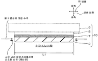
비정질 필름 (1) 은, 도 1A 에 나타내는 바와 같이, 비정질 필름 (1) 은, 안티 블로킹층 (4), 투명 필름 기재 (2), 하드 코트층 (3), 광학 조정층 (5) 및 비정질 인듐 주석 복합 산화물층 (6) 을 상측을 향해 차례로 구비한다. 바람직하게는 결정화 필름 (11) 은, 안티 블로킹층 (4), 투명 필름 기재 (2), 하드 코트층 (3), 광학 조정층 (5) 및 비정질 인듐 주석 복합 산화물층 (6) 으로만 이루어진다.1A, the
도 1A 에 나타내는 비정질 필름 (1) 에 있어서의 안티 블로킹층 (4), 투명 필름 기재 (2), 하드 코트층 (3) 및 광학 조정층 (5) 은, 도 1B 에 나타내는 그것들과 동일하다.The
비정질 인듐 주석 복합 산화물층 (6) 은, 결정화 인듐 주석 복합 산화물층 (7) 의 결정화 전의 비정질층이다. 비정질 인듐 주석 복합 산화물층 (6) 은, 비정질이므로, 비교적 부드럽다 (연하다). 비정질 인듐 주석 복합 산화물층 (6) 의 재료 및 두께는, 결정화 인듐 주석 복합 산화물층 (7) 에서 예시한 그것들과 동일하다. 비정질 인듐 주석 복합 산화물층 (6) 의 표면 저항값은, 예를 들어 200 Ω/□ 초과, 나아가서는 250 Ω/□ 이상, 더 나아가서는 300 Ω/□ 이상이며, 또한, 예를 들어 500 Ω/□ 이하이다. 비정질 인듐 주석 복합 산화물층 (6) 의 표면 저항은, 사단자법에 의해 측정된다.The amorphous indium tin
비정질 필름 (1) 의 제조 방법은, 특별히 한정되지 않고, 예를 들어 먼저, 투명 필름 기재 (2) 를 준비하고, 이어서, 투명 필름 기재 (2) 에 대하여 하드 코트층 (3), 안티 블로킹층 (4), 광학 조정층 (5) 및 비정질 인듐 주석 복합 산화물층 (6) 을 차례로 배치한다. 구체적으로는, 투명 필름 기재 (2) 의 상하 양면 각각에, 하드 코트 조성물의 희석액 및 안티 블로킹 조성물의 희석액을 도포하고, 건조 후, 자외선 조사에 의해 하드 코트 조성물 및 안티 블로킹 조성물의 각각을 경화시킨다. 이로써, 투명 필름 기재 (2) 의 상하 양면 각각에, 하드 코트층 (3) 및 안티 블로킹층 (4) 의 각각을 형성한다. 그 후, 광학 조정 조성물의 희석액을, 하드 코트층 (3) 의 상면에 도포하고, 건조 후, 자외선 조사에 의해 광학 조정 조성물을 경화시킨다. 이로써, 광학 조정층 (5) 을 형성한다.The method for producing the
그 후, 비정질 인듐 주석 복합 산화물층 (6) 을, 예를 들어 스퍼터링법 등으로 광학 조정층 (5) 의 상면에 형성한다. 또, 비정질 인듐 주석 복합 산화물층 (6) 은, 광학 조정층 (5) 및 하드 코트층 (3) 을 개재하여 투명 필름 기재 (2) 에 지지되고 있다. 또, 비정질 인듐 주석 복합 산화물층 (6) 은, 무부하에서 (상세하게는 면 방향에 있어서의 응력을 갖지 않음) 투명 필름 기재 (2) 에 지지되고 있다.Thereafter, the amorphous indium tin
또한, 각 층을, 예를 들어 롤 투 롤 방식으로 투명 필름 기재 (2) 에 대하여 형성할 수 있거나, 또는 이들 층의 일부 또는 전부를 배치 방식 (매엽 방식) 으로 형성할 수도 있다.Further, each layer may be formed on the
(제 2 공정)(Second Step)
제 2 공정에서는, 도 1B 에 나타내는 바와 같이, 비정질 필름 (1) 을 특정 온도에서 가열하여, 비정질 인듐 주석 복합 산화물층 (6) 을 결정화시킨다.In the second step, as shown in Fig. 1B, the
가열은, 예를 들어 적외선 히터, 오븐 등을 사용하여 실시할 수 있다.The heating can be performed using, for example, an infrared heater, an oven, or the like.
특정 온도, 요컨대, 가열 온도는, 예를 들어 110 ℃ 이상, 바람직하게는 110 ℃ 초과, 보다 바람직하게는 115 ℃ 이상, 더욱 바람직하게는 120 ℃ 이상, 특히 바람직하게는 125 ℃ 이상이며, 또한, 예를 들어 150 ℃ 미만, 바람직하게는 145 ℃ 이하, 보다 바람직하게는 140 ℃ 이하, 더욱 바람직하게는 135 ℃ 이하, 특히 바람직하게는 130 ℃ 이하이다. 가열 시간은, 가열 온도에 따라 적절히 결정되지만, 예를 들어 5 분 이상, 바람직하게는 10 분 이상, 보다 바람직하게는 15 분 이상, 더욱 바람직하게는 20 분 이상, 특히 바람직하게는 25 분 이상이며, 또한, 예를 들어 5 시간 이하, 바람직하게는 1 시간 이하, 바람직하게는 50 분 이하, 보다 바람직하게는 45 분 이하, 더욱 바람직하게는 40 분 이하이다.The heating temperature is, for example, at least 110 ° C, preferably at least 110 ° C, more preferably at least 115 ° C, more preferably at least 120 ° C, particularly preferably at least 125 ° C, For example, less than 150 ° C, preferably not more than 145 ° C, more preferably not more than 140 ° C, more preferably not more than 135 ° C, particularly preferably not more than 130 ° C. The heating time is appropriately determined depending on the heating temperature, but is, for example, 5 minutes or more, preferably 10 minutes or more, more preferably 15 minutes or more, further preferably 20 minutes or more, particularly preferably 25 minutes or more For example, 5 hours or less, preferably 1 hour or less, preferably 50 minutes or less, more preferably 45 minutes or less, further preferably 40 minutes or less.
가열이 상기 조건보다 가혹하면 (구체적으로는, 가열 온도가 상기 상한 온도를 초과하면, 및/또는 가열 시간이 상기 상한을 초과하면), 결정화 필름 (11) 이 고온 고습 분위기하에 노출되면, 비교적 단시간에서도 크랙 등의 손상을 발생시키는 것을 억제할 수 없는 경우가 있다.When the
한편, 가열이 상기 조건보다 온화 (완만) 하면 (구체적으로는, 가열 온도가 상기 하한 온도에 미치지 못하면, 및/또는 가열 시간이 상기 하한 온도에 미치지 못하면), 비정질 인듐 주석 복합 산화물층 (6) 을 확실히 결정화시켜, 결정화 인듐 주석 복합 산화물층 (7) 을 얻을 수 없는 경우가 있다. 특히, 가열 온도가 110 ℃ 에 미치지 못하면, 비정질 인듐 주석 복합 산화물층 (6) 을 확실히 결정화시켜, 결정화 인듐 주석 복합 산화물층 (7) 을 확실히 얻을 수 없는 경우가 있다. 바꿔 말하면, 제 2 공정에 있어서, 비정질 인듐 주석 복합 산화물층 (6) 을 결정화시켜 결정화 인듐 주석 복합 산화물층 (7) 을 제조하기 위한 최저 가열 온도는, 예를 들어 110 ℃ 이다.On the other hand, the amorphous indium tin
또한, 가열이 상기 조건의 범위 내이면, 이후에 상세히 서술하는 잔류 응력의 차이, 수축률의 차이, 신장률의 차이를 원하는 범위로 할 수 있다.Further, if the heating is within the above-mentioned range, the difference in residual stress, the difference in shrinkage percentage, and the difference in elongation percentage, which will be described in detail later, can be set in a desired range.
이로써, 도 1B 에 나타내는 바와 같이, 비정질 인듐 주석 복합 산화물층 (6) 이 결정화되어, 결정화 인듐 주석 복합 산화물층 (7) 이 된다. 그러면, 안티 블로킹층 (4), 투명 필름 기재 (2), 하드 코트층 (3), 광학 조정층 (5) 및 결정화 인듐 주석 복합 산화물층 (7) 을 상측을 향해 차례로 구비하는 결정화 필름 (11) 을 얻는다. 결정화 필름 (11) 은, 비정질 필름 (1) 을 특정 온도에서 가열한 특정 온도 결정화 필름 (11A) 이다. 특정 온도 결정화 필름 (11A) 에 있어서, 결정화 인듐 주석 복합 산화물층 (7) 은, 비정질 인듐 주석 복합 산화물층 (6) 을 특정 온도에서 결정화시킨 특정 온도 결정화층 (7A) 이다.Thereby, as shown in Fig. 1B, the amorphous indium tin
그 후, 예를 들어 방랭 등에 의해 결정화 필름 (11) 이 냉각된다. 냉각 온도는, 통상적으로 상온 (예를 들어, 20 ∼ 30 ℃, 구체적으로는 25 ℃ 정도 또는 실온) 이다.Thereafter, the crystallized
이와 같이 하여 제조된 결정화 필름 (11) 은, 다음에 설명하는 용도에 사용된다.The crystallized
(투명 도전성 필름의 용도) (Use of transparent conductive film)
결정화 필름 (11) 에 있어서, 결정화 인듐 주석 복합 산화물층 (7) 의 상면에, 도 1B 의 가상선으로 나타내는 유리층 (9) 을 감압 접착제층 (8) 을 통해서 접착시켜, 결정화 필름 (11) 의 상면을 보호할 수 있다. 결정화 인듐 주석 복합 산화물층 (7) 은, 결정화 필름 적층체 (10) 에 구비된다. 결정화 필름 적층체 (10) 는, 안티 블로킹층 (4), 투명 필름 기재 (2), 하드 코트층 (3), 광학 조정층 (5), 결정화 인듐 주석 복합 산화물층 (7), 감압 접착제층 (8) 및 유리층 (9) 을 상측을 향해 차례로 구비한다.The
결정화 필름 적층체 (10) 는, 예를 들어 화상 표시 장치에 구비된다.The crystallized
또한, 그러한 화상 표시 장치는, 예를 들어 차재 용도 등에 사용된다.Such an image display apparatus is used, for example, in a vehicle application.
(비정질 필름의 가열, 결정화 필름의 냉각, 및 결정화 필름의 가열 가습)(Heating of the amorphous film, cooling of the crystallized film, and heating and humidification of the crystallized film)
다음으로, 비정질 필름 (1) 의 가열 및 결정화 필름 (11) 의 냉각에서 기인되는 결정화 인듐 주석 복합 산화물층 (7) 의 잔류 응력 및 결정화 필름 (11) 의 수축과, 일정한 인장 하중하에 있어서 결정화 필름 (11) 이 가열 가습되었을 때의 신장에 대해서 상세히 설명한다.Next, the residual stress of the crystallized indium tin
[1] 제 1 공정 후, 제 2 공정 전의 비정질 필름[1] After the first step, the amorphous film before the second step
도 1A 에 나타내는 바와 같이, 제 1 공정에 의해 제조되는 비정질 필름 (1) 에 있어서, 비정질 인듐 주석 복합 산화물층 (6) 및 투명 필름 기재 (2) 는, 그것들이 노출되는 분위기가 통상적으로 상온이다. 그래서, 투명 필름 기재 (2) 및 비정질 인듐 주석 복합 산화물층 (6) 은, 서로 수축 및 신장 어느 것도 되지 않는다. 따라서, 비정질 인듐 주석 복합 산화물층 (6) 은, 잔류 응력을 갖지 않는다.1A, in the
또, 상온 분위기에 있어서의 수증기 농도는, 비교적 낮으며, 예를 들어 20 ℃ 에서 17 g/㎥, 25 ℃ 에서 23 g/㎥, 30 ℃ 에서 30 g/㎥ 이기 때문에, 수증기 농도의 범위는 17 g/㎥ ∼ 30 g/㎥ 정도이다. 그래서, 이와 같은 낮은 습도 (저습 또는 상습 (常濕)) 분위기에서는, 비정질 인듐 주석 복합 산화물층 (6) 및 투명 필름 기재 (2) 에 영향 (열화 등) 을 실질적으로 미치지 않는다.Since the concentration of water vapor in the room temperature atmosphere is relatively low, for example, 17 g /
[2] 제 2 공정에 있어서의 비정질 필름의 가열[2] Heating of the amorphous film in the second step
이어서, 제 2 공정에서는, 가열에 의해 투명 필름 기재 (2) 는, 도 1A 의 화살표에 나타내는 바와 같이 면 방향 외측을 향해 신장 (팽창) 된다.Subsequently, in the second step, the transparent
이와 동시에, 가열 도중에 있어서 비정질 인듐 주석 복합 산화물층 (6) 은, 비정질이므로, 비교적 부드럽기 (연하기) 때문에, 투명 필름 기재 (2) 의 신장에 수반되어, 도 1A 에 나타내는 바와 같이, 면 방향 외측을 향해 신장된다 (추종된다). 그래서, 제 2 공정의 가열에 의해, 비정질 인듐 주석 복합 산화물층 (6) 이 결정화된 결정화 인듐 주석 복합 산화물층 (7) 은, 잔류 응력을 갖지 않는다.At the same time, during the heating, the amorphous indium tin
[3] 제 2 공정에 있어서의 결정화 필름의 냉각[3] Cooling of the crystallized film in the second step
그 후, 결정화 필름 (11) 은, 상온으로 냉각된다. 그러면, 도 1B 의 실선 화살표로 나타내는 바와 같이, 투명 필름 기재 (2) 는, 면 방향 내측을 향해 크게 수축된다. 한편, 결정화 인듐 주석 복합 산화물층 (7) 은, 결정질이며, 비교적 (비정질 인듐 주석 복합 산화물층 (6) 에 비해서) 딱딱하기 때문에, 투명 필름 기재 (2) 에 완전하게는 추종되지 않는다. 구체적으로는 결정화 인듐 주석 복합 산화물층 (7) 은, 투명 필름 기재 (2) 의 수축에 비해서 작게 수축된다. 그래서, 결정화 인듐 주석 복합 산화물층 (7) 에는, 면 방향 내측을 향하는 잔류 응력 σ1 이 발생한다.Thereafter, the
냉각 후의 결정화 필름 (11) (투명 필름 기재 (2)) 의 치수 (구체적으로는, 도 1B 에 있어서의 길이 L1) 는, 가열 전의 비정질 필름 (1) (투명 필름 기재 (2)) 의 치수 (구체적으로는, 도 1A 에 있어서의 길이 L0) 에 비해서 작아진다. 요컨대, 비정질 필름 (1) 은, 비정질 필름 (1) 에 대하여 수축되어 있다. 결정화 필름 (11) 의 수축량 (L1-L0) 은, 비정질 필름 (1) 의 가열 온도 (특정 온도) 가 높아지면 증대되고, 비정질 필름 (1) 의 가열 온도 (특정 온도) 가 낮아지면 저감된다.The dimensions (specifically, the length L1 in Fig. 1B) of the crystallized film 11 (the transparent film substrate 2) after cooling is determined by the dimensions (the length L1 in Fig. 1B) of the
[4] 고온 고습 분위기하에 있어서의 결정화 필름[4] Crystallization film under high temperature and high humidity atmosphere
그 후, 제조된 결정화 필름 (11) 은, 상기한 차재 용도에 사용되는 경우에는, 고온 고습 분위기하에 노출된다. 온도 (고온) 는, 예를 들어 40 ℃ 이상, 나아가서는 50 ℃ 이상, 더 나아가서는 60 ℃ 이상, 특히 더 나아가서는 70 ℃ 이상인 한편, 또한, 예를 들어 110 ℃ (후술하는 최저 가열 온도) 미만, 나아가서는 105 ℃ 이하, 더 나아가서는 100 ℃ 이하이다. 또, 이 일 실시형태에서는, 상기한 온도 (고온) 의 상한을 초과하는 양태 (용도) 를 상정하지 않는다. 습도 (고습) 는, 예를 들어 60 % RH 이상, 바람직하게는 70 % RH 이상이며, 또한, 예를 들어 90 % RH 이하, 바람직하게는 95 % RH 이하이다.Thereafter, the produced
도 1B 의 쇄선 화살표로 나타내는 바와 같이, 상기한 고온 고습 분위기하에 노출된 투명 필름 기재 (2) 는, 면 방향 외측으로 약간 신장된다 (재신장). 또, 고온 고습 분위기하에 노출된 결정화 필름 (11) 도, 투명 필름 기재 (2) 의 근소한 신장에 수반되어 약간 신장된다 (재신장).As shown by the chain line arrow in Fig. 1B, the
구체적으로는, 도 1B 의 쇄선 화살표를 참조하는 바와 같이, 고온 고습 분위기하에 노출된 투명 필름 기재 (2) 는, 제 2 공정에 있어서의 가열에 기초하는 투명 필름 기재 (2) 의 신장 (도 1A 의 화살표 참조) 에 비해서 작게 신장된다 (재신장).1B, the
또, 고온 고습 분위기하에 있어서의 투명 필름 기재 (2) 의 재신장 정도 (도 1A 의 화살표 참조) 가, 제 2 공정에 있어서의 가열에 기초하는 투명 필름 기재 (2) 의 신장 정도 (도 1B 의 쇄선 화살표 참조) 에 비해서 작은 것은, 재신장에 있어서의 고온이 110 ℃ (제 2 공정의 최저 가열 온도) 미만인 것에서 기인된다.The degree of re-stretching of the transparent film base material 2 (see the arrow in Fig. 1A) under a high-temperature and high-humidity atmosphere depends on the degree of elongation of the transparent
한편, 결정화 인듐 주석 복합 산화물층 (7) 이, 결정질이며 또한 비교적 딱딱하여, 거의 신장되지 않기 때문에, 결정화 인듐 주석 복합 산화물층 (7) 이 갖는 잔류 응력 σ1 은, 약간 완화된다 (응력 완화된다). 단, 상기한 응력 완화 후에도, 결정화 인듐 주석 복합 산화물층 (7) 은, 여전히 잔류 응력 σ1' 를 갖는다.On the other hand, since the crystallized indium tin
또한, 상기 용도에 사용되는 결정화 필름 (11) (특히, 투명 필름 기재 (2)) 은, 제 2 공정 직후이고, 상기 용도에 사용되기 전의 결정화 필름 (11) 이 노출되는 수증기 (상온에서 17 g/㎥ ∼ 30 g/㎥ 정도) 보다 현저하게 다량의 수증기 (85 ℃, 85 % RH 에서 약 300 g/㎥) 에 노출된다. 그렇게 하면, 결정화 필름 (11) 은, 장시간에서의 응력 완화 후의 잔류 응력 σ1' 와, 다량의 수증기에 의한 노출과, 나아가서는 그것들의 상호 작용에 의해 열화되기 쉽고, 결정화 인듐 주석 복합 산화물층 (7) 에 있어서 크랙 등의 손상을 발생시키기 쉬운 상태가 된다.The crystallization film 11 (particularly, the transparent film substrate 2) to be used in the above-described use is formed immediately after the second step, and the water vapor (17 g (85 deg. C, about 300 g / m < 3 > at 85% RH) than the amount of water vapor (m3 ~ 30 g / m3). Then, the
또, 수증기는, 결정화 인듐 주석 복합 산화물층 (7) 에 대해서는 직접 접촉하지만, 투명 필름 기재 (2) 에 대해서는, 예를 들어 안티 블로킹층 (4) 을 통과하여 투명 필름 기재 (2) 에 접촉한다.The water vapor directly contacts the crystallized indium tin
또, 상기한 투명 필름 기재 (2) 의 신축에 수반되어, 하드 코트층 (3), 안티 블로킹층 (4) 및 광학 조정층 (5) 은 모두 신축 (추종) 된다. 그래서, 하드 코트층 (3), 안티 블로킹층 (4) 및 광학 조정층 (5) 은, 결정화 인듐 주석 복합 산화물층 (7) 의 작용 (과제 및 효과) 에 실질적인 영향을 미치지 않는다.The
[5] 특정 온도 및 최저 가열 온도 (110 ℃) 에서의 결정화와 크랙의 관계[5] Relationship between crystallization and cracking at specific temperature and minimum heating temperature (110 ° C)
상기한 바와 같이, 결정화 인듐 주석 복합 산화물층 (7) 의 크랙은, 응력 완화 후의 잔류 응력 σ1' 와, 다량의 수증기에 의한 노출에 의거한다. 결정화 필름 (11) 의 용도 및 층 구성을 고려하면, 다량의 수증기에 의한 노출을 방지할 수 없다. 그래서, 응력 완화 후의 잔류 응력 σ1' 의 저감에 주목하여 이하의 각 물성을 검토한다.As described above, the crack of the crystallized indium tin
(i) 잔류 응력 (i) Residual stress
먼저, 응력 완화 후의 잔류 응력 (σ1') 를 저감시키기 위해서는, 제 2 공정 직후의 결정화 인듐 주석 복합 산화물층 (7) 의 잔류 응력 σ1 은 저감시키면 된다.First, in order to reduce the residual stress (? 1 ') after the stress relaxation, the residual stress? 1 of the crystallized indium tin composite oxide layer (7) immediately after the second step may be reduced.
잔류 응력 σ1 을 발생시키는 제 2 공정은, 가열 공정을 필수 공정으로서 포함하지만, 가열 공정에 있어서의 가열 온도 (특정 온도) 를 과도하게 낮게 설정하면, 상기 「(제 2 공정)」에서 상세히 서술한 바와 같이, 비정질 인듐 주석 복합 산화물층 (6) 을 결정화시킬 수 없으므로, 가장 낮게 설정할 수 있는 가열 온도, 즉, 최저 가열 온도는 110 ℃ 이다. 그렇게 하면, 비정질 필름 (1) 을 110 ℃ 에서 결정화시킴으로써 얻어지는 결정화 필름 (11), 즉, 110 ℃ 결정화 필름 (11B) 에 있어서의 잔류 응력 σ2 를 최소 잔류 응력으로서 설정하고, 잔류 응력 σ1 과 최소 잔류 응력 σ2 의 차이를, 저감시키면 된다.The second step of generating the residual stress? 1 includes a heating step as an essential step, but if the heating temperature (specific temperature) in the heating step is set excessively low, the second step of generating the residual stress? As the amorphous indium tin
구체적으로는, 결정화 필름 (11) 의 결정화 인듐 주석 복합 산화물층 (7) 의 잔류 응력 σ1 과, 110 ℃ 결정화 필름 (11B) 에 있어서의 결정화 인듐 주석 복합 산화물층 (7) 의 최소 잔류 응력 σ2 의 차이는, 150 MPa 이하이고, 바람직하게는 150 MPa 미만, 보다 바람직하게는 145 MPa 이하이다. 또한, 잔류 응력 σ1 과 최소 잔류 응력 σ2 의 차이는, 예를 들어 0 MPa 이상, 바람직하게는 0 MPa 초과, 보다 바람직하게는 10 MPa 이상이다.Concretely, the residual stress? 1 of the crystallized indium tin
잔류 응력 σ1 과 최소 잔류 응력 σ2 의 차이가 상기한 상한을 상회하면, 고온 고습 분위기하에 있어서, 비교적 단시간에서의 결정화 인듐 주석 복합 산화물층 (7) 에 있어서 크랙 등의 손상을 억제할 수 없다.If the difference between the residual stress? 1 and the minimum residual stress? 2 exceeds the upper limit described above, damage such as cracking can not be suppressed in the crystallized indium tin
한편, 잔류 응력 σ1 과 최소 잔류 응력 σ2 의 차이가 상기한 하한을 상회하면, 결정화 인듐 주석 복합 산화물층 (7) 은, 비정질 인듐 주석 복합 산화물층 (6) 이 확실히 결정화된 결정질이 된다.On the other hand, when the difference between the residual stress? 1 and the minimum residual stress? 2 exceeds the lower limit described above, the crystallized indium tin
잔류 응력은, 예를 들어 일본 공개특허공보 2016-179686호의 실시예의 「평가 방법」란의 기재에 의거하여 산출되고, 보다 구체적인 측정 방법 및 측정 조건은, 이후의 실시예에서 기재한다.The residual stress is calculated on the basis of, for example, the "evaluation method" of the embodiment of Japanese Patent Application Laid-Open No. 2016-179686, and more specific measurement methods and measurement conditions are described in the following examples.
(ii) 수축률(ii) Shrinkage
또한, 상기 [3] 에서 기재한 바와 같이, 냉각 후의 결정화 필름 (11) 은, 가열 전의 비정질 필름 (1) (투명 필름 기재 (2)) 에 대하여 수축되어 있고, 결정화 필름 (11) 은 수축률 SR1 을 갖는다. 이 수축률 SR1 을 저감시키면, 상기 (i) 에서 기재한 제 2 공정 직후의 결정화 인듐 주석 복합 산화물층 (7) 의 잔류 응력 σ1 을 저감시킬 수 있어, 응력 완화 후의 잔류 응력 σ1' 를 저감시킬 수 있다.As described in [3] above, the crystallized
그러나, 상기 [3] 에서 기재한 바와 같이, 수축률 SR1 은, 가열 공정에 있어서의 가열 온도가 낮아지면 저감되지만, 가열 온도 (특정 온도) 를 과도하게 낮게 설정하면, 비정질 인듐 주석 복합 산화물층 (6) 을 결정화시킬 수 없다. 그래서, 110 ℃ 결정화 필름 (11B) 에 있어서의 수축률 SR2 를 최소 수축률로서 설정하고, 수축률 SR1 과 최소 수축률 SR2 의 차이를, 저감시키면 된다.However, as described in [3] above, the shrinkage rate SR1 is reduced when the heating temperature in the heating step is lowered. However, if the heating temperature (specific temperature) is excessively low, the amorphous indium tin composite oxide layer 6 ) Can not be crystallized. Thus, the shrinkage ratio SR2 in the 110 DEG
구체적으로는, 결정화 필름 (11) 의 수축률 SR1 과 110 ℃ 결정화 필름 (11B) 의 최소 수축률 SR2 의 차이는, 예를 들어 0.05 % 이하, 바람직하게는 0.05 % 미만, 보다 바람직하게는 0.04 % 이하, 더욱 바람직하게는 0.03 % 이하이다. 또한, 수축률 SR1 과 최소 수축률 SR2 의 차이는, 예를 들어 0 % 이상, 바람직하게는 0 % 초과, 보다 바람직하게는 0.001 % 이상, 보다 바람직하게는 0.01 % 이상, 더욱 바람직하게는 0.02 % 이상, 특히 바람직하게는 0.025 % 이상이다.Concretely, the difference between the shrinkage ratio SR1 of the
수축률 SR1 과 최소 수축률 SR2 의 차이가 상기한 상한을 하회하면, 고온 고습 분위기하에 있어서, 비교적 단시간에서의 결정화 인듐 주석 복합 산화물층 (7) 에 있어서 크랙 등의 손상을 억제할 수 있다.If the difference between the shrinkage ratio SR1 and the minimum shrinkage ratio SR2 is less than the above upper limit, damage such as cracking can be suppressed in the crystallized indium tin
한편, 수축률 SR1 과 최소 수축률 SR2 의 차이가 상기한 하한을 상회하면, 결정화 인듐 주석 복합 산화물층 (7) 은, 비정질 인듐 주석 복합 산화물층 (6) 이 확실히 결정화된 결정질이 된다.On the other hand, if the difference between the shrinkage ratio SR1 and the minimum shrinkage ratio SR2 exceeds the above-mentioned lower limit, the crystallized indium tin
수축률의 상세한 측정 방법 및 측정 조건은, 이후의 실시예에서 기재한다.Detailed measurement methods and measurement conditions of the shrinkage percentage will be described in the following Examples.
(iii) 분위기를 상온 상습으로부터 고온 고습으로 변동시켰을 때 일정한 인장 하중하에 있어서의 결정화 필름의 신장률(iii) When the atmosphere is changed from room temperature normal humidity to high temperature and high humidity, the elongation of the crystallized film under a constant tensile load
별도로 일정한 인장 하중하 및 고온 분위기하에 있어서의 결정화 인듐 주석 복합 산화물층 (7) 의 신장률과, [4] 에 기재된 결정화 인듐 주석 복합 산화물층 (7) 의 응력 완화의 관계를 고려한다.Separately, the relationship between the elongation percentage of the crystallized indium tin
결정화 필름 (11) 은, 일정한 인장 하중하에 있어서, 분위기를 상온 상습으로부터 고온 고습으로 변동시켰을 때에도, 도 1B 의 쇄선 화살표에 나타내는 바와 같이 인장 방향으로 신장된다 (재신장). 그래서, 변동 후의 결정화 필름 (11) 은, 신장률 EP1 을 갖는다. 그리고, 결정화 필름 (11) 의 신장률 EP1 이 증대되면, [4] 의 기재를 감안하면, 결정화 인듐 주석 복합 산화물층 (7) 의 응력 완화가 증대된다. 응력 완화가 증대되면, 고온 고습에 있어서 비교적 단시간에서의 결정화 인듐 주석 복합 산화물층 (7) 에 있어서 크랙 등의 손상을 억제할 수 있다. 그래서, 신장률 EP1 을 증대시키면 된다.The
그리고, 분위기를 상온 상습으로부터 고온 고습으로 변동시켰을 때 110 ℃ 결정화 필름 (11B) 의 신장률 EP2 를 최대 신장률로 설정하고, 신장률 EP1 과 최대 신장률 EP2 의 차이를, 저감시키면 된다.When the atmosphere is changed from room temperature normal humidity to high temperature and high humidity, the elongation percentage EP2 of the 110 DEG
여기서, 신장률 EP1 은, 길이 150 mm, 폭 10 mm 의 결정화 필름 (11) 에, 길이 방향으로 20 mN 의 일정한 인장 하중을 가하고, 이러한 결정화 필름 (11) 에 노출되는 분위기를, 25 ℃ 및 10 % RH 로부터 85 ℃ 및 85 % RH 로 가열 및 가습시켰을 때에, 결정화 필름 (11) 이 길이 방향 (인장 방향) 으로 신장될 (인장될) 때의 신장률이다. 또한, 최대 신장률 EP2 는, 길이 150 mm, 폭 10 mm 의 110 ℃ 결정화 필름 (11B) 에, 길이 방향 (인장 방향) 으로 20 mN 의 일정한 인장 하중을 가하고, 이러한 110 ℃ 결정화 필름 (11B) 에 노출되는 분위기를, 25 ℃ 및 10 % RH 로부터 85 ℃ 및 85 % RH 로 가열 및 가습시켰을 때에, 110 ℃ 결정화 필름 (11B) 이 인장 방향으로 신장될 (인장될) 때의 신장률이다. 신장률 EP1 및 최대 신장률 EP2 의 상세한 측정 방법 및 측정 조건은 실시예에서 기재한다.Here, the elongation percentage EP1 is a value obtained by applying a constant tensile load of 20 mN in the longitudinal direction to the
그리고, 결정화 필름 (11) 의 신장률 EP1 과 110 ℃ 결정화 필름 (11B) 의 최대 신장률 EP2 의 차이는, 예를 들어 0.07 % 이하, 바람직하게는 0.04 % 이하, 보다 바람직하게는 0.03 % 이하이다.The difference between the elongation EP1 of the
신장률 EP1 과 최대 신장률 EP2 의 차이가 상기한 상한 이하이면, 고온 고습 분위기하에 있어서, 비교적 단시간에서는 결정화 인듐 주석 복합 산화물층 (7) 에 있어서 크랙 등의 손상을 발생시키는 것을 억제할 수 있다.When the difference between the elongation EP1 and the maximum elongation EP2 is less than the above upper limit, generation of damage such as cracks in the crystallized indium tin
(작용 효과)(Action effect)
그리고, 이 일 실시형태에서는, 도 1B 에 나타내는 결정화 필름 (11) (특정 온도 결정화 필름 (11A)) 에 있어서의 결정화 인듐 주석 복합 산화물층 (7) 의 잔류 응력 σ1 과, 비정질 필름 (1) 을 110 ℃ 에서 결정화시킴으로써 얻어지는 110 ℃ 결정화 필름 (11B) 에 있어서의 결정화 인듐 주석 복합 산화물층 (7) 의 최소 잔류 응력 σ2 의 차이는, 150 MPa 이하로 작다.In this embodiment, the residual stress? 1 of the crystallized indium tin
그래서, 결정화 필름 (11) 을 고온 고습 분위기에 노출시켜도, 비교적 단시간에서는 크랙 등의 손상을 발생시키는 것을 억제할 수 있다.Thus, even when the
또한, 이 일 실시형태에서는, 결정화 필름 (11) (특정 온도 결정화 필름 (11A)) 의 수축률 SR1 과, 110 ℃ 결정화 필름 (11B) 의 최소 수축률 SR2 의 차이가, 0.05 % 이하로 작으면, 결정화 인듐 주석 복합 산화물층 (7) 의 잔류 응력 σ1 을 작게 할 수 있다. 그래서, 결정화 필름 (11) 을 고온 고습 분위기에 노출시켜도, 비교적 단시간에서는 크랙 등의 손상을 발생시키는 것을 억제할 수 있다.In this embodiment, when the difference between the shrinkage ratio SR1 of the crystallization film 11 (the specific temperature-crystallized
또한, 이 일 실시형태에서는, 일정한 인장 하중하에 있어서, 분위기를 25 ℃ 및 10 % RH 로부터 85 ℃ 및 85 % RH 로 가열 및 가습시켰을 때의 결정화 필름 (11) (특정 온도 결정화 필름 (11A)) 신장률 EP1 과, 일정한 인장 하중하에 있어서, 분위기를 25 ℃ 및 10 % RH 로부터 85 ℃ 및 85 % RH 로 가열 및 가습시켰을 때의 110 ℃ 결정화 필름 (11B) 의 최대 신장률 EP2 의 차이가, 0.07 % 이하로 작으면, 분위기를 고온 고습으로 변동시켰을 때 결정화 인듐 주석 복합 산화물층 (7) 을 크게 응력 완화시킬 수 있다. 그래서, 결정화 필름 (11) 을 고온 고습 분위기에 노출시켜도, 비교적 단시간에서는 크랙 등의 손상을 발생시키는 것을 억제할 수 있다.In this embodiment, the crystallization film 11 (specific temperature-crystallized
<변형예><Modifications>
변형예에 있어서, 상기한 일 실시형태와 동일한 부재 및 공정에 대해서는, 동일한 참조 부호를 붙여 그 상세한 설명을 생략한다.In the modified example, the same members and steps as those of the above-described one embodiment are denoted by the same reference numerals, and a detailed description thereof will be omitted.
도 2A 에 나타내는 바와 같이, 비정질 필름 (1) 은, 하드 코트층 (3) (도 1A 참조), 광학 조정층 (5) (도 1A 참조) 및 안티 블로킹층 (4) (도 1A 참조) 을 구비하지 않고, 투명 필름 기재 (2) 및 비정질 인듐 주석 복합 산화물층 (6) 을 차례로 구비한다. 비정질 필름 (1) 은, 바람직하게는 투명 필름 기재 (2) 및 비정질 인듐 주석 복합 산화물층 (6) 으로만 이루어진다.As shown in FIG. 2A, the
도 2B 에 나타내는 바와 같이, 제 2 공정 후에는, 투명 필름 기재 (2) 및 결정화 인듐 주석 복합 산화물층 (7) 을 차례로 구비하는 결정화 필름 (11) 이 제조된다. 결정화 필름 (11) 은, 바람직하게는 투명 필름 기재 (2) 및 결정화 인듐 주석 복합 산화물층 (7) 으로만 이루어진다.As shown in Fig. 2B, after the second step, a
도시되어 있지 않지만, 비정질 인듐 주석 복합 산화물층 (6) 은, 비정질 필름 (1) 에 있어서, 투명 필름 기재 (2) 의 상하 양측에 형성되어 있어도 된다. 결정화 인듐 주석 복합 산화물층 (7) 은, 결정화 필름 (11) 에 있어서, 투명 필름 기재 (2) 의 상하 양측에 형성되어 있어도 된다.Although not shown, the amorphous indium tin
실시예Example
이하에 실시예 및 비교예를 나타내어, 본 발명을 더 구체적으로 설명한다. 또, 본 발명은, 실시예 및 비교예에 전혀 한정되지 않는다. 이하의 기재에서 사용되는 배합 비율 (함유 비율), 물성값, 파라미터 등의 구체적 수치는, 상기 「발명을 실시하기 위한 형태」에서 기재되어 있고, 그것들에 대응되는 배합 비율 (함유 비율), 물성값, 파라미터 등 해당 기재의 상한값 (「이하」, 「미만」으로 정의되어 있는 수치) 또는 하한값 (「이상」, 「초과」로 정의되어 있는 수치) 으로 대체할 수 있다. 또한, 각 예 중, 부, % 는 모두 질량 기준이다.EXAMPLES The present invention will be described in more detail with reference to the following examples and comparative examples. The present invention is not limited to the examples and the comparative examples at all. Specific values such as a mixing ratio (content ratio), a physical property value and a parameter to be used in the following description are described in the above-mentioned "embodiment of the present invention", and the mixing ratio (content ratio) (A value defined as "less than" or "less than") or a lower limit value (a value defined as "greater than" or "greater than"). Further, in each example, parts and% are all based on mass.
비교예 1 Comparative Example 1
도 1A 를 참조하는 바와 같이, 먼저, 등방성을 갖는 (복굴절성을 갖지 않는) 투명 필름 기재 (2) 를 준비하였다. 구체적으로는, 시클로올레핀계 수지 기재 (COP 필름, 두께 40 ㎛, 닛폰 제온사 제조, 「ZEONOR」(등록상표), 면내의 복굴절률 0.0001) 를 투명 필름 기재 (2) 로서 그대로 준비하였다.1A, first, a transparent
이어서, 투명 필름 기재 (2) 의 상면에, 바인더 수지 (우레탄계 다관능 폴리아크릴레이트, 상품명 「UNIDIC」, DIC 사 제조) 로 이루어지는 하드 코트 조성물의 희석액을 도포함과 함께, 투명 필름 기재 (2) 의 하면에, 바인더 수지 (우레탄계 다관능 폴리아크릴레이트, 상품명 「UNIDIC」, DIC 사 제조) 와 입자 (가교 아크릴·스티렌계 수지 입자, 상품명 「SSX105」, 직경 3 ㎛, 세키스이 수지사 제조) 를 함유하는 안티 블로킹 조성물의 희석액을 도포하고, 이어서, 이것들을 건조시킨 후, 투명 필름 기재 (2) 의 양면에 자외선을 조사하여, 하드 코트 조성물 및 안티 블로킹 조성물을 경화시켰다. 이로써, 투명 필름 기재 (2) 의 상면에, 두께 1 ㎛ 의 하드 코트층 (3) 을 형성하고, 투명 필름 기재 (2) 의 하면에 두께 1 ㎛ 의 안티 블로킹층 (4) 을 형성하였다.Subsequently, a diluted liquid of a hard coat composition composed of a binder resin (urethane type polyfunctional polyacrylate, trade name "UNIDIC", manufactured by DIC) was applied to the upper surface of the
이어서, 하드 코트층 (3) 의 상면에, 지르코니아 입자와 자외선 경화성 수지 (아크릴계 수지) 를 함유하는 광학 조정 조성물의 희석액 (「오프스타 Z7412」, JSR사 제조, 굴절률 1.62) 을 도포하고, 80 ℃ 에서 3 분간 건조시킨 후, 자외선을 조사하였다. 이로써, 하드 코트층 (3) 의 상면에, 두께 0.1 ㎛ 의 광학 조정층 (5) 을 형성하였다. 이로써, 안티 블로킹층 (4), 투명 필름 기재 (2), 하드 코트층 (3) 및 광학 조정층 (5) 으로 이루어지는 적층체를 얻었다.Subsequently, a dilution liquid ("OSTA Z7412" manufactured by JSR Corporation, refractive index: 1.62) of an optical adjusting composition containing zirconia particles and an ultraviolet curing resin (acrylic resin) was applied on the top surface of the
그 후, 스퍼터링에서 광학 조정층 (5) 의 상면에, 비정질 인듐 주석 복합 산화물층 (6) 으로서 두께 25 nm 의 비정질 인듐 주석 복합 산화물층 (6) 을 형성하였다. 상세하게는 먼저, 평행 평판형 권취식 마그네트론 스퍼터 장치에 산화인듐 (In2O3) 및 산화주석 (SnO2) 을 70 : 30 의 중량비로 함유하는 소결체 타깃을 장착하고, 적층체를 반송하면서 진공 배기에 의해 물의 분압이 5×10⁻⁴ Pa 가 될 때까지 진공 배기시켰다. 그 후, 아르곤 가스 및 산소 가스의 도입량을 조정하고, 광학 조정층 (5) 의 상면에 출력 12.5 kW 로 DC 스퍼터링에 의해 두께 25 nm 의 비정질 인듐 주석 복합 산화물층 (6) 을 형성하였다. 또, 비정질 인듐 주석 복합 산화물층 (6) 의 표면 저항을 사단자법에 의해 측정한 바, 340 Ω/□ 였다.Thereafter, an amorphous indium tin
이로써, 도 1A 에 나타내는 바와 같이, 안티 블로킹층 (4), 투명 필름 기재 (2), 하드 코트층 (3), 광학 조정층 (5) 및 비정질 인듐 주석 복합 산화물층 (6) 을 차례로 구비하는 비정질 필름 (1) 을 제조하였다.As a result, as shown in Fig. 1A, the
그 후, 비정질 필름 (1) 을, 150 ℃, 30 분 가열하고, 비정질 인듐 주석 복합 산화물층 (6) 을 결정화시켜, 결정화 인듐 주석 복합 산화물층 (7) 을 조제하였다. 이로써, 도 1B 에 나타내는 바와 같이, 안티 블로킹층 (4), 투명 필름 기재 (2), 하드 코트층 (3), 광학 조정층 (5) 및 결정화 인듐 주석 복합 산화물층 (7) 을 구비하는 결정화 필름 (11) 을 제조하였다. 결정화 인듐 주석 복합 산화물층 (7) 의 표면 저항을 사단자법에 의해 측정한 바, 100 Ω/□ 였다.Thereafter, the
실시예 1 및 실시예 2 Examples 1 and 2
표 1 의 기재에 따라, 비정질 인듐 주석 복합 산화물층 (6) 의 결정화 온도를, 특정 온도로 변경한 것 이외에는, 비교예 1 과 동일하게 처리하여 결정화 필름 (11) 을 제조하였다.The
또, 실시예 2 및 실시예 4 의 결정화 필름 (11) 은, 결정화 온도가 110 ℃ 이므로, 110 ℃ 결정화 필름 (11B) 이다.The
비교예 2 Comparative Example 2
등방성을 갖는 (복굴절성을 갖지 않는) 투명 필름 기재 (2) 대신에, 복굴절성을 갖는 (등방성을 갖지 않는) 투명 필름 기재 (2) 를 준비한 것 이외에는, 비교예 1 과 동일하게 처리하여 비정질 필름 (1) 을 제조하고, 계속해서 결정화 필름 (11) 을 제조하였다.A transparent
구체적으로는 시클로올레핀계 수지 기재 (COP 필름, 두께 40 ㎛, 닛폰 제온사 제조, 「ZEONOR」(등록상표)) 를 연신하고, 면내의 복굴절률 140 인 투명 필름 기재 (2) 를 준비하였다.Specifically, a cycloolefin based resin substrate (COP film, thickness: 40 μm, manufactured by Nippon Zeon Co., Ltd., "ZEONOR" (registered trademark)) was stretched to prepare a transparent
실시예 3 및 실시예 4 Examples 3 and 4
표 1 의 기재에 따라, 비정질 인듐 주석 복합 산화물층 (6) 의 결정화 온도 (비정질 필름 (1) 의 가열 온도) 를 변경한 것 이외에는, 비교예 2 와 동일하게 처리하여 결정화 필름 (11) 을 제조하였다.The
또, 실시예 4 의 결정화 필름 (11) 은, 비정질 필름 (1) 을 110 ℃ 에서 결정화시켜 얻어지므로, 110 ℃ 결정화 필름 (11B) 에 상당한다.The crystallized
평가 evaluation
하기 각 항목을 평가하였다. 그 결과를 표 1 에 기재한다.The following items were evaluated. The results are shown in Table 1.
(잔류 응력 σ)(Residual stress σ)
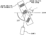
각 실시예 및 각 비교예의 결정화 인듐 주석 복합 산화물층 (7) 의 잔류 응력 σ1 을, X 선 산란법에 의해 결정화 인듐 주석 복합 산화물층 (7) 의 결정 격자 변형으로부터 간접적으로 구하였다.The residual stress? 1 of the crystallized indium tin
분말 X 선 회절 장치 (리가크 제조) 에 의해, 측정 산란각 2θ = 59 ∼ 62°의 범위에서 0.04°간격으로 회절 강도를 측정하였다. 각 측정 각도에 있어서의 적산 시간 (노광 시간) 은 100 초로 하였다.The diffraction intensity was measured by a powder X-ray diffraction apparatus (manufactured by Rigaku Corporation) at intervals of 0.04 degrees in the range of the measured
그리고, 얻어진 회절 이미지의 피크 (인듐 주석 복합 산화물의 (622) 면의 피크) 각 2θ, 및 X 선원의 파장 λ 로부터 결정화 인듐 주석 복합 산화물층 (7) 의 결정 격자 간격 d 를 산출하고, d 를 토대로 격자 변형 ε 를 산출하였다. 산출에 있어서는 하기 식 (1), (2) 를 사용하였다.Then, the crystal lattice spacing d of the crystallized indium tin

λ 는 X 선원 (Cu Kα선) 의 파장 (= 0.15418 nm) 이고, d0 는 무응력 상태의 인듐 주석 복합 산화물의 격자면 간격 (= 0.15241 nm) 이다. 또, d0 는 ICDD (The International Centre for Diffraction Data) 데이터 베이스로부터 취득한 값이다.lambda is the wavelength (= 0.15418 nm) of the X-ray source (Cu K? ray), and d 0 is the lattice spacing (= 0.15241 nm) of the indium tin complex oxide without stress. Also, d 0 is a value obtained from an ICDD (International Center for Diffraction Data) database.
상기 X 선 회절 측정을, 도 3 에 나타내는 필름면 법선과 인듐 주석 복합 산화물의 결정면 법선이 이루는 각도 Ψ 가 45°, 50°, 55°, 60°, 65°, 70°, 77°, 90°인 각각에 대해서 실시하고, 각각의 각도 Ψ 에 있어서의 격자 변형 ε 를 산출하였다. 또, 필름면 법선과 인듐 주석 복합 산화물의 결정면 법선이 이루는 각도 Ψ 는, TD 방향 (MD 방향과 직교하는 방향) 을 회전축 중심으로 하여 결정화 인듐 주석 복합 산화물층 (7) 을 회전시킴으로써, 조정하였다. 결정화 인듐 주석 복합 산화물층 (7) 의 면내 방향의 잔류 응력 σ1 은, sin2Ψ 와 격자 변형 ε 의 관계를 플롯한 직선의 기울기로부터 하기 식 (3) 에 의해 구하였다.The X-ray diffraction measurement was carried out at an angle of 45 °, 50 °, 55 °, 60 °, 65 °, 70 °, 77 ° and 90 ° formed by the plane surface normal of the film plane normal and the crystal plane normal of the indium tin complex oxide shown in FIG. , And the lattice strain epsilon at each angle [psi] was calculated. The angle? Made by the normal to the crystal plane of the indium tin composite oxide film plane and the film plane normal was adjusted by rotating the crystallized indium tin

상기 식에 있어서, E 는 인듐 주석 복합 산화물의 영률 (116GPa), ν 는 포와송 비 (0.35) 이다. 이들 값은, D. G. Neerinckand T. J. Vink, "Depthprofiling of thin ITO films by grazing incidence X-ray diffraction", Thin Solid Films, 278 (1996), PP 12-17. 에 기재되어 있는 이미 알려진 실측값이다.In the above equation, E is the Young's modulus (116 GPa) of the indium tin composite oxide, and v is Poisson's ratio (0.35). These values are described in D. G. Neerinckand T. J. Vink, "Depth Profiling of thin ITO films by grazing incidence X-ray diffraction ", Thin Solid Films, 278 (1996), PP 12-17. Which is already known.
실시예 2 및 4 에 대해서는, 잔류 응력을 최소 잔류 응력 σ2 로서 구하였다.For Examples 2 and 4, the residual stress was obtained as the minimum residual stress? 2.
(수축률 SR) (Shrinkage ratio SR)
각 실시예 및 각 비교예에 있어서의 제 2 공정 직후의 결정화 필름 (11) 의 MD 방향의 수축률 SR1 을 평가하였다.The shrinkage ratio SR1 in the MD direction of the crystallized
구체적으로는 먼저, 도 1A 에 나타내는 제조 도중의 비정질 필름 (1) 을, 폭 100 mm, 길이 100 mm 로 절취하여 (시험편), MD 방향에 있어서 80 mm 마다 표시를 하고, MD 방향의 길이 (㎜) 를 올림푸스 디지털식 소형 측정 현미경 STM5 (올림푸스 광학 공업 (주) 제조) 에 의해 정밀하게 측정하였다. 그 후, 표 1 에 기재된 결정화 조건에서 가열하여, 결정화 인듐 주석 복합 산화물층 (7) 을 구비하는 결정화 필름 (11) 을 제조하였다.Concretely, first, the
그 후, 결정화 필름 (11) 을 25 ℃ (상온) 에서 1 시간 방랭 후, 재차, 결정화 필름 (11) 의 MD 방향의 길이를 측정하였다.Thereafter, the
그리고, 하기 식에 의거하여 수축률 SR1 을 산출하였다.Then, the shrinkage ratio SR1 was calculated based on the following formula.
수축률 SR1 (%) = 〔[가열 전의 표시 간의 MD 방향 길이 (㎜)-가열 후의 표시 간의 MD 방향 (㎜)]/가열 전의 표시 간의 MD 방향 (㎜)〕× 100Shrinkage Ratio SR1 (%) = [[MD direction length (mm) between displays before heating-MD direction (mm) between displays after heating] / MD direction (mm)
또한, 실시예 2 및 실시예 4 에 대해서는, 수축률을 최소 수축률 SR2 로서 산출하였다.For Examples 2 and 4, the shrinkage ratio was calculated as the minimum shrinkage ratio SR2.
(분위기를 25 ℃ 및 10 % RH 로부터 85 ℃, 85 % RH 로 변동시켰을 때 일정한 인장 하중하에 있어서의 결정화 필름의 신장률 EP)(Elongation EP of the crystallized film under a constant tensile load when the atmosphere was changed from 25 ° C and 10% RH to 85 ° C and 85% RH)
각 실시예 및 각 비교예를 일정한 인장 하중하에 있어서의 결정화 필름 (11) 에 대해서 열분석 장치 (TMA, 주식회사 Seiko 사 제조) 를 사용하며, 25 ℃ 및 10 % RH 분위기하로부터 85 ℃ 및 85 % RH 분위기하로 변동시켰을 때 신장률 EP1 을 구하였다.(TMA, manufactured by Seiko Co., Ltd.) was used for the crystallized
구체적으로는 비교예 1 및 실시예 1, 2 의 결정화 필름 (11) (등방성의 투명 필름 기재 (2) 를 구비하는 결정화 필름 (11)) 을, MD 방향이 길이 방향을 따르도록 150 mm × 10 mm 로 절취하여 시험편을 제작하였다. 또한, 비교예 2 및 실시예 3, 4 의 결정화 필름 (11) (복굴절성의 투명 필름 기재 (2) 를 구비하는 결정화 필름 (11)) 을, MD 방향 및 TD 방향에 대하여 45 도를 이루는 방향이 길이 방향을 따르도록 150 mm × 10 mm 로 절취하여 시험편을 제작하였다.Specifically, the
이어서, 시험편에, 길이 방향으로 20 mN 의 일정한 인장 하중을 가면서, 분위기를 25 ℃ 및 10 % RH 로부터 85 ℃ 및 85 % RH 로 가열 (가열 속도 : 1 ℃/분) 및 가습 (가습 속도 : 5 % RH/분) 시켰을 때 결정화 필름 (11) 의 신장률 EP1 을 이하의 식을 사용하여 구하였다.Subsequently, the test piece was heated from 25 占 폚 and 10% RH to 85 占 폚 and 85% RH (heating rate: 1 占 폚 / min) and humidified (humidification rate: 5 % RH / min), the elongation EP1 of the crystallized
신장률 (%) = 신장량 (㎜)/150 (㎜) × 100Elongation (%) = elongation (mm) / 150 (mm) x 100
신장량 = 가열 가습 전의 결정화 필름 (11) 의 인장 방향 길이 (㎜)-150 (㎜)Elongation amount = length (mm) in tensile direction of
또, 실시예 2 및 4 에 대해서는, 신장률을 최대 신장률 EP2 로서 구하였다.In Examples 2 and 4, the elongation percentage was determined as the maximum elongation percentage EP2.
(크랙 억제 시험)(Crack inhibition test)
결정화 인듐 주석 복합 산화물층 (7) 의 상면에, 두께 1.3 mm 의 유리층 (9) (도 1B 가상선) 을, 두께 50 ㎛ 의 감압 접착제층 (8) (도 1B 가상선) 을 통해서 접착시켰다. 이로써, 결정화 필름 (11), 감압 접착제층 (8) 및 유리층 (9) 을 구비하는 결정화 필름 적층체 (10) 를 제조하였다.A glass layer 9 (a virtual line in Fig. 1B) having a thickness of 1.3 mm was bonded to the upper surface of the crystallized indium tin
그 후, 결정화 필름 적층체 (10) 를, 85 ℃, 85 % RH 의 환경하에 두고, 120 시간마다 취출하여, 현미경으로 결정화 인듐 주석 복합 산화물층 (7) 의 크랙 유무를 확인하였다.Thereafter, the crystallized
그리고, 하기 기준에 따라 단시간 (240 시간) 에 있어서의 크랙 억제를 평가하였다.Crack inhibition was evaluated in a short time (240 hours) according to the following criteria.
○ : 크랙의 발생 시간이 240 시간 초과였다. 요컨대, 240 시간 이하에서는, 크랙을 억제할 수 있었다.?: The occurrence time of the crack exceeded 240 hours. In short, at 240 hours or less, cracks could be suppressed.
× : 크랙의 발생 시간이 240 시간 이하였다.X: The occurrence time of the crack was 240 hours or less.

Claims (3)
상기 결정화 필름은, 투명 필름 기재 및 비정질 인듐 주석 복합 산화물층을 구비하는 비정질 필름을 특정 온도에서 결정화시킴으로써 얻어지는 특정 온도 결정화 필름으로서,
상기 특정 온도 결정화 필름에 있어서의 결정화 인듐 주석 복합 산화물층의 잔류 응력 σ1 과, 상기 비정질 필름을 110 ℃ 에서 결정화시킴으로써 얻어지는 110 ℃ 결정화 필름에 있어서의 결정화 인듐 주석 복합 산화물층의 잔류 응력 σ2 의 차이가, 150 MPa 이하인 것을 특징으로 하는, 결정화 필름.A transparent film substrate and a crystallized indium tin composite oxide layer,
The crystallization film is a specific temperature-crystallized film obtained by crystallizing an amorphous film having a transparent film base and an amorphous indium tin composite oxide layer at a specific temperature,
The residual stress σ1 of the indium tin oxide complex oxide layer in the specific temperature-crystallized film and the residual stress σ2 of the indium tin complex oxide layer in the 110 캜 crystallized film obtained by crystallizing the amorphous film at 110 캜 , And 150 MPa or less.
상기 특정 온도 결정화 필름은, 상기 비정질 필름의 상기 특정 온도에서의 가열에 의해 상기 비정질 필름에 대하여 수축되어 있고,
상기 110 ℃ 결정화 필름은, 상기 비정질 필름의 110 ℃ 에서의 가열에 의해 상기 비정질 필름에 대하여 수축되어 있고,
상기 특정 온도 결정화 필름의 수축률 SR1 과 상기 110 ℃ 결정화 필름의 수축률 SR2 의 차이가, 0.05 % 이하인 것을 특징으로 하는, 결정화 필름.The method according to claim 1,
The specific temperature-crystallized film is shrunk to the amorphous film by heating at the specific temperature of the amorphous film,
The 110 占 폚 crystallized film is shrunk to the amorphous film by heating at 110 占 폚 of the amorphous film,
Wherein the difference between the shrinkage ratio SR1 of the specific temperature-crystallized film and the shrinkage ratio SR2 of the 110 DEG C crystallization film is 0.05% or less.
상기 특정 온도 결정화 필름 및 상기 110 ℃ 결정화 필름은 모두 일정한 인장 하중하에서, 25 ℃ 및 10 % RH 로부터 85 ℃ 및 85 % RH 로 가열 및 가습될 때에 신장되고,
상기 특정 온도 결정화 필름의 신장률 EP1 과 상기 110 ℃ 결정화 필름의 신장률 EP2 의 차이가, 0.07 % 이하인 것을 특징으로 하는, 결정화 필름.The method according to claim 1,
Both the specific temperature-crystallized film and the 110 ° C crystallized film are elongated when they are heated and humidified at 25 ° C and 10% RH at 85 ° C and 85% RH under a constant tensile load,
Wherein the difference between the elongation percentage EP1 of the specific temperature-crystallized film and the elongation percentage EP2 of the 110 DEG C crystallized film is 0.07% or less.
Applications Claiming Priority (2)
| Application Number | Priority Date | Filing Date | Title |
|---|---|---|---|
| JPJP-P-2017-186764 | 2017-09-27 | ||
| JP2017186764A JP2019059170A (en) | 2017-09-27 | 2017-09-27 | Crystallization film |
Publications (1)
| Publication Number | Publication Date |
|---|---|
| KR20190036475A true KR20190036475A (en) | 2019-04-04 |
Family
ID=65864699
Family Applications (1)
| Application Number | Title | Priority Date | Filing Date |
|---|---|---|---|
| KR1020180109321A KR20190036475A (en) | 2017-09-27 | 2018-09-13 | Crystallization film |
Country Status (4)
| Country | Link |
|---|---|
| JP (1) | JP2019059170A (en) |
| KR (1) | KR20190036475A (en) |
| CN (1) | CN109559842A (en) |
| TW (1) | TW201916064A (en) |
Families Citing this family (2)
| Publication number | Priority date | Publication date | Assignee | Title |
|---|---|---|---|---|
| CN115315758B (en) * | 2020-03-19 | 2024-03-19 | 日东电工株式会社 | Transparent conductive film |
| JP2022072607A (en) * | 2020-10-30 | 2022-05-17 | 日東電工株式会社 | Method for manufacturing laminate film and strain sensor |
Family Cites Families (8)
| Publication number | Priority date | Publication date | Assignee | Title |
|---|---|---|---|---|
| JP2002150842A (en) * | 2000-11-15 | 2002-05-24 | Kanegafuchi Chem Ind Co Ltd | Polymer film with transparent conductive film |
| JP4882262B2 (en) * | 2005-03-31 | 2012-02-22 | 凸版印刷株式会社 | Method for producing transparent conductive film laminate |
| WO2012005300A1 (en) * | 2010-07-06 | 2012-01-12 | 日東電工株式会社 | Transparent conductive film and manufacturing method therefor |
| JP6031559B2 (en) * | 2010-12-27 | 2016-11-24 | 日東電工株式会社 | Transparent conductive film and method for producing the same |
| JP5196001B2 (en) * | 2011-09-29 | 2013-05-15 | 東洋紡株式会社 | Transparent conductive film and method for producing the same |
| WO2015080496A1 (en) * | 2013-11-27 | 2015-06-04 | 주식회사 엘지화학 | Conductive structure precursor, conductive structure and manufacturing method therefor |
| JP2015146244A (en) * | 2014-02-03 | 2015-08-13 | 凸版印刷株式会社 | Transparent conductive film and manufacturing method thereof |
| WO2015178298A1 (en) * | 2014-05-20 | 2015-11-26 | 日東電工株式会社 | Transparent conductive film and method for producing same |
-
2017
- 2017-09-27 JP JP2017186764A patent/JP2019059170A/en active Pending
-
2018
- 2018-09-13 KR KR1020180109321A patent/KR20190036475A/en unknown
- 2018-09-25 TW TW107133583A patent/TW201916064A/en unknown
- 2018-09-26 CN CN201811125171.1A patent/CN109559842A/en active Pending
Also Published As
| Publication number | Publication date |
|---|---|
| JP2019059170A (en) | 2019-04-18 |
| TW201916064A (en) | 2019-04-16 |
| CN109559842A (en) | 2019-04-02 |
Similar Documents
| Publication | Publication Date | Title |
|---|---|---|
| KR101991545B1 (en) | Transparent electroconductive film and manufacturing method therefor | |
| US9260777B2 (en) | Transparent crystalline electrically-conductive thin film, method of production thereof, transparent electrically-conductive film, and touch panel | |
| JP6523357B2 (en) | Transparent conductive film and method for producing the same | |
| WO2012086484A1 (en) | Transparent electroconductive film and manufacturing method therefor | |
| JP6181806B2 (en) | Transparent conductive film and method for producing the same | |
| KR20130025969A (en) | Transparent conductive film and manufacturing method therefor | |
| JP6650770B2 (en) | Conductive laminated film | |
| KR20170090352A (en) | Transparent conductive film with protective film | |
| JP7278372B2 (en) | transparent conductive film | |
| JP2009073090A (en) | Functional film, manufacturing method of functional film, laminated body, and electronic device | |
| KR20190036475A (en) | Crystallization film | |
| CN110197739B (en) | Transparent conductive film laminate and method for producing transparent conductive film | |
| JP2015191347A (en) | Transparent conductive film laminate and method for manufacturing touch panel | |
| JP2020108941A (en) | Transparent conductive film laminate | |
| JP2005018551A (en) | Touch panel having electromagnetic wave shielding function and transparent lamination film to be used for touch panel | |
| JP7270334B2 (en) | Transparent conductive film and manufacturing method thereof | |
| CN111696702A (en) | Thin film laminate and method for producing patterned conductive thin film | |
| CN111696703A (en) | Thin film laminate and method for producing patterned conductive thin film | |
| KR20190042438A (en) | Method for producing an inorganic layer laminate | |
| JP5722473B2 (en) | Transparent conductive film | |
| WO2020262047A1 (en) | Crystallized indium tin composite oxide film, transparent electric conductive film, and production method therefor | |
| WO2020262284A1 (en) | Transparent conductive film | |
| JP2023013411A (en) | Transparent conductive laminate and transparent conductive film |