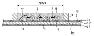
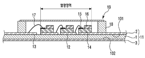
KR20140047750A - 발광 장치 - Google Patents
발광 장치 Download PDFInfo
- Publication number
- KR20140047750A KR20140047750A KR1020120111596A KR20120111596A KR20140047750A KR 20140047750 A KR20140047750 A KR 20140047750A KR 1020120111596 A KR1020120111596 A KR 1020120111596A KR 20120111596 A KR20120111596 A KR 20120111596A KR 20140047750 A KR20140047750 A KR 20140047750A
- Authority
- KR
- South Korea
- Prior art keywords
- light emitting
- substrate
- emitting device
- front surface
- electrode pattern
- Prior art date
- Legal status (The legal status is an assumption and is not a legal conclusion. Google has not performed a legal analysis and makes no representation as to the accuracy of the status listed.)
- Ceased
Links
Images
Classifications
-
- H—ELECTRICITY
- H10—SEMICONDUCTOR DEVICES; ELECTRIC SOLID-STATE DEVICES NOT OTHERWISE PROVIDED FOR
- H10H—INORGANIC LIGHT-EMITTING SEMICONDUCTOR DEVICES HAVING POTENTIAL BARRIERS
- H10H20/00—Individual inorganic light-emitting semiconductor devices having potential barriers, e.g. light-emitting diodes [LED]
- H10H20/80—Constructional details
- H10H20/85—Packages
- H10H20/852—Encapsulations
- H10H20/854—Encapsulations characterised by their material, e.g. epoxy or silicone resins
-
- H—ELECTRICITY
- H01—ELECTRIC ELEMENTS
- H01L—SEMICONDUCTOR DEVICES NOT COVERED BY CLASS H10
- H01L25/00—Assemblies consisting of a plurality of semiconductor or other solid state devices
- H01L25/03—Assemblies consisting of a plurality of semiconductor or other solid state devices all the devices being of a type provided for in a single subclass of subclasses H10B, H10D, H10F, H10H, H10K or H10N, e.g. assemblies of rectifier diodes
- H01L25/04—Assemblies consisting of a plurality of semiconductor or other solid state devices all the devices being of a type provided for in a single subclass of subclasses H10B, H10D, H10F, H10H, H10K or H10N, e.g. assemblies of rectifier diodes the devices not having separate containers
- H01L25/075—Assemblies consisting of a plurality of semiconductor or other solid state devices all the devices being of a type provided for in a single subclass of subclasses H10B, H10D, H10F, H10H, H10K or H10N, e.g. assemblies of rectifier diodes the devices not having separate containers the devices being of a type provided for in group H10H20/00
- H01L25/0753—Assemblies consisting of a plurality of semiconductor or other solid state devices all the devices being of a type provided for in a single subclass of subclasses H10B, H10D, H10F, H10H, H10K or H10N, e.g. assemblies of rectifier diodes the devices not having separate containers the devices being of a type provided for in group H10H20/00 the devices being arranged next to each other
-
- H—ELECTRICITY
- H10—SEMICONDUCTOR DEVICES; ELECTRIC SOLID-STATE DEVICES NOT OTHERWISE PROVIDED FOR
- H10H—INORGANIC LIGHT-EMITTING SEMICONDUCTOR DEVICES HAVING POTENTIAL BARRIERS
- H10H20/00—Individual inorganic light-emitting semiconductor devices having potential barriers, e.g. light-emitting diodes [LED]
- H10H20/80—Constructional details
- H10H20/85—Packages
- H10H20/858—Means for heat extraction or cooling
- H10H20/8581—Means for heat extraction or cooling characterised by their material
-
- H—ELECTRICITY
- H10—SEMICONDUCTOR DEVICES; ELECTRIC SOLID-STATE DEVICES NOT OTHERWISE PROVIDED FOR
- H10H—INORGANIC LIGHT-EMITTING SEMICONDUCTOR DEVICES HAVING POTENTIAL BARRIERS
- H10H29/00—Integrated devices, or assemblies of multiple devices, comprising at least one light-emitting semiconductor element covered by group H10H20/00
- H10H29/10—Integrated devices comprising at least one light-emitting semiconductor component covered by group H10H20/00
-
- H—ELECTRICITY
- H01—ELECTRIC ELEMENTS
- H01L—SEMICONDUCTOR DEVICES NOT COVERED BY CLASS H10
- H01L2224/00—Indexing scheme for arrangements for connecting or disconnecting semiconductor or solid-state bodies and methods related thereto as covered by H01L24/00
- H01L2224/01—Means for bonding being attached to, or being formed on, the surface to be connected, e.g. chip-to-package, die-attach, "first-level" interconnects; Manufacturing methods related thereto
- H01L2224/42—Wire connectors; Manufacturing methods related thereto
- H01L2224/47—Structure, shape, material or disposition of the wire connectors after the connecting process
- H01L2224/48—Structure, shape, material or disposition of the wire connectors after the connecting process of an individual wire connector
- H01L2224/4805—Shape
- H01L2224/4809—Loop shape
- H01L2224/48091—Arched
-
- H—ELECTRICITY
- H10—SEMICONDUCTOR DEVICES; ELECTRIC SOLID-STATE DEVICES NOT OTHERWISE PROVIDED FOR
- H10H—INORGANIC LIGHT-EMITTING SEMICONDUCTOR DEVICES HAVING POTENTIAL BARRIERS
- H10H20/00—Individual inorganic light-emitting semiconductor devices having potential barriers, e.g. light-emitting diodes [LED]
- H10H20/80—Constructional details
- H10H20/85—Packages
- H10H20/855—Optical field-shaping means, e.g. lenses
-
- H—ELECTRICITY
- H10—SEMICONDUCTOR DEVICES; ELECTRIC SOLID-STATE DEVICES NOT OTHERWISE PROVIDED FOR
- H10H—INORGANIC LIGHT-EMITTING SEMICONDUCTOR DEVICES HAVING POTENTIAL BARRIERS
- H10H20/00—Individual inorganic light-emitting semiconductor devices having potential barriers, e.g. light-emitting diodes [LED]
- H10H20/80—Constructional details
- H10H20/85—Packages
- H10H20/857—Interconnections, e.g. lead-frames, bond wires or solder balls
Landscapes
- Engineering & Computer Science (AREA)
- Power Engineering (AREA)
- Microelectronics & Electronic Packaging (AREA)
- Physics & Mathematics (AREA)
- Condensed Matter Physics & Semiconductors (AREA)
- General Physics & Mathematics (AREA)
- Computer Hardware Design (AREA)
- Led Device Packages (AREA)
- Fastening Of Light Sources Or Lamp Holders (AREA)
Priority Applications (5)
| Application Number | Priority Date | Filing Date | Title |
|---|---|---|---|
| KR1020120111596A KR20140047750A (ko) | 2012-10-09 | 2012-10-09 | 발광 장치 |
| US14/010,592 US9093626B2 (en) | 2012-10-09 | 2013-08-27 | Luminescence device |
| JP2013183879A JP2014078695A (ja) | 2012-10-09 | 2013-09-05 | 発光装置 |
| EP13184243.7A EP2720266B1 (en) | 2012-10-09 | 2013-09-13 | Luminescence device |
| CN201310467515.8A CN103715338A (zh) | 2012-10-09 | 2013-10-09 | 发光器件 |
Applications Claiming Priority (1)
| Application Number | Priority Date | Filing Date | Title |
|---|---|---|---|
| KR1020120111596A KR20140047750A (ko) | 2012-10-09 | 2012-10-09 | 발광 장치 |
Publications (1)
| Publication Number | Publication Date |
|---|---|
| KR20140047750A true KR20140047750A (ko) | 2014-04-23 |
Family
ID=49212592
Family Applications (1)
| Application Number | Title | Priority Date | Filing Date |
|---|---|---|---|
| KR1020120111596A Ceased KR20140047750A (ko) | 2012-10-09 | 2012-10-09 | 발광 장치 |
Country Status (5)
| Country | Link |
|---|---|
| US (1) | US9093626B2 (enExample) |
| EP (1) | EP2720266B1 (enExample) |
| JP (1) | JP2014078695A (enExample) |
| KR (1) | KR20140047750A (enExample) |
| CN (1) | CN103715338A (enExample) |
Families Citing this family (5)
| Publication number | Priority date | Publication date | Assignee | Title |
|---|---|---|---|---|
| TWI548005B (zh) * | 2014-01-24 | 2016-09-01 | 環旭電子股份有限公司 | 選擇性電子封裝模組的製造方法 |
| US10978619B2 (en) * | 2016-12-02 | 2021-04-13 | Toyoda Gosei Co., Ltd. | Light emitting device |
| JP2018098085A (ja) * | 2016-12-15 | 2018-06-21 | 株式会社ジャパンディスプレイ | 表示装置 |
| CN107369741A (zh) * | 2017-07-13 | 2017-11-21 | 东莞市凯昶德电子科技股份有限公司 | 带一体式金属围坝的led支架模组及其制备方法 |
| JP7053249B2 (ja) * | 2017-12-22 | 2022-04-12 | スタンレー電気株式会社 | 半導体発光装置 |
Citations (3)
| Publication number | Priority date | Publication date | Assignee | Title |
|---|---|---|---|---|
| JP2008300350A (ja) * | 2007-05-02 | 2008-12-11 | Cree Inc | Criの高い暖色系白色光を供給するマルチチップ発光デバイスランプおよびこれを含む照明器具 |
| JP2011071407A (ja) * | 2009-09-28 | 2011-04-07 | Sharp Corp | 発光素子および照明装置 |
| JP2011113672A (ja) * | 2009-11-24 | 2011-06-09 | Toshiba Lighting & Technology Corp | 発光装置及びこれを備えた照明器具 |
Family Cites Families (14)
| Publication number | Priority date | Publication date | Assignee | Title |
|---|---|---|---|---|
| US6384473B1 (en) * | 2000-05-16 | 2002-05-07 | Sandia Corporation | Microelectronic device package with an integral window |
| JP2002305261A (ja) * | 2001-01-10 | 2002-10-18 | Canon Inc | 電子部品及びその製造方法 |
| JP2005317599A (ja) * | 2004-04-27 | 2005-11-10 | Kyocera Corp | 電子部品搭載用基板および電子装置 |
| US7170100B2 (en) * | 2005-01-21 | 2007-01-30 | Luminus Devices, Inc. | Packaging designs for LEDs |
| EP1909336B1 (en) * | 2005-06-30 | 2014-10-22 | Panasonic Corporation | Light emitting device |
| US8735920B2 (en) * | 2006-07-31 | 2014-05-27 | Cree, Inc. | Light emitting diode package with optical element |
| US7943952B2 (en) * | 2006-07-31 | 2011-05-17 | Cree, Inc. | Method of uniform phosphor chip coating and LED package fabricated using method |
| TWI367465B (en) * | 2008-02-15 | 2012-07-01 | Foxsemicon Integrated Tech Inc | Led display |
| KR20100079688A (ko) * | 2008-12-31 | 2010-07-08 | 서울반도체 주식회사 | Led 패키지 |
| CN102074558B (zh) * | 2009-10-21 | 2013-06-19 | 东芝照明技术株式会社 | 发光装置以及照明器具 |
| EP2315284A3 (en) * | 2009-10-21 | 2013-03-27 | Toshiba Lighting & Technology Corporation | Light-Emitting apparatus and luminaire |
| EP2378576A2 (en) * | 2010-04-15 | 2011-10-19 | Samsung LED Co., Ltd. | Light emitting diode package, lighting apparatus having the same, and method for manufacturing light emitting diode package |
| EP2448028B1 (en) * | 2010-10-29 | 2017-05-31 | Nichia Corporation | Light emitting apparatus and production method thereof |
| KR101901890B1 (ko) * | 2012-09-28 | 2018-09-28 | 엘지이노텍 주식회사 | 발광 장치 |
-
2012
- 2012-10-09 KR KR1020120111596A patent/KR20140047750A/ko not_active Ceased
-
2013
- 2013-08-27 US US14/010,592 patent/US9093626B2/en active Active
- 2013-09-05 JP JP2013183879A patent/JP2014078695A/ja active Pending
- 2013-09-13 EP EP13184243.7A patent/EP2720266B1/en not_active Not-in-force
- 2013-10-09 CN CN201310467515.8A patent/CN103715338A/zh active Pending
Patent Citations (3)
| Publication number | Priority date | Publication date | Assignee | Title |
|---|---|---|---|---|
| JP2008300350A (ja) * | 2007-05-02 | 2008-12-11 | Cree Inc | Criの高い暖色系白色光を供給するマルチチップ発光デバイスランプおよびこれを含む照明器具 |
| JP2011071407A (ja) * | 2009-09-28 | 2011-04-07 | Sharp Corp | 発光素子および照明装置 |
| JP2011113672A (ja) * | 2009-11-24 | 2011-06-09 | Toshiba Lighting & Technology Corp | 発光装置及びこれを備えた照明器具 |
Also Published As
| Publication number | Publication date |
|---|---|
| US9093626B2 (en) | 2015-07-28 |
| JP2014078695A (ja) | 2014-05-01 |
| EP2720266A2 (en) | 2014-04-16 |
| CN103715338A (zh) | 2014-04-09 |
| EP2720266B1 (en) | 2021-10-20 |
| US20140097452A1 (en) | 2014-04-10 |
| EP2720266A3 (en) | 2016-03-16 |
Similar Documents
| Publication | Publication Date | Title |
|---|---|---|
| JP5999929B2 (ja) | 発光素子パッケージ及びこれを利用した照明システム | |
| CN101779303B (zh) | 半导体发光器件及包括该半导体发光器件的光源装置和照明系统 | |
| KR101088910B1 (ko) | Led 패키지 및 그 제조방법 | |
| JP6583764B2 (ja) | 発光装置、及び照明装置 | |
| JP2016058614A (ja) | 発光装置、及び照明装置 | |
| JP2017162942A (ja) | 発光装置、及び、照明装置 | |
| TWI496323B (zh) | 發光模組 | |
| KR20140047750A (ko) | 발광 장치 | |
| JP2018129492A (ja) | 発光装置、及び、照明装置 | |
| KR101901890B1 (ko) | 발광 장치 | |
| KR20140004351A (ko) | 발광 다이오드 패키지 | |
| JP2008244468A (ja) | 発光装置 | |
| JP5406691B2 (ja) | 半導体発光装置 | |
| JP2017034134A (ja) | 発光装置、及び、照明装置 | |
| JP2014140050A (ja) | 発光装置 | |
| JP5779220B2 (ja) | 蛍光体及びこれを備えた発光素子 | |
| KR20110125067A (ko) | 발광소자 패키지 | |
| KR102000072B1 (ko) | 발광 장치 | |
| JP2009278012A (ja) | Led装置用パッケージ | |
| KR20110108097A (ko) | 발광소자 패키지 및 이를 포함하는 조명시스템 | |
| JP2010225607A (ja) | 発光装置 | |
| KR102424726B1 (ko) | 발광 소자 패키지 | |
| CN103715186A (zh) | 用于产生对称性均匀混光光源的多芯片封装结构 | |
| KR20150035620A (ko) | 칩 온 보드 발광 다이오드 모듈 | |
| JP2019021744A (ja) | 発光装置、及び、照明装置 |
Legal Events
| Date | Code | Title | Description |
|---|---|---|---|
| PA0109 | Patent application |
Patent event code: PA01091R01D Comment text: Patent Application Patent event date: 20121009 |
|
| PG1501 | Laying open of application | ||
| A201 | Request for examination | ||
| PA0201 | Request for examination |
Patent event code: PA02012R01D Patent event date: 20170920 Comment text: Request for Examination of Application Patent event code: PA02011R01I Patent event date: 20121009 Comment text: Patent Application |
|
| E902 | Notification of reason for refusal | ||
| PE0902 | Notice of grounds for rejection |
Comment text: Notification of reason for refusal Patent event date: 20180612 Patent event code: PE09021S01D |
|
| E601 | Decision to refuse application | ||
| PE0601 | Decision on rejection of patent |
Patent event date: 20181226 Comment text: Decision to Refuse Application Patent event code: PE06012S01D Patent event date: 20180612 Comment text: Notification of reason for refusal Patent event code: PE06011S01I |


