KR20140001896A - Ceramic capacitor and methods of manufacture - Google Patents
Ceramic capacitor and methods of manufacture Download PDFInfo
- Publication number
- KR20140001896A KR20140001896A KR1020137012334A KR20137012334A KR20140001896A KR 20140001896 A KR20140001896 A KR 20140001896A KR 1020137012334 A KR1020137012334 A KR 1020137012334A KR 20137012334 A KR20137012334 A KR 20137012334A KR 20140001896 A KR20140001896 A KR 20140001896A
- Authority
- KR
- South Korea
- Prior art keywords
- dielectric
- metal
- layer
- capacitor
- dielectric layer
- Prior art date
Links
- 238000000034 method Methods 0.000 title claims abstract description 76
- 238000004519 manufacturing process Methods 0.000 title description 34
- 239000003985 ceramic capacitor Substances 0.000 title description 12
- 229910052751 metal Inorganic materials 0.000 claims abstract description 238
- 239000002184 metal Substances 0.000 claims abstract description 237
- 239000003990 capacitor Substances 0.000 claims abstract description 173
- 238000005245 sintering Methods 0.000 claims abstract description 85
- 239000002245 particle Substances 0.000 claims abstract description 66
- 239000002131 composite material Substances 0.000 claims abstract description 64
- 238000000576 coating method Methods 0.000 claims abstract description 55
- 239000011248 coating agent Substances 0.000 claims abstract description 40
- 239000003989 dielectric material Substances 0.000 claims abstract description 36
- 238000011065 in-situ storage Methods 0.000 claims abstract description 19
- 239000000919 ceramic Substances 0.000 claims description 99
- 230000001747 exhibiting effect Effects 0.000 claims description 4
- 230000008878 coupling Effects 0.000 claims description 2
- 238000010168 coupling process Methods 0.000 claims description 2
- 238000005859 coupling reaction Methods 0.000 claims description 2
- 238000007667 floating Methods 0.000 claims description 2
- 238000000429 assembly Methods 0.000 abstract description 6
- 230000000712 assembly Effects 0.000 abstract description 6
- 238000007796 conventional method Methods 0.000 abstract 1
- 239000010410 layer Substances 0.000 description 356
- 229910052709 silver Inorganic materials 0.000 description 60
- BQCADISMDOOEFD-UHFFFAOYSA-N Silver Chemical compound [Ag] BQCADISMDOOEFD-UHFFFAOYSA-N 0.000 description 58
- 239000004332 silver Substances 0.000 description 58
- KDLHZDBZIXYQEI-UHFFFAOYSA-N Palladium Chemical compound [Pd] KDLHZDBZIXYQEI-UHFFFAOYSA-N 0.000 description 40
- PXHVJJICTQNCMI-UHFFFAOYSA-N Nickel Chemical compound [Ni] PXHVJJICTQNCMI-UHFFFAOYSA-N 0.000 description 32
- 239000000463 material Substances 0.000 description 27
- 239000004020 conductor Substances 0.000 description 26
- 238000004626 scanning electron microscopy Methods 0.000 description 22
- 239000000843 powder Substances 0.000 description 20
- 230000008569 process Effects 0.000 description 19
- 229910052759 nickel Inorganic materials 0.000 description 17
- 239000002002 slurry Substances 0.000 description 17
- 230000003287 optical effect Effects 0.000 description 15
- 229910052763 palladium Inorganic materials 0.000 description 15
- 239000000976 ink Substances 0.000 description 14
- BASFCYQUMIYNBI-UHFFFAOYSA-N platinum Chemical compound [Pt] BASFCYQUMIYNBI-UHFFFAOYSA-N 0.000 description 14
- 229910001252 Pd alloy Inorganic materials 0.000 description 13
- 239000010949 copper Substances 0.000 description 11
- 238000002844 melting Methods 0.000 description 11
- 230000008018 melting Effects 0.000 description 11
- SWELZOZIOHGSPA-UHFFFAOYSA-N palladium silver Chemical compound [Pd].[Ag] SWELZOZIOHGSPA-UHFFFAOYSA-N 0.000 description 11
- RYGMFSIKBFXOCR-UHFFFAOYSA-N Copper Chemical compound [Cu] RYGMFSIKBFXOCR-UHFFFAOYSA-N 0.000 description 10
- 229910052802 copper Inorganic materials 0.000 description 10
- 239000002923 metal particle Substances 0.000 description 10
- 238000007639 printing Methods 0.000 description 9
- 238000007650 screen-printing Methods 0.000 description 9
- -1 but not limited to Substances 0.000 description 8
- 238000013461 design Methods 0.000 description 8
- 239000000203 mixture Substances 0.000 description 8
- 238000002791 soaking Methods 0.000 description 8
- 229910002113 barium titanate Inorganic materials 0.000 description 7
- 230000005012 migration Effects 0.000 description 7
- 238000013508 migration Methods 0.000 description 7
- 229910052697 platinum Inorganic materials 0.000 description 7
- 229910001316 Ag alloy Inorganic materials 0.000 description 6
- ZOKXTWBITQBERF-UHFFFAOYSA-N Molybdenum Chemical compound [Mo] ZOKXTWBITQBERF-UHFFFAOYSA-N 0.000 description 6
- 229910000990 Ni alloy Inorganic materials 0.000 description 6
- 229910045601 alloy Inorganic materials 0.000 description 6
- 239000000956 alloy Substances 0.000 description 6
- 238000010304 firing Methods 0.000 description 6
- PCHJSUWPFVWCPO-UHFFFAOYSA-N gold Chemical compound [Au] PCHJSUWPFVWCPO-UHFFFAOYSA-N 0.000 description 6
- 229910052737 gold Inorganic materials 0.000 description 6
- 239000010931 gold Substances 0.000 description 6
- 239000012212 insulator Substances 0.000 description 6
- 229910052741 iridium Inorganic materials 0.000 description 6
- GKOZUEZYRPOHIO-UHFFFAOYSA-N iridium atom Chemical compound [Ir] GKOZUEZYRPOHIO-UHFFFAOYSA-N 0.000 description 6
- 229910052750 molybdenum Inorganic materials 0.000 description 6
- 239000011733 molybdenum Substances 0.000 description 6
- 229910052758 niobium Inorganic materials 0.000 description 6
- 239000010955 niobium Substances 0.000 description 6
- GUCVJGMIXFAOAE-UHFFFAOYSA-N niobium atom Chemical compound [Nb] GUCVJGMIXFAOAE-UHFFFAOYSA-N 0.000 description 6
- 239000010970 precious metal Substances 0.000 description 6
- 229910052715 tantalum Inorganic materials 0.000 description 6
- GUVRBAGPIYLISA-UHFFFAOYSA-N tantalum atom Chemical compound [Ta] GUVRBAGPIYLISA-UHFFFAOYSA-N 0.000 description 6
- WFKWXMTUELFFGS-UHFFFAOYSA-N tungsten Chemical compound [W] WFKWXMTUELFFGS-UHFFFAOYSA-N 0.000 description 6
- 229910052721 tungsten Inorganic materials 0.000 description 6
- 239000010937 tungsten Substances 0.000 description 6
- 229910000881 Cu alloy Inorganic materials 0.000 description 5
- JRPBQTZRNDNNOP-UHFFFAOYSA-N barium titanate Chemical compound [Ba+2].[Ba+2].[O-][Ti]([O-])([O-])[O-] JRPBQTZRNDNNOP-UHFFFAOYSA-N 0.000 description 5
- 239000010419 fine particle Substances 0.000 description 5
- 239000002241 glass-ceramic Substances 0.000 description 5
- XEEYBQQBJWHFJM-UHFFFAOYSA-N Iron Chemical compound [Fe] XEEYBQQBJWHFJM-UHFFFAOYSA-N 0.000 description 4
- PNEYBMLMFCGWSK-UHFFFAOYSA-N aluminium oxide Inorganic materials [O-2].[O-2].[O-2].[Al+3].[Al+3] PNEYBMLMFCGWSK-UHFFFAOYSA-N 0.000 description 4
- 239000011521 glass Substances 0.000 description 4
- 229910052735 hafnium Inorganic materials 0.000 description 4
- VBJZVLUMGGDVMO-UHFFFAOYSA-N hafnium atom Chemical compound [Hf] VBJZVLUMGGDVMO-UHFFFAOYSA-N 0.000 description 4
- 229910052809 inorganic oxide Inorganic materials 0.000 description 4
- 238000002156 mixing Methods 0.000 description 4
- 239000012811 non-conductive material Substances 0.000 description 4
- 229910052702 rhenium Inorganic materials 0.000 description 4
- WUAPFZMCVAUBPE-UHFFFAOYSA-N rhenium atom Chemical compound [Re] WUAPFZMCVAUBPE-UHFFFAOYSA-N 0.000 description 4
- 229910001260 Pt alloy Inorganic materials 0.000 description 3
- RTAQQCXQSZGOHL-UHFFFAOYSA-N Titanium Chemical compound [Ti] RTAQQCXQSZGOHL-UHFFFAOYSA-N 0.000 description 3
- 230000002776 aggregation Effects 0.000 description 3
- 238000004220 aggregation Methods 0.000 description 3
- 239000011324 bead Substances 0.000 description 3
- 230000015556 catabolic process Effects 0.000 description 3
- 150000001875 compounds Chemical class 0.000 description 3
- 239000011258 core-shell material Substances 0.000 description 3
- 238000011049 filling Methods 0.000 description 3
- 238000001465 metallisation Methods 0.000 description 3
- BPUBBGLMJRNUCC-UHFFFAOYSA-N oxygen(2-);tantalum(5+) Chemical compound [O-2].[O-2].[O-2].[O-2].[O-2].[Ta+5].[Ta+5] BPUBBGLMJRNUCC-UHFFFAOYSA-N 0.000 description 3
- 239000011236 particulate material Substances 0.000 description 3
- 238000000059 patterning Methods 0.000 description 3
- 239000003870 refractory metal Substances 0.000 description 3
- 229910001936 tantalum oxide Inorganic materials 0.000 description 3
- 238000010345 tape casting Methods 0.000 description 3
- 238000012360 testing method Methods 0.000 description 3
- 229910001020 Au alloy Inorganic materials 0.000 description 2
- KJTLSVCANCCWHF-UHFFFAOYSA-N Ruthenium Chemical compound [Ru] KJTLSVCANCCWHF-UHFFFAOYSA-N 0.000 description 2
- HCHKCACWOHOZIP-UHFFFAOYSA-N Zinc Chemical compound [Zn] HCHKCACWOHOZIP-UHFFFAOYSA-N 0.000 description 2
- QCWXUUIWCKQGHC-UHFFFAOYSA-N Zirconium Chemical compound [Zr] QCWXUUIWCKQGHC-UHFFFAOYSA-N 0.000 description 2
- 238000003491 array Methods 0.000 description 2
- 230000008901 benefit Effects 0.000 description 2
- 229910010293 ceramic material Inorganic materials 0.000 description 2
- 230000008859 change Effects 0.000 description 2
- 229910017052 cobalt Inorganic materials 0.000 description 2
- 239000010941 cobalt Substances 0.000 description 2
- GUTLYIVDDKVIGB-UHFFFAOYSA-N cobalt atom Chemical compound [Co] GUTLYIVDDKVIGB-UHFFFAOYSA-N 0.000 description 2
- 230000000052 comparative effect Effects 0.000 description 2
- 230000002950 deficient Effects 0.000 description 2
- 239000007772 electrode material Substances 0.000 description 2
- 239000003353 gold alloy Substances 0.000 description 2
- 229910052742 iron Inorganic materials 0.000 description 2
- WPBNNNQJVZRUHP-UHFFFAOYSA-L manganese(2+);methyl n-[[2-(methoxycarbonylcarbamothioylamino)phenyl]carbamothioyl]carbamate;n-[2-(sulfidocarbothioylamino)ethyl]carbamodithioate Chemical compound [Mn+2].[S-]C(=S)NCCNC([S-])=S.COC(=O)NC(=S)NC1=CC=CC=C1NC(=S)NC(=O)OC WPBNNNQJVZRUHP-UHFFFAOYSA-L 0.000 description 2
- 239000007769 metal material Substances 0.000 description 2
- 239000011859 microparticle Substances 0.000 description 2
- 238000012986 modification Methods 0.000 description 2
- 230000004048 modification Effects 0.000 description 2
- 238000000465 moulding Methods 0.000 description 2
- 229910052755 nonmetal Inorganic materials 0.000 description 2
- 238000000399 optical microscopy Methods 0.000 description 2
- 238000005325 percolation Methods 0.000 description 2
- 238000007747 plating Methods 0.000 description 2
- 238000012545 processing Methods 0.000 description 2
- 230000009467 reduction Effects 0.000 description 2
- 229910052703 rhodium Inorganic materials 0.000 description 2
- 239000010948 rhodium Substances 0.000 description 2
- MHOVAHRLVXNVSD-UHFFFAOYSA-N rhodium atom Chemical compound [Rh] MHOVAHRLVXNVSD-UHFFFAOYSA-N 0.000 description 2
- 229910052707 ruthenium Inorganic materials 0.000 description 2
- 239000002356 single layer Substances 0.000 description 2
- 239000002887 superconductor Substances 0.000 description 2
- 229910052719 titanium Inorganic materials 0.000 description 2
- 239000010936 titanium Substances 0.000 description 2
- 229910052725 zinc Inorganic materials 0.000 description 2
- 239000011701 zinc Substances 0.000 description 2
- 229910052726 zirconium Inorganic materials 0.000 description 2
- 241000220010 Rhode Species 0.000 description 1
- ATJFFYVFTNAWJD-UHFFFAOYSA-N Tin Chemical compound [Sn] ATJFFYVFTNAWJD-UHFFFAOYSA-N 0.000 description 1
- 239000000654 additive Substances 0.000 description 1
- 238000013459 approach Methods 0.000 description 1
- 239000010953 base metal Substances 0.000 description 1
- 239000011230 binding agent Substances 0.000 description 1
- 230000015572 biosynthetic process Effects 0.000 description 1
- 238000006243 chemical reaction Methods 0.000 description 1
- 230000000295 complement effect Effects 0.000 description 1
- 238000010276 construction Methods 0.000 description 1
- 230000003247 decreasing effect Effects 0.000 description 1
- 230000007547 defect Effects 0.000 description 1
- 230000032798 delamination Effects 0.000 description 1
- 238000000151 deposition Methods 0.000 description 1
- 230000008021 deposition Effects 0.000 description 1
- 238000010586 diagram Methods 0.000 description 1
- 238000009792 diffusion process Methods 0.000 description 1
- CJXLIMFTIKVMQN-UHFFFAOYSA-N dimagnesium;oxygen(2-);tantalum(5+) Chemical compound [O-2].[O-2].[O-2].[O-2].[O-2].[O-2].[O-2].[Mg+2].[Mg+2].[Ta+5].[Ta+5] CJXLIMFTIKVMQN-UHFFFAOYSA-N 0.000 description 1
- 238000007598 dipping method Methods 0.000 description 1
- 239000002270 dispersing agent Substances 0.000 description 1
- 238000009826 distribution Methods 0.000 description 1
- 239000002019 doping agent Substances 0.000 description 1
- 238000005553 drilling Methods 0.000 description 1
- 230000005684 electric field Effects 0.000 description 1
- 239000002003 electrode paste Substances 0.000 description 1
- 238000005516 engineering process Methods 0.000 description 1
- 239000010408 film Substances 0.000 description 1
- 238000001914 filtration Methods 0.000 description 1
- 230000005484 gravity Effects 0.000 description 1
- 238000005470 impregnation Methods 0.000 description 1
- 230000006872 improvement Effects 0.000 description 1
- 238000010952 in-situ formation Methods 0.000 description 1
- 238000009413 insulation Methods 0.000 description 1
- 230000010354 integration Effects 0.000 description 1
- 238000003475 lamination Methods 0.000 description 1
- 239000000320 mechanical mixture Substances 0.000 description 1
- 150000004706 metal oxides Chemical class 0.000 description 1
- 150000002739 metals Chemical class 0.000 description 1
- 229910000510 noble metal Inorganic materials 0.000 description 1
- 150000002843 nonmetals Chemical class 0.000 description 1
- 230000003647 oxidation Effects 0.000 description 1
- 238000007254 oxidation reaction Methods 0.000 description 1
- 239000004033 plastic Substances 0.000 description 1
- 229920006254 polymer film Polymers 0.000 description 1
- 229920000307 polymer substrate Polymers 0.000 description 1
- 239000002952 polymeric resin Substances 0.000 description 1
- 239000011148 porous material Substances 0.000 description 1
- 238000004080 punching Methods 0.000 description 1
- 238000003908 quality control method Methods 0.000 description 1
- 238000009877 rendering Methods 0.000 description 1
- 230000004044 response Effects 0.000 description 1
- 238000005096 rolling process Methods 0.000 description 1
- 229910000679 solder Inorganic materials 0.000 description 1
- 239000002904 solvent Substances 0.000 description 1
- 230000007480 spreading Effects 0.000 description 1
- 238000003892 spreading Methods 0.000 description 1
- 238000006467 substitution reaction Methods 0.000 description 1
- 239000000758 substrate Substances 0.000 description 1
- 239000002344 surface layer Substances 0.000 description 1
- 229920003002 synthetic resin Polymers 0.000 description 1
- 239000010409 thin film Substances 0.000 description 1
- 238000012546 transfer Methods 0.000 description 1
- 230000009466 transformation Effects 0.000 description 1
Images


Classifications
-
- H—ELECTRICITY
- H01—ELECTRIC ELEMENTS
- H01G—CAPACITORS; CAPACITORS, RECTIFIERS, DETECTORS, SWITCHING DEVICES OR LIGHT-SENSITIVE DEVICES, OF THE ELECTROLYTIC TYPE
- H01G4/00—Fixed capacitors; Processes of their manufacture
- H01G4/002—Details
- H01G4/018—Dielectrics
- H01G4/06—Solid dielectrics
- H01G4/08—Inorganic dielectrics
- H01G4/12—Ceramic dielectrics
- H01G4/1209—Ceramic dielectrics characterised by the ceramic dielectric material
- H01G4/1218—Ceramic dielectrics characterised by the ceramic dielectric material based on titanium oxides or titanates
- H01G4/1227—Ceramic dielectrics characterised by the ceramic dielectric material based on titanium oxides or titanates based on alkaline earth titanates
-
- H—ELECTRICITY
- H01—ELECTRIC ELEMENTS
- H01G—CAPACITORS; CAPACITORS, RECTIFIERS, DETECTORS, SWITCHING DEVICES OR LIGHT-SENSITIVE DEVICES, OF THE ELECTROLYTIC TYPE
- H01G4/00—Fixed capacitors; Processes of their manufacture
- H01G4/002—Details
- H01G4/005—Electrodes
- H01G4/012—Form of non-self-supporting electrodes
-
- H—ELECTRICITY
- H01—ELECTRIC ELEMENTS
- H01G—CAPACITORS; CAPACITORS, RECTIFIERS, DETECTORS, SWITCHING DEVICES OR LIGHT-SENSITIVE DEVICES, OF THE ELECTROLYTIC TYPE
- H01G4/00—Fixed capacitors; Processes of their manufacture
- H01G4/002—Details
- H01G4/018—Dielectrics
- H01G4/06—Solid dielectrics
- H01G4/08—Inorganic dielectrics
- H01G4/12—Ceramic dielectrics
- H01G4/1209—Ceramic dielectrics characterised by the ceramic dielectric material
- H01G4/1236—Ceramic dielectrics characterised by the ceramic dielectric material based on zirconium oxides or zirconates
- H01G4/1245—Ceramic dielectrics characterised by the ceramic dielectric material based on zirconium oxides or zirconates containing also titanates
-
- H—ELECTRICITY
- H01—ELECTRIC ELEMENTS
- H01G—CAPACITORS; CAPACITORS, RECTIFIERS, DETECTORS, SWITCHING DEVICES OR LIGHT-SENSITIVE DEVICES, OF THE ELECTROLYTIC TYPE
- H01G4/00—Fixed capacitors; Processes of their manufacture
- H01G4/002—Details
- H01G4/018—Dielectrics
- H01G4/06—Solid dielectrics
- H01G4/08—Inorganic dielectrics
- H01G4/12—Ceramic dielectrics
- H01G4/1209—Ceramic dielectrics characterised by the ceramic dielectric material
- H01G4/1254—Ceramic dielectrics characterised by the ceramic dielectric material based on niobium or tungsteen, tantalum oxides or niobates, tantalates
- H01G4/1263—Ceramic dielectrics characterised by the ceramic dielectric material based on niobium or tungsteen, tantalum oxides or niobates, tantalates containing also zirconium oxides or zirconates
-
- H—ELECTRICITY
- H01—ELECTRIC ELEMENTS
- H01G—CAPACITORS; CAPACITORS, RECTIFIERS, DETECTORS, SWITCHING DEVICES OR LIGHT-SENSITIVE DEVICES, OF THE ELECTROLYTIC TYPE
- H01G4/00—Fixed capacitors; Processes of their manufacture
- H01G4/002—Details
- H01G4/228—Terminals
- H01G4/248—Terminals the terminals embracing or surrounding the capacitive element, e.g. caps
-
- H—ELECTRICITY
- H01—ELECTRIC ELEMENTS
- H01G—CAPACITORS; CAPACITORS, RECTIFIERS, DETECTORS, SWITCHING DEVICES OR LIGHT-SENSITIVE DEVICES, OF THE ELECTROLYTIC TYPE
- H01G4/00—Fixed capacitors; Processes of their manufacture
- H01G4/30—Stacked capacitors
-
- H—ELECTRICITY
- H01—ELECTRIC ELEMENTS
- H01G—CAPACITORS; CAPACITORS, RECTIFIERS, DETECTORS, SWITCHING DEVICES OR LIGHT-SENSITIVE DEVICES, OF THE ELECTROLYTIC TYPE
- H01G4/00—Fixed capacitors; Processes of their manufacture
- H01G4/33—Thin- or thick-film capacitors
-
- H—ELECTRICITY
- H01—ELECTRIC ELEMENTS
- H01G—CAPACITORS; CAPACITORS, RECTIFIERS, DETECTORS, SWITCHING DEVICES OR LIGHT-SENSITIVE DEVICES, OF THE ELECTROLYTIC TYPE
- H01G4/00—Fixed capacitors; Processes of their manufacture
- H01G4/002—Details
- H01G4/005—Electrodes
-
- H—ELECTRICITY
- H01—ELECTRIC ELEMENTS
- H01G—CAPACITORS; CAPACITORS, RECTIFIERS, DETECTORS, SWITCHING DEVICES OR LIGHT-SENSITIVE DEVICES, OF THE ELECTROLYTIC TYPE
- H01G4/00—Fixed capacitors; Processes of their manufacture
- H01G4/002—Details
- H01G4/018—Dielectrics
- H01G4/06—Solid dielectrics
- H01G4/08—Inorganic dielectrics
- H01G4/12—Ceramic dielectrics
Abstract
캐패시터는 전극들의 쌍 및 전극들의 쌍 사이에 배치되는 금속화된 유전체 층을 포함하며, 여기서 금속화된 유전체 층은 유전체 재료 내에 분포되는 다수의 금속 집합체들을 갖는다. 금속화된 유전체 층에서 금속의 체적 분율이 적어도 약 30%이도록 분포된다. 한편, 다수의 금속 집합체들은 유전체 재료에 의하여 서로 분리된다. 금속-유전체 복합물을 형성하는 방법은, 다수의 금속-코팅된 유전체 입자들을 형성하기 위하여 금속으로 다수의 유전체 입자들을 코팅하는 단계 및 금속 코팅들을 다수의 별개의 분리된 금속 집합체들로 변형시키기 위하여 적어도 약 750℃ 내지 약 950℃의 온도에서 다수의 금속-코팅된 유전체 입자들을 소결하는 단계를 포함할 수 있다. 유전체 테잎에 의해 전극들을 분리하는 종래의 기법들에 반해, 이 발명의 시스템 및 방법은 소결 동안 금속화된 유전체 층이 인-시튜로 형성될 수 있음을 증명한다.The capacitor includes a metalized dielectric layer disposed between the pair of electrodes and the pair of electrodes, where the metallized dielectric layer has a plurality of metal aggregates distributed within the dielectric material. The volume fraction of the metal in the metallized dielectric layer is distributed at least about 30%. On the other hand, the plurality of metal assemblies are separated from each other by a dielectric material. The method of forming a metal-dielectric composite includes coating at least a plurality of dielectric particles with a metal to form a plurality of metal-coated dielectric particles and modifying the metal coatings into a plurality of separate discrete metal aggregates. Sintering the plurality of metal-coated dielectric particles at a temperature of about 750 ° C to about 950 ° C. In contrast to conventional techniques for separating electrodes by dielectric tape, the system and method of the present invention demonstrate that metallized dielectric layers can be formed in-situ during sintering.
Description
이 출원은 출원 일련 번호 12/969,186가 부여되고 2010년 12월 15일자로 출원된 "CAPACITOR WITH THREE-DIMENTIONAL HIGH SURFACE AREA ELECTRODE AND METHODS OF MANUFACTURE"라는 제목의 미국 정규 출원의 부분 연속 출원이며, 상기 미국 정규 출원에 대해 35 U.S.C. § 120 하에서 우선권을 주장한다. 35 U.S.C. § 119(e) 하에서의 또한 출원 일련 번호 61/392,450가 부여되고 2010년 10월 12일자로 출원된 "CERAMIC CAPADITOR AND METHOD OF MAKING THE SAME"라는 제목의 미국 가출원에 대해 우선권이 주장된다. 이들 2개 특허 출원들의 전체 내용들은 이로써 참조에 의해 포함된다.This application is a partial consecutive application of the US Regular Application entitled “CAPACITOR WITH THREE-DIMENTIONAL HIGH SURFACE AREA ELECTRODE AND METHODS OF MANUFACTURE,” filed December 15, 2010, filed with application serial number 12 / 969,186. 35 USC for formal applications Claim priority under § 120. 35 U.S.C. Priority is claimed for a US provisional application under § 119 (e) entitled “CERAMIC CAPADITOR AND METHOD OF MAKING THE SAME,” filed on October 12, 2010, with application serial number 61 / 392,450. The entire contents of these two patent applications are hereby incorporated by reference.
캐패시터는 캐패시턴스의 주요한 전기적 특성, 즉, 전기 전하를 저장하는 능력을 갖는 임의의 디바이스이다. 전자 분야에서, 전기 전하를 저장하는 캐패시터의 능력은 전기 전류의 흐름을 제어하는데 유용하다. 또한, 캐패시터들은 전기 신호들을 필터링하는 목적을 위해 회로들에서 이용될 수 있다; 예를 들어, 가변 캐패시턴스를 갖는 캐패시터가 라디오 또는 텔레비전 수신기의 튜닝 회로에서 이용될 수 있다. 캐패시턴스를 변화시키는 것은 그것이 원하는 스테이션 또는 채널의 주파수를 매칭시키도록 튜너 회로의 공진 주파수를 변화시켜, 모든 원치않는 주파수들의 신호들을 필터링한다(filter out).Capacitors are any device that has the major electrical properties of capacitance, i.e., the ability to store electrical charge. In the electronics field, the ability of a capacitor to store electrical charge is useful for controlling the flow of electrical current. Also, capacitors can be used in circuits for the purpose of filtering electrical signals; For example, a capacitor with variable capacitance can be used in the tuning circuit of a radio or television receiver. Changing the capacitance filters out signals of all unwanted frequencies by changing the resonant frequency of the tuner circuit so that it matches the frequency of the desired station or channel.
캐패시터들 중 가장 단순한 캐패시터는 유전체로도 또한 지칭되는, 절연체에 의하여 서로 분리되는 전도성 재료의 2개의 플레이트들을 포함할 수 있으며, 각각의 플레이트는 단자에 연결된다. 충전되지 않은 캐패시터의 단자들 양단에 전압이 걸릴 때, 전하는 플레이트들 각각으로 흐르지만(애노드 플레이트에 대한 양전하 및 캐소드 플레이트에 대한 음전하), 전도성 플레이트 사이에 샌드위치되는 절연체 양단에는 흐르지 않는다. 전도성 애노드 및 캐소드 플레이트들 상에서 반대 전하들이 증가함에 따라, 그들 사이의 유전체 상의 힘이 또한 증가하고, 그에 의해 유전체 양단의 전계가 증가하게 한다. 이 현상은 플레이트들 상의 전하에 비례하여 증가하는 전압을 일으킨다.The simplest of the capacitors may comprise two plates of conductive material separated from each other by an insulator, also referred to as a dielectric, each plate connected to a terminal. When voltage is applied across the terminals of an uncharged capacitor, charge flows through each of the plates (positive charge to the anode plate and negative charge to the cathode plate), but not across the insulator sandwiched between the conductive plates. As the counter charges on the conductive anode and cathode plates increase, the force on the dielectric between them also increases, thereby causing the electric field across the dielectric to increase. This phenomenon causes a voltage that increases in proportion to the charge on the plates.
각각의 플레이트 상의 전하 크기 대 플레이트들 사이의 전위(전압)의 비율은 전술한 캐패시턴스이며, 캐패시터를 충전하는데 사용되는 외부적으로 인가된 전압 소스에 가깝다. 이들 2개 전압들이 동일한 크기를 가질 때(전압 소스 및 캐패시터), 전류는 흐르는 것을 중단하고, 캐패시터는 충전되는 것으로 고려된다. 충전된 캐패시터는 후속하여, 인가된 전기 부하를 통한 외부 전압을 감소시킴으로써 방전되며, 따라서 생성된 전류가 플레이트들로부터 전하를 빠르게 흘려보내는 경우, 플레이트들 양단의 전압의 감소를 야기한다.The ratio of the charge magnitude on each plate to the potential (voltage) between the plates is the capacitance described above, which is close to the externally applied voltage source used to charge the capacitor. When these two voltages have the same magnitude (voltage source and capacitor), the current stops flowing and the capacitor is considered to be charged. The charged capacitor is subsequently discharged by reducing the external voltage through the applied electrical load, thus causing a decrease in the voltage across the plates when the generated current quickly flows charge from the plates.
다수의 타입들의 캐패시터들이 존재하며, 캐패시터들 각각은 구성 및 재료 조합들이 변화하지만, 상기 설명된 물리학은 모두에 대해 본질적으로 동일하다. 공통 캐패시터 타입은 유전체 층에 대한 세라믹을 이용하며, 원통형 구조(여기서 세라믹 재료의 중공 실린더는 그것의 내측 및 외측 표면들 상에서 전도성 금속의 박막들과 라이닝됨) 또는 평탄한 평행 플레이트 구조(여기서 전도성 재료들 및 세라믹의 다수의 플레이트들은 샌드위치된 "전극-유전체-전극" 배열을 생성하기 위하여 인터리브됨)를 취할 수 있다.There are many types of capacitors, each of which varies in configuration and material combinations, but the physics described above are essentially the same for all. The common capacitor type uses ceramic for the dielectric layer, either a cylindrical structure (where the hollow cylinder of ceramic material is lined with thin films of conductive metal on its inner and outer surfaces) or a flat parallel plate structure (where the conductive materials And multiple plates of ceramic may be interleaved to create a sandwiched “electrode-dielectric-electrode” arrangement.
제조는 소위 평행 플레이트 구조로 이루어지는 캐패시터들에 대해 상당히 간단하다. 유전체의 층이 2개의 전도성 전극 층들 사이에 샌드위치되며, 여기서 결과적인 평행 플레이트 캐패시터의 캐패시턴스는 전극 플레이트들의 중첩된 영역, 유전체 층의 두께 및 유전체의 유전율의 함수이다.Manufacturing is quite simple for capacitors consisting of so-called parallel plate structures. A layer of dielectric is sandwiched between two conductive electrode layers, where the capacitance of the resulting parallel plate capacitor is a function of the overlapping area of the electrode plates, the thickness of the dielectric layer and the dielectric constant of the dielectric.
다중-층 세라믹 캐패시터(MLCC)는 다수의 적층된 "전극-유전체-전극" 배열들(EDE)을 갖는 평행 플레이트 캐패시터이며, 각각의 "전극-유전체-전극" 배열들은 삼중-층을 형성할 수 있다. MLCC의 캐패시턴스는 다수의 평행한 플레이트들의 평행한 연결에 의해 대폭 증가될 수 있다. 꽤 간단하게, 더 많이 적층된 배열들은 캐패시턴스를 증가시키고, MLCC를 형성한다. 유사하게, 개별적인 캐패시터들은 또한 직렬로 연결되어, 본질적으로 상기 설명된 MLCC를 더 많은 양의 헤드 룸(head room)과 대조적으로 더 큰 표면적에 걸쳐 전개될(spread) 수 있다.Multi-layer ceramic capacitors (MLCC) are parallel plate capacitors having a plurality of stacked "electrode-dielectric-electrode" arrays (EDE), each of which "electrode-dielectric-electrode" arrays can form a triple-layer. have. The capacitance of the MLCC can be greatly increased by the parallel connection of multiple parallel plates. Quite simply, more stacked arrangements increase capacitance and form MLCCs. Similarly, individual capacitors can also be connected in series, essentially spreading the MLCC described above over a larger surface area as opposed to a larger amount of head room.
고도로 적층된 MLCC 위에 직렬로 연결된 캐패시터들의 장점은 직렬 배열이 항복 전압(voltage breakdown)에 대해 더 나은 저항을 나타내는 것으로 본 기술분야에 알려진다는 점이다(주어진 캐패시터 상의 전하 및 전압이 증가됨에 따라, 몇몇 포인트에서, 유전체는 더 이상 서로로부터 전하들을 절연시킬 수 없고, 후속하여 유전 파괴(dielectric breakdown) 또는 몇몇 영역들에서의 높은 전도율을 나타내며, 이는 저장된 에너지 및 전하를 낮추어 내부적인 열을 발생시키는 경향이 있다).An advantage of capacitors connected in series on a highly stacked MLCC is that it is known in the art that the series arrangement exhibits better resistance to voltage breakdown (as the charge and voltage on a given capacitor increases, some At this point, the dielectric can no longer insulate the charges from each other and subsequently exhibits dielectric breakdown or high conductivity in some areas, which tends to lower the stored energy and charge to generate internal heat. have).
통상적인 MLCC들을 제조하는데 이용되는 제조 방법들로 다시 돌아가, 캐패시터는 전도성 플레이트들의 교번하는(alternating) 쌍들 사이에 세라믹 기반 슬러리와 같은 유전체 슬러리를 인가함으로써 만들어질 수 있다. 그러나 MLCC들의 제조는 대체로 플레이트들 대신에 전도성 잉크 또는 페이스트(예를 들어, 은과 같은 전도성 재료를 포함하는 잉크 또는 페이스트)의 사용으로 이동하였다; 이 잉크 또는 페이스트는 캐리어 폴리머 막 상에 이전에 주조되었던 유전체 슬러리의 "그린 테잎(green tape)" 위에 스크린-프린팅될 수 있다. 상기 설명된 것과 일치하여, 인터리빙된 유전체 테잎들 및 전극 애플리케이션들의 다수의 층들은 최종적 MLCC 물건을 형성하기 위하여 함께 적층되고 라미네이팅될 수 있다.Returning to the manufacturing methods used to make conventional MLCCs, a capacitor can be made by applying a dielectric slurry, such as a ceramic based slurry, between alternating pairs of conductive plates. However, the manufacture of MLCCs has generally shifted to the use of conductive inks or pastes (eg, inks or pastes containing conductive materials such as silver) instead of plates; This ink or paste may be screen-printed onto the "green tape" of the dielectric slurry previously cast on the carrier polymer film. Consistent with what has been described above, multiple layers of interleaved dielectric tapes and electrode applications can be stacked and laminated together to form the final MLCC article.
약 500 내지 약 1000개의 층들을 갖는 다중-층 세라믹 캐패시터들이 달성가능하며, 여기서 유전체 층들은 종종 약 1 미크론 미만의 두께이다. MLCC의 층 두께의 감소는 절약된 헤드 룸과 직접 관련되지만, 이것은 종종 프리미엄이 붙은(come at a premium) 헤드룸이 아니다. 실제로, MLCC와 같은 수동 전기 컴포넌트를 수용하도록 요구되는 전체 표면적은 전기 회로 내의 귀중한 부지(real estate)를 나타낸다.Multi-layer ceramic capacitors with about 500 to about 1000 layers are achievable, where the dielectric layers are often less than about 1 micron thick. The reduction in layer thickness of the MLCC is directly related to the saved headroom, but this is often not come at a premium headroom. Indeed, the total surface area required to accommodate passive electrical components such as MLCCs represents a valuable real estate in the electrical circuit.
수동 컴포넌트들이 표면 실장 기술을 사용하여 점유하는 공간을 감소시키기 위해, 0402 사이즈(약 0.04 인치 × 약 0.02 인치)는 가장 인기 있는 것으로서 활기를 찾고 있으며, 심지어 0201(약 0.02 인치 × 약 0.01 인치)이 신뢰성 있게 제조될 수 있다. 일반적으로, 캐패시턴스를 일정하게 홀딩할 때, MLCC를 더 작게 하는 것이 더 낫다. 그러나 유전체 및 전극 층들의 두께의 계속되는 감소가 제조 문제들을 생성할 수 있음에 따라, 단순히 영역 풋프린트(footprint)를 감소시키고 층 수량들을 증가시키는데 대한 제한이 존재한다. 따라서, 세라믹 캐패시터의 용량성 밀도를 증가시키고 사이즈를 감소시키는 추세가 계속되기 위해 대안적인 방법들을 제공할 필요성이 존재하며, 향상된 용량성 밀도를 나타내는 캐패시터들에 대한 필요성이 존재한다.In order to reduce the space occupied by passive components using surface mount technology, the 0402 size (about 0.04 inches × about 0.02 inches) is the most popular one, looking for vigor, even 0201 (about 0.02 inches × about 0.01 inches) It can be manufactured reliably. In general, when holding the capacitance constant, it is better to make the MLCC smaller. However, as the continued reduction in the thickness of the dielectric and electrode layers can create manufacturing problems, there are limitations to simply reducing the area footprint and increasing the layer quantities. Thus, there is a need to provide alternative methods in order to continue the trend of increasing the capacitive density and decreasing the size of ceramic capacitors, and there is a need for capacitors exhibiting improved capacitive density.
일 양상에서, 전극들의 쌍 및 전극들의 쌍 사이에 배치되는 금속화된 유전체 층을 포함하는 캐패시터가 개시되며, 여기서 금속화된 유전체 층은 유전체 재료 내에 분포되는 다수의 금속 집합체들을 갖는다. 금속화된 유전체 층의 금속의 체적 분율은 적어도 약 20 중량 퍼센트(wt%), 또는 적어도 약 30 wt%, 또는 적어도 약 40 wt%, 또는 적어도 약 50 wt%, 예를 들어, 약 30 wt% 내지 약 60 wt% 범위에 있도록 분포된다. 다수의 실시예들에서, 다수의 금속 집합체들(또한 "금속 함유물(metal inclusion)들"로서 지칭됨)은 유전체 재료에 의하여 서로 분리된다.In one aspect, a capacitor is disclosed that includes a pair of electrodes and a metallized dielectric layer disposed between the pair of electrodes, wherein the metallized dielectric layer has a plurality of metal aggregates distributed within the dielectric material. The volume fraction of metal of the metallized dielectric layer may be at least about 20 weight percent (wt%), or at least about 30 wt%, or at least about 40 wt%, or at least about 50 wt%, for example about 30 wt% To about 60 wt%. In many embodiments, multiple metal aggregates (also referred to as "metal inclusions") are separated from each other by a dielectric material.
다수의 실시예들에서, 금속 집합체들은 퍼컬레이션(percolation) 금속 네트워크를 형성하지 않고 상기 체적 분율들과 같은, 금속화된 유전체 층의 상당한 체적 분율을 제공한다.In many embodiments, the metal aggregates provide a significant volume fraction of the metallized dielectric layer, such as the volume fractions, without forming a percolation metal network.
몇몇 예시적 실시예들에서, 금속화된 유전체 층의 금속의 체적 분율은 약 40% 초과, 예를 들어, 약 40% 내지 약 60%의 범위에 있을 수 있다. 다른 실시예들에서, 금속의 체적 분율은 약 50% 내지 약 60%의 범위에 있을 수 있다.In some example embodiments, the volume fraction of the metal of the metallized dielectric layer may be greater than about 40%, for example, in the range of about 40% to about 60%. In other embodiments, the volume fraction of the metal may range from about 50% to about 60%.
몇몇 실시예들에서, 금속화된 유전체 층은 약 0.01 내지 약 250.0 미크론의 범위의 두께를 가질 수 있다.In some embodiments, the metallized dielectric layer may have a thickness in the range of about 0.01 to about 250.0 microns.
몇몇 실시예들에서, 금속화된 유전체 층은 실질적으로 금속 프리 유전체 층(본 명세서에서 "공핍 층(depletion layer)"으로서 또한 지칭됨)에 의하여 전극들 중 적어도 하나의 전극으로부터 분리된다. 그러한 몇몇 실시예들에서, 금속화된 유전체 층은 2개의 전극들 각각으로부터 분리되며, 금속화된 유전체 층은 2개의 전극들 사이에 실질적으로 금속 프리 유전체 층에 의하여 배치된다. 몇몇 실시예들에서, 실질적으로 금속 프리 유전체 층의 두께는 약 5.0 내지 약 10.0 미크론의 범위에 있다.In some embodiments, the metallized dielectric layer is substantially separated from at least one of the electrodes by a metal free dielectric layer (also referred to herein as a “depletion layer”). In some such embodiments, the metallized dielectric layer is separated from each of the two electrodes, and the metallized dielectric layer is disposed by the substantially metal free dielectric layer between the two electrodes. In some embodiments, the thickness of the substantially metal free dielectric layer is in the range of about 5.0 to about 10.0 microns.
몇몇 실시예들에서, 금속화된 유전체 층은 플로팅 전극(즉, 외부 전압 소스에 커플링하도록 구성되지 않는 전극)으로서 구성되는 반면, 몇몇 다른 실시예들에서, 금속화된 유전체 층은 전압 단자와의 전기적 커플링에 적합한 전극으로서 구성된다.In some embodiments, the metallized dielectric layer is configured as a floating electrode (ie, an electrode that is not configured to couple to an external voltage source), while in some other embodiments, the metallized dielectric layer is formed with a voltage terminal. It is configured as an electrode suitable for electrical coupling.
몇몇 실시예들에서, 금속화된 유전체 층을 갖는 상기 캐패시터는 동일한 사이즈, 전극들 및 유전체 재료를 갖지만 금속 함유물들이 부족한 추정(putative) 캐패시터의 캐패시턴스보다 적어도 2배 큰(예를 들어, 2배 내지 1000배 범위의) 캐패시턴스를 나타낸다.In some embodiments, the capacitor having a metallized dielectric layer is at least twice as large (eg, twice as large as the capacitance of a putative capacitor having the same size, electrodes and dielectric material but lacking metal inclusions). Capacitances in the range of from 1000 to 1000 times.
몇몇 실시예들에서, 유전체 재료는 세라믹을 포함한다. 예를 들어, 유전체 재료는 예를 들어, 약 0.01 미크론 내지 약 15.0 미크론 범위의, 그리고 더욱 구체적으로는 약 0.05 미크론 내지 약 10.0 미크론의 사이즈를 갖는 다수의 세라믹 입자들의 형태일 수 있다. 그러한 다수의 실시예들에서, 금속화된 유전체 층의 금속 집합체들은 세라믹 입자들의 외측 표면들 상에 배치되는 금속 함유물의 형태일 수 있다.In some embodiments, the dielectric material comprises a ceramic. For example, the dielectric material may be in the form of a plurality of ceramic particles having a size in the range of, for example, about 0.01 microns to about 15.0 microns, and more specifically about 0.05 microns to about 10.0 microns. In many such embodiments, the metal aggregates of the metallized dielectric layer may be in the form of a metal inclusion disposed on the outer surfaces of the ceramic particles.
몇몇 실시예들에서, 세라믹 입자들은 BaTi03, 도핑된 BaTi03 및 다른 티탄산 바륨 유전체들 중 임의의 것으로 형성된다.In some embodiments, the ceramic particles are formed of any of BaTi03, doped BaTi03, and other barium titanate dielectrics.
몇몇 실시예들에서, 상기 캐패시터에서, 전극들 중 적어도 하나의 전극은 유전체에 통합되는 금속과 공동으로 적어도 하나의 컴포넌트를 갖는 금속성 성분으로 형성된다. 예를 들어, 몇몇 실시예들에서, 전극들 모두는 유전체에 통합된 것과 동일한 금속으로 형성된다.In some embodiments, in the capacitor, at least one of the electrodes is formed of a metallic component having at least one component in common with a metal integrated into the dielectric. For example, in some embodiments, all of the electrodes are formed of the same metal as that incorporated in the dielectric.
다른 양상에서, 적어도 하나의 전극들의 쌍 및 전극들 사이에 배치되는 유전체 층을 포함하는 캐패시터가 개시되며, 유전체 층은 금속화된 부분을 포함한다. 금속화된 부분은 분리된 금속 함유물들이 유전체 내에 분포되는 금속-유전체 복합물의 형태일 수 있다. 캐패시터는 유전체 층에 통합되는 금속의 부족을 제외하고, 모든 점에서 동일한(예를 들어, 이것은 각각 동일한 금속 및 유전체 재료로 형성되는 전극들 및 유전체 층과 동일한 사이즈를 가짐) 제어 캐패시턴스의 캐패시턴스보다 적어도 약 3 배, 또는 적어도 약 5 배, 또는 적어도 약 10 배, 또는 적어도 약 20배 더 큰 캐패시턴스를 나타낸다. 예를 들어, 캐패시터는 약 3배 내지 약 1000배 범위로 제어 캐패시터의 캐패시턴스보다 더 큰 캐패시턴스를 나타낼 수 있다.In another aspect, a capacitor is disclosed that includes a at least one pair of electrodes and a dielectric layer disposed between the electrodes, the dielectric layer comprising a metallized portion. The metallized portion may be in the form of a metal-dielectric composite in which the separated metal inclusions are distributed in the dielectric. The capacitor is at least greater than the capacitance of the control capacitance that is the same in all respects (e.g., it has the same size as the electrodes and dielectric layer each formed of the same metal and dielectric material) except for the lack of metal incorporated into the dielectric layer. About 3 times, or at least about 5 times, or at least about 10 times, or at least about 20 times greater capacitance. For example, the capacitor may exhibit a capacitance that is greater than the capacitance of the control capacitor in the range of about 3 times to about 1000 times.
몇몇 실시예들에서, 금속-통합 유전체의 유효 유전 상수는 20의 유전 상수를 갖는 정상 유전체에 대해 약 20 내지 약 120의 범위에 있을 수 있다. 몇몇 실시예들에서, 금속 함유물들은 전체 유전체 층 전반에 걸쳐 분포되나, 다른 실시예들에서 금속 함유물들은 유전체 층의 일부분으로 국한된다. 몇몇 경우들에서, 그러한 금속화된 층은 실질적으로 금속 함유물들("공핍 층")이 없는 층에 의해 전극들 중 적어도 하나의 전극으로부터 분리될 수 있다.In some embodiments, the effective dielectric constant of the metal-integrated dielectric may be in the range of about 20 to about 120 for a normal dielectric having a dielectric constant of 20. In some embodiments, the metal inclusions are distributed throughout the entire dielectric layer, while in other embodiments the metal inclusions are limited to a portion of the dielectric layer. In some cases, such metallized layer may be separated from at least one of the electrodes by a layer substantially free of metal inclusions (“depletion layer”).
다른 양상에서, 다수의 금속-코팅된 유전체 입자들을 형성하기 위하여, 금속으로 다수의 유전체 입자들을 코팅하는 단계, 및 금속 코팅들을 다수의 별개의 분리된 금속 집합체들로 변형시키기 위하여 다수의 금속-코팅된 유전체 입자들을 소결하는 단계를 포함하는, 금속-유전체 복합물을 형성하기 위한 방법이 개시된다. 일반적으로, 소결 온도는 세라믹 입자들을 코팅하는데 사용되는 금속에 기반하여 선택된다. 예를 들어, 몇몇 실시예들에서, 예컨대 은이 사용되는 경우 소결 온도는 적어도 약 800℃일 수 있다. 소결 온도는 일반적으로 약 750℃ 내지 약 950℃의 범위에 있으며, 그리고 더욱 구체적으로는 약 850℃ 내지 약 945℃일 수 있다. 다른 온도들 및 소결 지속기간들이 또한 이용될 수 있으나, 다수의 금속-코팅된 유전체 입자들은 약 10분 내지 약 1000분의 범위의 지속기간(duration) 동안 소결될 수 있다.In another aspect, coating a plurality of dielectric particles with a metal to form a plurality of metal-coated dielectric particles, and modifying the metal coatings into a plurality of separate discrete metal aggregates. Disclosed is a method for forming a metal-dielectric composite, comprising sintering the prepared dielectric particles. In general, the sintering temperature is selected based on the metal used to coat the ceramic particles. For example, in some embodiments, for example, when silver is used, the sintering temperature may be at least about 800 ° C. The sintering temperature is generally in the range of about 750 ° C. to about 950 ° C., and more specifically about 850 ° C. to about 945 ° C. Other temperatures and sintering durations may also be used, but many metal-coated dielectric particles may be sintered for a duration in the range of about 10 minutes to about 1000 minutes.
상기 방법의 몇몇 실시예들에서, 유전체 층에 포함되는 금속의 일부는 그 전극 근처에 얇은 유전체 층을 형성하도록 고온 소결 프로세스 동안 전극들 중 적어도 하나의 전극으로 이동하며(migrate), 여기서 얇은 유전체 층은 실질적으로 금속이 없다("공핍 층"). 다시 말해, 약 0.01 미크론 내지 약 20.0 미크론의 범위, 예를 들어, 약 0.01 미크론 내지 약 10.0 미크론의 범위의 두께를 가질 수 있는 공핍 층이 소결 프로세스 동안 인-시튜로(in-situ) 형성될 수 있다. 몇몇 실시예들에서, 전극들 중 적어도 하나의 전극의 금속성 성분(들) 및 유전체에 포함되는 금속의 금속 성분(들)은 예를 들어 전극에 대해 유전체에 포함되는 금속의 일부의 "위킹(wicking)"을 용이하게 함으로써, 공핍 층의 인-시튜 형성을 용이하게 하도록 공동으로 적어도 하나의 컴포넌트를 갖게 선택된다.In some embodiments of the method, a portion of the metal included in the dielectric layer migrates to at least one of the electrodes during the high temperature sintering process to form a thin dielectric layer near the electrode, where the thin dielectric layer Is substantially free of metal ("depletion layer"). In other words, a depletion layer, which may have a thickness in the range of about 0.01 microns to about 20.0 microns, for example, in the range of about 0.01 microns to about 10.0 microns, may be formed in-situ during the sintering process. have. In some embodiments, the metallic component (s) of at least one of the electrodes and the metallic component (s) of the metal included in the dielectric are, for example, "wicking" of a portion of the metal included in the dielectric relative to the electrode. By facilitating ") ", it is chosen to have at least one component in common to facilitate in-situ formation of the depletion layer.
발명의 시스템은 금속화된 유전체 층이 소결 동안 인-시튜로 형성될 수 있음을 증명한다. 캐패시터 구조물은 다중-층 세라믹 캐패시터(MLCC)의 소결 프로세스 동안 인-시튜로 생성될 수 있다. 예를 들어, 귀금속 MLCC에서, 유전체 층을 형성하는 은 유전체 복합물의 은은 다중층 세라믹 캐패시터의 소결 동안 전극 층으로 이동하는 경향이 있다. 은 유전체 복합물에 남겨지는 유전체는 캐패시터 구조물에 유전체 층을 형성한다. 이 얇은 유전체 층의 두께는 금속 또는 합금의 타입, 금속 함량(content)의 퍼센티지, 소결 온도 및 지속기간, 유전체 조성물들과 같은 파라미터들에 따라 변화할 수 있다. 통상적으로, 0.1 내지 약 20 미크론의, 그리고 더욱 통상적으로 약 0.2 내지 약 5 미크론의 두께가 달성될 수 있다. 소결 동안에 인-시튜로 생성되는 캐패시터 구조물은 향상된 MLCC를 제조하기 위하여 현재 테잎 빌드업(buildup) 기술을 보완할 수 있다.The system of the invention demonstrates that the metallized dielectric layer can be formed in-situ during sintering. The capacitor structure may be created in-situ during the sintering process of the multi-layer ceramic capacitor (MLCC). For example, in precious metal MLCCs, the silver of the silver dielectric composite forming the dielectric layer tends to migrate to the electrode layer during sintering of the multilayer ceramic capacitor. The dielectric left in the silver dielectric composite forms a dielectric layer in the capacitor structure. The thickness of this thin dielectric layer can vary depending on parameters such as type of metal or alloy, percentage of metal content, sintering temperature and duration, dielectric compositions. Typically, a thickness of 0.1 to about 20 microns, and more typically from about 0.2 to about 5 microns can be achieved. Capacitor structures produced in-situ during sintering can complement current tape buildup techniques to produce improved MLCCs.
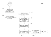
도 1a-1b는 EDE 삼중-층들을 갖는 3-차원 다중-층 세라믹 캐패시터를 발생시키기 위한 실시예에 따른 변형된 제조 프로세스를 총괄하여 예시한다.
도 1c는 도 1의 방법에 금속 코팅된 유전체 테잎이 사용될 때 제조되는 MLCC의 단면 야금학적 미세구조도를 예시한다.
도 2a는 소결 이전의 MLCC의 구성을 예시한다.
도 2b는 유전체로 구성되는 그것의 단부들에서의 절연부를 갖는 MLCC의 구성을 예시한다.
도 2c는 Ag-유전체 복합물이 전기적으로 단락되는 MLCC의 비교 예를 예시한다.
도 3은 유전체 테잎의 표면 상에 전극 및 Ag-유전체들 양자 모두가 프린팅되는 비대칭적 레이아웃을 갖는 MLCC를 예시한다.
도 4는 도 3의 예시적 실시예의 비대칭적 레이아웃에 관한 MLCC의 예비-소결 스테이지 및 대칭적 레이아웃을 예시한다.
도 5a는 유전체 층들이 아직 형성되지 않은, 소결 이전의 예시적 MLCC를 예시한다.
도 5b는 소결 이후의 예시적 MLCC의 야금학적 미세구조 단면도를 예시한다.
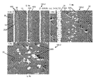
도 6a-6c는 대략 5시간 동안 대략 940C에서 MLCC를 소결한 이후에, Ag 코팅된 유전체 테잎들을 사용하는 제1 샘플의 주사 전자 현미경(SEM)에 의하여 제조되는 야금학적 미세구조 단면도들을 예시한다.
도 7a-7d는 도 6a-6c의 샘플 MLCC에 대응하는 다른 제1 샘플 MLCC들의 광학 현미경에 의하여 제조되는 야금학적 미세구조 단면도들을 예시한다.
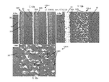
도 8a-8c는 대략 5시간 동안 대략 940C에서 MLCC를 소결한 이후에, Ag 코팅된 유전체 테잎들을 사용하는 제2 샘플의 주사 전자 현미경(SEM)에 의하여 제조되는 야금학적 미세구조 단면도들을 예시한다.
도 9a-9d는 도 8a-8c의 샘플 MLCC에 대응하는 다른 제2 샘플 MLCC의 광학 현미경에 의하여 제조되는 야금학적 미세구조 단면도들을 예시한다.
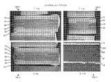
도 10a-10c는 대략 1시간 동안 대략 975C에서 MLCC를 소결한 이후에, Ag 코팅된 유전체 테잎들을 사용하는 제3 샘플 MLCC의 주사 전자 현미경(SEM)에 의하여 제조되는 야금학적 미세구조 단면도들을 예시한다.
도 11a-11c는 도 10a-10c의 샘플 MLCC에 대응하는 다른 제3 샘플 MLCC들의 광학 현미경에 의하여 제조되는 야금학적 미세구조 단면도들을 예시한다.
도 12a-12c는 대략 1시간 동안 대략 975C에서 MLCC를 소결한 이후에, Ag 코팅된 유전체 테잎들을 사용하는 제4 샘플 MLCC의 주사 전자 현미경(SEM)에 의하여 제조되는 야금학적 미세구조 단면도들을 예시한다.
도 13a-13d는 도 12a-12c의 샘플 MLCC에 대응하는 다른 제4 샘플 MLCC들의 광학 현미경에 의하여 제조되는 야금학적 미세구조 단면도들을 예시한다.
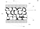
도 14는 3-차원 캐패시터의 예시적 일 실시예를 형성하는 단일 EDE 삼중-층의 단면도를 예시하며, 3-차원 구조물들이 유전체 미립자들 상에 전도성 코팅들로부터 형성된다.
도 15는 3-차원 캐패시터의 다른 예시적 실시예를 형성할 수 있는 단일 EDE 층의 단면도를 예시하며, 여기서 3-차원 구조물들은 코팅된 유전체 입자들의 유전체 슬러리로 혼합된 금속 입자들로부터 형성된다.
도 16은 3-차원 캐패시터의 다른 예시적 실시예를 형성할 수 있는 단일 EDE 삼중-층의 단면도를 예시하며, 여기서 금속 입자들은 유전체 그린 테잎으로 함침된다(impregnated into).
도 17은 3-차원 캐패시터의 다른 예시적 실시예를 형성할 수 있는 단일 EDE 삼중-층의 단면도를 예시하며, 여기서 금속 입자들은 유전체 그린 테잎으로 함침되며, 컨덕터 플레이트들은 유전체 층 근처의 낮은 용융점 전극 재료의 층을 포함한다.
도 18은 3-차원 캐패시터의 다른 예시적 실시예를 형성할 수 있는 단일 EDE 삼중-층의 단면도를 예시하며, 여기서 금속 코팅된 미립자는 전도성 층들을 생성하는데 사용되며, 상기 전도성 층들 사이에 유전체 층이 샌드위치된다.
도 19는 3-차원 캐패시터의 다른 예시적 실시예를 형성할 수 있는 단일 EDE 삼중-층의 단면도를 예시하며, 여기서 금속 코팅된 세라믹 층이 유전체 층과 전극 층들 사이에 형성된다.
도 20은 3-차원 캐패시터의 다른 예시적 실시예를 형성할 수 있는 단일 EDE 삼중-층의 단면도를 예시하며, 여기서 3-차원 구조물들이 1차 컨덕터 층들로부터 유전체 층으로 수직으로 돌출된다.
도 21은 3-차원 캐패시터의 다른 예시적 실시예를 형성할 수 있는 단일 EDE 삼중-층의 단면도를 예시하며, 여기서 3-차원 구조물들이 1차 컨덕터 층들로부터 유전체 층으로 돌출된다.
도 22는 유전체 층에 다수의 별개의 금속 함유물들을 갖지만 전극들 근처의 "공핍 층"이 없는 3-차원 캐패시터의 다른 예시적 실시예의 단면도를 예시한다.1A-1B collectively illustrate a modified manufacturing process according to an embodiment for generating a three-dimensional multi-layer ceramic capacitor having EDE triple-layers.
FIG. 1C illustrates a cross-sectional metallurgical microstructure diagram of an MLCC made when a metal coated dielectric tape is used in the method of FIG. 1.
2A illustrates the configuration of the MLCC before sintering.
2B illustrates the configuration of an MLCC with insulation at its ends composed of a dielectric.
2C illustrates a comparative example of MLCCs in which Ag-dielectric composites are electrically shorted.
3 illustrates an MLCC with an asymmetrical layout in which both electrodes and Ag-dielectrics are printed on the surface of the dielectric tape.
4 illustrates the pre-sintering stage and symmetrical layout of the MLCC with respect to the asymmetrical layout of the example embodiment of FIG. 3.
5A illustrates an example MLCC before sintering, where dielectric layers have not yet been formed.
5B illustrates a metallurgical microstructure cross-sectional view of an exemplary MLCC after sintering.
6A-6C illustrate metallurgical microstructure cross-sectional views prepared by scanning electron microscopy (SEM) of a first sample using Ag coated dielectric tapes after sintering MLCC at approximately 940C for approximately 5 hours.
7A-7D illustrate cross-sectional views of metallurgical microstructures fabricated by an optical microscope of other first sample MLCCs corresponding to the sample MLCCs of FIGS. 6A-6C.
8A-8C illustrate metallurgical microstructure cross-sectional views made by scanning electron microscopy (SEM) of a second sample using Ag coated dielectric tapes after sintering MLCC at approximately 940C for approximately 5 hours.
9A-9D illustrate metallurgical microstructure cross-sectional views produced by an optical microscope of another second sample MLCC corresponding to the sample MLCC of FIGS. 8A-8C.
10A-10C illustrate metallurgical microstructure cross-sectional views produced by scanning electron microscopy (SEM) of a third sample MLCC using Ag coated dielectric tapes after sintering the MLCC at approximately 975 C for approximately one hour. .
11A-11C illustrate cross-sectional views of metallurgical microstructures made by optical microscopy of other third sample MLCCs corresponding to the sample MLCCs of FIGS. 10A-10C.
12A-12C illustrate metallurgical microstructure cross-sectional views prepared by scanning electron microscopy (SEM) of a fourth sample MLCC using Ag coated dielectric tapes after sintering the MLCC at approximately 975 C for approximately one hour. .
13A-13D illustrate metallurgical microstructure cross-sectional views prepared by optical microscopy of other fourth sample MLCCs corresponding to the sample MLCCs of FIGS. 12A-12C.
14 illustrates a cross-sectional view of a single EDE triple-layer forming one exemplary embodiment of a three-dimensional capacitor, wherein three-dimensional structures are formed from conductive coatings on dielectric particulates.
15 illustrates a cross-sectional view of a single EDE layer that can form another exemplary embodiment of a three-dimensional capacitor, wherein the three-dimensional structures are formed from metal particles mixed into a dielectric slurry of coated dielectric particles.
FIG. 16 illustrates a cross-sectional view of a single EDE triple-layer that may form another exemplary embodiment of a three-dimensional capacitor, wherein the metal particles are impregnated into a dielectric green tape.
17 illustrates a cross-sectional view of a single EDE triple-layer that may form another exemplary embodiment of a three-dimensional capacitor, wherein the metal particles are impregnated with a dielectric green tape, and the conductor plates are low melting point electrodes near the dielectric layer. A layer of material.
FIG. 18 illustrates a cross-sectional view of a single EDE triple-layer that may form another exemplary embodiment of a three-dimensional capacitor, wherein metal coated particulates are used to create conductive layers, with a dielectric layer between the conductive layers. This is a sandwich.
19 illustrates a cross-sectional view of a single EDE triple-layer that may form another exemplary embodiment of a three-dimensional capacitor, wherein a metal coated ceramic layer is formed between the dielectric layer and the electrode layers.
20 illustrates a cross-sectional view of a single EDE triple-layer that may form another exemplary embodiment of a three-dimensional capacitor, wherein the three-dimensional structures project vertically from the primary conductor layers to the dielectric layer.
21 illustrates a cross-sectional view of a single EDE triple-layer that may form another exemplary embodiment of a three-dimensional capacitor, wherein the three-dimensional structures protrude from the primary conductor layers to the dielectric layer.
22 illustrates a cross-sectional view of another exemplary embodiment of a three-dimensional capacitor having a plurality of distinct metal inclusions in the dielectric layer but without a “depletion layer” near the electrodes.
이전에 개시된 실시예들 뿐 아니라, 실시예들의 피쳐들 및 양상들은 캐패시턴스 효율을 향상시키기 위한 캐패시터 및 제조 방법들을 제공하는 것에 관련된다. 더욱 구체적으로, 향상된 캐패시터는 유전체와의 계면의 포인트에서 3-차원 양상들을 갖는 전극 층들로 구성될 수 있다. 바람직하게, 3-차원 캐패시터의 실시예들은 본 기술분야의 당업자에게 알려진 현재 캐패시터 설계들과 비교할 때, 캐패시터를 수용하기 위하여 회로에 요구되는 공간 풋프린트(space footprint)를 대폭 감소시킨다. 증가된 용량성 밀도는 하이 k(높은 상수) 유전체 재료들, 계속해서 증가하는 적층물의 부가적인 "전극-유전체-전극" 배열들, 또는 다수의 캐패시터들을 함께 직렬로 잇는(stringing) 것을 필수적으로 요구하지 않고 구현될 수 있다.In addition to the previously disclosed embodiments, features and aspects of the embodiments relate to providing capacitors and fabrication methods for improving capacitance efficiency. More specifically, the improved capacitor may be composed of electrode layers having three-dimensional aspects at the point of interface with the dielectric. Advantageously, embodiments of three-dimensional capacitors significantly reduce the space footprint required for a circuit to accommodate a capacitor as compared to current capacitor designs known to those skilled in the art. Increased capacitive density necessarily requires high k (high constant) dielectric materials, additional "electrode-dielectric-electrode" arrangements of ever-increasing stacks, or stringing multiple capacitors together. Can be implemented without
몇몇 실시예들에서, 하나 또는 그 초과의 금속화된 유전체 층들을 포함하는, MLCC와 같은 캐패시터가 개시되며, 유전체 층들 각각은 전압 단자들에 커플링하도록 적응되는 2개의 전극들 사이에 배치된다. 통합된 금속은 퍼컬레이션 네트워크를 형성하지 않는 개별적인 금속성 함유물들을 형성하는 것을 보장하면서, 유전체 층 내에 상당량의 금속이 포함될 수 있는 것이 발견되었다. 사실상, 몇몇 경우들에서, 통합된 금속의 체적 분율은 퍼컬레이션의 발생을 초래하지 않고 퍼컬레이션 임계치를 초과할 수 있다. 예를 들어, 몇몇 실시예들에서, 유전체 층의 금속의 체적 분율은 적어도 약 40%일 수 있다. 게다가, 몇몇 실시예들에서, 공핍 유전체 층(즉, 실질적으로, 그리고 바람직하게는 완전히 금속이 없는 유전체 층)은 적어도 하나의 그리고 바람직하게는 금속화된 층이 그 사이에 배치되는 2개 전극들 모두로부터 금속화된 유전체 층을 분리한다. 이러한 방식으로, 높은 캐패시턴스 뿐 아니라 높은 용량성 밀도들을 나타내는 캐패시터들이 달성될 수 있다.In some embodiments, a capacitor, such as an MLCC, is disclosed that includes one or more metallized dielectric layers, each of which is disposed between two electrodes adapted to couple to voltage terminals. It has been found that the integrated metal can contain significant amounts of metal in the dielectric layer, ensuring that it forms individual metallic inclusions that do not form a percolation network. Indeed, in some cases, the volume fraction of the integrated metal may exceed the percalation threshold without causing the occurrence of percalation. For example, in some embodiments, the volume fraction of metal of the dielectric layer can be at least about 40%. In addition, in some embodiments, a depletion dielectric layer (ie, a substantially and preferably completely metal free dielectric layer) may comprise two electrodes with at least one and preferably metallized layer disposed therebetween. Separate the metallized dielectric layer from all of them. In this way, capacitors exhibiting high capacitance as well as high capacitive densities can be achieved.
세라믹 기반 캐패시터들의 문맥에서 MLCC들의 예시적인 실시예들이 개시되나, 본 기술분야의 당업자는 MLCC의 다양한 실시예들이 세라믹 기반 컴포넌트들을 반드시 포함하지는 않을 수 있으며, 이로써, 본 개시물의 범위가 세라믹 기반 실시예들로 제한되지 않을 것임을 이해할 것이다. 또한, 개시된 실시예들의 유전체, 애노드 및 캐소드 층들은 가끔은 일반적으로 "플레이트들" 또는 "층들"로서 지칭될 수 있다. 그러나 본 개시물은 전도성 또는 유전체 층들이 3-차원 캐패시터의 모든 실시예들에서 "강성(rigid)" 또는 "스티프(stiff)" 플레이트들이어야 하도록 해석되지 않을 것이다. 그보다는, 특정 예시적 실시예가 전달되는 문맥에서 취해지는 바와 같은 용어 "플레이트는 잉크들, 페이스트, 변형가능한 몸체들의 메카닉들 등 등의 적용으로부터 생성되는 플레이트들 또는 강성 플레이트들을 포함하는 임의의 컴포넌트 층 또는 그것의 생성 방법을 포함하는 것으로 이해될 것이다. 즉, 용어 "플레이트"는 단순히 3-차원 캐패시터 내에 특정 층을 지칭하는 것으로 이해될 것이며, 그러한 층은 그것이 연관되는 예시적인 실시예들의 개시내용에 관하여 설명될 수 있는 양상들 및 피쳐들에 의해서만 제한된다.Exemplary embodiments of MLCCs are disclosed in the context of ceramic based capacitors, but those skilled in the art will recognize that various embodiments of MLCC may not necessarily include ceramic based components, such that the scope of the present disclosure is a ceramic based embodiment. It will be understood that this will not be limited. In addition, the dielectric, anode and cathode layers of the disclosed embodiments may sometimes be referred to generally as "plates" or "layers." However, this disclosure will not be construed so that the conductive or dielectric layers should be "rigid" or "stiff" plates in all embodiments of a three-dimensional capacitor. Rather, the term " plate as taken in the context of which certain exemplary embodiments are delivered is any component layer comprising plates or rigid plates resulting from the application of inks, pastes, mechanics of deformable bodies, and the like. Or a method of its creation, ie, the term “plate” will be understood to simply refer to a particular layer within a three-dimensional capacitor, which layer is to be described in the disclosure of the exemplary embodiments with which it is associated. It is limited only by the aspects and features that may be described in terms of.
일반적으로, 본 발명의 개시물에 설명되는 특정 실시예들은 단지 예시적 목적들을 위해 공급되며, MLCC의 범위를 제한하는 것으로 해석되지 않을 것이다. 또한, MLCC의 다양한 실시예들이 상이한 컴포넌트 또는 재료 선택들을 이용할 수 있으나, 본 개시물의 예시적인 실시예들에 관하여 설명되는 예시적인 재료들은 MLCC 내에 포함될 수 있는 재료들 또는 컴포넌트들의 포괄적 리스팅으로서 의도되지 않는다. MLCC들을 생성하는데 사용되는 재료들, 그리고 특히 애노드 층, 캐소드 층, 단자들, 전도성 돌출부들, 유전체 또는 "그린 테잎" 층과 같은 캐패시터들의 피쳐들은 (예를 들어, 캐패시터가 의도되는 특정 애플리케이션들에 기반하여) 일 실시예로부터 다른 실시예로 변경될 수 있으며, 혹시 특정 실시예의 신규한 피쳐 또는 양상을 발생시키는 역할을 하더라도, 개시물의 범위를 제한하지 않을 것이다.In general, the specific embodiments described in the present disclosure are provided for illustrative purposes only and shall not be construed as limiting the scope of the MLCC. In addition, although various embodiments of the MLCC may use different component or material selections, the example materials described with respect to the example embodiments of the present disclosure are not intended as a comprehensive listing of materials or components that may be included within the MLCC. . The materials used to create the MLCCs, and in particular the features of the capacitors, such as anode layer, cathode layer, terminals, conductive protrusions, dielectric or "green tape" layer, may be used (e.g., in particular applications where the capacitor is intended). Change from one embodiment to another, and will not limit the scope of the disclosure, even if it serves to generate new features or aspects of a particular embodiment.
주어진 3-차원 캐패시터의 다양한 컴포넌트들 또는 피쳐들에 대한 재료 선택들은 다음을 포함한다(그러나 이에 제한되는 것은 아님): 전극들에 대해 - 은(예를 들어, 약 100 중량%), 은 팔라듐 합금(예컨대, 약 95 중량% Ag 내지 약 5 중량% 팔라듐), 팔라듐, 및 금, 백금, 이리듐, 및 그들의 합금들과 같은(그러나 이에 제한되는 것은 아님) 다른 귀금속들뿐 아니라, 텅스텐, 몰리브덴, 탄탈룸, 니오븀, 하프늄 및 레늄과 같은(그러나 이에 제한되는 것은 아님) 내화 금속들 및 니켈, 니켈 합금, 구리 및 구리 합금들과 같은(그러나 이에 제한되는 것은 아님) 비금속(base metal)들; 유전체 층에 대해 - 세라믹 및 유리-세라믹, 은-코팅된 세라믹들, 팔라듐-코팅된 세라믹들, 은 팔라듐-코팅된 세라믹들과 같은(그러나 이에 제한되는 것은 아님) 귀금속 코팅된 세라믹들 등뿐 아니라, 은 코팅된 포뮬레이팅된 티탄산 바륨 기반 유전체들, 은 코팅된 유리 비드들, 및 알루미나 및 탄탈룸 산화물과 같은(그러나 이에 제한되는 것은 아님) 무기 산화물들.Material selections for the various components or features of a given three-dimensional capacitor include, but are not limited to: silver (for example, about 100% by weight), silver palladium alloy, relative to the electrodes Tungsten, molybdenum, tantalum, as well as palladium, and other precious metals such as, but not limited to, gold, platinum, iridium, and their alloys (eg, about 95% Ag to about 5% Palladium) Refractory metals such as, but not limited to, niobium, hafnium and rhenium, and base metals such as, but not limited to nickel, nickel alloys, copper and copper alloys; For dielectric layers-as well as noble metal coated ceramics such as, but not limited to, ceramic and glass-ceramic, silver-coated ceramics, palladium-coated ceramics, silver palladium-coated ceramics, and the like. Silver coated formulated barium titanate based dielectrics, silver coated glass beads, and inorganic oxides such as, but not limited to, alumina and tantalum oxide.
이제 도면들로 돌아가, 예시적인 3-차원 캐패시터들 및 제조 방법들의 다양한 양상들, 피쳐들 및 실시예들이 더욱 상세히 제시될 것이며, 도면들에서 동일한 참조 번호들은 도면들 전반에 걸쳐 동일한 엘리먼트들을 나타낸다. 도면들 및 상세한 설명에서 진술되는 바와 같은 예들은 설명으로서 제공되며, MLCC, 그리고 특히 3-차원 캐패시터의 범위에 대한 제한들로서 의도되지 않는다.Turning now to the drawings, various aspects, features, and embodiments of exemplary three-dimensional capacitors and fabrication methods will be presented in more detail, wherein like reference numerals refer to like elements throughout the figures. Examples as set forth in the figures and the detailed description are provided by way of explanation and are not intended as limitations on the scope of MLCCs, and in particular three-dimensional capacitors.
3-차원 캐패시터 또는 3-차원 캐패시터 내에 포함될 수 있는 구성의 특정 재료들을 제조하기 위한 방법들이 설명된다. 따라서 3-차원 캐패시터와 같은 MLCC는 본 기술분야의 당업자에게 이해되는 바와 같이 첨부된 청구항들 및 그들의 동등물들의 범위 내에 있는 다음의 예들에 대한 임의의 변경들 및 변형들을 포함한다.Methods for manufacturing certain materials of construction that can be included in a three-dimensional capacitor or a three-dimensional capacitor are described. Thus, an MLCC, such as a three-dimensional capacitor, includes any modifications and variations to the following examples that are within the scope of the appended claims and their equivalents as would be understood by those skilled in the art.
MLCC의 예시적인 실시예들에 따라, 유전체 층의 코팅되지 않은 세라믹 입자들 대신에 금속 코팅된 세라믹 입자들 또는 은 유전체 복합물을 사용함으로써, 3-차원 캐패시터 실시예와 같은 MLCC들을 생성하는데 사용될 수 있는 변형된 제조 프로세스가 설명된다. 코팅된 유전체 재료들 또는 금속-유전체 복합물들 또는 혼합물들은 MLCC를 렌더링(render)하기 위한 향상된 제조 방법과 통합될 수 있다.In accordance with exemplary embodiments of MLCCs, the use of metal coated ceramic particles or silver dielectric composites in place of the uncoated ceramic particles of the dielectric layer can be used to produce MLCCs such as three-dimensional capacitor embodiments. Modified manufacturing processes are described. Coated dielectric materials or metal-dielectric composites or mixtures can be integrated with an improved manufacturing method for rendering an MLCC.
3-차원 캐패시터의 몇몇 실시예들은 다중-층 세라믹 캐패시터들 (MLCC) 등을 포함하며, 따라서 본 개시물에 설명되고 도시되는 3-차원 캐패시터의 실시예들 중 다수가 MLCC 내의 단일 삼중-층을 나타낼 수 있는 단일 "전극-유전체-전극" 배열(EDE)만을 나타내도록 의도된다는 것이 이해될 것이다.Some embodiments of three-dimensional capacitors include multi-layer ceramic capacitors (MLCC), and the like, so that many of the embodiments of three-dimensional capacitors described and shown in this disclosure may employ a single triple-layer in an MLCC. It will be understood that it is intended to represent only a single "electrode-dielectric-electrode" arrangement (EDE) that can be represented.
도 1-2는 발명의 예시적 실시예에 따른 EDE 삼중-층들을 갖는 MLCC를 발생시키는데 사용될 수 있는 하나의 예시적 제조 방법(101)을 총괄하여 예시한다. 도 1을 참고하여, MLCC에 대한 제조 프로세스에서, 세라믹 파우더(205)는, 세라믹 슬러리(210)를 형성하기 위하여 용매, 폴리머 수지 및 첨가물들, 예컨대 분산제를 포함할 수 있는 화합물과 같은 캐리어로 혼합된다(단계(105)).1-2 collectively illustrate one
세라믹 슬러리(210)는 프로세스의 테잎 주조 단계(11)에서 "그린 세라믹 테잎"(215)을 주조하는데 사용된다. 세라믹 파우더 슬러리로부터 만들어진 그린 테잎(215)은 결국 캐패시터의 유전체 층으로서 기능할 것이다. 예시적인 그린 테잎은 세라믹 슬러리로부터 형성되는 것으로서 상기 설명되나, 발명의 실시예들이 포뮬레이팅된 티탄산 바륨 기반 유전체들과 같은(그러나 이에 제한되는 것은 아님) 세라믹들, 저온 동시 소성(low-temperature co-fired) 세라믹들에서 사용되는 Ca-B-Si-0 시스템 유리 세라믹들과 같은(그러나 이에 제한되는 것은 아님) 유리 세라믹들, 및 고온 동시 소성 세라믹들과 다양한 금속 코팅된 세라믹들 및 무기 산화물들 및 화합물들에서 사용되는 알루미나 유리 세라믹들을 제외한, 또는 그것에 부가한 재료들로 만들어진 그린 테잎 컴포넌트들을 포함할 수 있다는 것이 이해될 것이다. 코팅 또는 혼합을 위해 사용되는 금속은, 은-팔라듐 합금들(약 95 중량% Ag 및 약 5 중량%Pd, 더욱 바람직하게는 약 90 중량%Ag 및 약 10 중량%Pd 그리고 가장 바람직하게는 약 70 중량%Ag 및 약 30 중량%Pd 범위의 은 팔라듐의 중량 퍼센트 조성물과 같은) 뿐 아니라, 팔라듐, 팔라듐 합금들, 백금, 백금 합금들, 은, 은 합금들, 금, 금 합금들 및 다른 귀금속들 및 그들의 개별적인 합금들, 예컨대, 이리듐, 로듐, 루테늄뿐 아니라, 구리, 니켈, 철, 코발트, 망간, 티타늄, 아연, 및 내화 금속들, 예컨대(그러나 이에 제한되는 것은 아님) 텅스텐, 몰리브덴, 지르코늄, 탄탈룸, 및 니오븀을 포함할 수 있다(그러나 이에 제한되는 것은 아님).Ceramic slurry 210 is used to cast “green ceramic tape” 215 in the tape casting step 11 of the process. The green tape 215 made from the ceramic powder slurry will eventually function as the dielectric layer of the capacitor. Exemplary green tapes are described above as being formed from ceramic slurries, but embodiments of the invention include ceramics such as, but not limited to, formulated barium titanate based, low-temperature co- fired) glass ceramics, such as, but not limited to, Ca-B-Si-0 system glass ceramics used in ceramics, and high temperature co-fired ceramics and various metal coated ceramics and inorganic oxides, and It will be appreciated that it may include green tape components made of materials other than or in addition to the alumina glass ceramics used in the compounds. The metal used for coating or mixing may comprise silver-palladium alloys (about 95 weight percent Ag and about 5 weight percent Pd, more preferably about 90 weight percent Ag and about 10 weight percent Pd and most preferably about 70 Palladium, palladium alloys, platinum, platinum alloys, silver, silver alloys, gold, gold alloys and other precious metals, as well as palladium, palladium alloys, platinum, platinum alloys, such as And their individual alloys such as iridium, rhodium, ruthenium, as well as copper, nickel, iron, cobalt, manganese, titanium, zinc, and refractory metals such as, but not limited to, tungsten, molybdenum, zirconium, Tantalum, and niobium, but are not limited thereto.
그린 테잎의 표면 텍스쳐링은 또한 기계적 롤러를 사용하여 만들어질 수 있다. 예를 들어, 그린 테잎의 상단 상의 롤링 이후에, 롤러 상의 텍스쳐는 그린 테잎 위로 전사될 수 있다. 추후에, 일단 주조되면, 그린 테잎(215)은 예시적인 프로세스에서 단계(120)에서 스크린 프린팅되도록 진행된다.Surface texturing of the green tape can also be made using mechanical rollers. For example, after rolling on the top of the green tape, the texture on the roller can be transferred onto the green tape. Later, once cast, green tape 215 proceeds to screen printing in
단계(120)에서 스크린 프린팅 이전에, 전극 금속 파우더(220)는 캐리어 화합물과 혼합되어(단계(115)) 전극 잉크(225)를 형성한다. 전극 잉크(225)는 단계(120)에서 세라믹 그린 테잎(215) 위에 스크린 프린팅되어, 최종적 MLCC의 단일 유전체-전도체 이중층을 형성한다.Prior to screen printing in
단계(120)는 도 1c-13과 함께 하기에 설명되는 바와 같은 이 발명의 시스템 및 방법의 하나의 주요 양상이다. 은 유전체 복합물 또는 혼합물은 본 기술분야의 당업자에게 알려진 "그린 테잎 스테이지"로서 또한 지칭되는, 이 스크린 프린팅 단계(120)에서 사용될 수 있다. 본 기술분야의 당업자에 의해 이해되는 바와 같이, 은 유전체 복합물은 금속(예를 들어, 은) 코팅된 유전체 테잎, 금속(예를 들어, 은) 파우더와 혼합된 유전체, 금속(예를 들어, 은) 코팅된 세라믹 입자들, 또는 금속 유전체 복합물을 형성하기 위한 임의의 다른 방식들을 포함할 수 있다. 금속-코팅된 세라믹 입자들이 이용되는 몇몇 실시예들에서, 세라믹 입자들은 약 0.01 미크론 내지 약 10.0 미크론 범위의 사이즈를 갖는다.Step 120 is one major aspect of the systems and methods of the present invention as described below in conjunction with FIGS. 1C-13. Silver dielectric composites or mixtures may be used in this
금속(즉, 은) 파우더 또는 금속(즉, 은) 코팅된 유전체 테잎들과 혼합되는 유전체 입자들을 포함하는 유전체 복합물이, 상기 단계(120)에서 설명된 예시적인 코팅되지 않은 세라믹 파우더(205) 대신에 사용된다면, 도 14-22, 또는 도 1c-13에 예시되는 MLCC들이 형성될 수 있다. 예를 들어, 몇몇 실시예들에서, 은-코팅된 세라믹 입자들이 이용될 수 있다. 하기에 더욱 상세히 논의되는 바와 같이, 은 코팅된 세라믹 입자들에 대하여 약 850℃ 내지 약 950℃ 범위의 소결 온도와 같이 특정 프로세싱 파라미터들이 이용될 때, 금속의 일부분이 전극들 중 적어도 하나의 전극에 근접한 구역(region)으로부터 그 전극으로 이동하고, 그에 의해 공핍 층(즉, 실질적으로 금속이 없는 층)을 그 전극 근처에 발생시킨다. 몇몇 경우들에서, 전극으로 이동한 금속은 예를 들어, 핑거-형 돌출부들의 형태로 그 전극의 표면 층에서의 증가를 야기하며, 이는 결국 후속 프로세싱 단계들을 통해 형성될 캐패시터의 캐패시턴스를 향상시킬 수 있다. 몇몇 실시예들에서, 전극은, 공핍 층을 발생시키도록, 전극 근처의 얇은 복합물 금속-유전체 층에서의 그 전극으로의 금속의 이동을 용이하게 하기 위하여 유전체 내에 포함되는 금속과 공동으로 적어도 하나의 금속 성분을 갖는다.Dielectric composites comprising metal (i.e. silver) powder or dielectric particles mixed with metal (i.e. silver) coated dielectric tapes are used instead of the exemplary uncoated ceramic powder 205 described in
단계들(105 내지 120)이 반복됨에 따라, 다수의 스크린 프린팅된 그린 테잎 시트들(230)(각각의 시트는 단일 유전체-전도체 이중층을 포함함)이 단계(125)에서 적층되어, EDE 삼중-층들이 후속 시트의 그린 테잎의 하단 표면과의 스크린 프린팅된 전도성 층의 반복된 병치(juxtaposition)를 통하여 생성된다. 단계(125)로부터 초래되는 적층물은 라미네이션 프로세스에서의 단계(130)에서 함께 라미네이팅된다. 결과적인 라미네이팅된 적층물(235)은 그 후 단계(135)에서 다수의 인터리빙된 EDE 삼중-층들을 포함하는 개별적인 세라믹 그린 칩들(240)로 변환된다.As steps 105-120 are repeated, a number of screen printed green tape sheets 230 (each sheet comprising a single dielectric-conductor bilayer) are stacked in
도 1b에서, 방법 또는 방법(101)은 단계(140)에서 개별적인 세라믹 그린 칩들(240)이 소성 프로세스에 노출되는 것을 계속한다. 소성 프로세스에서(단계(140)), 그린 세라믹 칩들(240)은 상기 언급된 슬러리들의 무기물들이 제거되게 하기 위하여 벨트 퍼니스(belt furnace) 등을 통해 전송되고, 그에 의해 EDE 삼중-층들을 포함하는 세라믹 캐패시터 칩(245)으로 그린 세라믹 칩(240)을 소결할 수 있다. 소결 온도는 예를 들어, 유전체-전도체 층을 형성하기 위하여 사용되는 금속에 기반하여 선택될 수 있다. 일반적으로, 소결 온도는 금속의 적어도 부분적인 용융을 야기하기에 충분히 높다. 예로서, 소결 온도는 비금속 MLCC에서 은 코팅된 세라믹들에 대해 약 750℃ 내지 약 980℃ 범위일 수 있는 한편, 니켈 코팅된 세라믹에 대해 약 1100℃ 내지 약 1500℃일 수 있다.In FIG. 1B, the method or
단계(150)에서, 소결된 세라믹 캐패시터 칩(245)은 그 후 전도성 금속 파우더(255)로부터 혼합된(단계(145)) 터미네이션 잉크(termination ink)(250)로의 디핑(dipping)을 통해 2개 단부들 각각에서 금속화될 수 있다. 터미네이션 금속화(termination metallization)는 회로 보드 애플리케이션에 대한 전기 콘택 포인트들 뿐 아니라 교번하는(alternating) 전도성 플레이트들 사이에 내부 접속부를 제공한다. 터미네이팅된(terminated) 칩들(260)은 그 후 건조되고 터미네이션 소성 프로세스에서 단계(155)에서 다시 소성되어, MLCC(265)가 된다. 몇몇 실시예들에서, 소성 온도는 예를 들어, 약 750℃ 내지 약 900℃의 범위일 수 있다. 마지막으로, 단계(160)에서, 주석 도금이 도금 프로세스에서 MLCC들(265)에 적용될 수 있어, 터미네이션 금속화를 보호하고, 납땜 연결들의 용이성을 제공한다. 제조 분야의 당업자에게 알려진 바와 같이, MLCC들(265)은 그 후 회로의 이용 이전에 품질 제어를 위한 단계(165)에서 테스팅 프로세스를 겪을 수 있다(단계(170)).In
도 1c-13의 3-D 캐패시터들을 구성하기 위한 고유 컴포넌트 선택과 결합된 변형된 제조 프로세스: 프린팅된 코팅들을 갖는 금속 코팅된 유전체 테잎들 또는 슬러리들Modified manufacturing process combined with unique component selection to construct the 3-D capacitors of FIGS. 1C-13: metal coated dielectric tapes or slurries with printed coatings
금속 코팅된 유전체 테잎들을 사용하는 실제 샘플의 소결 후 도면: 도 1c Post-sintering drawing of a real sample using metal coated dielectric tapes: FIG. 1C
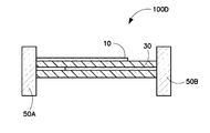
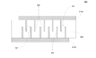
이제 도 1c를 참고하여, 이 도면은 도 1a-1b의 방법에서 은 코팅된 유전체 테잎(30)이 사용될 때 생성되는 MLCC(100A)의 단면도를 예시한다. 이 도면은 대략 1000배의 확대 레벨로 주사 전자 현미경을 사용하여 생성된다. MLCC(100A)는 수 개의 층들을 포함한다: 금속 전극 층(10), 유전체 층(20A)(본 명세서에서 공핍 층(20A)으로도 지칭됨), 금속-유전체 테잎 층(30)(본 명세서에서 금속화된 유전체 층(30)으로도 지칭됨) 및 유전체 층(40). 몇몇 실시예들에서, 유전체 층(40)은 공핍 층(20A)의 두께보다 큰, 예를 들어, 이 예에서는 약 6배만큼 큰 두께를 가질 수 있다. 소결 동안에 이동하는 금속의 포켓들 또는 함유물들(605)이 또한 가시적이다. 여기서 유전체 층(20A)은 은-유전체 층(30) 외부로의 은 이동으로부터 인-시튜로 형성된다는 것이 유념된다.Referring now to FIG. 1C, this figure illustrates a cross-sectional view of the
다음은 이 MLCC 구조물(100)을 형성하는데 사용되는 예시적인 재료들이다. 전극 층(10)은 95/5 Ag/Pd(대략 5% 팔라듐을 갖는 대략 95% 은)를 포함한다. 유전체 층(40)은, MRA Laboratories에 의해 제조되는 VLF-220Aq3라는 제품명 하의 상업적으로 이용가능한 물건으로서 팔리는, 저온 소성가능 COG 타입 티탄산염 유전체를 포함할 수 있으며, 금속-유전체(즉, Ag-유전체) 복합물 테잎 층(30)은 VLF-220Aq3의 대략 30%(중량%)의 은 코팅을 포함할 수 있다. 소결 온도는 약 940 ℃ 내지 약 975 ℃의 범위일 수 있다. 캐패시터 칩들의 사이즈는 2018(대략 0.20 인치 × 대략 0.18 인치)과 유사한 사이즈들을 포함할 수 있다. 통상적으로, 6개의 활성 층들이 캐패시터 칩들을 제조하는데 사용된다. 통상적인 유전체 층 두께는 약 0.001 인치(약 25 미크론)이다. 다른 사이즈들이 발명의 범위 내에 포함될 수 있다.The following are exemplary materials used to form this MLCC structure 100.
이제 도 1c(소결 이후에 전자 현미경에 의해 생성된 단면도임)를 참고하여, 캐패시터(100A)는 Ag-유전체 복합물 테잎(30)의 상단 상에 Ag/Pd 전극(10)을 프린팅함으로써 구성될 수 있으며, Ag-유전체 복합물 테잎(30)은 유전체 층(40)에 의하여 절연된다. 유전체 층(40)은 약 30 미크론의 두께를 가질 수 있다; 반면에 Ag-유전체 복합물 테잎(30)은 소결 이후에 약 10 미크론의 두께를 갖는다.Referring now to FIG. 1C (which is a cross-sectional view generated by an electron microscope after sintering),
도 1c의 주사 전자 현미경 이미지에서, 더 밝게 음영처리된 재료들은 금속인데, 전극(10)에서 Ag/Pd이고, Ag-유전체 복합물 층(30)에서 Ag이다. 어두운 배경 음영처리 영역들은 유전체를 포함한다. Ag-유전체 복합물 내의 은의 전극(10)으로의 이동에 의하여 소결 프로세스 동안에 형성되는, 약 5 미크론의 두께를 갖는 유전체 층(20A)이 Ag/Pd 전극(10)과 나머지 Ag-유전체 복합물 층(30) 사이에 명확히 보여질 수 있다. Ag-유전체 복합물 테잎(30) 내에, 금속의 함유물들 또는 포켓들(605)이 관찰된다. 단지 순수한 유전체 테잎들만을 가지고 그리고 유전체 내의 금속의 포함 없이 만들어진 재료들 및 동일한 치수들을 갖는 제어 캐패시터의 캐패시턴스에 대해 캐패시터(100A)의 캐패시턴스를 비교할 때, 약 5배(500%)의 대략적 증가가 관찰된다.In the scanning electron microscopy image of FIG. 1C, the lighter shaded materials are metal, Ag / Pd at
예비-소결 도면들: 금속 코팅된 유전체 테잎들을 사용하는 예시적인 층 설계 - 도 2a-5aPre-sinter Drawings: Exemplary Layer Design Using Metal Coated Dielectric Tapes-FIGS. 2A-5A
이제 도 2a를 참고하여, 이 도면은 어떠한 유전체 층(40)도 없이 Ag-유전체 복합물 테잎(30)만을 사용하여 형성될 수 있는 다른 예시적인 캐패시터 구조물(100B)을 도시한다. 구체적으로, 도 2a는 소결 이전의 MLCC(100B)의 구성을 예시한다. 도 2a는 소결(도 1a의 단계들(130-135)) 이전의 그린 스테이지에서의 캐패시터(100B)의 구성을 도시한다. 도 2a에서, Ag/Pd 전극(10)은 Ag-유전체 복합물 테잎(30) 위에 직접 프린팅된다. Ag-유전체 복합물 테잎(30)은 종단(termination)(50A)에 관하여 그것의 단부들 중 하나의 단부에서 전기적으로 절연된다. 종단들(50A, 50B)은 은을 포함하는(그러나 이에 제한되는 것은 아님) 재료들로 만들어질 수 있다.Referring now to FIG. 2A, this figure illustrates another
Ag-유전체 복합물 테잎(30)의 단부들 중 하나의 단부에서의 절연체는 유전체(40) 또는 퓨지티브(fujitive) 잉크들에 의하여 형성되는 공기-충진된 캐비티(예시되지 않음)를 포함할 수 있다. 절연체는 또한 도 2b에 예시된 바와 같이 소결 동안 Ag/Pd 전극(10B)을 사용하여 형성될 수 있다. 다시 말해, 도 2b는 Ag-유전체 복합물 테잎(30)을 포함하는 그것의 단부들에서 절연체를 갖는 MLCC(100C)의 구성을 예시한다.The insulator at one of the ends of the Ag-dielectric
도 1c와 함께 설명되는 유전체 층들(20a)은 이 중간 스테이지 또는 방법의 위상에서 예시된 바와 같이 도 2b의 이 스테이지에서 아직 형성되지 않았다. 소결 시, Ag-유전체 복합물 테잎(30) 내의 은은 이동하고, 유전체 복합물 테잎(30) 내에서 인-시튜로 (도 1c에 도시된) 유전체 층(20A)을 형성한다. 도 1a에 도시된 바와 같이 소결 동안 형성되는 유전체 층(20A)과 함께, 전극 층(10) 및 Ag-유전체 복합물 테잎(30)은 도 2b의 캐패시터 구조물(100C)을 형성할 수 있다. 2개의 유전체 층들(20a)(이러한 도 2b에 미도시됨)이 각각의 Ag-유전체 복합물 테잎(30)에 형성될 수 있다는 것을 유념하라.Dielectric layers 20a described in conjunction with FIG. 1C have not yet been formed at this stage of FIG. 2B as illustrated in this intermediate stage or phase of the method. Upon sintering, the silver in the Ag-dielectric
도 2c는 Ag-유전체 복합물(30)이 전기적으로 단락되는 MLCC(100D)의 비교 예를 예시한다. 구체적으로, 도 2c는, 종단(50A) 부근의 Ag-유전체 복합물 테잎(30)의 한 단부에서 유전성 절연체(40) 또는 캐비티가 사용되지 않을 때, 모든 Ag-유전체 복합물 층(30)이 도 2a 및 2b의 실시예들에 관하여 전기적으로 단락되는, 캐패시터 구조물(100D)을 도시한다. 그러나 종단들(50)이 부가될 때 터미네이션 프로세스 동안 은 이동이 효율적으로 발생하도록 허용되거나 촉진되는 경우, Ag-유전체 층(30)을 통상적으로 통과하는 전기 전류들의 단락이 방지될 수 있다. 도 2c의 이 예시적 실시예는 또한 (도 1에 예시된 바와 같은) 유전체 층들(20a)이 아직 형성되지 않았음을 의미하는 예비-소결 스테이지를 예시한다.2C illustrates a comparative example of
페이스트는 Ag-유전체 복합물 테잎(30) 대신에 Ag-유전체 복합물 층(30)을 형성하는데 사용될 수 있다. Ag-유전체 복합물 층(30)은, 대개 은 이동이 캐패시터 구조물(100)에 대한 소결 스테이지 동안 발생한 이후, 은-유전체 층이 층(30) 내에 전극을 형성하기에 충분한 금속 재료를 갖는 것을 보장하기에 충분히 두꺼워야 한다. 도 2c의 이 실시예에 대한 Ag-유전체 복합물 층(30)의 통상적 두께는 일반적으로 도 1c의 설명에서 진술된 바와 같이 약 10 미크론의 크기들을 포함한다.The paste may be used to form the Ag-dielectric
인-시튜로 형성되는 유전체 층 두께는 프린팅된 층 두께에 의해서만 영향을 받는(affect) 것이 아니라 다른 인자들, 예컨대, 소결 온도 및 유전체의 케미스트리, 그리고 금속-유전체 복합물을 형성하는데 사용되는 금속의 성질에 의해 또한 영향을 받는다는 것이 본 기술분야의 당업자에 의하여 이해된다. 여기서 주어지는 두께는 제한 인자로서 사용되어서는 안되며, 더 얇은 인-시튜로 형성된 유전체 층이 일반적으로 더 높거나 증가된 캐패시턴스 성능을 초래한다는 것이 또한 이해된다.The dielectric layer thickness formed in-situ is not only affected by the printed layer thickness, but also other factors such as the sintering temperature and chemistry of the dielectric, and the nature of the metal used to form the metal-dielectric composite. It is understood by those skilled in the art that it is also affected by. The thickness given here should not be used as a limiting factor, and it is also understood that dielectric layers formed with thinner in-situ generally result in higher or increased capacitance performance.
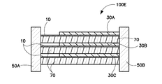
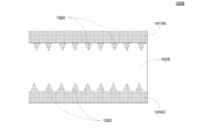
도 3은 전극(10) 및 Ag-유전체들(30) 양자 모두가 유전체 테잎(70)의 표면 상에 프린팅되는 비대칭적 레이아웃을 갖는 MLCC(100E)를 예시한다. 구체적으로, 도 3은 캐패시터 구조물(100E)의 다른 예시적 실시예를 예시하며, 여기서 전극(10) 및 3개의 Ag-유전체 층들(30A, 30B 및 30C) 모두는 유전체 테잎(70)의 상단 상에 프린팅된다. 이 구성에서, 상이한 유전체 층 두께들을 갖는 서브-캐패시터 구조들의 2개 타입들이 형성될 수 있다.3 illustrates an
도 3은 소결 이전에 그린 스테이지에서의 캐패시터 구성을 보여주며, 따라서 도 1에 도시된 바와 같이 소결 동안 형성되는 유전체 층(20A)은 아직 형성되지 않았다. 소결 이후 Ag/Pd 전극(10)과 근처에 프린팅된 제1 Ag-유전체 복합물(30A) 사이에 하나의 서브-캐패시터 구조물이 형성된다. 여기서 나머지 Ag-유전체(30A)는 하나의 전극이고, Ag/Pd(10)는 다른 전극이고, 이와 함께 유전체 층(20A)(미도시)이 얇은 캐패시터 구조물을 형성하기 위하여 유전체 공핍 층으로서 인-시튜로 형성된다. 유전체 테잎 층(70)에 걸쳐 Ag/Pd 전극(10)과 제2 프린팅된 Ag-유전체 복합물(30B) 사이에 소결 이후 다른 캐패시터 구조물이 형성된다. 제1 캐패시터 서브-구조물이 종래의 구조물인 제2 타입보다, 인-시튜로 형성되는 유전체의 더욱 얇은 층으로 인하여 훨씬 더 높은 캐패시턴스를 갖는다는 것이 명백하다.3 shows the capacitor configuration at the green stage prior to sintering, so that the
프린팅된 제1, 제2 및 제3 Ag-유전체 복합물들(30A, 30B, 30C)은 이들 재료들이 그들 자신의 개별적인 컴포넌트 제조 동안 형성된다는 점에서 도 2c의 실시예의 Ag-유전체 복합물 테잎(30)과 상이하다. 도 2a, 2b 및 2c의 Ag-유전체 복합물 테잎(30)은 슬러리로부터의 테잎 주조에 의하여 형성되는 한편, 프린팅된 제1 Ag-유전체 복합물들(30A, 30B 및 30C)이 페이스트로부터의 프린팅에 의해 형성된다. 기능적 재료, Ag-유전체 복합물 파우더는 동일할 수 있다. 일단 각각의 캐패시터(100D(도 2c) 및 100E(도 3))가 형성되면, 복합물 테잎(30) 및 복합물들(30A, 30B 및 30C)은 전체 캐패시터(100D, 100E)의 동작에 대하여 유사하게 기능한다.The printed first, second and third Ag-
도 4는 도 3의 예시적인 실시예의 비대칭적 레이아웃(100E)에 관하여 MLCC의 대칭적 레이아웃 및 예비-소결 스테이지를 예시한다. 구체적으로, 도 4의 이 예시적인 실시예에서, Ag-유전체 복합물들(30A, 30B, 30C)(페이스트로부터 형성됨)은 종단들(50A, 50B)에 관하여 교번하는(alternating) 방식으로 위치설정된다. 도 4가 예비-소결 스테이지를 개략적으로 예시하기 때문에, 유전체 층들(20a)(도 1에 예시됨)은 형성되지 않았다.4 illustrates the symmetrical layout and pre-sintering stage of the MLCC with respect to the
한편, 도 3의 예시적인 실시예에서, Ag-유전체 복합물 층(30)은 단지 종단들(50B) 중 하나의 종단과 접촉한다.On the other hand, in the exemplary embodiment of FIG. 3, the Ag-dielectric
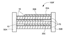
도 5a는 유전체 층들(20a)이 아직 형성되지 않은 소결 이전의 예시적인 MLCC(100G)를 예시한다. 구체적으로, 도 5a는 유전체 층들(20a)(도 1c에 예시됨)이 아직 형성되지 않았음을 의미하는 소결 이전의 그린 스테이지에서의 다른 예시적인 캐패시터 구조물(100G)을 도시한다. 이 예시적 실시예에서, Ag-유전체 복합물들(30A, 30B, 30C)(페이스트로부터 형성됨) 및 Ag/Pd 전극(10) 모두는 유전체 테잎(70)의 상단 상에 프린팅된다. Ag-유전체 복합물들(30A, 30B, 30C)은 전기 전류들의 단락을 방지하기 위하여 Ag/Pd 전극(10)의 영역에 비해 더 크게 프린팅된다. 도 5a의 이 예시적 실시예에서, 전극(10)의 표면적에 대해 복합물들(30A, 30B, 30C)의 표면적은 약 20% 더 크다. 캐패시터 구조물(100G)은 도 3에 예시된 것들과 동일한 재료로 만들어지는 유전체 테잎 층들(70)을 또한 갖는다.5A illustrates an
소결 후 도면: 금속 코팅된 유전체 테잎들을 사용하는 실제 샘플의 층 설계들 - 도 5b Drawing After Sintering: Layer Designs of Real Sample Using Metal Coated Dielectric Tapes-FIG. 5B
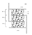
도 5b는 소결 이후의 예시적인 MLCC(100H)의 단면도를 예시한다. 구체적으로, 도 5b는 소결 이후의 캐패시터 구조물(100H)을 도시한다. 도 5b는 광학 현미경에 의하여 생성된 단면도이며, 소결 동안에 인-시튜로 유전체 층들(20a)을 형성하기 위하여 유전체 테잎들(70) 상에 프린팅되는 프린팅된 Ag-유전체 복합물(30)(도 2a-5a의 예비-소결 스테이지들에서 예시된 바와 같이 페이스트로부터 형성됨) 내의 은이 전극(10)으로 완전히 이동하도록 허용되는, 캐패시터 구조물(100H)의 예시적인 실시예를 예시한다. 도 5b에서, 더 밝게 음영처리된 재료는 Ag/Pd 전극 재료(10)인 반면, 어두운 배경 음영처리된 재료는 유전체 층들(70 및 20A)이다.5B illustrates a cross-sectional view of an example MLCC 100H after sintering. Specifically, FIG. 5B shows the capacitor structure 100H after sintering. FIG. 5B is a cross-sectional view produced by an optical microscope, and printed Ag-
도 5b에 도시된 바와 같이, (도 2a-5a의 예비-소결에서 예시된 바와 같은) Ag-복합물 층(30)의 은은 층(20A) 및 결과적인 캐패시터 구조물을 형성하기 위하여 전극 층(10)으로 완전히 이동(migrate or move)한다. 이 설명에서 사용되는 바와 같은 "인 시튜"는 "소결 동안"을 의미한다. 소결 동안 은 이동로부터 형성되는 프린팅된 얇은 캐패시터를 갖지 않는, 동일한 사이트를 갖고 전극들 및 유전체 층에 대해 동일한 재료들로 형성되는 종래의 캐패시터에 이 캐패시터 구조물(100G 및 100H)을 비교할 때, 캐패시턴스의 약 6배(약 600%)의 증가가 관찰된다. 유전 파괴 전압이 대개 얇은 유전체 층으로 인하여 저하되지 않음이 또한 유념된다.As shown in FIG. 5B, the silver layer of the Ag-composite layer 30 (as illustrated in the pre-sintering of FIGS. 2A-5A) may form the
상기 설명된 예시적인 실시예들에서, 캐패시턴스의 증가는 대개 Ag-유전체 복합물(30)로부터의 은 이동 이후에 얇은 유전체 층(20A)의 형성으로 인한 것이다. 그러나 전극(10)으로의 은의 이동은 또한 전극/유전체 계면에서 고르지 않은 표면을 형성할 기회들을 생성한다. 거친 표면은 대개 전극(10)의 표면적을 증가시키고, 캐패시턴스의 증가에 기여할 수 있다.In the exemplary embodiments described above, the increase in capacitance is usually due to the formation of thin
전극/유전체 계면에서 고르지 않은 표면을 야기하는 이들 변화들은 소결 온도에 의하여 영향을 받을 수 있다. 도 1c-5에 예시되는 캐패시터들의 예시적인 실시예들에서, 캐패시터들(100)이 더 낮은 온도에서 소성될 때 캐패시턴스의 약 10퍼센트의 증가가 관찰되었다.These changes resulting in an uneven surface at the electrode / dielectric interface can be affected by the sintering temperature. In exemplary embodiments of the capacitors illustrated in FIGS. 1C-5, an increase of about 10 percent of the capacitance was observed when the capacitors 100 were fired at lower temperatures.
캐패시터(100G 및 100H)는 Ag-유전체 복합물(30)을 순수 유전체로 교체함으로써 간단히 만들어질 수 있음이 주목되어야 한다. 이것은 은 퍼센트가 Ag-유전체 복합물(30)에서 제로에 접근할 때와 동등하다. 상기 예시적인 실시예들에서, 은은 Ag-유전체 복합물(30)의 금속으로서 사용된다. 비금속 MLCC의 Ni 및 Ni/Cu 및 귀금속 다중층 세라믹 캐패시터들(MLCC들)에서 사용되는 Ag/Pd 합금들과 같은(그러나 이에 제한되는 것은 아님) 다른 금속들 또는 합금들이 Ag-유전체 복합물(30)에 대하여 사용될 수 있다. 몇몇 경우들에서, Ag-유전체 복합물(30)의 금속 함량은 이동 이후의 전도성 층을 형성하기에 충분히 높아야 한다. 인 시튜로 형성된 유전체 층(20A), 예를 들어, 도 1c에 예시되는 유전체 층(20A), 도 5b의 유전체 층(30)의 두께에 영향을 미치는(affect or impact) 인자들은, 금속 유전체 복합물(30) 내의 금속 또는 합금의 용융점, 소결 온도, 및 금속 유전체 복합물(30)에서의 금속 함량의 양이다. 유전체(40) 또는 유전체(70)의 유리는 또한 인 시튜로 형성된 유전체 층들(20a)의 두께에 대해 상당한 영향력을 가질 수 있다.It should be noted that
테스트 샘플들의 소결 후 도면들: 금속 코팅된 유전체 테잎들을 사용하는 층 설계 - 도 6-13 Figures After Sintering of Test Samples: Layer Design Using Metal Coated Dielectric Tapes-FIGS. 6-13
도 6-13은 금속(즉, - Ag) 코팅된 유전체 테잎들을 사용하는 MLCC 층 설계들의 4개 샘플들의 밝은 현미경 도면들 및 주사 전자 현미경(SEM)의 흑백 사진들을 예시하였다. 이들 Ag 코팅된 유전체 테잎들은 MLCC의 층들을 형성하는 전체 유전체 두께의 대략 1/3을 만드는데 사용된다. 각각의 MLCC의 다른 2/3은 정상 유전체 테잎들을 포함한다. 이들 샘플들에서, 더 얇게 나타나는 하나의 층이 Ag 코팅된 유전체 테잎의 시트에 의하여 접촉되지 않은 것이 주목되었다. 전체 구조물이 전도성이 되었기 때문에, 작동/수행되지 않은 다른 테스트 샘플들과 마찬가지로, 이것은 전체 구조물이 전도성이 되는 것을 예방하기 위해 의도적으로 실행되었다.6-13 illustrate light microscopic drawings and black and white photographs of scanning electron microscopy (SEM) of four samples of MLCC layer designs using metal (ie-Ag) coated dielectric tapes. These Ag coated dielectric tapes are used to make approximately one third of the total dielectric thickness that forms the layers of the MLCC. The other two-thirds of each MLCC contains normal dielectric tapes. In these samples, it was noted that one thinner layer was not contacted by the sheet of Ag coated dielectric tape. Since the entire structure became conductive, like other test samples that were not operated / performed, this was done intentionally to prevent the entire structure from becoming conductive.
이들 샘플 MLCC들의 커버 층들은 또한 정상적 유전체 테잎들로 만들어진다. 지정된 100개의 MLCC들(A)은 배향이 동일하게 남아있도록 프로세싱되었으며, 그에 의해 내부 전극이 Ag 코팅된 유전체 테잎 위에 직접 프린팅되었다. 이들 부분들은 Ag 코팅된 층들이 아래쪽으로 향하도록, 번 아웃(burn out)되고 소결되었다. 번아웃 및 소성 동안(라벨 B) 코팅된 층들 각각이 (세터(setter)로부터 떨어져) 위쪽을 향하도록, 48개 MLCC들이 프로세싱되었다. 도 6-13에 예시되는 4개 샘플들의 각각의 그룹(A 및 B)은 2개 프로파일들, 940C/5시간 소결 및 975C/1시간 소결을 사용하여 세분(sub-divide)되고 소성된다.The cover layers of these sample MLCCs are also made of normal dielectric tapes. The designated 100 MLCCs (A) were processed so that the orientation remained the same, whereby the internal electrode was printed directly onto the Ag coated dielectric tape. These parts were burned out and sintered, with the Ag coated layers facing down. 48 MLCCs were processed so that each of the coated layers faced up (away from the setter) during burnout and firing (label B). Each group A and B of the four samples illustrated in FIGS. 6-13 is sub-divide and fired using two profiles, 940 C / 5 hour sintering and 975 C / 1 hour sintering.
도 6-13에 예시되는 샘플들에 대한 관찰들Observations on the samples illustrated in FIGS. 6-13
도 2c에 참조된 이전 샘플들에 비해 이 설계에 대한 소결된 마이크로구조에는 뚜렷한 향상이 존재하였다. 975*C/1시간 소결은 940* /5시간 프로파일보다 상당히 더 밀도가 높은 것으로 나타난다.There was a marked improvement in the sintered microstructure for this design over the previous samples referenced in FIG. 2C. The 975 * C / 1 hour sintering appears to be significantly denser than the 940 * / 5 hour profile.
결합제(binder) 번아웃 및 소성 동안의 배향과 무관하게, 도 6-13에 예시되는 각각의 샘플에서, 유전체 층(30)의 코팅된 테잎 부분 내의 Ag는 95Ag/5Pd 내부 전극(10)으로부터 실제로 멀리 이동하는 것으로 보여지며(이는 본 기술분야의 당업자에게 예기치 않은 결과임), 전기적 성능에 최소한의 영향력을 갖는 것으로 나타난다. 몇몇 층들에서 Ag가 중력에 대항하여 상향으로 이동되었기 때문에, 이것은 예기치 못한 것이다. 한편, 본 기술분야의 당업자는 중령으로 인하여 Ag가 하향으로 이동하는 것으로 예상할 것이다.Regardless of the orientation during binder burnout and firing, in each sample illustrated in FIGS. 6-13, the Ag in the coated tape portion of the
도 6-13에 예시되는 이들 샘플들에 대한 다른 관찰은, Ag 이동이 주로 코팅된 테잎 유전체 층(30) 내에 머무르는 것으로 나타나고 다소 순수한 유전체 층(20A)인 것으로 보이는 것처럼 군집한다(congregate)는 점이다. 은-유전체 복합물 내의 은은 전극 층으로 이동하고, 또한 Ag 금속의 포켓들(605)을 형성하기 위하여 이동한다. 이들 포켓들(605)은 더욱 빠른 프로파일 소결 트라이얼에서 훨씬 더 잦고(LT-3088A, sint. 975C/1h - 도 10-11 및 LT-3088B, sint. 940C/1h 도 12- 13), 그러나 더 느린 트라이얼에서 사이즈가 더 큰 것으로(LT-3088A, sint. 975C/5h - 도 6-7 및 LT- 3088B, sint. 940C/5h 도 8-9) 나타난다. 다시, 이것은 Ag의 상당 부분이 순수한 Ag의 포켓들(605)로서 축적되는 것을 제안한다. 이들 샘플들에 대한 다른 관찰은 샘플들 중 어느 것도 박리(delamination)들을 단면으로 보이지 않는다는 것이었다.Another observation for these samples illustrated in FIGS. 6-13 is that Ag migration appears to mainly reside in the coated
전기적 결과들(대략 1 kHz , 1 Vrms)Electrical results (approximately 1 kHz, 1 Vrms)
940℃/5hrs. 975℃/lhr.940 ° C./5hrs. 975 ° C./lhr.
LT-3088A 논-쇼트(non-shorts) 7/50 50/50 LT-3088A non-shorts 7/50 50/50
LT-3088B 논-쇼트 4/24 19/24
LT-3088B non-short 4/24 19/24
LT-3088A 캡 범위 (피코 F) 20.37 - 52.89 12.06 - 26.36 LT-3088A Cap Range (Pico F) 20.37-52.89 12.06-26.36
LT-3088B 캡 범위 (피코 F) 36.26 - 70.10 18.60 - 24.24
LT-3088B Cap Range (Pico F) 36.26-70.10 18.60-24.24
(A) 유효 유전 상수 84.76 42.67 (A) Effective dielectric constant 84.76 42.67
(B) 유효 유전 상수 113.5 39.24 (B) effective dielectric constant 113.5 39.24
가장 큰 캐패시턴스를 나타낸 각각의 그룹으로부터의 단일 파트에 대하여 유효 유전 상수가 계산되었다. 본 기술분야의 당업자에 의하여 이해되는 바와 같이, 유효 유전 상수는 캐패시터의 치수들 및 관찰된 캐패시턴스에 기반하여 계산된다. 940*C/5hrs에서 소결된 LT-3088A를 제외하고, 유전 손실은 각각의 그룹에 대해 약 0.00%로 측정되었으며, 유전 손실은 약 0.00 내지 약 0.03% 범위이다. 또한, 이들 범위들은 유효 층들의 정상 유전체 부분과 Ag 사이의 최소 반응을 제안한다.The effective dielectric constant was calculated for a single part from each group that exhibited the largest capacitance. As will be appreciated by those skilled in the art, the effective dielectric constant is calculated based on the dimensions of the capacitor and the observed capacitance. Except for LT-3088A sintered at 940 * C / 5hrs, dielectric loss was measured at about 0.00% for each group and dielectric loss ranged from about 0.00 to about 0.03%. These ranges also suggest a minimal response between Ag and the top dielectric portion of the effective layers.
한편, 이 유전체에 대하여 MLCC 형태의 정상 유전 상수(K)는 통상적으로 약 23이다. (내부 95Ag/5Pd 전극 층들을 갖지 않으나, MLCC의 것과 동일한 Ag 코팅된 유전체의 층들을 포함하는) K-스퀘어(square)들이 또한 이 동작(run)으로 만들어졌으며, 측정된 K는 대략 24.5인 것으로 발견되었다. 또, 이것은 Ag가 대체로 유전체와 비-반응성이며, 오히려(if anything), 본 기술분야의 당업자에 의하여 이해되는 바와 같이 이 형태의 전도에 크게 기여하지 않음을 제시한다.On the other hand, for this dielectric, the normal dielectric constant (K) in the MLCC form is typically about 23. K-squares (without inner 95Ag / 5Pd electrode layers, but including layers of the same Ag coated dielectric as those of MLCCs) were also made with this run, and the measured K was approximately 24.5. Found. This also suggests that Ag is largely non-reactive with the genome and, if anything, does not contribute significantly to this type of conduction, as understood by those skilled in the art.
도 6-13에 예시되고 하기에서 더욱 상세히 설명되는 샘플들에 대한 관찰들의 요약:Summary of observations for the samples illustrated in FIGS. 6-13 and described in more detail below:
금속-코팅된(즉, Ag-코팅된) 유전체 테잎들로부터 형성되는 MLCC 3-D 캐패시터는 전체 MLCC의 캐패시턴스 및 유효 유전 상수(K)를 상당히 증가시키는 것으로 보여진다. 상기 언급된 바와 같은 LT-3088B의 단일 경우에, 증가는 어떠한 금속-코팅된 유전체 테잎들도 없이 형성되는 MLCC에 대하여 대략 5배인 것으로 보여진다.MLCC 3-D capacitors formed from metal-coated (ie Ag-coated) dielectric tapes have been shown to significantly increase the capacitance and effective dielectric constant (K) of the entire MLCC. In the single case of LT-3088B as mentioned above, the increase is shown to be approximately 5 times for the MLCC formed without any metal-coated dielectric tapes.
도 6-13에 예시되는 4개 샘플들에 대한 상세한 설명Detailed description of the four samples illustrated in FIGS. 6-13
도 6-13은 상기 논의된 4개 샘플들을 예시한다. 각각의 샘플은 그것의 다양한 층들에 대해 다음의 참조 번호들을 사용한다: Ag 전극 층(10); Ag 전극 층(10)과 Ag 코팅된 유전체 테잎(30) 사이에 형성되는 유전체 층 (20A); Ag 금속의 포켓들(605); 및 코팅되지 않은 표준/정규 유전체 테잎(70).6-13 illustrate the four samples discussed above. Each sample uses the following reference numbers for its various layers:
구체적으로, 도 6a-6c는, 대략 5시간의 소킹(soaking) 동안 대략 940℃에서의 MLCC(100-1)의 소결 이후에, Ag 코팅된 유전체 테잎들(30)을 사용하는 제1 샘플 MLCC(100-1)(LT-3088A)의 주사 전자 현미경(SEM)에 의해 생성된 단면도들을 예시한다.Specifically, FIGS. 6A-6C illustrate a first sample MLCC using Ag coated
더욱 구체적으로, 도 6a는 대략 500배의 크기 레벨로 제1 샘플 MLCC(100-1)의 SEM 단면도를 예시한다. Ag 전극 층들(10), 유전체 층들(20a) 및 Ag 코팅된 유전체 테잎 층(30)을 포함하는, 층들의 수 개의 사례들이 존재한다. Ag 금속의 포켓들(605)이 또한 가시적이다.More specifically, FIG. 6A illustrates an SEM cross-sectional view of the first sample MLCC 100-1 at approximately 500 times the size level. There are several instances of layers, including Ag electrode layers 10, dielectric layers 20a and Ag coated
도 6b는 대략 2000배의 크기 레벨로 도 6a의 제1 샘플 MLCC(100-1)의 SEM 단면도를 예시한다. Ag 전극 층들(10), 유전체 층들(20a) 및 Ag 코팅된 유전체 테잎 층(30)을 포함하는, 가시적인 층들의 수 개의(그러나 도 6a에 예시된 것들보다 적은) 사례들 이 존재한다. Ag 금속의 포켓들(605)이 또한 가시적이다.FIG. 6B illustrates an SEM cross-sectional view of the first sample MLCC 100-1 of FIG. 6A at an approximately 2000-fold size level. There are several instances of visible layers (but less than those illustrated in FIG. 6A), including Ag electrode layers 10, dielectric layers 20a and Ag coated
도 6c는 대략 5000배의 크기 레벨로 도 6a의 제1 샘플 MLCC(100-1)의 SEM 단면도를 예시한다. Ag 코팅된 유전체 테잎 층(30)만이 가시적이다. 유전체 테잎 층(30) 내에 형성되는 Ag 금속의 포켓들(605)이 또한 가시적이다. 상기 언급된 바와 같이, 더 긴 소크 시간들을 갖는 이 예시적인 제1 샘플 MLCC(100-1)(및 제2 예시적 샘플 MLCC(100-2))의 금속(즉, - Ag)의 포켓들(605)은 더 긴 소크 시간들을 갖는 제3 및 제4 샘플 MLCC들(100-3, 100-4)의 포켓들(605)에 비해 사이즈가 더 크지만, 수가 더 적다(less frequent in number).FIG. 6C illustrates an SEM cross-sectional view of the first sample MLCC 100-1 of FIG. 6A at approximately 5000 times the size level. Only Ag coated
도 7a-7d는 도 6a-6c에 예시된 것에 대응하는 다른 샘플인 제1 샘플 MLCC들(100-1)(LT-3088A)의 광학 현미경에 의해 생성된 단면도들을 예시한다. 구체적으로, 도 7a-7c는 대략 100 배의 크기 레벨로 제1 샘플 MLCC(100-1)의 광학 현미경 단면도를 예시한다. 도 7a-7c에서, Ag 전극 층(10); Ag 코팅된 유전체 테잎(30); 및 코팅되지 않은 표준/정규 유전체 테잎(70)을 포함하는 수 개의 층들이 가시적이다. ((금속의 포켓들 또는 함유물들(605)은 가시적이지 않다.) 도 7a는 제1 샘플 MLCC(100-1)의 제1 실시예는 예시하는 반면, 도 7b는 제1 샘플 MLCC(100-1)의 제2 실시예를 예시하고, 도 7c는 제1 샘플 MLCC(100-1)의 제3 실시예를 예시하며, 여기서 각각의 실시예는 MLCC들(100)의 동일한 배치 또는 세트에서 제조된다.7A-7D illustrate cross-sectional views generated by an optical microscope of first sample MLCCs 100-1 (LT-3088A), another sample corresponding to that illustrated in FIGS. 6A-6C. Specifically, FIGS. 7A-7C illustrate optical microscopic cross-sectional views of first sample MLCC 100-1 at approximately 100 times the size level. 7A-7C,
도 7d는 대략 1000 배의 크기 레벨로 제1 샘플 MLCC(100-1)의 광학 현미경 단면도를 예시한다. 이 도 7d에서, Ag 전극 층들(10), 유전체 층들(20a) 및 Ag 코팅된 유전체 테잎 층(30)을 포함하는 수 개의 층들이 존재한다. Ag 금속의 포켓들(605)이 또한 가시적이다.FIG. 7D illustrates an optical microscope cross-sectional view of the first sample MLCC 100-1 at approximately 1000 times the size level. In this FIG. 7D, there are several layers including Ag electrode layers 10, dielectric layers 20a and Ag coated
도 8a-8c는 대략 5시간의 소킹 동안 대략 940C에서 MLCC를 소결한 이후, Ag 코팅된 유전체 테잎들을 사용하는 제2 샘플 MLCC(100-2)(LT-3088B)의 주사 전자 현미경(SEM)에 의하여 생성된 단면도들을 예시한다. 더욱 구체적으로, 도 8a은 대략 500 배의 크기 레벨로 제2 샘플 MLCC(100-2)의 SEM 단면도를 예시한다. Ag 전극 층들(10), 유전체 층들(20a) 및 Ag 코팅된 유전체 테잎 층(30)을 포함하는, 층들의 수 개의 사례들이 존재한다. Ag 금속의 포켓들(605)이 또한 가시적이다.8A-8C show scanning electron microscopy (SEM) of second sample MLCC 100-2 (LT-3088B) using Ag coated dielectric tapes after sintering MLCC at approximately 940C for approximately 5 hours of soaking. Illustrate the cross-sectional generated by. More specifically, FIG. 8A illustrates a SEM cross-sectional view of the second sample MLCC 100-2 at approximately 500 times the size level. There are several instances of layers, including Ag electrode layers 10, dielectric layers 20a and Ag coated
도 8b는 대략 2000 배의 크기 레벨로 도 8a의 제2 샘플 MLCC(100-2)의 SEM 단면도를 예시한다. Ag 전극 층들(10), 유전체 층들(20a) 및 Ag 코팅된 유전체 테잎 층(30)을 포함하는, 가시적인 층들의 수 개의(그러나 도 8a에 예시된 것들보다는 적은) 사례들이 존재한다. Ag 금속의 포켓들(605)은 또한 가시적이다.FIG. 8B illustrates an SEM cross-sectional view of the second sample MLCC 100-2 of FIG. 8A at an approximately 2000-fold size level. There are several instances of visible layers (but less than those illustrated in FIG. 8A), including Ag electrode layers 10, dielectric layers 20a and Ag coated
도 8c는 대략 5000 배의 크기 레벨로 도 8a의 제2 샘플 MLCC(100-2)의 SEM 단면도를 예시한다. 단지 Ag 코팅된 유전체 테잎 층(30)만이 가시적이다. 유전체 테잎 층(30) 내에 형성되는 Ag 금속의 포켓들(605)이 또한 가시적이다. 상기 논의된 바와 같이, 더 긴 소크 시간들을 갖는 이 예시적인 제2 샘플 MLCC(100-2)(및 제1 예시적 샘플 MLCC(100-1))의 금속(예를 들어, Ag)의 포켓들(605)은 더 긴 소크 시간들을 갖는 제3 및 제4 샘플 MLCC들(100-3, 100-4)의 포켓들(605)에 비하여 사이즈가 더 크지만, 개수가 더 적다.FIG. 8C illustrates an SEM cross-sectional view of the second sample MLCC 100-2 of FIG. 8A at an approximately 5000-fold size level. Only Ag coated
도 9a-9d는 도 8a-8c에 예시되는 제2 샘플 MLCC(100-2)(LT-3088B)에 대응하는 다른 제2 샘플들의, 광학 현미경에 의하여 생성된 단면도들을 예시한다. 구체적으로, 도 9a-9c는 대략 100 배의 크기 레벨로 제2 샘플 MLCC(100-2)의 광학 현미경 단면도를 예시한다. 도 9a-9c에서, Ag 전극 층(10); Ag 코팅된 유전체 테잎(30); 및 코팅되지 않은 표준/정규 유전체 테잎(70)을 포함하는 수 개의 층들이 가시적이다. (금속의 포켓들 또는 함유물들(605)은 가시적이지 않다.) 도 9a는 제2 샘플 MLCC(100-2)의 제1 실시예를 예시하는 반면, 도 9b는 제2 샘플 MLCC(100-2)의 제2 실시예를 예시하고, 도 9c는 제2 샘플 MLCC(100-2)의 제3 실시예를 예시하며, 각각의 실시예는 MLCC들(100)의 동일한 배치 또는 세트에서 제조되었다.9A-9D illustrate cross-sectional views generated by an optical microscope of other second samples corresponding to second sample MLCC 100-2 (LT-3088B) illustrated in FIGS. 8A-8C. Specifically, FIGS. 9A-9C illustrate optical microscopic cross-sectional views of second sample MLCC 100-2 at approximately 100-fold size levels. 9A-9C, an
도 9d는 대략 1000 배의 크기 레벨로 제2 샘플 MLCC(100-2)(LT-3088B)의 광학 현미경 단면도를 예시한다. 이 도 9d에서, Ag 전극 층들(10), 유전체 층들(20a) 및 Ag 코팅된 유전체 테잎 층(30)을 포함하는 수 개의 층들이 존재한다. Ag 금속의 포켓들(605)이 또한 가시적이다.9D illustrates an optical microscope cross-sectional view of the second sample MLCC 100-2 (LT-3088B) at approximately 1000 times the size level. In this FIG. 9D, there are several layers including Ag electrode layers 10, dielectric layers 20a and Ag coated
도 10a-10c는 대략 한 시간의 소킹 동안 대략 975C에서 MLCC(100-3)의 소결 이후에, Ag 코팅된 유전체 테잎들(30)을 사용하는 제3 샘플 MLCC(100-3)(LT-3088A)의, 주사 전자 현미경(SEM)에 의하여 생성된 단면도들을 예시한다. 더욱 구체적으로, 도 10a는 대략 500 배의 크기 레벨로 제3 샘플 MLCC(100-3)의 SEM 단면도를 예시한다. Ag 전극 층들(10), 유전체 층들(20a) 및 Ag 코팅된 유전체 테잎 층(30)을 포함하는, 층들의 수 개의 사례들이 존재한다. Ag 금속의 포켓들(605)이 또한 가시적이다.10A-10C illustrate a third sample MLCC 100-3 (LT-3088A) using Ag coated
도 10b는 대략 2000 배의 크기 레벨로 도 10a의 제3 샘플 MLCC(100-3)의 SEM 단면도를 예시한다. Ag 전극 층들(10), 유전체 층들(20a) 및 Ag 코팅된 유전체 테잎 층(30)을 포함하는, 가시적인 층들의 수 개의(그러나 도 10a에 예시된 것들보다는 적은) 사례들이 존재한다. Ag 금속의 포켓들(605)이 또한 가시적이다.FIG. 10B illustrates an SEM cross-sectional view of the third sample MLCC 100-3 of FIG. 10A at an approximately 2000-fold size level. There are several instances of visible layers (but fewer than those illustrated in FIG. 10A), including Ag electrode layers 10, dielectric layers 20a and Ag coated
도 10c는 대략 5000 배의 크기 레벨로 도 10a의 제3 샘플 MLCC(100-3)의 SEM 단면도를 예시한다. 단지 Ag 코팅된 유전체 테잎 층(30)만이 가시적이다. 유전체 테잎 층(30) 내에 형성되는 유전체 테잎 층(30)이 또한 가시적이다. 상기 언급된 바와 같이, Ag 금속의 포켓들(605)은 제1 및 제2 샘플 MLCC(100-1, 100-2)의 더 느린 소킹에 비해 소결 제3 샘플 MLCC(100-3)(및 제4 샘플(100-4))의 이러한 더 빠른 소킹에서 훨씬 더 빈번하게 나타나지만, 사이즈가 더 작다.FIG. 10C illustrates an SEM cross-sectional view of the third sample MLCC 100-3 of FIG. 10A at an approximately 5000-fold size level. Only Ag coated
도 11a-11d는 도 10a-10c에 예시되는 제3 샘플 MLCC(100-3)(LT-3088A)에 대응하는 다른 제3 샘플의, 광학 현미경에 의하여 생성된 단면도들을 예시한다. 구체적으로, 도 11a-11c는 대략 100 배의 크기 레벨로 제3 샘플 MLCC(100-3)의 광학 현미경 단면도를 예시한다. 도 11a에서, Ag 전극 층(10); Ag 코팅된 유전체 테잎(30); 및 코팅되지 않은 표준/정규 유전체 테잎(70)을 포함하는 수 개의 층들이 가시적이다. (금속의 포켓들 또는 함유물들(605)은 가시적이지 않다.) 도 11a는 제3 샘플 MLCC(100-3)의 제1 실시예를 예시하는 반면, 도 11b는 제3 샘플 MLCC(100-3)의 제2 실시예를 예시하고, 도 11c는 제3 샘플 MLCC(100-3)의 제3 실시예를 예시하며, 각각의 실시예는 MLCC들(100)의 동일한 배치 또는 세트에서 제조되었다.11A-11D illustrate cross-sectional views generated by an optical microscope of another third sample corresponding to the third sample MLCC 100-3 (LT-3088A) illustrated in FIGS. 10A-10C. Specifically, FIGS. 11A-11C illustrate optical microscopic cross-sectional views of third sample MLCC 100-3 at approximately 100-fold size levels. In FIG. 11A, the
도 11d는 대략 1000 배의 크기 레벨로 제3 샘플 MLCC(100-3)의 광학 현미경 단면도를 예시한다. 이 도 11d에서, Ag 전극 층들(10), 유전체 층들(20a) 및 Ag 코팅된 유전체 테잎 층(30)을 포함하는 수 개의 층들이 존재한다. Ag 금속의 포켓들(605)이 또한 가시적이다.FIG. 11D illustrates an optical microscope cross-sectional view of third sample MLCC 100-3 at approximately 1000 times the size level. In this FIG. 11D, there are several layers including Ag electrode layers 10, dielectric layers 20a and Ag coated
도 12a-12c는 대략 1시간의 소킹 동안 대략 975C에서의 MLCC의 소결 이후에, 주사 전자 현미경(SEM)에 의하여 생성된, Ag 코팅된 유전체 테잎들을 사용하는 제4 샘플 MLCC(100-4)의 단면도들을 예시한다. 더욱 구체적으로, 도 12a는 대략 500 배의 크기 레벨로 제4 샘플 MLCC(100-4)의 SEM 단면도를 예시한다. Ag 전극 층들(10), 유전체 층들(20a) 및 Ag 코팅된 유전체 테잎 층(30)을 포함하는, 층들의 수 개의 사례들이 존재한다. Ag 금속의 포켓들(605)이 또한 가시적이다.12A-12C show a fourth sample MLCC 100-4 using Ag coated dielectric tapes produced by scanning electron microscopy (SEM) after sintering of MLCC at approximately 975C for approximately one hour of soaking. Illustrate cross sections. More specifically, FIG. 12A illustrates a SEM cross-sectional view of fourth sample MLCC 100-4 at approximately 500 times the size level. There are several instances of layers, including Ag electrode layers 10, dielectric layers 20a and Ag coated
도 12b는 대략 2000 배의 크기 레벨로 도 12a의 제4 샘플 MLCC(100-4)(LT-3088B)의 SEM 단면도를 예시한다. Ag 전극 층들(10), 유전체 층들(20a), 및 Ag 코팅된 유전체 테잎 층(30)을 포함하는, 가시적인 층들의 수 개의(그러나 도 12a에 예시된 것들보다는 적은) 사례들이 존재한다. Ag 금속의 포켓들(605)이 또한 가시적이다.FIG. 12B illustrates an SEM cross-sectional view of the fourth sample MLCC 100-4 (LT-3088B) of FIG. 12A at an approximately 2000-fold size level. There are several instances of visible layers (but fewer than those illustrated in FIG. 12A), including Ag electrode layers 10, dielectric layers 20a, and Ag coated
도 12c는 대략 5000 배의 크기 레벨로 도 12a의 제4 MLCC(100-4)의 SEM 단면도를 예시한다. 단지 Ag 코팅된 유전체 테잎 층(30)만이 가시적이다. 유전체 테잎 층(30) 내에 형성되는 Ag 금속의 포켓들(605)이 또한 가시적이다. 상기 언급된 바와 같이, Ag 금속의 포켓들(605)은 제1 및 제2 샘플 MLCC(100-1, 100-2)의 더 느린 소킹에 비해 소결 제4 샘플 MLCC(100-4)(및 제3 샘플(100-3))의 이러한 더 빠른 소킹에서 훨씬 자주 나타나지만, 사이즈가 더 작다.FIG. 12C illustrates a SEM cross-sectional view of the fourth MLCC 100-4 of FIG. 12A at an approximately 5000-fold size level. Only Ag coated
도 13a-13d는 도 12a-12c에 예시되는 제4 샘플 MLCC(100-4)(LT-3088A)에 대응하는 다른 제4 샘플들의, 광학 현미경에 의해 생성된 단면도들을 예시한다. 구체적으로, 도 13a-13c는 대략 100 배의 크기 레벨로 제4 샘플 MLCC(100-4)의 광학 현미경 단면도를 예시한다. 도 13a-13c에서, Ag 전극 층(10); Ag 코팅된 유전체 테잎(30); 및 코팅되지 않은 표준/정규 유전체 테잎(70)을 포함하는 수 개의 층들이 가시적이다. (금속의 포켓들 또는 함유물들(605)은 가시적이지 않다.) 도 13a는 제4 샘플 MLCC(100-4)의 제1 실시예를 예시하는 반면, 도 13b는 제4 샘플 MLCC(100-4)의 제2 실시예를 예시하고, 도 13c는 제4 샘플 MLCC(100-4)의 제3 실시예를 예시하며, 각각의 실시예는 MLCC들(100)의 동일한 배치 또는 세트에서 제작되었다.13A-13D illustrate cross-sectional views generated by an optical microscope of other fourth samples corresponding to fourth sample MLCC 100-4 (LT-3088A) illustrated in FIGS. 12A-12C. Specifically, FIGS. 13A-13C illustrate optical microscopic cross-sectional views of fourth sample MLCC 100-4 at approximately 100-fold size levels. 13A-13C,
도 13d는 대략 1000 배의 크기 레벨로 제4 샘플 MLCC(100-4)의 광학 현미경 단면도를 예시한다. 이 도 13d에서, Ag 전극 층들(10), 유전체 층들(20a) 및 Ag 코팅된 유전체 테잎 층(30)을 포함하는 수 개의 층들이 존재한다. Ag 금속의 포켓들(605)이 또한 가시적이다.FIG. 13D illustrates an optical microscope cross-sectional view of fourth sample MLCC 100-4 at approximately 1000 times the size level. In this FIG. 13D, there are several layers including Ag electrode layers 10, dielectric layers 20a and Ag coated
도 14-22의 3-D 캐패시터들을 구성하기 위한 고유 컴포넌트 선택과 결합된 변형된 제조 프로세스: 금속 코팅된 세라믹 입자들 Modified manufacturing process combined with unique component selection to construct the 3-D capacitors of FIGS. 14-22: metal coated ceramic particles
상기 설명된 예시적인 코팅되지 않은 세라믹 파우더(205) 대신에 금속 코팅된 세라믹 입자들을 사용함으로써, 변형된 세라믹 캐패시터 제조 방법(101)이 또한 3-차원 캐패시터 실시예들을 생성하는데 사용될 수 있다.By using metal coated ceramic particles instead of the exemplary uncoated ceramic powder 205 described above, the modified ceramic
은 코팅된 유전체들과 같은(그러나 이에 제한되는 것은 아님) 연속하는 미립자 코팅을 특징으로 하는 금속-코팅된 세라믹 파우더들이 3-차원 MLCC의 다양한 실시예들에서 이용된다. 은 코팅된 유리 비드들은 현재 펜실베니아 맬버른의 Technic, Inc. of Woonsocket, Rhode Island 및 Potters Industries, Inc.로부터 입수가능하다.Metal-coated ceramic powders that feature a continuous particulate coating, such as but not limited to silver coated dielectrics, are used in various embodiments of a three-dimensional MLCC. Silver coated glass beads are currently manufactured by Technic, Inc. of Melbourne, Pennsylvania. of Woonsocket, Rhode Island and Potters Industries, Inc.
통상적으로, 금속-코팅된 세라믹 파우더의 금속 코팅은 전도성 파우더와 부합하며, 상기 전도성 파우더는 귀금속 MLCC의 경우에 은 또는 은-팔라듐 합금 그리고 비금속 MLCC의 경우에 니켈 또는 니켈 합금들과 같은(그러나 이에 제한되는 것은 아님) 전극 층을 생성하는데 사용될 수 있다. 다른 실시예들에서, 부합하지 않는 결함이 있는 코팅들을 갖는 금속-코팅된 세라믹 파우더들이 이용될 수 있다. 또한, 파우더가 주어진 3-차원 캐패시터 실시예로 통합되기 이전에 몇몇 금속-코팅된 세라믹 파우더들에서 미립자 코팅이 실질적으로 부합됨에도 불구하고, 코팅의 지속성에 있어서의 결함들이 금속 코팅된 세라믹 미립자들을 페이스트들로 혼합하는 프로세스 동안에 발생할 수 있다. 코팅된 미립자가 연속적인 부합하는 코팅 또는 부합하지 않는 결함이 있는 코팅을 특징으로 하는지와 무관하게, 코팅된 미립자는 3-차원 캐패시터 실시예의 유전체 층을 효과적으로 형성하는데 사용될 수 있다.Typically, the metal coating of the metal-coated ceramic powder is consistent with the conductive powder, which is (but is not limited to) silver or silver-palladium alloys for precious metal MLCCs and nickel or nickel alloys for nonmetallic MLCCs. But not limited to, electrode layers. In other embodiments, metal-coated ceramic powders with mismatched defective coatings may be used. Also, although the particulate coating is substantially consistent in some metal-coated ceramic powders before the powder is incorporated into a given three-dimensional capacitor embodiment, defects in the durability of the coating paste the metal coated ceramic particulates. May occur during the mixing process. Regardless of whether the coated microparticles are characterized by a continuous matching coating or a non-matching defective coating, the coated microparticles can be used to effectively form the dielectric layer of a three-dimensional capacitor embodiment.
바람직하게, 금속 코팅과 세라믹 미립자 기판 사이의 내재적 표면 장력으로 인하여, 소결 온도로의 노출의 결과로서 금속 코팅의 불연속성이 발생할 수 있다. 본 기술분야의 당업자는 주어진 소결 온도로의 금속-코팅된 미립자의 노출이 금속 코팅으로 하여금 미립자로부터 유동하고 이웃 미립자들 사이에 보이드(void)들에 집합되게(aggregate) 할 수 있음을 이해할 것이다. 유전체 미립자의 표면으로부터 유동된 금속 코팅의 결과적인 집합체(aggregation)들은 나란히 놓인 유전체 미립자 사이에 캐비티들로 안착하고, 동시에 MLCC 내의 애노드 또는 캐소드 층에 접촉할 수 있으며, 그에 의해 전극 층으로부터 유전체 층 내로 실질적으로 수직하게 돌출하는 애노드 또는 캐소드 층의 전도성 연장부를 효율적으로 생성한다. 특히, 그리고 바람직하게, 집합된 금속 코팅의 다수의 돌출부들은 전도성 층들에 기인하는 표면적의 증가에 의해서, MLCC의 전체 공간 풋프린트의 확장 없이, MLCC의 용량성 밀도를 증가시키는 역할을 한다. 소결 이후에, 금속 코팅들의 몇몇 집합체들로부터 초래될 수 있는 돌출부의 두께는, 약 0.001 미크론 내지 약 10 미크론 범위인 전체 입자 두께의 1% 내지 90%인 것으로 여겨진다.Preferably, due to the inherent surface tension between the metal coating and the ceramic particulate substrate, discontinuity of the metal coating may occur as a result of exposure to the sintering temperature. Those skilled in the art will appreciate that exposure of metal-coated fine particles to a given sintering temperature may cause the metal coating to flow out of the fine particles and aggregate into voids between neighboring fine particles. The resulting aggregates of the metal coating flowed from the surface of the dielectric particulate can rest in cavities between the dielectric particulate lying side by side and at the same time contact the anode or cathode layer in the MLCC, thereby from the electrode layer into the dielectric layer. Efficiently create conductive extensions of the anode or cathode layer that protrude substantially vertically. In particular, and preferably, the plurality of protrusions of the aggregated metal coating serves to increase the capacitive density of the MLCC without increasing the overall spatial footprint of the MLCC by increasing the surface area due to the conductive layers. After sintering, the thickness of the protrusions that may result from some aggregates of metal coatings is believed to be 1% to 90% of the total particle thickness, ranging from about 0.001 microns to about 10 microns.
본 기술분야의 당업자는, 다양한 제조 및 재료 파라미터들이 코팅된 유전체 미립자로부터의 전도성 코팅의 집합 및 유동을 제어하기 위하여 레버리징될 수 있으며, 따라서 특정 프로세스 파라미터 설정 조합들 또는 재료 피쳐들이 신규하거나 또는 신규한 결과들을 만들어낼 수 있더라도, 프로세스 파라미터 설정 또는 재료 피쳐들에 있어서의 변경들이 본 개시물의 범위를 제한하지 않을 것임을 인식할 것이다. 금속-코팅된 미립자로부터의 금속 코팅의 집합 및 유동에 영향을 미치도록 레버리징될 수 있는 제조 파라미터들 및 재료 피쳐들은 금속 코팅 퍼센트, 유전체 층의 두께, 소결 온도 및 소결 시간을 포함한다(그러나 이에 제한되는 것은 아님).One skilled in the art can appreciate that various manufacturing and material parameters can be leveraged to control the aggregation and flow of conductive coatings from the coated dielectric particulate, so that specific process parameter setting combinations or material features are new or novel. Although one result may be produced, it will be appreciated that changes in process parameter settings or material features will not limit the scope of this disclosure. Fabrication parameters and material features that can be leveraged to affect the aggregation and flow of metal coatings from metal-coated particulates include, but are not limited to, metal coating percent, dielectric layer thickness, sintering temperature, and sintering time. Not limited).
3-차원 캐패시터의 몇몇 실시예들은 코어-쉘(core-shell) 세라믹 입자들로 구성되는 유전체 재료 선택을 레버리징할 수 있다. 몇몇 실시예들에서, 코어-쉘 세라믹 입자의 코어는 BaTi03의 조성물을 가질 수 있는 한편, 쉘들은 캐패시턴스의 온도 계수들을 변형하기 위하여 도펀트들이 풍부할 수 있다. 조성 분포(코어-쉘 구조)는 요구되는 온도 범위에 걸쳐 일관된 유전 상수를 제공할 수 있다.Some embodiments of three-dimensional capacitors may leverage dielectric material selection consisting of core-shell ceramic particles. In some embodiments, the core of the core-shell ceramic particle may have a composition of BaTi0 3 , while the shells may be rich in dopants to modify the temperature coefficients of the capacitance. The composition distribution (core-shell structure) can provide a consistent dielectric constant over the required temperature range.
도 14는 3-차원 캐패시터의 예시적 일 실시예를 형성할 수 있는 단일 EDE 삼중-층(300)의 단면도를 예시하며, 여기서 금속 집합체들 (함유물들) 형태의 3-차원 구조물들(돌출부들)은 유전체 미립자들 상의 전도성 코팅들로부터 형성된다. 유전체 층(305)은 예를 들어, 금속 코팅된 세라믹 입자들(315)을 포함할 수 있으며, 여기서 세라믹 미립자 상의 전도성 금속 코팅은 은-팔라듐 합금들, 팔라듐, 팔라듐 합금들, 백금, 백금 합금들, 은, 은 합금들, 금, 금 합금들 등을 포함할 수 있다(그러나 이에 제한되는 것은 아님). EDE 삼중-층(300)의 몇몇 구현예들에서, 유전체 층과의 금속의 체적 분율은 예를 들어, 적어도 약 10%, 또는 적어도 약 20%, 또는 적어도 약 30%, 또는 적어도 약 40%, 예를 들어, 약 40% 내지 약 60%의 범위에 있을 수 있다. 유전체 미립자 상에 은-팔라듐 코팅을 포함할 수 있는 실시예들의 비-제한적 예로서, 은-팔라듐 코팅의 중량 퍼센트 조성은 약 95%Ag 내지 약 5%Pd, 더욱 바람직하게는 약 90%Ag 내지 약 10%Pd, 그리고 가장 바람직하게는 약 70%Ag 내지 약 30%Pd의 범위에 있을 수 있다.FIG. 14 illustrates a cross-sectional view of a single EDE triple-
몇몇 실시예들에서 사용되는 유전체 미립자 상의 전도성 금속 코팅은 이리듐, 로듐 및 루테늄과 같은(그러나 이에 제한되는 것은 아님) 다른 귀금속들 및 그들의 개별적 합금들을 포함할 수 있다. 부가적으로, 몇몇 실시예들은 구리, 니켈, 철, 코발트, 망간, 티타늄, 아연과 같은(그러나 이에 제한되는 것은 아님) 비금속들을 포함하는 금속 코팅을 갖는 미립자를 포함할 수 있다. 게다가, 또 다른 실시예들은 텅스텐, 몰리브덴, 지르코늄, 탄탈룸, 및 니오븀과 같은(그러나 이에 제한되는 것은 아님) 내화 금속들로 코팅되는 유전체 미립자를 포함할 수 있는 것으로 계획된다.The conductive metal coating on the dielectric particulate used in some embodiments may include other precious metals such as, but not limited to iridium, rhodium and ruthenium and their respective alloys. In addition, some embodiments may include particulates having a metal coating comprising nonmetals such as, but not limited to, copper, nickel, iron, cobalt, manganese, titanium, zinc. In addition, it is contemplated that other embodiments may include dielectric particulate coated with refractory metals such as, but not limited to tungsten, molybdenum, zirconium, tantalum, and niobium.
또한, 예시적인 유전체 층(305)이 코팅된 세라믹 입자들을 포함하는 것으로서 설명되나, 층(305)의 코팅된 입자들의 유전체 부분은 은-코팅된 세라믹들, 팔라듐-코팅된 세라믹들, 은 팔라듐-코팅된 세라믹들 등과 같은(그러나 이에 제한되는 것은 아님) 세라믹들을 제외한 유전체 물질뿐 아니라, 은 코팅된 포뮬레이팅된 티탄산 바륨 기반 유전체들, 은 코팅된 유리 비드들, 및 알루미나 및 탄탈룸 산화물과 같은(그러나 이에 제한되는 것은 아님) 무기 산화물들을 포함할 수 있는 것으로 또한 계획된다. 또한, 세라믹 입자들(315) 상의 금속 코팅(320)은 유전체 그린 시트의 생성 이전에 실질적으로 균일할 수 있으나(미도시), 금속 코팅(320)은 바람직하게는 소결 이후에 불연속적이 된다.Also, while the
유전체 층(305)은 2개의 전극 플레이트들(310A, 310C) 사이에 위치설정되는 세라믹 입자들(315)의 전체 층으로서 도시된다. 특히, 도 14의 예시에 플레이트(310A)가 애노드 플레이트를 표현하는 것으로 지정되고 플레이트(310C)는 캐소드 플레이트로서 지정되었으나, 본 기술분야의 당업자는 전도성 플레이트(310)가 애플리케이션이 요구할 수 있는 바에 따라 충전된 캐패시터에서 애노드로서 또는 캐소드로서 수행할 수 있음을 이해할 것이다. 유전체 층(305)의 세라믹 입자들은 통상적으로 사이즈가 약 0.01 내지 약 10 미크론의 범위이나, 본 기술분야의 당업자에 의하여 이해되는 바와 같이 다른 유전체 입자 사이즈도 가능하다.
상기 설명된 바와 같이, 세라믹 칩들의 소결 이후에 금속 코팅(320)의 불연속성은 주로 금속 및 세라믹과 같은(그러나 이에 제한되는 것은 아님), 코팅된 유전체 입자들(315)의 다른 재료들 간의 표면 장력으로 인한 것이다. 일반적으로, 소결 온도에 도달된 이후, 상기 온도는 금속 코팅(320)으로 하여금 유전체 세라믹 입자들(315) 사이의 캐비티들(325)로 유동하고 집합하게 한다. 바람직하게, 용융된 미립자 코팅으로부터 초래되는 집합된 금속(320)은 애노드(310A) 플레이트 또는 캐소드(310C) 플레이트 중 어느 하나로부터 유전체 층을 통해 아래로 실질적으로 수직하게 연장되거나 돌출되는 다수의 3-차원 구조물들 또는 돌출부들(320)을 형성하기 위하여 냉각될 것이다. 전도성 재료를 포함하는 3-차원 구조물들(320)은, EDE 삼중-층(300)의 애노드(310A) 플레이트 또는 캐소드(310C) 플레이트 중 하나를 갖는 계면 구조물(330)을 형성할 수 있다. 본 기술분야의 당업자는, 전도성 플레이트들(310A, 310C)에 기인하는 전체 표면적들이 효율적으로 증가될 수 있고(유전체 재료는 모두 유전체 입자들(315) 사이로 확산됨), 따라서 캐패시터(300)의 전체 용량성 밀도를 증가시킬 수 있음을 이해할 것이다.As described above, the discontinuity of the
용량성 밀도의 비-제한적 예가 증가함에 따라, 3-차원 캐패시터의 실시예들은 종래의 캐패시터 설계들에 대해 약 10배 내지 약 1000배 정도의 증가된 용량 밀도를 갖는 것으로 추정되었다. 그렇기는 하지만, 용량 밀도 증가의 상기 범위는 예시를 목적으로 제공되며, 개시물의 범위에 대한 제한 요인이 아닐 것이다. 본 기술분야의 당업자는 주어진 3-차원 캐패시터 실시예가 바람직하게는, 동등한 또는 거의 동등한 회로에서의 공간 풋 프린트를 요구하는 다른 용량 설계들에 비교할 때 증가된 용량 밀도를 가질 수 있음을 인식할 것이다.As non-limiting examples of capacitive densities have increased, embodiments of three-dimensional capacitors have been estimated to have increased capacities densities of about 10 to about 1000 times over conventional capacitor designs. Nevertheless, the above range of capacity density increase is provided for illustrative purposes and will not be a limiting factor on the range of the disclosure. Those skilled in the art will appreciate that a given three-dimensional capacitor embodiment may preferably have an increased capacity density when compared to other capacity designs that require a spatial footprint in an equivalent or near equivalent circuit.
중요하게, 본 기술분야의 당업자는, 유전체 층(305) 및 전도성 층(310)에 실질적으로 직각인 것들을 제외한 각도들이 유전체 미립자 코팅(315)의 집합체의 결과로서 계획되고, 이로써, 다양한 층들에 실질적으로 직각인 3-차원 구조물들(330)에 대한 상기 설명이 3-차원 캐패시터(300)의 범위를 제한하지 않을 것임을 이해할 것이다. 형성되는 3-차원 구조물들(315, 320) 양자 모두는 주어진 컨덕터 플레이트에 기인하는 전체 표면적을 증가시키고, 또한 본질적으로 주어진 EDE 삼중-층(300) 내의 다수의 작은 마이크로-캐패시터 삼중-층 배열들을 형성한다.Importantly, one of ordinary skill in the art would be aware that angles other than those substantially perpendicular to
상기 설명된 예시적인 실시예와 같은 3-차원 캐패시터(315)를 생성하기 위하여 유전체 층(305)에서 사용하기에 적합한 금속-코팅된 세라믹 파우더들이 상업적으로 제조될 수 있다. 특정 조합들이 다른 조합들에 비해 더욱 바람직할 수 있으나, 혁신적인 캐패시터 구조물은 다양한 유전체 미립자 재료들 및 코팅 조합들을 포함할 수 있다. 또한, 본 기술분야의 당업자는 다양한 파라미터들이, 금속 코팅 퍼센트, 소결 온도 및 소결 시간의 선택과 같은(그러나 이에 제한되는 것은 아님) 3-차원 캐패시터의 3-차원 구조물들의 양상들 또는 특성들을 제어하는데 사용될 수 있음을 인식할 것이다.Metal-coated ceramic powders suitable for use in
도 15는 3-차원 캐패시터의 예시적 일 실시예를 형성하는 단일 EDE 층(400)의 단면도를 예시하며, 여기서 3-차원 구조물들은 유전체 입자들 또는 코팅된 유전체 입자들의 유전체 슬러리로 혼합된 금속 입자들(421)로 형성된다. 상기 설명된 방법(101)의 단계(120)에 부합하여, 전극 플레이트들(410A, 410C)이 그린 테잎(215, 405) 위에 프린팅되며, 여기서 그린 테잎(215, 405)은 순수한 유전체 슬러리(210)로 만들어지는 대신 금속 미립자(421) 및 유전체 입자들 또는 금속 코팅된 유전체 미립자(415)의 혼합물로 만들어진다. 도 14 실시예와 관련하여 상기 설명된 바와 같이, 금속 코팅된 유전체 미립자는 전도성 코팅 및 유전체 미립자의 임의의 조합물을 포함할 수 있는 것으로 계획되며, 이로써, 특정 미립자 및 전도성 코팅 재료 선택들 및 조합들이 본 명세서에서 예시를 목적으로 제공되고, 개시물의 범위를 제한하지 않을 것임이 이해될 것이다. 유사하게, 금속 미립자(421)는 은, 은 팔라듐 합금, 니켈, 니켈 합금들, 구리, 구리 합금들 등을 포함하는(그러나 이에 제한되는 것은 아님) 임의의 적절한 전도성 재료를 포함할 수 있는 것으로 계획된다. 유전체 입자들(415)의 금속 코팅은 금속 미립자(421)와의 기계적 혼합으로부터의 결과로서 불연속적일 수 있으나, 소결 이후, 코팅은 일반적으로, 3-차원 구조물들 또는 돌출부들(420)이 실질적으로 유전체 층에 수직으로 형성되고, 일부는 상단 전극과의 계면(430A) 상에 형성하고, 일부는 계면(430B) 상에 하단 전극과 연결되게 형성하도록, 유동하고 집합할 것이며, 금속 미립자(421)는 도처에 집합된다.15 illustrates a cross-sectional view of a
도 14에 예시되는 3-차원 캐패시터 층의 제조는 방법(101)에 관하여 설명된 것과 본질적으로 동등하다. 또. 도 14에 예시된 예시적인 실시예의 3-차원 캐패시터를 제조하기 위하여, 대개 도 1-2와 함께 설명된 바와 같은 제조 프로세스에 대한 변형들이 이루어진다. 구체적으로, 단계(105)에서, 금속 코팅된 유전체(315)가 MLCC 제품에서 세라믹 유전체 파우더(205) 대신에 사용된다면, 결과적인 3-차원 캐패시터는 도 14 실시예와 유사한 구조를 가질 것이다. 유사하게, 전도성 미립자(421) 및 유전체 입자들 또는 코팅된 유전체 미립자(415)의 기계적 혼합물이 파우더(205) 대신에 삽입된다면, 결과적인 3-차원 캐패시터는 도 15 실시예와 유사한 구조를 가질 것이다.The manufacture of the three-dimensional capacitor layer illustrated in FIG. 14 is essentially equivalent to that described with respect to
고유 컴포넌트 선택 및 부가적인 제조 단계들Unique component selection and additional manufacturing steps
다양한 신규한 컴포넌트 선택들을 수용하기 위한 부가적인 제조 단계들의 통합에 의하여, 고유 세라믹 캐패시터 제조 방법(101)이 3-차원 캐패시터들을 생성하는데 사용될 수 있다.By incorporating additional manufacturing steps to accommodate various novel component choices, a unique ceramic
도 16은 3-차원 캐패시터의 예시적인 실시예를 형성할 수 있는 단일 EDE 삼중-층(500)의 단면도를 예시하며, 여기서 금속 입자들(521)은 유전체 그린 테잎(215, 505) 내로 함침된다. 미세한(fine) 미립자를 함유하는 금속 파우더가 슬러리로 만들어지고, 금속 입자들(521)이 유전체 입자들(515) 사이의 보이드들 내로 강제되도록(force into), 방법(101)과 관련하여 설명되는 유전체 그린 테잎(215)의 표면에 적용될 수 있다. 도 14 및 도 15 실시예들과 관련하여 설명된 것과 유사하게, 금속 미립자(521)는 은, 은 팔라듐 합금, 니켈, 니켈 합금들, 구리, 구리 합금들 등을 포함하는(그러나 이에 제한되는 것은 아님) 임의의 적절한 전도성 재료를 포함할 수 있는 것으로 계획된다. 이로써, 금속 미립자 재료 선택들이 본 기술분야의 당업자들에게 떠오를 것이며, 개시물의 범위를 제한하지 않을 것임이 이해될 것이다.FIG. 16 illustrates a cross-sectional view of a single EDE triple-
본질적으로, 미세 입자 금속 슬러리의 적용은 금속 입자들(521)로 하여금 유전체 테잎(215, 505)의 "기공(pore)들"에 침투하도록 하고, 그에 의해 플레이트들(510A, 510C)과의 계면(530)을 형성하는 돌출부들(522)을 생성하기 위한 잠재적인 집합을 야기한다. 바람직하게, 임의의 인터페이싱된 돌출부들(522)은 전도성 플레이트들(510A, 510C)에 기인하는 표면적을 효율적으로 증가시키도록 작동할 수 있다.In essence, the application of the fine particle metal slurry causes the
다시 방법(101)을 참고하여, 전극 스크린 프린팅 단계(120)에서 전극 잉크(510A, 510B)를 프린팅하기 이전에 적절하게 미세-크기설정된 금속 미립자(521)를 함유하는 슬러리의 증착이 유전체 테잎(215)에 적용될 수 있도록, 단계(110) 이후에 그리고 스크린 프린팅 단계(120) 이전에 부가적인 단계가 추가될 수 있다.Referring again to
도 17은 -차원 캐패시터의 예시적인 실시예를 형성할 수 있는 단일 EDE 삼중-층(600)의 단면도를 예시하며, 여기서 금속 입자들(621)은 유전체 그린 테잎(215, 605) 내로 함침되며, 컨덕터 플레이트들은 유전체 층(605) 근처에 낮은 용융점 전극 재료의 층을 포함한다. 도 16 실시예와 유사하게, 도 17은 유전체 층(605) 근처의 낮은 용융점 금속 컨덕터(611A, 611C)의 확산에 의해 형성되는 전극 구조물을 예시한다(낮은 용융점은 1차 컨덕터 플레이트들(610A, 610C)에 대하여 사용되는 재료의 용융점에 관련된다). 예를 들어, 약 95% Ag/5% Pd(은/팔라듐 합금)의 상부 전극 층(610A, 610C) 아래에 100% 은 전극(611A, 611C)의 사용은 소결 단계(140) 동안 유전체 미립자(615) 사이의 캐비티들 내로의 금속 유동을 증가시킬 수 있고, 그에 의하여 선택적인 함침된 금속 미립자(621)과 함께 3-차원 구조물들 또는 돌출부들(622)을 생성한다. 특히, 도 17의 예시가 낮은 용융점 컨덕터 층들(611A, 611C) 및 함침된 금속 미립자(621) 모두를 포함하는 실시예를 도시하나, 낮은 용융점 재료가 그것이 유전체 미립자(615) 사이의 보이드들 내로 소결 시 유동함에 따라 전도성 돌출부들을 적절히 생성할 수 있으므로, 유사한 실시예들이 함침된 미립자(621)를 포함하지 않을 수 있다는 것이 이해될 것이다.FIG. 17 illustrates a cross-sectional view of a single EDE triple-
도 14 및 도 15 실시예들에 관하여 설명된 것과 유사하게, 금속 미립자(621)가 은, 은 팔라듐 합금, 니켈, 니켈 합금들, 구리, 구리 합금들 등을 포함하는(그러나 이에 제한되는 것은 아님) 임의의 적절한 전도성 재료를 포함할 수 있는 것으로 계획된다. 이로써, 금속 미립자 재료 선택들이 본 기술분야의 당업자들에게 떠오를 것이며, 개시물의 범위를 제한하지 않을 것임이 이해될 것이다. 중요하게, 본 기술분야의 당업자는 예시적인 도 17 실시예와 유사한 실시예는 낮은 용융점 컨덕터 층들이 1차 컨덕터들이 유전체와 나란하도록 1차 컨덕터들 위에 위치설정되도록 요구할 수 있음을 또한 인식할 것이다.Similar to those described with respect to FIGS. 14 and 15 embodiments,
다시 방법(101)을 참고하여, 낮은 용융 전극 페이스트가 동일한 단계에서 그러나 1차 전극들(610)의 프린팅 이전에 프린팅되도록, 부가적인 단계가 스크린 프린팅 단계(120) 내에 부가될 수 있다.Referring again to
도 3 내지 6에 관하여 설명되고 도시된 3-차원 캐패시터의 예시적인 실시예들은 은, 은/팔라듐 합금, 니켈, 니켈 합금들, 구리 또는 구리 합금들과 같은(그러나 이에 제한되는 것은 아님) 강성 플레이트들 또는 주로 전도성인 미립자를 포함하는 전극 층들을 이용한다. 그러나 3-차원 캐패시터의 다른 실시예들은, 은 코팅된 세라믹 미립자 또는 전도성 코팅과 비전도성 재료의 임의의 조합물과 같은(그러나 이에 제한되는 것은 아님) 금속 코팅된 비전도성 재료를 포함하는 애노드 및 캐소드 층들을 이용한다. 또한, 3-차원 캐패시터의 전도성 층들에 대해 금속 코팅된 비전도성 재료를 이용하는 그러한 실시예들에서, 비전도성 재료에 기인하는 전도성 층 또는 대안적으로 전도성 코팅의 특정 중량 퍼센트는 실시예에 의해 변화할 수 있으며, 약 1% 내지 약 90% 범위일 수 있다. 바람직하게, 그러한 실시예들은 3-차원 구조물의 다양한 장점들을 제공하는 것에 더하여, 종래의 캐패시터 배열들에 대해 비용 절약들을 실현할 수 있다.Exemplary embodiments of the three-dimensional capacitor described and shown with respect to FIGS. 3-6 are rigid plates such as, but not limited to silver, silver / palladium alloys, nickel, nickel alloys, copper or copper alloys. Or electrode layers comprising mainly conductive particulates. However, other embodiments of three-dimensional capacitors include anodes and cathodes comprising metal coated non-conductive materials, such as but not limited to silver coated ceramic particulates or any combination of conductive coatings and non-conductive materials. Use layers. In addition, in such embodiments using a metal coated nonconductive material for the conductive layers of a three-dimensional capacitor, the specific weight percentage of the conductive layer or alternatively the conductive coating due to the nonconductive material may vary by embodiment. And from about 1% to about 90%. Advantageously, such embodiments can realize cost savings over conventional capacitor arrangements, in addition to providing various advantages of a three-dimensional structure.
도 18은 -차원 캐패시터의 예시적인 실시예를 형성할 수 있는 단일 EDE 삼중-층(700)의 단면도를 예시하며, 여기서 금속 코팅된 미립자(720)는 유전체 층(705)이 그 사이에 샌드위치되는 전도성 층들(710A, 710C)을 생성하는데 사용된다. 예시적인 도 7 실시예에서, 스크린 프린팅 단계(120)에서 그린 테잎(705) 위에 인가되는 전극 잉크(225)는 금속 코팅된 세라믹 파우더와 같은(그러나 이에 제한되는 것은 아님) 전도성 코팅된 미립자 뿐 아니라, 임의의 다른 미립자 및 본 기술분야의 당업자에게 떠오를 수 있는 코팅 조합물들을 포함할 수 있다. 바람직하게, 단계(140)에서 소결 온도들에 노출 시, 3-차원 금속 네트워크(720)가 전극 층들(710)에서의 용융된 미립자 코팅의 집합으로부터 초래될 때, 잉크로부터 기능적 전극 층(710)이 형성된다. 중요하게, 몇몇 실시예들에서, 전극 층들(710)의 3-차원 금속 네트워크(720)는 전극 및 유전체를 기계적으로 혼합함으로써 또한 달성될 수 있다.18 illustrates a cross-sectional view of a single EDE triple-
도 19는 3-차원 캐패시터의 예시적인 실시예를 형성할 수 있는 단일 EDE 삼중-층(800)의 단면도를 예시하며, 여기서 금속 코팅된 세라믹 층(811A, 811C)이 유전체 층(805)과 전극 층들(810A, 810C) 사이에 형성된다. 이 예시적 실시예에서, 유전체 층(805)은 예를 들어, 표준 코팅되지 않은 세라믹들과 같은 유전체 재료들로부터 형성될 수 있다. 금속-코팅된 세라믹 층(811)은 네트워크(820)를 형성하고, 개별적인 전극 층들(810)에 전기적으로 연결된다. 3-차원 캐패시터에 대한 도 17 실시예와 관련하여 설명된 낮은 용융점 전도성 층과 유사하게, 금속-코팅된 세라믹 층들(811)은 표준 전극들(810A, 810C)의 프린팅 이전에, 금속-코팅된 세라믹 입자들을 포함하는 잉크를 사용하여 단계(120)에서 프린팅될 수 있다(대안적으로, 표준 전극 층은 몇몇 실시예들에서 금속 코팅된 세라믹 미립자 층 이전에 프린팅될 수 있다).19 illustrates a cross-sectional view of a single EDE triple-
도 3 내지 8에 설명되고 도시된 3-차원 캐패시터의 예시적인 실시예들은 유전체 미립자 상의 전도성 코팅들의 제어된 유동 및/도는 전도성 입자들의 함침으로부터 형성되는 실시예들이다.Exemplary embodiments of the three-dimensional capacitor described and shown in FIGS. 3-8 are embodiments formed from controlled flow of conductive coatings on dielectric particles and / or impregnation of conductive particles.
기계적 변환 단계들 및/또는 사전-설계된 플레이트 기하구조를 이용한 제조 프로세스Manufacturing process using mechanical transformation steps and / or pre-designed plate geometry
3-차원 캐패시터의 몇몇 실시예들은 계획된 컨덕터/유전체 기하구조 및/또는 기계적 변환 기법들에 의해 유전체 층에 실질적으로 수직으로 위치설정되는 3-차원 구조물들을 갖는다.Some embodiments of three-dimensional capacitors have three-dimensional structures positioned substantially perpendicular to the dielectric layer by planned conductor / dielectric geometries and / or mechanical conversion techniques.
도 20은 3-차원 캐패시터의 예시적인 실시예를 형성할 수 있는 단일 EDE 삼중-층(900)의 단면도를 예시하며, 여기서 3-차원 구조물들(또는 돌출부들)(920)은 애노드 층(910A) 및 캐소드 층(910C)으로부터 유전체(905) 내로 수직으로 돌출된다. 2개의 전극들(910)은 유전체 층(905)에 의하여 분리된다. 예시적인 도 20 실시예의 유전체 층(905)은 표준 코팅되지 않은 세라믹들과 같은(그러나 이에 제한되는 것은 아님) 종래의 유전체 재료들로부터 형성될 수 있으나, 상기 설명된 것과 유사한 코팅된 미립자가 다양한 실시예들에서 사용될 수 있는 것으로 계획된다.20 illustrates a cross-sectional view of a single EDE triple-
본 기술분야의 당업자에 의하여 이해되는 바와 같이 임의의 적절한 기계적 디바이스 또는 보어링(boring) 방법에 의하여 전극 돌출부들(920)을 수용하는 "슬롯들" 또는 "기공(bore)들"이 유전체(905)에 생성된다. 실질적으로 수직한 3-차원 전극 연장부들 또는 핑거-형 돌출부들(920)이 그 후 전도성 재료로 슬롯들을 충진함으로써 생성된다. 그들의 개별적인 전극들(910A, 910C)에 연결되어, 전극 돌출부들(920)은 애노드 및 캐소드 돌출부(920) 쌍들 사이에 중첩 영역들(921)에서 메인 캐패시터(900) 내에 부가적인 캐패시터 배열들을 생성한다. 상기 설명된 실시예들에 부합하여, 전극 연장부들(920)은 1차 전극 플레이트들(910)와 함께 작동하여, 전극 층들의 유효 표면적을 증가시키고, 따라서 그러한 삼중-층(900)을 포함하는 캐패시터의 용량성 밀도를 향상시킨다.As will be understood by one of ordinary skill in the art, the "slots" or "bore" that receive the
도 20에서, 슬롯들 및 대응 전극 돌출부들(920)은 단면에 수직한 것으로서 도시된다. 그러나 그러한 레이아웃이 도시되지 않더라도, 돌출부들(920)이 에지 금속화 및 종료 기법들에 의해 1차 컨덕터 플레이트들 중 하나에 전기적으로 연결되는 전극 연장부들(920)을 제공하기 위해 단면에 평행할 수 있음이 이해되어야 한다. 슬롯들을 생성하기 위한 적절한 방법들은 레이저 드릴링(laser drilling), 기계적 펀칭 등을 포함할 수 있다(그러나 이에 제한되는 것은 아님). 전극 돌출부들을 생성하기 위하여 슬롯들을 충진하기 위한 적절한 방식들은, 슬롯들을 충진하기 위해 유전체 테잎 위에 전극 잉크를 프린팅하는 것 또는 주어진 컨덕터 층(910)으로부터 주어진 전극(920)을 절연시키기 위하여 변경 슬롯들을 충전하기 위해 유전체 잉크를 프린팅하는 것을 포함할 수 있다(그러나 이에 제한되는 것은 아님). 패터닝은 또한 포토리소그래픽 기법들 또는 임프린트 프린팅을 통해 달성될 수 있는 것으로 계획된다. 3-차원 캐패시터 실시예를 생성하기 위하여 유전체의 보어들을 레버리징하기 위한 다른 방법들이 본 기술분야의 당업자들에게 떠오를 것이며, 이로써, 도면들에 도시되고 본 명세서에 설명되는 특정 예시적인 실시예들은 본 기술분야의 당업자에게 이해되는 바와 같이 개시물의 범위를 제한하지 않을 것이다.In FIG. 20, the slots and
도 20에 도시되는 예시적인 실시예 및 유사한 실시예들과 관련하여, 패터닝 밀도, 그리고 그에 따른 캐패시턴스는 슬롯들을 형성하기 위한 기계적 수단 및 슬롯들을 충진하기 위한 프린팅 수단의 레졸루션(resolution)에 의하여 제한된다는 것이 본 기술분야의 당업자들에게 명백해야 한다.With respect to the exemplary and similar embodiments shown in FIG. 20, the patterning density, and thus the capacitance, is limited by the resolution of the mechanical means for forming the slots and the printing means for filling the slots. It should be apparent to those skilled in the art.
도 21은 3-차원 캐패시터의 예시적인 실시예를 형성할 수 있는 단일 EDE 삼중-층(1000)의 단면도를 예시하며, 여기서 3-차원 구조물들(또는 돌출부들)(1020)이 1차 컨덕터 층들로부터 유전체 층(1005)으로 돌출된다. 이전에 설명된 실시예들과 유사하게, 도 21의 예시적인 실시예는 바람직하게 유전체(1005)에 결합되는 애노드 및 캐소드 표면적의 증가를 통해 용량성 밀도를 증가시킨다. 전극 구조물들(1020)은 임프린트 프린팅, 몰딩 등과 같은(그러나 이에 제한되는 것은 아님) 패터닝 기법들에 의하여 형성될 수 있다. 즉, 예시적인 방법(101)의 단계(120)에서 전극 층(1010)의 스크린-프린팅 이전에 치형부(teeth)를 갖는 다이의 유전체 그린 테잎(215)으로의 적용(스탬핑과 같은)을 통해, 변형된 그린 테잎 컴포넌트에 3-차원 구조물들(1020)이 생성될 수 있다.21 illustrates a cross-sectional view of a single EDE triple-
예시적인 도 21 실시예의 유전체 층(1005)은 표준 코팅되지 않은 세라믹들과 같은 종래의 유전체 재료들로부터 형성될 수 있으나, 그러한 것이 모든 실시예들에서 요구되는 것은 아니다. 변형된 그린 테잎의 스크린 프린팅 시, 전극들(1010)은 변형된 유전체 층(1005)으로의 그린 테잎의 스탬핑 또는 몰딩으로부터 초래된 예시적인 치형부 임프린트들에 기인하는 돌출부들(1020)을 요구한다. 돌출부들(1020)은 전기 전하들을 모으기 위해 메인 캐패시터(1000) 내에 부가적인 표면적일 효율적으로 생성하기 위하여 연장된 전극들로서 기능할 수 있다.The
도 21의 예시적인 실시예 및 유사한 실시예들의 제조를 위해, 제조 방법(101)에 대한 변형들은 "테잎 주조" 단계(110) 이후에 또는 그 동안에 유전체 테잎에 텍스쳐를 부가하는 단계를 포함할 수 있다. 특히, 당업자는 예시된 것들을 제외한 돌출부들(1020)에 대한 패턴들이 3-차원 캐패시터의 유사한 실시예들에서 사용될 수 있다는 것을 인식할 것이다.For the fabrication of the exemplary and similar embodiments of FIG. 21, variations to the
이제 도 22를 참고하여, 유전체 층(305)에 다수의 별개의 금속 함유물들(320)을 갖지만 전극들 근처의 "공핍 층"이 없는 3-차원 캐패시터(2200)의 다른 예시적 실시예의 단면도를 예시한다. 이 예시적 실시예는 도 14에 예시되는 예시적인 실시예와 유사하여, 단지 차이점들만이 하기에 설명될 것이다. 이 예시적 실시예에 따라, 3개의 유전체 층들(305)이 존재한다. 이들 2개 유전체 층들(305)은 그들 사이에 배치되는 어떠한 공핍 층도 없이 서로의 근처에 위치설정된다. 공핍 층(705 또는 805)은 도 18-19의 예시적인 실시예들에서 발견될 수 있다. 공핍 층(705, 805)은 실질적으로 금속 프리 유전체 층인 층이다.Referring now to FIG. 22, a cross-sectional view of another exemplary embodiment of a three-
이 명세서에 설명되는 프로세스들 또는 프로세스 흐름에서의 특정 단계들은 설명된 것과 같이 기능하기 위하여 주어진 3-차원 캐패시터 실시예에 대한 다른 단계들에 자연스럽게 선행되어야 한다. 그러나 3-차원 캐패시터의 제조는 그러한 순서 또는 시퀀스가 그로부터 초래된 3-차원 캐패시터의 기능을 변경하지 않는다면, 설명되는 단계들의 순서로 제한되지 않는다. 즉, 몇몇 단계들이 개시물의 범위 및 진의를 벗어나지 않고 다른 단계들과 동시에, 그 이전에, 또는 그 이후에 수행될 수 있음이 인식된다. 몇몇 사례들에서, 발명으로부터 벗어나지 않고 특정 단계들이 삭제되거나 수행되지 않을 수 있다.Certain steps in the processes or process flows described in this specification should naturally precede other steps for a given three-dimensional capacitor embodiment in order to function as described. However, the manufacture of a three-dimensional capacitor is not limited to the order of the steps described, unless such order or sequence changes the function of the three-dimensional capacitor resulting therefrom. That is, it is recognized that some steps may be performed concurrently with, before, or after the other steps without departing from the scope and spirit of the disclosure. In some instances, certain steps may be deleted or not performed without departing from the invention.
상기 설명된 바와 같은 3-차원 캐패시터는 약 1 내지 약 1000개 층들, 바람직하게 약 300 내지 약 500개 층들을 포함할 수 있으며, 유전체 층 두께들은 종종 약 1 내지 약 50 미크론이다. 유전체의 단일 층만이 이용될 때, 저온 공동-소성 세라믹(LTCC) 기술들에 있어서 수동 집적(passive integration)에서 종종 보여지는, 단일 층 캐패시터가 형성된다. 3-차원 캐패시터는 또한 0402 사이즈(약 0.04 인치 × 약 0.02 인치) 및 심지어 0201 사이즈(약 0.02 인치 × 약 0.01 인치)만큼 작은 사이즈를 포함할 수 있다.A three-dimensional capacitor as described above may comprise about 1 to about 1000 layers, preferably about 300 to about 500 layers, with dielectric layer thicknesses often being about 1 to about 50 microns. When only a single layer of dielectric is used, a single layer capacitor is formed, which is often seen in passive integration in low temperature co-fired ceramic (LTCC) techniques. Three-dimensional capacitors may also include sizes as small as 0402 sizes (about 0.04 inches by about 0.02 inches) and even 0201 sizes (about 0.02 inches by about 0.01 inches).
결론conclusion
따라서, 상기 설명된 방법(101), 예시적인 실시예들 및 실제 샘플들은 전극들의 쌍(예컨대, 도 1d의 10 및 도 14의 310A, 310C)을 포함할 수 있는 캐패시터들을 개시한다. 금속 코팅된 유전체 테잎들(일반적으로 도 1c-13에서 발견되는, 예컨대, 도 1c의 30) 또는 금속 코팅된 세라믹 입자들(일반적으로 도 14-22에서 발견되는, 예컨대, 도 14의 315)로부터 형성되는 금속화된 유전체 층이 전극들의 쌍 사이에 배치될 수 있다. 금속화된 유전체 층에서 금속의 체적 분율이 적어도 약 30%이도록, 유전체 재료(예컨대, 도 1 및 도 6의 20, 예컨대, 도 14의 세라믹 입자들(320), 예컨대, 도 15의 유전체 입자들(415)) 내에 분포되는 다수의 금속 집합체들(예컨대, 도 1c 및 6의 금속 포켓들(605), 예컨대, 도 14의 금속 코팅들(320), 예컨대, 도 15의 금속 입자들(421) 등)을 포함할 수 있다. 다수의 금속 집합체들은 유전체 재료에 의하여 서로 분리될 수 있다.Thus, the
캐패시터는 전극들(도 1c의 10) 중 적어도 하나의 전극으로부터 금속화된 유전체 층(도 1c의 30)을 분리시키는, "공핍 층"으로서 지칭되는 적어도 하나의 실질적으로 금속 프리 유전체 층(예컨대, 도 1c의 20A)을 포함할 수 있다. 금속의 체적 분율은 약 30% 내지 약 60%의 범위에 있을 수 있으며, 더욱 바람직하게는, 금속의 체적 분율은 약 40% 내지 약 60%의 범위에 있다.The capacitor includes at least one substantially metal free dielectric layer (eg, a "depletion layer") that separates the metallized dielectric layer (30 in FIG. 1C) from at least one of the electrodes (10 in FIG. 1C). 20A) of FIG. 1C. The volume fraction of the metal may be in the range of about 30% to about 60%, and more preferably, the volume fraction of the metal is in the range of about 40% to about 60%.
금속화된 유전체 층은 약 0.01 미크론 내지 약 50.0 미크론 범위의 두께를 가질 수 있다. 상기 설명되는 결과적인 캐패시터는 금속화된 유전체 층이 없는 것의 적어도 5배인 캐패시턴스를 나타낼 수 있다. 상기 언급된 바와 같이, 캐패시터의 유전체 재료들은 세라믹을 포함할 수 있다. 세라믹은 티탄산 바륨 기반 세라믹들 또는 다른 타임의 캐패시터 유전체들, 예컨대, 납 마그네슘 탄탈산염들 및 니오브산염들, 유리 세라믹, 무기 산화물들, 알루미나 산화물, 및 탄탈룸 산화물 중 임의의 하나를 포함할 수 있다.The metallized dielectric layer may have a thickness ranging from about 0.01 micron to about 50.0 microns. The resulting capacitor described above can exhibit a capacitance that is at least five times that of no metallized dielectric layer. As mentioned above, the dielectric materials of the capacitor may comprise a ceramic. The ceramic may comprise any one of barium titanate based ceramics or other times of capacitor dielectrics, such as lead magnesium tantalate and niobates, glass ceramics, inorganic oxides, alumina oxides, and tantalum oxides.
상기 언급된 바와 같이, 세라믹은 부분적으로 금속 집합체들(도 14)에 예시된 바와 같은 코팅들(320))로 코팅되는 다수의 세라믹 입자들(예컨대, 도 14의 입자들(315))을 포함할 수 있다. 세라믹 입자들은 약 0.001 미크론 내지 약 10 미크론 범위의 사이즈를 가질 수 있다.As mentioned above, the ceramic comprises a plurality of ceramic particles (eg,
사용되는 금속 집합체들은, 은, 팔라듐, 니켈, 금, 백금, 이리듐, 텅스텐, 몰리브덴, 탄탈룸, 니오븀, 하프늄, 레늄, 니켈 및 구리 중 임의의 것을 포함할 수 있다. 금속 집합체들 및 전극들 중 적어도 하나의 전극은 적어도 하나의 금속성 성분을 공통적으로 포함할 수 있거나 포함하지 않을 수 있다. 즉, 금속 집합체들 및 전극들 중 적어도 하나의 전극은 동일한 금속으로 형성되지 않을 수 있다. 전극들은 은, 팔라듐, 니켈, 금, 백금, 이리듐, 텅스텐, 몰리브덴, 탄탈룸, 니오븀, 하프늄, 레늄, 니켈 및 구리 중 임의의 것으로 형성될 수 있다.Metal aggregates used may include any of silver, palladium, nickel, gold, platinum, iridium, tungsten, molybdenum, tantalum, niobium, hafnium, rhenium, nickel and copper. At least one of the metal assemblies and electrodes may or may not comprise at least one metallic component in common. That is, at least one of the metal assemblies and the electrodes may not be formed of the same metal. The electrodes may be formed of any of silver, palladium, nickel, gold, platinum, iridium, tungsten, molybdenum, tantalum, niobium, hafnium, rhenium, nickel and copper.
상기 설명되는 기법들에 의하여 형성되는 MLCC는 다수의 전극들 및 다수의 유전체 층들을 포함할 수 있으며, 여기서 각각의 유전체 층들은 전극들 중 2개의 전극들 사이에 배치된다. MLCC의 유전체 층들 중 적어도 하나의 유전체 층은 유전체 재료를 포함하는 금속화된 부분을 가지며, 상기 유전체 재료에는 다수의 금속 함유물들이 분포된다. 금속화된 부분에서의 금속의 체적 분율은 적어도 약 20%, 그리고 더욱 구체적으로는 적어도 약 30%이며, 상기 함유물들은 유전체 재료에 의하여 서로 분리된다.The MLCC formed by the techniques described above may include a plurality of electrodes and a plurality of dielectric layers, wherein each dielectric layer is disposed between two of the electrodes. At least one of the dielectric layers of the MLCC has a metallized portion comprising a dielectric material, wherein the dielectric material is distributed with a plurality of metal inclusions. The volume fraction of the metal in the metallized portion is at least about 20%, and more specifically at least about 30%, the inclusions being separated from each other by the dielectric material.
유전체 층의 금속화된 부분은 세라믹 및 다수의 금속 함유물들의 혼합물들을 포함할 수 있다. 세라믹은 다수의 세라믹 입자들을 포함할 수 있다. 세라믹 입자들은 약 0.001 미크론 내지 약 10 미크론 범위의 사이즈들을 가질 수 있다.The metallized portion of the dielectric layer may comprise a mixture of ceramic and a plurality of metal inclusions. The ceramic may comprise a plurality of ceramic particles. Ceramic particles may have sizes ranging from about 0.001 microns to about 10 microns.
캐패시터의 전극들 중 적어도 하나의 전극 및 금속 함유물들은 공통으로 적어도 하나의 금속 성분을 가질 수 있거나 갖지 않을 수 있다. 금속 함유물들 및 적어도 하나의 전극은 동일한 금속으로 형성될 수 있거나 동일한 금속으로 형성되지 않을 수 있다. 금속 함유물들은 은, 비-산화 금속을 포함할 수 있다. 유전체 층은 금속 코팅된 유전체 테잎 또는 금속으로 코팅된 세라믹 입자들을 포함하는 실질적으로 2-위상 조성물을 포함할 수 있다.At least one of the electrodes of the capacitor and the metal inclusions may or may not have at least one metal component in common. The metal inclusions and the at least one electrode may or may not be formed of the same metal. Metal inclusions may include silver, non-metal oxides. The dielectric layer may comprise a substantially two-phase composition comprising metal coated dielectric tape or ceramic particles coated with metal.
상기 설명된 기법들에 의해 생성되는 캐패시터는 도 1c에 예시된 바와 같이, 전극들의 쌍(10) 및 전극들의 쌍(10) 사이에 배치된 유전체 층(30, 40)을 포함할 수 있다. 도 1c에 예시된 바와 같이 유전체 층(30, 40)은, 다수의 별개의 금속 함유물들(605)을 갖는 적어도 하나의 금속화된 부분(30), 및 전극들의 쌍(10) 중 적어도 하나의 쌍으로부터 상기 적어도 하나의 금속화된 부분(30)을 분리시키는 적어도 하나의 실질적으로 금속 프리 부분(20A)을 포함할 수 있다. 인-시튜로 형성된 공핍 층(20A)은 약 0.1 미크론 내지 10 미크론의 두께를 가질 수 있다.The capacitor produced by the techniques described above may include a
(A) (도 1c-13로서 예시된 바와 같이 금속 코팅을 유전체 테잎에 인가하거나 또는 도 14-22에 예시된 바와 같이 입자들을 개별적으로 코팅하는))다수의 금속-코팅된 유전체 입자들을 형성하기 위하여 금속으로 다수의 유전체 입자들을 코팅하는 단계; 및 상기 금속 코팅들을 다수의 별개의 분리된 금속 집합체들로 변형하기 위하여 은에 대해 적어도 약 750℃ 내지 950℃의 온도에서 다수의 금속-코팅된 유전체 입자들을 소결하는 단계를 포함하는, 금속-유전체 복합물을 형성하는 방법이 개시된다.(A) forming a plurality of metal-coated dielectric particles (applying a metal coating to the dielectric tape as illustrated as FIGS. 1C-13 or individually coating the particles as illustrated in FIGS. 14-22) Coating a plurality of dielectric particles with a metal for the purpose; And sintering the plurality of metal-coated dielectric particles at a temperature of at least about 750 ° C. to 950 ° C. with respect to silver to transform the metal coatings into a plurality of separate discrete metal aggregates. A method of forming a composite is disclosed.
방법은, 은이 사용된다면, 약 750℃ 내지 약 950℃ 범위이도록 소결 온도를 선택하는 단계를 포함한다. 다수의 금속-코팅된 유전체 입자들은 대개 약 0.1 내지 10 시간 범위의 지속기간 동안 소결된다. 상기 언급된 바와 같이, 방법 및 시스템에서, 다수의 유전체 입자들 또는 유전체 테잎은 세라믹 재료를 포함한다. 유전체 입자들은 약 0.001 미크론 내지 약 10 미크론 범위의 사이즈들을 가질 수 있다. 한편, 유전체 입자들에 적용되는 금속은 은, 팔라듐, 니켈, 금, 백금, 이리듐, 텅스텐, 몰리브덴, 탄탈룸, 니오븀, 하프늄, 레늄, 니켈, 및 구리 중 임의의 것을 포함할 수 있다. 금속은 실질적으로 산화되지 않을 수 있다.The method includes selecting a sintering temperature to range from about 750 ° C. to about 950 ° C. if silver is used. Many metal-coated dielectric particles are usually sintered for a duration in the range of about 0.1 to 10 hours. As mentioned above, in the method and system, the plurality of dielectric particles or dielectric tapes comprise a ceramic material. Dielectric particles may have sizes ranging from about 0.001 microns to about 10 microns. Meanwhile, the metal applied to the dielectric particles may include any of silver, palladium, nickel, gold, platinum, iridium, tungsten, molybdenum, tantalum, niobium, hafnium, rhenium, nickel, and copper. The metal may be substantially free of oxidation.
상기 설명되는 예시적인 3-차원 캐패시터 실시예들은 (도 1a-1b에 도시된 바와 같은) 소위 '테잎 프로세스'를 이용한다. 그러나 3-차원 캐패시터 실시예들은 또한 소위 '습식 프로세서'를 사용하여 만들어질 수 있으며, 여기서 유전체 층은 실제로 유전체 슬러리를 사용하여 프린팅되는 것으로 계획된다.The exemplary three-dimensional capacitor embodiments described above utilize a so-called 'tape process' (as shown in FIGS. 1A-1B). However, three-dimensional capacitor embodiments can also be made using a so-called 'wet processor', where the dielectric layer is actually planned to be printed using a dielectric slurry.
3-차원 캐패시터 및 그것의 제조 방법들은 예로서 제공되는 그것의 실시예들에 대한 상세한 설명들을 사용하여 설명되었으며, 이는 개시물의 범위를 제한하도록 의도되지 않는다. 설명된 실시예들은 상이한 피쳐들을 포함하며, 피쳐들 중 전부가 3-차원 캐패시터의 모든 실시예들에서 요구되는 것은 아니다. 3-차원 캐패시터의 몇몇 실시예들은 피쳐들 중 단지 일부만을 또는 피쳐들의 가능한 조합들을 이용한다. 3-차원 캐패시터 및 그것의 제조 방법들의 실시예들의 변형들은 본 기술분야의 당업자에게 이해되는 바와 같이 발명의 범위 내에 포함된다.The three-dimensional capacitor and its manufacturing methods have been described using detailed descriptions of its embodiments, which are provided by way of example, which are not intended to limit the scope of the disclosure. The described embodiments include different features, not all of which are required in all embodiments of a three-dimensional capacitor. Some embodiments of a three-dimensional capacitor use only some of the features or possible combinations of features. Variations of embodiments of the three-dimensional capacitor and its manufacturing methods are included within the scope of the invention as will be appreciated by those skilled in the art.
MLCC들의 문맥으로 본 명세서에 개시되는 시스템들, 디바이스들, 방법들 및 배열들, 또는 그것의 피쳐들 또는 양상들은, 내장형 능동 컴포넌트 애플리케이션들에 대한 세라믹 및 플라스틱 폴리머 기판들과 같은(그러나 이에 제한되는 것은 아님) 다른 관련된 또는 유사한 애플리케이션들에서 사용될 수 있다. 따라서 본 기술분야의 당업자는 개시된 실시예들 또는 그의 변형들이 다른 애플리케이션들 중에서도, 저온 동시 소성 세라믹 (LTCC) 애플리케이션들, 고온 동시 소성 세라믹(HTCC) 애플리케이션들, 후막 하이브리드 회로들 및 인쇄 회로 보드들(PCB)에 통합될 수 있음을 인식할 것이다. 게다가, 3-차원 캐패시터의 전극 돌출부들이 바람직하게 수퍼-컨덕터들 또는 수퍼-컨덕터 애플리케이션들에서 바람직할 수 있는 전극 표면적의 증가를 발생시킴에 따라, 개시된 실시예들 및 그의 변형들이 수퍼-캐패시터들 또는 수퍼-캐패시터 애플리케이션들에 이용될 수 있는 것으로 계획된다.The systems, devices, methods and arrangements, or features or aspects thereof disclosed herein in the context of MLCCs, may be used such as, but not limited to, ceramic and plastic polymer substrates for embedded active component applications. May be used in other related or similar applications. Thus, those skilled in the art will appreciate that the disclosed embodiments or variations thereof, among other applications, include low temperature co-fired ceramic (LTCC) applications, high temperature co-fired ceramic (HTCC) applications, thick film hybrid circuits and printed circuit boards ( Will be incorporated into the PCB). In addition, as the electrode protrusions of a three-dimensional capacitor produce an increase in electrode surface area that may be desirable in super-conductors or super-conductor applications, the disclosed embodiments and variations thereof are super-capacitors or It is envisioned that it can be used for super-capacitor applications.
단어 "예시적인"은 본 명세서에서 "예, 사례 또는 예시의 역할을 하는 것"을 의미하도록 사용된다. 본 명세서에 "예시적인" 것으로 설명되는 임의의 양상은 다른 양상들에 비해 반드시 선호되거나 바람직한 것으로 해석되는 것은 아니다.The word "exemplary" is used herein to mean "acting as an example, example or illustration." Any aspect described herein as "exemplary" is not necessarily to be construed as preferred or preferred over other aspects.
따라서, 선택된 양상들이 상세히 예시되고 설명되었더라도, 뒤따르는 청구항들에 의해 정의되는 바와 같은 본 발명의 진의 및 범위를 벗어나지 않고 그에 대한 다양한 대체들 및 변경들이 이루어질 수 있음이 이해될 것이다.Thus, although the selected aspects have been illustrated and described in detail, it will be understood that various substitutions and changes may be made therein without departing from the spirit and scope of the invention as defined by the claims that follow.
Claims (20)
전극들의 쌍; 및
상기 전극들의 쌍 사이에 배치되는 금속화된 유전체 층
을 포함하며, 상기 금속화된 유전체 층의 금속의 체적 분율(volume fraction)이 적어도 약 30%이도록, 유전체 재료 내에 분포되는 다수의 금속 집합체들을 포함하고, 상기 다수의 금속 집합체들은 상기 유전체 재료에 의하여 서로 분리되는, 캐패시터.As a capacitor,
A pair of electrodes; And
A metallized dielectric layer disposed between the pair of electrodes
And a plurality of metal aggregates distributed within a dielectric material, such that the volume fraction of the metal of the metallized dielectric layer is at least about 30%, wherein the plurality of metal aggregates are formed by the dielectric material. Capacitors, which are separated from each other.
소결(sintering) 동안에 인-시튜로(in-situ) 형성되고 상기 전극들 중 적어도 하나의 전극으로부터 상기 금속화된 유전체 층을 분리시키는, 적어도 하나의 실질적으로 금속 프리 유전체 층(metal free dielectric layer)을 더 포함하는, 캐패시터.The method of claim 1,
At least one substantially metal free dielectric layer formed in-situ during sintering and separating the metallized dielectric layer from at least one of the electrodes It further comprises a capacitor.
상기 금속의 체적 분율은 약 30% 내지 약 60%의 범위에 있는, 캐패시터.The method of claim 1,
And the volume fraction of the metal is in the range of about 30% to about 60%.
상기 금속의 체적 분율은 약 40% 내지 약 50%의 범위에 있는, 캐패시터.The method of claim 1,
And the volume fraction of the metal is in the range of about 40% to about 50%.
상기 금속화된 유전체 층은 플로팅 전극(floating electrode)으로서 구성되는, 캐패시터.The method of claim 1,
And the metallized dielectric layer is configured as a floating electrode.
상기 금속화된 유전체 층은 전압 단자(voltage terminal)와 전기 결합하기 위한 전극으로서 구성되는, 캐패시터.The method of claim 1,
And the metallized dielectric layer is configured as an electrode for electrically coupling with a voltage terminal.
상기 금속화된 유전체 층은 약 0.01 미크론 내지 약 250.0 미크론 범위의 두께를 갖는, 캐패시터.The method of claim 1,
And the metallized dielectric layer has a thickness in a range from about 0.01 micron to about 250.0 microns.
상기 캐패시터는 상기 금속화된 유전체들이 없는 캐패시터보다 약 2배 내지 약 1000배 또는 그 초과인 용량성 밀도(capacitive density)를 나타내는, 캐패시터.The method of claim 1,
The capacitor exhibiting a capacitive density that is about 2 to about 1000 times or more than a capacitor without the metallized dielectrics.
상기 유전체 재료는 세라믹을 포함하는, 캐패시터.The method of claim 1,
The dielectric material comprises a ceramic.
다수의 전극들; 및
다수의 유전체 층들 ― 상기 유전체 층들 각각은 상기 전극들 중 2개의 전극들 사이에 배치됨 ―
을 포함하며, 상기 유전체 층들 중 적어도 하나의 유전체 층은 다수의 금속 함유물들(inclusion)들이 분포되는 유전체 재료를 포함하는 금속화된 부분을 갖고, 상기 금속화된 부분의 금속의 체적 분율은 적어도 약 30%이며, 상기 금속 함유물들은 상기 유전체 재료에 의하여 서로 분리되는, 다중-층 캐패시터.As a multi-layer capacitor,
A plurality of electrodes; And
A plurality of dielectric layers, each of which is disposed between two of the electrodes
Wherein at least one of the dielectric layers has a metallized portion comprising a dielectric material in which a plurality of metal inclusions are distributed, wherein the volume fraction of the metal of the metallized portion is at least about 30%, wherein the metal inclusions are separated from each other by the dielectric material.
소결 동안에 인-시튜로 형성되고 상기 전극들 중 적어도 하나의 전극으로부터 상기 금속화된 유전체 층을 분리시키는, 적어도 하나의 실질적으로 금속 프리 유전체 층을 더 포함하는, 다중-층 캐패시터.The method of claim 10,
And at least one substantially metal free dielectric layer formed in-situ during sintering and separating the metallized dielectric layer from at least one of the electrodes.
상기 금속화된 유전체 층의 금속의 체적 분율은 적어도 약 30%인, 다중-층 캐패시터.12. The method of claim 11,
And the volume fraction of metal of the metallized dielectric layer is at least about 30%.
상기 금속의 체적 분율은 약 40% 내지 약 60%의 범위에 있는, 다중-층 캐패시터.The method of claim 12,
Wherein the volume fraction of the metal is in the range of about 40% to about 60%.
다수의 금속-코팅된 유전체 입자들을 형성하기 위하여, 금속으로 다수의 유전체 입자들을 코팅하는 단계; 및
상기 금속 코팅들을 다수의 별개의 분리된 금속 집합체들로 변형시키기 위하여 약 750℃ 내지 약 950℃의 온도에서 상기 다수의 금속-코팅된 유전체 입자들을 소결하는 단계
를 포함하는, 금속-유전체 복합물을 형성하는 방법.A method of forming a metal-dielectric composite,
Coating the plurality of dielectric particles with a metal to form a plurality of metal-coated dielectric particles; And
Sintering the plurality of metal-coated dielectric particles at a temperature of about 750 ° C. to about 950 ° C. to transform the metal coatings into a plurality of separate discrete metal aggregates.
Comprising a metal-dielectric composite.
약 800℃ 내지 약 945℃의 범위에 있도록 상기 소결 온도를 선택하는 단계를 더 포함하는, 금속-유전체 복합물을 형성하는 방법.19. The method of claim 18,
Selecting the sintering temperature to be in the range of about 800 ° C to about 945 ° C.
소결 동안에 인-시튜로 적어도 하나의 실질적으로 금속 프리 유전체 층을 형성하는 단계를 더 포함하며, 상기 적어도 하나의 실질적으로 금속 프리 유전체 층은 상기 전극들 중 적어도 하나의 전극으로부터 상기 금속화된 유전체 층을 분리하는, 금속-유전체 복합물을 형성하는 방법.19. The method of claim 18,
Forming at least one substantially metal free dielectric layer in-situ during sintering, wherein the at least one substantially metal free dielectric layer is formed from the metalized dielectric layer from at least one of the electrodes. To form a metal-dielectric composite.
적어도 약 30%인 금속의 체적 분율을 갖는 상기 금속화된 유전체 층을 형성하는 단계를 더 포함하는, 금속-유전체 복합물을 형성하는 방법.17. The method of claim 16,
Forming a metallized dielectric layer having a volume fraction of metal that is at least about 30%.
약 40% 내지 약 60%의 범위에 있는 금속의 체적 분율을 갖는 상기 금속화된 유전체 층을 형성하는 단계를 더 포함하는, 금속-유전체 복합물을 형성하는 방법.17. The method of claim 16,
Forming the metallized dielectric layer having a volume fraction of metal in the range of about 40% to about 60%.
약 0.1 내지 약 250 미크론의 범위의 두께를 갖는 상기 금속화된 유전체 층을 형성하는 단계를 더 포함하는, 금속-유전체 복합물을 형성하는 방법.16. The method of claim 15,
Forming the metallized dielectric layer having a thickness in the range of about 0.1 to about 250 microns.
상기 금속-유전체 복합물은 캐패시터로서 사용되며, 상기 캐패시터는 금속화된 유전체들이 없는 상기 캐패시터보다 약 2배 내지 약 1000배 또는 그 초과인 용량성 밀도를 나타내는, 금속-유전체 복합물을 형성하는 방법.16. The method of claim 15,
Wherein the metal-dielectric composite is used as a capacitor, the capacitor exhibiting a capacitive density that is about 2 to about 1000 times or more than the capacitor without metalized dielectrics.
Applications Claiming Priority (5)
| Application Number | Priority Date | Filing Date | Title |
|---|---|---|---|
| US39245010P | 2010-10-12 | 2010-10-12 | |
| US61/392,450 | 2010-10-12 | ||
| US12/969,186 | 2010-12-15 | ||
| US12/969,186 US8561271B2 (en) | 2009-12-16 | 2010-12-15 | Methods for manufacture a capacitor with three-dimensional high surface area electrodes |
| PCT/US2011/055760 WO2012051176A2 (en) | 2010-10-12 | 2011-10-11 | Ceramic capacitor and methods of manufacture |
Publications (1)
| Publication Number | Publication Date |
|---|---|
| KR20140001896A true KR20140001896A (en) | 2014-01-07 |
Family
ID=45938925
Family Applications (1)
| Application Number | Title | Priority Date | Filing Date |
|---|---|---|---|
| KR1020137012334A KR20140001896A (en) | 2010-10-12 | 2011-10-11 | Ceramic capacitor and methods of manufacture |
Country Status (6)
| Country | Link |
|---|---|
| US (2) | US8885322B2 (en) |
| EP (1) | EP2628166B1 (en) |
| JP (1) | JP2013545291A (en) |
| KR (1) | KR20140001896A (en) |
| CN (1) | CN103155062B (en) |
| WO (1) | WO2012051176A2 (en) |
Cited By (1)
| Publication number | Priority date | Publication date | Assignee | Title |
|---|---|---|---|---|
| US10600573B2 (en) | 2018-02-08 | 2020-03-24 | Samsung Electro-Mechanics Co., Ltd. | Capacitor component and method of manufacturing the same |
Families Citing this family (23)
| Publication number | Priority date | Publication date | Assignee | Title |
|---|---|---|---|---|
| US20110318213A1 (en) * | 2009-09-08 | 2011-12-29 | Carol Anne Handwerker | Shell activated sintering of core-shell particles |
| KR20130018644A (en) | 2009-12-16 | 2013-02-25 | 애프리콧 머티어리얼즈 테크놀로지스, 엘엘씨 | Capacitor with three-dimensional high surface area electrode and methods of manufacture |
| KR20140001896A (en) | 2010-10-12 | 2014-01-07 | 애프리콧 머티어리얼즈 테크놀로지스, 엘엘씨 | Ceramic capacitor and methods of manufacture |
| KR102089700B1 (en) * | 2014-05-28 | 2020-04-14 | 삼성전기주식회사 | Multi-layered ceramic capacitor, manufacturing method of the same and board having the same mounted thereon |
| WO2016004381A1 (en) | 2014-07-03 | 2016-01-07 | Advanced Materials Technology | Porous media compositions and methods for producing the same |
| KR102032757B1 (en) * | 2014-10-06 | 2019-10-17 | 삼성전기주식회사 | Conductive paste for external electrode, multi-layered ceramic electronic parts fabricated by using the same and fabricating method thereof |
| JP2017017310A (en) * | 2015-06-26 | 2017-01-19 | 株式会社村田製作所 | Mounting substrate |
| KR102212640B1 (en) * | 2015-07-06 | 2021-02-05 | 삼성전기주식회사 | Multi-layered ceramic electronic component |
| JP6714840B2 (en) * | 2015-07-17 | 2020-07-01 | 株式会社村田製作所 | Multilayer ceramic electronic component and manufacturing method thereof |
| JP6805702B2 (en) | 2016-10-11 | 2020-12-23 | Tdk株式会社 | Thin film capacitor |
| JP6737118B2 (en) | 2016-10-11 | 2020-08-05 | Tdk株式会社 | Thin film capacitors |
| JP2018063989A (en) | 2016-10-11 | 2018-04-19 | Tdk株式会社 | Thin film capacitor |
| US10475583B2 (en) | 2017-01-19 | 2019-11-12 | Samsung Electronics Co., Ltd. | Dielectric composites, and multi-layered capacitors and electronic devices comprising thereof |
| KR102392041B1 (en) | 2017-03-10 | 2022-04-27 | 삼성전자주식회사 | Dielectric material, metod of manufacturing thereof, and dielectric devices and electronic devices including the same |
| KR102363288B1 (en) | 2017-03-10 | 2022-02-14 | 삼성전자주식회사 | Dielectric material, metod of manufacturing thereof, and dielectric devices and electronic devices including the same |
| KR102325821B1 (en) | 2017-03-31 | 2021-11-11 | 삼성전자주식회사 | Two-dimensional perovskite material, dielectric material and multi-layered capacitor including the same |
| JP2018200979A (en) * | 2017-05-29 | 2018-12-20 | 京セラ株式会社 | Capacitor |
| CN115188590A (en) | 2018-01-30 | 2022-10-14 | 泰科纳等离子系统有限公司 | Metal powder for use as electrode material in multilayer ceramic capacitors and methods of making and using the same |
| US10943735B2 (en) * | 2018-03-06 | 2021-03-09 | Avx Corporation | Multilayer ceramic capacitor having ultra-broadband performance |
| CN109365313A (en) * | 2018-10-15 | 2019-02-22 | 广东风华高新科技股份有限公司 | A kind of method for separating of crack ceramic body |
| CN111565510B (en) * | 2020-05-11 | 2021-08-06 | 中国科学院深圳先进技术研究院 | High-dielectric double-sided etching capacitor-embedding material and preparation method and application thereof |
| CN113096961B (en) * | 2021-04-12 | 2023-08-15 | 中国振华集团云科电子有限公司 | End face metallization method for multilayer ceramic dielectric capacitor |
| JP7250391B1 (en) * | 2022-11-07 | 2023-04-03 | 株式会社アクアライン | Sheet capacitor and battery |
Family Cites Families (53)
| Publication number | Priority date | Publication date | Assignee | Title |
|---|---|---|---|---|
| US4063341A (en) * | 1975-07-09 | 1977-12-20 | E. I. Du Pont De Nemours And Company | Process for making multilayer capacitors |
| US4228482A (en) | 1976-07-07 | 1980-10-14 | E. I. Du Pont De Nemours And Company | Multilayer ceramic capacitors |
| JPS6411313A (en) * | 1987-07-03 | 1989-01-13 | Murata Manufacturing Co | Reduction/reoxidation type semiconductor laminated capacitor and manufacture thereof |
| JPH01313803A (en) | 1988-06-13 | 1989-12-19 | Taiyo Yuden Co Ltd | Conductive paste |
| US4880170A (en) | 1989-01-03 | 1989-11-14 | Gte Products Corporation | Process for producing fine copper powder with enhanced sinterability |
| JPH07120598B2 (en) | 1990-01-10 | 1995-12-20 | 株式会社村田製作所 | Multilayer capacitor |
| US5534290A (en) | 1990-04-03 | 1996-07-09 | Visatech Corporation | Surround print process for the manufacture of electrode embedded dielectric green sheets |
| US5086021A (en) | 1990-06-28 | 1992-02-04 | E. I. Du Pont De Nemours And Company | Dielectric composition |
| US5155072A (en) | 1990-06-29 | 1992-10-13 | E. I. Du Pont De Nemours And Company | High K dielectric compositions with fine grain size |
| JPH088189B2 (en) * | 1991-02-28 | 1996-01-29 | 太陽誘電株式会社 | Method for manufacturing laminated porcelain capacitor |
| JP2799916B2 (en) | 1991-07-15 | 1998-09-21 | 三菱マテリアル 株式会社 | Conductive metal-coated ceramic powder |
| JPH05166667A (en) | 1991-12-19 | 1993-07-02 | Matsushita Electric Ind Co Ltd | Manufacture of laminated ceramic capacitor |
| JPH0816578A (en) | 1994-06-27 | 1996-01-19 | Fujitsu Ltd | Information controller |
| JP3240873B2 (en) * | 1995-03-23 | 2001-12-25 | 株式会社住友金属エレクトロデバイス | Low temperature fired ceramic dielectric and low temperature fired ceramic multilayer circuit board |
| US6165247A (en) | 1997-02-24 | 2000-12-26 | Superior Micropowders, Llc | Methods for producing platinum powders |
| JPH11214240A (en) | 1998-01-26 | 1999-08-06 | Murata Mfg Co Ltd | Laminated ceramic electronic component and their manufacture |
| US6618238B2 (en) | 1998-04-01 | 2003-09-09 | Polyclad Laminates, Inc. | Parallel plate buried capacitor |
| JPH11312629A (en) | 1998-04-30 | 1999-11-09 | Elna Co Ltd | Polarizable electrode material, its manufacture, and electric double layer capacitor provided there with |
| WO2004101201A1 (en) | 1998-08-31 | 2004-11-25 | Kenzo Hanawa | Fine copper powder and method for producing the same |
| US6300267B1 (en) | 1998-11-05 | 2001-10-09 | Sarnoff Corporation | High dielectric constant buried capacitors with extended operating temperature ranges |
| JP3397156B2 (en) * | 1999-01-13 | 2003-04-14 | 株式会社村田製作所 | Method for producing dielectric ceramic raw material powder |
| EP1100295B1 (en) | 1999-11-12 | 2012-03-28 | Panasonic Corporation | Capacitor-mounted metal foil and a method for producing the same, and a circuit board and a method for producing the same |
| JP2001185437A (en) | 1999-12-24 | 2001-07-06 | Taiyo Yuden Co Ltd | Laminated ceramic capacitor |
| JP3827901B2 (en) | 1999-12-24 | 2006-09-27 | 太陽誘電株式会社 | Multilayer ceramic capacitor |
| CN1178240C (en) | 2000-02-03 | 2004-12-01 | 太阳诱电株式会社 | Stached ceramic capacitor and making method thereof |
| US6409776B1 (en) | 2000-06-30 | 2002-06-25 | Medtronic, Inc. | Implantable medical device having flat electrolytic capacitor formed with nonthrough-etched and through-hole punctured anode sheets |
| US6781817B2 (en) | 2000-10-02 | 2004-08-24 | Biosource, Inc. | Fringe-field capacitor electrode for electrochemical device |
| EP1231637A3 (en) * | 2001-02-08 | 2004-08-25 | Hitachi, Ltd. | High dielectric constant composite material and multilayer wiring board using the same |
| JP2002334611A (en) * | 2001-05-07 | 2002-11-22 | Kawakado Kimiko | Conductive particle composite |
| US7732002B2 (en) | 2001-10-19 | 2010-06-08 | Cabot Corporation | Method for the fabrication of conductive electronic features |
| US6780494B2 (en) | 2002-03-07 | 2004-08-24 | Tdk Corporation | Ceramic electronic device and method of production of same |
| JP4548571B2 (en) | 2002-10-08 | 2010-09-22 | 日本特殊陶業株式会社 | Manufacturing method of multilayer capacitor |
| US6977806B1 (en) | 2003-02-26 | 2005-12-20 | Tdk Corporation | Multi-layered unit including electrode and dielectric layer |
| JP4200792B2 (en) | 2003-03-12 | 2008-12-24 | 株式会社村田製作所 | Multilayer ceramic capacitor |
| JP2004349306A (en) * | 2003-05-20 | 2004-12-09 | Nec Tokin Corp | Electric double layer capacitor and electric double layer capacitor laminate |
| WO2005001851A1 (en) * | 2003-06-30 | 2005-01-06 | Fuji Electric Holdings Co., Ltd. | Capacitor |
| US6972473B2 (en) | 2003-08-12 | 2005-12-06 | Tessera, Inc. | Structure and method of making an enhanced surface area capacitor |
| DE10347568A1 (en) * | 2003-10-14 | 2005-05-12 | Degussa | Capacitor with ceramic separation layer |
| JP4370217B2 (en) * | 2004-07-29 | 2009-11-25 | Tdk株式会社 | Multilayer ceramic capacitor |
| JP4450378B2 (en) | 2004-10-27 | 2010-04-14 | Necトーキン株式会社 | Surface mount capacitor and method of manufacturing the same |
| WO2006057455A1 (en) * | 2004-11-29 | 2006-06-01 | Showa Denko K.K. | Porous anode body for solid electrolytic capacitor, production mehtod thereof and solid electrolytic capacitor |
| KR100674848B1 (en) | 2005-04-01 | 2007-01-26 | 삼성전기주식회사 | High Capacitancy Metal-Ceramic-Polymer Dielectric Material And Preparing Method For Embedded Capacitor Using The Same |
| JP2006319205A (en) * | 2005-05-13 | 2006-11-24 | Taiyo Yuden Co Ltd | Laminated ceramic capacitor and its manufacturing method |
| TWI270901B (en) | 2005-09-16 | 2007-01-11 | Ctech Technology Corp | Solid capacitor and fabrication method thereof |
| JP2007227572A (en) * | 2006-02-22 | 2007-09-06 | Sanyo Electric Co Ltd | Electric double layer capacitor, and method of manufacturing electric double layer capacitor |
| JP5263915B2 (en) * | 2006-07-05 | 2013-08-14 | 富士通株式会社 | Capacitor element manufacturing method |
| US7710709B2 (en) | 2007-03-30 | 2010-05-04 | Intel Corporation | Carbon nanotube coated capacitor electrodes |
| JP4382841B2 (en) | 2007-08-20 | 2009-12-16 | 太陽誘電株式会社 | Capacitor and manufacturing method thereof |
| US7570479B2 (en) | 2007-10-23 | 2009-08-04 | Gemmy Electronics Co., Ltd. | Solid electrolytic capacitor |
| US20100110608A1 (en) | 2008-11-06 | 2010-05-06 | Frank Wei | Core-shell structured dielectric particles for use in multilayer ceramic capacitors |
| US8084841B2 (en) | 2009-05-05 | 2011-12-27 | Georgia Tech Research | Systems and methods for providing high-density capacitors |
| KR20130018644A (en) * | 2009-12-16 | 2013-02-25 | 애프리콧 머티어리얼즈 테크놀로지스, 엘엘씨 | Capacitor with three-dimensional high surface area electrode and methods of manufacture |
| KR20140001896A (en) | 2010-10-12 | 2014-01-07 | 애프리콧 머티어리얼즈 테크놀로지스, 엘엘씨 | Ceramic capacitor and methods of manufacture |
-
2011
- 2011-10-11 KR KR1020137012334A patent/KR20140001896A/en not_active Application Discontinuation
- 2011-10-11 EP EP11833247.7A patent/EP2628166B1/en not_active Not-in-force
- 2011-10-11 WO PCT/US2011/055760 patent/WO2012051176A2/en active Application Filing
- 2011-10-11 CN CN201180049288.6A patent/CN103155062B/en not_active Expired - Fee Related
- 2011-10-11 JP JP2013533937A patent/JP2013545291A/en active Pending
- 2011-10-11 US US13/270,645 patent/US8885322B2/en not_active Expired - Fee Related
-
2014
- 2014-11-08 US US14/536,621 patent/US10037849B2/en not_active Expired - Fee Related
Cited By (1)
| Publication number | Priority date | Publication date | Assignee | Title |
|---|---|---|---|---|
| US10600573B2 (en) | 2018-02-08 | 2020-03-24 | Samsung Electro-Mechanics Co., Ltd. | Capacitor component and method of manufacturing the same |
Also Published As
| Publication number | Publication date |
|---|---|
| JP2013545291A (en) | 2013-12-19 |
| EP2628166A4 (en) | 2014-06-11 |
| US8885322B2 (en) | 2014-11-11 |
| CN103155062B (en) | 2017-04-19 |
| WO2012051176A3 (en) | 2012-07-12 |
| EP2628166A2 (en) | 2013-08-21 |
| US20120262836A1 (en) | 2012-10-18 |
| CN103155062A (en) | 2013-06-12 |
| WO2012051176A2 (en) | 2012-04-19 |
| US20150206660A1 (en) | 2015-07-23 |
| EP2628166B1 (en) | 2016-07-27 |
| US10037849B2 (en) | 2018-07-31 |
Similar Documents
| Publication | Publication Date | Title |
|---|---|---|
| US10037849B2 (en) | Ceramic capacitor and methods of manufacture | |
| US9343231B2 (en) | Methods for manufacture a capacitor with three-dimensional high surface area electrodes | |
| JP6766996B2 (en) | Multilayer ceramic electronic components and their manufacturing methods | |
| US20130258546A1 (en) | Multilayer ceramic electronic component and fabrication method thereof | |
| JP7260226B2 (en) | Laminated ceramic electronic component and manufacturing method thereof | |
| CN103219151A (en) | Multilayer ceramic electronic component and fabrication method thereof | |
| JP7092320B2 (en) | Multilayer ceramic electronic components and their manufacturing methods | |
| KR20140147371A (en) | Multilayer ceramic electronic component | |
| JP2014082435A (en) | Multi-layered ceramic electronic component and method of manufacturing the same | |
| KR20130111752A (en) | Conductive paste composition for internal electrode and multilayer ceramic electronic component containing the same | |
| JP2022104778A (en) | Laminated type capacitor | |
| US8936737B2 (en) | Conductive paste for internal electrodes, multilayer ceramic electronic component using the same, and method of manufacturing the same | |
| CN111292960B (en) | Multilayer ceramic electronic component and method for manufacturing the same | |
| CN110808165B (en) | Multilayer ceramic electronic component and method for manufacturing the same | |
| CN110676052B (en) | Multilayer ceramic electronic component and method for manufacturing the same | |
| US11664162B2 (en) | Multilayer electronic component | |
| JP6992944B2 (en) | Manufacturing method of laminated ceramic electronic components | |
| CN114823136A (en) | Ceramic electronic component |
Legal Events
| Date | Code | Title | Description |
|---|---|---|---|
| WITN | Application deemed withdrawn, e.g. because no request for examination was filed or no examination fee was paid |