KR20100134125A - System and driving method for light emitting device display - Google Patents
System and driving method for light emitting device display Download PDFInfo
- Publication number
- KR20100134125A KR20100134125A KR1020107025898A KR20107025898A KR20100134125A KR 20100134125 A KR20100134125 A KR 20100134125A KR 1020107025898 A KR1020107025898 A KR 1020107025898A KR 20107025898 A KR20107025898 A KR 20107025898A KR 20100134125 A KR20100134125 A KR 20100134125A
- Authority
- KR
- South Korea
- Prior art keywords
- pixel circuit
- transistor
- current
- terminal
- pixel
- Prior art date
Links
Images


Classifications
-
- H—ELECTRICITY
- H05—ELECTRIC TECHNIQUES NOT OTHERWISE PROVIDED FOR
- H05B—ELECTRIC HEATING; ELECTRIC LIGHT SOURCES NOT OTHERWISE PROVIDED FOR; CIRCUIT ARRANGEMENTS FOR ELECTRIC LIGHT SOURCES, IN GENERAL
- H05B45/00—Circuit arrangements for operating light-emitting diodes [LED]
- H05B45/60—Circuit arrangements for operating LEDs comprising organic material, e.g. for operating organic light-emitting diodes [OLED] or polymer light-emitting diodes [PLED]
-
- G—PHYSICS
- G09—EDUCATION; CRYPTOGRAPHY; DISPLAY; ADVERTISING; SEALS
- G09G—ARRANGEMENTS OR CIRCUITS FOR CONTROL OF INDICATING DEVICES USING STATIC MEANS TO PRESENT VARIABLE INFORMATION
- G09G3/00—Control arrangements or circuits, of interest only in connection with visual indicators other than cathode-ray tubes
- G09G3/20—Control arrangements or circuits, of interest only in connection with visual indicators other than cathode-ray tubes for presentation of an assembly of a number of characters, e.g. a page, by composing the assembly by combination of individual elements arranged in a matrix no fixed position being assigned to or needed to be assigned to the individual characters or partial characters
- G09G3/22—Control arrangements or circuits, of interest only in connection with visual indicators other than cathode-ray tubes for presentation of an assembly of a number of characters, e.g. a page, by composing the assembly by combination of individual elements arranged in a matrix no fixed position being assigned to or needed to be assigned to the individual characters or partial characters using controlled light sources
- G09G3/30—Control arrangements or circuits, of interest only in connection with visual indicators other than cathode-ray tubes for presentation of an assembly of a number of characters, e.g. a page, by composing the assembly by combination of individual elements arranged in a matrix no fixed position being assigned to or needed to be assigned to the individual characters or partial characters using controlled light sources using electroluminescent panels
- G09G3/32—Control arrangements or circuits, of interest only in connection with visual indicators other than cathode-ray tubes for presentation of an assembly of a number of characters, e.g. a page, by composing the assembly by combination of individual elements arranged in a matrix no fixed position being assigned to or needed to be assigned to the individual characters or partial characters using controlled light sources using electroluminescent panels semiconductive, e.g. using light-emitting diodes [LED]
- G09G3/3208—Control arrangements or circuits, of interest only in connection with visual indicators other than cathode-ray tubes for presentation of an assembly of a number of characters, e.g. a page, by composing the assembly by combination of individual elements arranged in a matrix no fixed position being assigned to or needed to be assigned to the individual characters or partial characters using controlled light sources using electroluminescent panels semiconductive, e.g. using light-emitting diodes [LED] organic, e.g. using organic light-emitting diodes [OLED]
- G09G3/3225—Control arrangements or circuits, of interest only in connection with visual indicators other than cathode-ray tubes for presentation of an assembly of a number of characters, e.g. a page, by composing the assembly by combination of individual elements arranged in a matrix no fixed position being assigned to or needed to be assigned to the individual characters or partial characters using controlled light sources using electroluminescent panels semiconductive, e.g. using light-emitting diodes [LED] organic, e.g. using organic light-emitting diodes [OLED] using an active matrix
- G09G3/3233—Control arrangements or circuits, of interest only in connection with visual indicators other than cathode-ray tubes for presentation of an assembly of a number of characters, e.g. a page, by composing the assembly by combination of individual elements arranged in a matrix no fixed position being assigned to or needed to be assigned to the individual characters or partial characters using controlled light sources using electroluminescent panels semiconductive, e.g. using light-emitting diodes [LED] organic, e.g. using organic light-emitting diodes [OLED] using an active matrix with pixel circuitry controlling the current through the light-emitting element
- G09G3/3241—Control arrangements or circuits, of interest only in connection with visual indicators other than cathode-ray tubes for presentation of an assembly of a number of characters, e.g. a page, by composing the assembly by combination of individual elements arranged in a matrix no fixed position being assigned to or needed to be assigned to the individual characters or partial characters using controlled light sources using electroluminescent panels semiconductive, e.g. using light-emitting diodes [LED] organic, e.g. using organic light-emitting diodes [OLED] using an active matrix with pixel circuitry controlling the current through the light-emitting element the current through the light-emitting element being set using a data current provided by the data driver, e.g. by using a two-transistor current mirror
-
- G—PHYSICS
- G09—EDUCATION; CRYPTOGRAPHY; DISPLAY; ADVERTISING; SEALS
- G09G—ARRANGEMENTS OR CIRCUITS FOR CONTROL OF INDICATING DEVICES USING STATIC MEANS TO PRESENT VARIABLE INFORMATION
- G09G3/00—Control arrangements or circuits, of interest only in connection with visual indicators other than cathode-ray tubes
- G09G3/20—Control arrangements or circuits, of interest only in connection with visual indicators other than cathode-ray tubes for presentation of an assembly of a number of characters, e.g. a page, by composing the assembly by combination of individual elements arranged in a matrix no fixed position being assigned to or needed to be assigned to the individual characters or partial characters
- G09G3/22—Control arrangements or circuits, of interest only in connection with visual indicators other than cathode-ray tubes for presentation of an assembly of a number of characters, e.g. a page, by composing the assembly by combination of individual elements arranged in a matrix no fixed position being assigned to or needed to be assigned to the individual characters or partial characters using controlled light sources
- G09G3/30—Control arrangements or circuits, of interest only in connection with visual indicators other than cathode-ray tubes for presentation of an assembly of a number of characters, e.g. a page, by composing the assembly by combination of individual elements arranged in a matrix no fixed position being assigned to or needed to be assigned to the individual characters or partial characters using controlled light sources using electroluminescent panels
- G09G3/32—Control arrangements or circuits, of interest only in connection with visual indicators other than cathode-ray tubes for presentation of an assembly of a number of characters, e.g. a page, by composing the assembly by combination of individual elements arranged in a matrix no fixed position being assigned to or needed to be assigned to the individual characters or partial characters using controlled light sources using electroluminescent panels semiconductive, e.g. using light-emitting diodes [LED]
- G09G3/3208—Control arrangements or circuits, of interest only in connection with visual indicators other than cathode-ray tubes for presentation of an assembly of a number of characters, e.g. a page, by composing the assembly by combination of individual elements arranged in a matrix no fixed position being assigned to or needed to be assigned to the individual characters or partial characters using controlled light sources using electroluminescent panels semiconductive, e.g. using light-emitting diodes [LED] organic, e.g. using organic light-emitting diodes [OLED]
- G09G3/3225—Control arrangements or circuits, of interest only in connection with visual indicators other than cathode-ray tubes for presentation of an assembly of a number of characters, e.g. a page, by composing the assembly by combination of individual elements arranged in a matrix no fixed position being assigned to or needed to be assigned to the individual characters or partial characters using controlled light sources using electroluminescent panels semiconductive, e.g. using light-emitting diodes [LED] organic, e.g. using organic light-emitting diodes [OLED] using an active matrix
- G09G3/3258—Control arrangements or circuits, of interest only in connection with visual indicators other than cathode-ray tubes for presentation of an assembly of a number of characters, e.g. a page, by composing the assembly by combination of individual elements arranged in a matrix no fixed position being assigned to or needed to be assigned to the individual characters or partial characters using controlled light sources using electroluminescent panels semiconductive, e.g. using light-emitting diodes [LED] organic, e.g. using organic light-emitting diodes [OLED] using an active matrix with pixel circuitry controlling the voltage across the light-emitting element
-
- G—PHYSICS
- G09—EDUCATION; CRYPTOGRAPHY; DISPLAY; ADVERTISING; SEALS
- G09G—ARRANGEMENTS OR CIRCUITS FOR CONTROL OF INDICATING DEVICES USING STATIC MEANS TO PRESENT VARIABLE INFORMATION
- G09G3/00—Control arrangements or circuits, of interest only in connection with visual indicators other than cathode-ray tubes
- G09G3/20—Control arrangements or circuits, of interest only in connection with visual indicators other than cathode-ray tubes for presentation of an assembly of a number of characters, e.g. a page, by composing the assembly by combination of individual elements arranged in a matrix no fixed position being assigned to or needed to be assigned to the individual characters or partial characters
- G09G3/22—Control arrangements or circuits, of interest only in connection with visual indicators other than cathode-ray tubes for presentation of an assembly of a number of characters, e.g. a page, by composing the assembly by combination of individual elements arranged in a matrix no fixed position being assigned to or needed to be assigned to the individual characters or partial characters using controlled light sources
- G09G3/30—Control arrangements or circuits, of interest only in connection with visual indicators other than cathode-ray tubes for presentation of an assembly of a number of characters, e.g. a page, by composing the assembly by combination of individual elements arranged in a matrix no fixed position being assigned to or needed to be assigned to the individual characters or partial characters using controlled light sources using electroluminescent panels
- G09G3/32—Control arrangements or circuits, of interest only in connection with visual indicators other than cathode-ray tubes for presentation of an assembly of a number of characters, e.g. a page, by composing the assembly by combination of individual elements arranged in a matrix no fixed position being assigned to or needed to be assigned to the individual characters or partial characters using controlled light sources using electroluminescent panels semiconductive, e.g. using light-emitting diodes [LED]
- G09G3/3208—Control arrangements or circuits, of interest only in connection with visual indicators other than cathode-ray tubes for presentation of an assembly of a number of characters, e.g. a page, by composing the assembly by combination of individual elements arranged in a matrix no fixed position being assigned to or needed to be assigned to the individual characters or partial characters using controlled light sources using electroluminescent panels semiconductive, e.g. using light-emitting diodes [LED] organic, e.g. using organic light-emitting diodes [OLED]
- G09G3/3275—Details of drivers for data electrodes
- G09G3/3283—Details of drivers for data electrodes in which the data driver supplies a variable data current for setting the current through, or the voltage across, the light-emitting elements
-
- G—PHYSICS
- G09—EDUCATION; CRYPTOGRAPHY; DISPLAY; ADVERTISING; SEALS
- G09G—ARRANGEMENTS OR CIRCUITS FOR CONTROL OF INDICATING DEVICES USING STATIC MEANS TO PRESENT VARIABLE INFORMATION
- G09G3/00—Control arrangements or circuits, of interest only in connection with visual indicators other than cathode-ray tubes
- G09G3/20—Control arrangements or circuits, of interest only in connection with visual indicators other than cathode-ray tubes for presentation of an assembly of a number of characters, e.g. a page, by composing the assembly by combination of individual elements arranged in a matrix no fixed position being assigned to or needed to be assigned to the individual characters or partial characters
- G09G3/22—Control arrangements or circuits, of interest only in connection with visual indicators other than cathode-ray tubes for presentation of an assembly of a number of characters, e.g. a page, by composing the assembly by combination of individual elements arranged in a matrix no fixed position being assigned to or needed to be assigned to the individual characters or partial characters using controlled light sources
- G09G3/30—Control arrangements or circuits, of interest only in connection with visual indicators other than cathode-ray tubes for presentation of an assembly of a number of characters, e.g. a page, by composing the assembly by combination of individual elements arranged in a matrix no fixed position being assigned to or needed to be assigned to the individual characters or partial characters using controlled light sources using electroluminescent panels
- G09G3/32—Control arrangements or circuits, of interest only in connection with visual indicators other than cathode-ray tubes for presentation of an assembly of a number of characters, e.g. a page, by composing the assembly by combination of individual elements arranged in a matrix no fixed position being assigned to or needed to be assigned to the individual characters or partial characters using controlled light sources using electroluminescent panels semiconductive, e.g. using light-emitting diodes [LED]
- G09G3/3208—Control arrangements or circuits, of interest only in connection with visual indicators other than cathode-ray tubes for presentation of an assembly of a number of characters, e.g. a page, by composing the assembly by combination of individual elements arranged in a matrix no fixed position being assigned to or needed to be assigned to the individual characters or partial characters using controlled light sources using electroluminescent panels semiconductive, e.g. using light-emitting diodes [LED] organic, e.g. using organic light-emitting diodes [OLED]
- G09G3/3275—Details of drivers for data electrodes
- G09G3/3291—Details of drivers for data electrodes in which the data driver supplies a variable data voltage for setting the current through, or the voltage across, the light-emitting elements
-
- H—ELECTRICITY
- H05—ELECTRIC TECHNIQUES NOT OTHERWISE PROVIDED FOR
- H05B—ELECTRIC HEATING; ELECTRIC LIGHT SOURCES NOT OTHERWISE PROVIDED FOR; CIRCUIT ARRANGEMENTS FOR ELECTRIC LIGHT SOURCES, IN GENERAL
- H05B45/00—Circuit arrangements for operating light-emitting diodes [LED]
- H05B45/40—Details of LED load circuits
- H05B45/44—Details of LED load circuits with an active control inside an LED matrix
- H05B45/48—Details of LED load circuits with an active control inside an LED matrix having LEDs organised in strings and incorporating parallel shunting devices
-
- G—PHYSICS
- G09—EDUCATION; CRYPTOGRAPHY; DISPLAY; ADVERTISING; SEALS
- G09G—ARRANGEMENTS OR CIRCUITS FOR CONTROL OF INDICATING DEVICES USING STATIC MEANS TO PRESENT VARIABLE INFORMATION
- G09G2300/00—Aspects of the constitution of display devices
- G09G2300/04—Structural and physical details of display devices
- G09G2300/0421—Structural details of the set of electrodes
- G09G2300/043—Compensation electrodes or other additional electrodes in matrix displays related to distortions or compensation signals, e.g. for modifying TFT threshold voltage in column driver
-
- G—PHYSICS
- G09—EDUCATION; CRYPTOGRAPHY; DISPLAY; ADVERTISING; SEALS
- G09G—ARRANGEMENTS OR CIRCUITS FOR CONTROL OF INDICATING DEVICES USING STATIC MEANS TO PRESENT VARIABLE INFORMATION
- G09G2300/00—Aspects of the constitution of display devices
- G09G2300/08—Active matrix structure, i.e. with use of active elements, inclusive of non-linear two terminal elements, in the pixels together with light emitting or modulating elements
- G09G2300/0809—Several active elements per pixel in active matrix panels
- G09G2300/0819—Several active elements per pixel in active matrix panels used for counteracting undesired variations, e.g. feedback or autozeroing
-
- G—PHYSICS
- G09—EDUCATION; CRYPTOGRAPHY; DISPLAY; ADVERTISING; SEALS
- G09G—ARRANGEMENTS OR CIRCUITS FOR CONTROL OF INDICATING DEVICES USING STATIC MEANS TO PRESENT VARIABLE INFORMATION
- G09G2300/00—Aspects of the constitution of display devices
- G09G2300/08—Active matrix structure, i.e. with use of active elements, inclusive of non-linear two terminal elements, in the pixels together with light emitting or modulating elements
- G09G2300/0809—Several active elements per pixel in active matrix panels
- G09G2300/0842—Several active elements per pixel in active matrix panels forming a memory circuit, e.g. a dynamic memory with one capacitor
- G09G2300/0852—Several active elements per pixel in active matrix panels forming a memory circuit, e.g. a dynamic memory with one capacitor being a dynamic memory with more than one capacitor
-
- G—PHYSICS
- G09—EDUCATION; CRYPTOGRAPHY; DISPLAY; ADVERTISING; SEALS
- G09G—ARRANGEMENTS OR CIRCUITS FOR CONTROL OF INDICATING DEVICES USING STATIC MEANS TO PRESENT VARIABLE INFORMATION
- G09G2300/00—Aspects of the constitution of display devices
- G09G2300/08—Active matrix structure, i.e. with use of active elements, inclusive of non-linear two terminal elements, in the pixels together with light emitting or modulating elements
- G09G2300/0809—Several active elements per pixel in active matrix panels
- G09G2300/0842—Several active elements per pixel in active matrix panels forming a memory circuit, e.g. a dynamic memory with one capacitor
- G09G2300/0861—Several active elements per pixel in active matrix panels forming a memory circuit, e.g. a dynamic memory with one capacitor with additional control of the display period without amending the charge stored in a pixel memory, e.g. by means of additional select electrodes
-
- G—PHYSICS
- G09—EDUCATION; CRYPTOGRAPHY; DISPLAY; ADVERTISING; SEALS
- G09G—ARRANGEMENTS OR CIRCUITS FOR CONTROL OF INDICATING DEVICES USING STATIC MEANS TO PRESENT VARIABLE INFORMATION
- G09G2310/00—Command of the display device
- G09G2310/02—Addressing, scanning or driving the display screen or processing steps related thereto
- G09G2310/0262—The addressing of the pixel, in a display other than an active matrix LCD, involving the control of two or more scan electrodes or two or more data electrodes, e.g. pixel voltage dependent on signals of two data electrodes
-
- G—PHYSICS
- G09—EDUCATION; CRYPTOGRAPHY; DISPLAY; ADVERTISING; SEALS
- G09G—ARRANGEMENTS OR CIRCUITS FOR CONTROL OF INDICATING DEVICES USING STATIC MEANS TO PRESENT VARIABLE INFORMATION
- G09G2320/00—Control of display operating conditions
- G09G2320/02—Improving the quality of display appearance
- G09G2320/0252—Improving the response speed
-
- G—PHYSICS
- G09—EDUCATION; CRYPTOGRAPHY; DISPLAY; ADVERTISING; SEALS
- G09G—ARRANGEMENTS OR CIRCUITS FOR CONTROL OF INDICATING DEVICES USING STATIC MEANS TO PRESENT VARIABLE INFORMATION
- G09G2320/00—Control of display operating conditions
- G09G2320/04—Maintaining the quality of display appearance
- G09G2320/043—Preventing or counteracting the effects of ageing
- G09G2320/045—Compensation of drifts in the characteristics of light emitting or modulating elements
Abstract
발광 소자 디스플레이, 그의 픽셀 회로 및 그의 구동 기술이 제공된다. 픽셀은 발광 소자 및 복수의 트랜지스터를 포함한다. 구동 트랜지스터를 통한 발광 소자에의 전류가 조정되는 구동 방식에 따라 바이어스 전류 및 프로그래밍 전압 데이터가 픽셀 회로에 제공된다. A light emitting device display, a pixel circuit thereof, and a driving technique thereof are provided. The pixel includes a light emitting element and a plurality of transistors. The bias current and programming voltage data are provided to the pixel circuit according to the driving scheme in which the current to the light emitting element through the driving transistor is adjusted.
Description
본 발명은 발광 소자 디스플레이(light emitting device display)에 관한 것으로, 보다 상세하게는 발광 소자 디스플레이에 대한 구동 기술에 관한 것이다. BACKGROUND OF THE
최근 비정질 실리콘(a-Si), 폴리실리콘, 유기, 또는 기타 구동 백플레인 기술을 이용한 능동 매트릭스 유기 발광 다이오드(AMOLED; active-matrix organic light-emitting diode) 디스플레이가 능동 매트릭스 액정 디스플레이 이상의 이점으로 인해 점점 더 관심을 끌고 있다. 예를 들어 a-Si 백플레인을 사용한 AMOLED 디스플레이는 다양한 기판들의 사용을 넓히는 저온 제조를 포함하는 이점을 갖고 플렉서블 디스플레이를 실현 가능하게 하며, 그의 저비용 제조가 확립되어 있고 넓은 시야각을 갖는 고해상도 디스플레이를 산출한다. Recently, active-matrix organic light-emitting diode (AMOLED) displays using amorphous silicon (a-Si), polysilicon, organic, or other driving backplane technologies are becoming more and more due to advantages over active matrix liquid crystal displays. Is attracting attention. AMOLED displays using a-Si backplanes, for example, have the advantages of including low temperature fabrication, which extends the use of various substrates, and enable flexible displays, resulting in high resolution displays with low cost manufacturing established and wide viewing angles. .
AMOLED 디스플레이는 픽셀들의 행 및 열 어레이를 포함하며, 각각 행 및 열 어레이로 정렬되어 있는 유기 발광 다이오드(OLED; organic light-emitting diode) 및 백플레인 전자부품을 갖는다. OLED는 전류 구동 소자(current driven device)이므로, AMOLED의 픽셀 회로는 정확하고 일정한 구동 전류를 제공할 수 있어야 한다. AMOLED displays include an array of rows and columns of pixels and have organic light-emitting diodes (OLEDs) and backplane electronics arranged in rows and columns, respectively. Since OLEDs are current driven devices, the pixel circuits of AMOLEDs must be able to provide accurate and constant drive currents.
AMOLED 디스플레이를 구동하는데 채용된 하나의 방법은 전류로 직접 AMOLED 픽셀을 프로그래밍하는 것이다. 그러나, OLED가 필요로 하는 작은 전류가 큰 기생 커패시턴스와 결합되어, 전류 프로그래밍된 AMOLED 디스플레이의 프로그래밍의 정착 시간(settling time)을 불리하게 증가시킨다. 또한, 외부 구동기(driver)가 필요한 전류를 정확하게 공급하도록 설계하는 것이 어렵다. 예를 들어, CMOS 기술에서, 트랜지스터는 OLED가 필요로 하는 작은 전류를 제공하도록 서브문턱(sub-threshold) 체제로 작업하여야 하는데, 이는 이상적이지 못하다. 따라서, 전류 프로그래밍된 AMOLED 픽셀 회로를 사용하기 위하여, 적합한 구동 방식이 추구된다. One method employed to drive AMOLED displays is to program the AMOLED pixels directly with current. However, the small current required by the OLED, combined with the large parasitic capacitance, adversely increases the settling time of programming of the current programmed AMOLED display. In addition, it is difficult to design an external driver to supply the required current accurately. For example, in CMOS technology, transistors must work in a sub-threshold regime to provide the small current required by the OLED, which is not ideal. Thus, in order to use a current programmed AMOLED pixel circuit, a suitable driving scheme is sought.
전류 스케일링(current scaling)은 OLED가 필요로 하는 작은 전류와 연관된 문제들을 관리하는데 사용될 수 있는 하나의 방법이다. 전류 미러(current mirror) 픽셀 회로에서는, 미러 트랜지스터에 비교하여 더 작은 구동 트랜지스터를 가짐으로써 OLED를 통과하는 전류가 스케일링될 수 있다. 그러나, 이 방법은 기타 전류 프로그래밍된 픽셀 회로에는 적용 가능하지 않다. 또한, 2개의 미러 트랜지스터를 리사이징(resizing)함으로써 부정합(mismatch)의 영향이 증가된다. Current scaling is one method that can be used to manage problems associated with small currents that OLEDs need. In current mirror pixel circuits, the current through the OLED can be scaled by having a smaller drive transistor compared to the mirror transistor. However, this method is not applicable to other current programmed pixel circuits. In addition, the effect of mismatch is increased by resizing two mirror transistors.
본 발명의 목적은 기존의 시스템의 단점들 중 적어도 하나를 없애거나 완화시키는 방법 및 시스템을 제공하는 것이다. It is an object of the present invention to provide a method and system that obviates or mitigates at least one of the disadvantages of existing systems.
본 발명의 양상에 따르면, 픽셀 회로에 있어서, 발광 소자, 상기 발광 소자에 픽셀 전류를 제공하기 위한 구동 트랜지스터, 프로그래밍 전압 데이터를 제공하는 데이터 라인과 상기 구동 트랜지스터의 게이트 단자 사이에 제공된 스토리지 커패시터(storage capacitor), 상기 구동 트랜지스터의 게이트 단자와 상기 발광 소자 사이에 제공된 제1 스위치 트랜지스터, 및 프로그래밍 사이클(programming cycle) 동안 상기 구동 트랜지스터의 제1 단자에 바이어스 전류를 제공하는 바이어스 라인과 상기 발광 소자 사이에 제공된 제2 스위치 트랜지스터를 포함하는 픽셀 회로가 제공된다. According to an aspect of the present invention, there is provided a pixel circuit comprising: a light emitting device, a driving transistor for providing pixel current to the light emitting device, a storage capacitor provided between a data line for providing programming voltage data and a gate terminal of the driving transistor; capacitor), a first switch transistor provided between the gate terminal of the driving transistor and the light emitting element, and a bias line for providing a bias current to the first terminal of the driving transistor during a programming cycle and the light emitting element. A pixel circuit is provided that includes a provided second switch transistor.
본 발명의 부가적인 양상에 따르면, 픽셀 회로에 있어서, 발광 소자, 스토리지 커패시터, 상기 발광 소자에 픽셀 전류를 제공하는 구동 트랜지스터, 제1 선택 라인에 의해 동작되는 복수의 제1 스위치 트랜지스터 - 상기 제1 스위치 트랜지스터의 하나는 프로그래밍 전압 데이터를 제공하는 데이터 라인과 상기 스토리지 커패시터 사이에 제공됨 - , 제2 선택 라인에 의해 동작되는 복수의 제2 스위치 트랜지스터 - 상기 제2 스위치 트랜지스터의 하나는 프로그래밍 사이클 동안 상기 구동 트랜지스터의 제1 단자에 바이어스 전류를 제공하는 바이어스 라인과 상기 구동 트랜지스터 사이에 제공됨 - , 및 상기 픽셀 회로를 방출 모드(emission mode)로 설정하는 방출 제어 회로를 포함하는 픽셀 회로가 제공된다. According to an additional aspect of the present invention, there is provided a pixel circuit comprising: a light emitting element, a storage capacitor, a driving transistor for providing pixel current to the light emitting element, and a plurality of first switch transistors operated by a first selection line-the first One of the switch transistors is provided between the data line providing the programming voltage data and the storage capacitor-a plurality of second switch transistors operated by a second select line-one of the second switch transistors being driven during the programming cycle A pixel circuit is provided between a bias line for providing a bias current to a first terminal of a transistor and the driving transistor-, and an emission control circuit for setting the pixel circuit to an emission mode.
본 발명의 부가적인 양상에 따르면, 디스플레이 시스템에 있어서, 복수의 픽셀 회로를 갖는 픽셀 어레이, 픽셀 회로를 선택하는 제1 구동기, 프로그래밍 전압 데이터를 제공하는 제2 구동기, 및 바이어스 라인에 대해 동작하는 전류 소스를 포함하는 디스플레이 시스템이 제공된다.According to an additional aspect of the present invention, in a display system, a pixel array having a plurality of pixel circuits, a first driver for selecting pixel circuits, a second driver for providing programming voltage data, and a current operating for a bias line A display system is provided that includes a source.
본 발명의 부가적인 양상에 따르면, 발광 소자에 픽셀 전류를 제공하는 구동 트랜지스터, 데이터 라인에 연결된 스토리지 커패시터, 및 상기 스토리지 커패시터와 상기 구동 트랜지스터의 게이트 단자에 연결된 스위치 트랜지스터를 갖는 픽셀 회로를 구동하는 방법이 제공된다. 상기 방법은, 프로그래밍 사이클에서, 픽셀 회로를 선택하고, 상기 구동 트랜지스터와 상기 발광 소자 사이의 접속에 바이어스 전류를 제공하고, 상기 데이터 라인으로부터 상기 픽셀 회로에 프로그래밍 전압 데이터를 제공하는 것을 포함한다. According to an additional aspect of the present invention, a method of driving a pixel circuit having a driving transistor for providing a pixel current to a light emitting device, a storage capacitor connected to a data line, and a switch transistor connected to the storage capacitor and the gate terminal of the driving transistor This is provided. The method includes, in a programming cycle, selecting a pixel circuit, providing a bias current to a connection between the drive transistor and the light emitting element, and providing programming voltage data from the data line to the pixel circuit.
본 발명의 부가적인 양상에 따르면, 발광 소자에 픽셀 전류를 제공하는 구동 트랜지스터, 데이터 라인에 연결된 스위치 트랜지스터, 및 상기 스위치 트랜지스터와 상기 구동 트랜지스터에 연결된 스토리지 커패시터를 갖는 픽셀 회로를 구동하는 방법이 제공된다. 상기 방법은, 프로그래밍 사이클에서, 픽셀 회로를 선택하고, 상기 구동 트랜지스터의 제1 단자에 바이어스 전류를 제공하고, 상기 데이터 라인으로부터 상기 스토리지 커패시터의 제1 단자에 프로그래밍 전압 데이터를 제공하고 - 상기 스토리지 커패시터의 제2 단자는 상기 구동 트랜지스터의 제1 단자에 연결되어 있고, 상기 구동 트랜지스터의 제2 단자는 상기 발광 소자에 연결되어 있음 - , 구동 사이클(driving cycle)에서, 상기 픽셀 회로에 방출 모드를 설정하는 것을 포함한다. According to an additional aspect of the present invention, there is provided a method of driving a pixel circuit having a driving transistor for providing a pixel current to a light emitting element, a switch transistor connected to a data line, and a storage capacitor connected to the switch transistor and the driving transistor. . The method selects, in a programming cycle, a pixel circuit, provides a bias current to a first terminal of the driving transistor, and provides programming voltage data from the data line to a first terminal of the storage capacitor-the storage capacitor. The second terminal of the driving transistor is connected to the first terminal of the driving transistor, and the second terminal of the driving transistor is connected to the light emitting element-in a driving cycle, setting an emission mode to the pixel circuit It involves doing.
이러한 본 발명의 개요가 반드시 본 발명의 모든 특징들을 기술하는 것은 아니다. This summary of the invention does not necessarily describe all features of the invention.
첨부 도면과 함께 바람직한 실시예의 다음의 상세한 설명을 검토하여 본 발명의 기타 양상 및 특징이 당해 기술 분야에서의 숙련자에게 용이하게 명백할 것이다. Other aspects and features of the present invention will be readily apparent to those skilled in the art upon reviewing the following detailed description of the preferred embodiment in conjunction with the accompanying drawings.
본 발명에 따르면, 발광 소자 디스플레이에 대한 시스템 및 구동 방법을 제공할 수 있다. According to the present invention, a system and a driving method for a light emitting device display can be provided.
본 발명의 이들 및 기타 특징이 첨부 도면을 참조한 다음의 설명으로부터 보다 명백해질 것이다.
도 1은 본 발명의 실시예에 따른 픽셀 회로를 도시하는 도면이다.
도 2는 도 1의 픽셀 회로에 인가되는 예시적인 파형을 도시하는 타이밍도이다.
도 3은 도 1의 픽셀 회로에 인가되는 부가의 예시적인 파형을 도시하는 타이밍도이다.
도 4는 도 1의 픽셀 회로의 전류 안정성을 도시하는 그래프이다.
도 5는 p형 트랜지스터를 가지며 도 1의 픽셀 회로에 대응하는 픽셀 회로를 도시하는 도면이다.
도 6은 도 5의 픽셀 회로에 인가되는 예시적인 파형을 도시하는 타이밍도이다.
도 7은 도 5의 픽셀 회로에 인가되는 부가의 예시적인 파형을 도시하는 타이밍도이다.
도 8은 본 발명의 부가적인 실시예에 따른 픽셀 회로를 도시하는 도면이다.
도 9는 도 8의 픽셀 회로에 인가되는 예시적인 파형을 도시하는 타이밍도이다.
도 10은 p형 트랜지스터를 가지며 도 8의 픽셀 회로에 대응하는 픽셀 회로를 도시하는 도면이다.
도 11은 도 10의 픽셀 회로에 인가되는 예시적인 파형을 도시하는 타이밍도이다.
도 12는 본 발명의 실시예에 따른 픽셀 회로를 도시하는 도면이다.
도 13은 도 12의 디스플레이에 인가되는 예시적인 파형을 도시하는 타이밍도이다.
도 14는 다양한 바이어스 전류들에 대한 CBVP 픽셀 회로의 정착 시간을 도시하는 그래프이다.
도 15는 CBVP 픽셀 회로의 I-V 특성 뿐만 아니라 픽셀 전류에 유도되는 총 오류를 도시하는 그래프이다.
도 16은 p형 트랜지스터를 가지며 도 12의 픽셀 회로에 대응하는 픽셀 회로를 도시하는 도면이다.
도 17은 도 16의 디스플레이에 인가되는 예시적인 파형을 도시하는 타이밍도이다.
도 18은 본 발명의 부가적인 실시예에 따른 VBCP 픽셀 회로를 도시하는 도면이다.
도 19는 도 18의 픽셀 회로에 인가되는 예시적인 파형을 도시하는 타이밍도이다.
도 20은 p형 트랜지스터를 가지며 도 18의 픽셀 회로에 대응하는 VBCP 픽셀 회로를 도시하는 도면이다.
도 21은 도 20의 픽셀 회로에 인가되는 예시적인 파형을 도시하는 타이밍도이다.
도 22는 CBVP 픽셀 회로를 갖는 디스플레이 어레이에 대한 구동 메커니즘을 도시하는 도면이다.
도 23은 VBCP 픽셀 회로를 갖는 디스플레이 어레이에 대한 구동 메커니즘을 도시하는 도면이다.
도 24는 본 발명의 부가적인 실시예에 따른 픽셀 회로를 도시하는 도면이다.
도 25는 도 24의 픽셀 회로에 인가되는 예시적인 파형을 도시하는 타이밍도이다.
도 26은 본 발명의 부가적인 실시예에 따른 픽셀 회로를 도시하는 도면이다.
도 27은 도 26의 픽셀 회로에 인가되는 예시적인 파형을 도시하는 타이밍도이다.
도 28은 CBVP 픽셀 회로를 갖는 디스플레이 시스템의 부가적인 예를 도시하는 도면이다.
도 29는 CBVP 픽셀 회로를 갖는 디스플레이 시스템의 부가적인 예를 도시하는 도면이다.
도 30은 간단한 2-TFT 픽셀 회로를 사용한 디스플레이에 대해 공간적 부정합이 미치는 영향을 나타내는 사진이다.
도 31은 전압 프로그래밍된 회로를 사용한 디스플레이에 대해 공간적 부정합이 미치는 영향을 나타내는 사진이다.
도 32는 CBVP 픽셀 회로를 사용한 디스플레이에 대해 공간적 부정합이 미치는 영향을 나타내는 사진이다.These and other features of the present invention will become more apparent from the following description with reference to the accompanying drawings.
1 is a diagram illustrating a pixel circuit according to an embodiment of the present invention.
FIG. 2 is a timing diagram illustrating exemplary waveforms applied to the pixel circuit of FIG. 1.
3 is a timing diagram illustrating additional exemplary waveforms applied to the pixel circuit of FIG. 1.
4 is a graph showing the current stability of the pixel circuit of FIG.
FIG. 5 is a diagram illustrating a pixel circuit having a p-type transistor and corresponding to the pixel circuit of FIG. 1.
FIG. 6 is a timing diagram illustrating exemplary waveforms applied to the pixel circuit of FIG. 5.
FIG. 7 is a timing diagram illustrating additional exemplary waveforms applied to the pixel circuit of FIG. 5.
8 is a diagram illustrating a pixel circuit according to an additional embodiment of the present invention.
9 is a timing diagram illustrating example waveforms applied to the pixel circuit of FIG. 8.
FIG. 10 is a diagram illustrating a pixel circuit having a p-type transistor and corresponding to the pixel circuit of FIG. 8.
FIG. 11 is a timing diagram illustrating exemplary waveforms applied to the pixel circuit of FIG. 10.
12 is a diagram illustrating a pixel circuit according to an embodiment of the present invention.
FIG. 13 is a timing diagram illustrating example waveforms applied to the display of FIG. 12.
14 is a graph showing the settling time of a CBVP pixel circuit for various bias currents.
FIG. 15 is a graph showing the IV error of the CBVP pixel circuit as well as the total error induced in the pixel current.
FIG. 16 is a diagram showing a pixel circuit having a p-type transistor and corresponding to the pixel circuit of FIG.
17 is a timing diagram illustrating exemplary waveforms applied to the display of FIG. 16.
18 is a diagram illustrating a VBCP pixel circuit according to an additional embodiment of the present invention.
FIG. 19 is a timing diagram illustrating exemplary waveforms applied to the pixel circuit of FIG. 18.
20 is a diagram showing a VBCP pixel circuit having a p-type transistor and corresponding to the pixel circuit of FIG.
21 is a timing diagram illustrating example waveforms applied to the pixel circuit of FIG. 20.
22 is a diagram illustrating a driving mechanism for a display array having a CBVP pixel circuit.
FIG. 23 is a diagram illustrating a driving mechanism for a display array having a VBCP pixel circuit.
24 is a diagram illustrating a pixel circuit according to an additional embodiment of the present invention.
FIG. 25 is a timing diagram illustrating exemplary waveforms applied to the pixel circuit of FIG. 24.
26 is a diagram illustrating a pixel circuit according to an additional embodiment of the present invention.
FIG. 27 is a timing diagram illustrating exemplary waveforms applied to the pixel circuit of FIG. 26.
28 is a diagram illustrating an additional example of a display system having a CBVP pixel circuit.
29 is a diagram illustrating an additional example of a display system having a CBVP pixel circuit.
30 is a photograph showing the effect of spatial mismatch on a display using a simple 2-TFT pixel circuit.
31 is a photograph showing the effect of spatial mismatch on a display using a voltage programmed circuit.
32 is a photograph showing the effect of spatial mismatch on a display using a CBVP pixel circuit.
본 발명의 실시예들은 유기 발광 다이오드(OLED) 및 구동 박막 트랜지스터(TFT; thin film transistor)를 갖는 픽셀을 사용하여 설명된다. 그러나, 픽셀은 OLED가 아닌 다른 임의의 발광 소자를 포함할 수 있고, 픽셀은 TFT가 아닌 다른 임의의 구동 트랜지스터를 포함할 수 있다. 본 명세서에서 "픽셀 회로"와 "픽셀"은 상호 교환적으로 사용될 수 있다는 것을 유의한다. Embodiments of the present invention are described using a pixel having an organic light emitting diode (OLED) and a driving thin film transistor (TFT). However, the pixel may include any light emitting element other than OLED, and the pixel may include any driving transistor other than TFT. Note that "pixel circuit" and "pixel" can be used interchangeably herein.
이제 전류 바이어싱된 전압 프로그래밍된(CBVP; current-biased voltage-programmed) 구동 방식을 포함하는 픽셀에 대한 구동 기술에 대해 상세하게 기재된다. CBVP 구동 방식은 전압을 사용하여 다양한 그레이 스케일(gray scales)을 제공하고(전압 프로그래밍), 바이어스를 사용하여 프로그래밍을 가속화하고 문턱 전압 시프트(threshold voltage shift) 및 OLED 전압 시프트와 같은 픽셀의 시간 의존적(time dependent) 파라미터를 보상한다. Drive technology for pixels including a current-biased voltage-programmed (CBVP) driving scheme is now described in detail. The CBVP driving scheme uses voltages to provide various gray scales (voltage programming), biases to accelerate programming and time-dependent (such as threshold voltage shifts and OLED voltage shifts) of pixels. time dependent) compensates for the parameter.
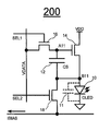
도 1은 본 발명의 실시예에 따른 픽셀 회로(200)를 도시한다. 픽셀 회로(200)는 아래에서 설명되는 바와 같은 CBVP 구동 방식을 채용한다. 도 1의 픽셀 회로(200)는 OLED(10), 스토리지 커패시터(12), 구동 트랜지스터(14), 및 스위치 트랜지스터(16 및 18)를 포함한다. 각각의 트랜지스터는 게이트 단자, 제1 단자 및 제2 단자를 갖는다. 본 명세서에서, "제1 단자"("제2 단자")는 드레인 단자 또는 소스 단자(소스 단자 또는 드레인 단자)일 수 있지만, 이에 한정되는 것은 아니다. 1 illustrates a
트랜지스터(14, 16 및 18)는 n형 TFT 트랜지스터이다. 픽셀 회로(200)에 적용되는 구동 기술은 또한 도 5에 도시된 바와 같은 p형 트랜지스터를 갖는 상보형(complementary) 픽셀 회로에도 적용 가능하다. The
트랜지스터(14, 16 및 18)는 비정질 실리콘, 나노/마이크로 결정질 실리콘, 폴리 실리콘, 유기 반도체 기술(예를 들어, 유기 TFT), NMOS 기술, 또는 CMOS 기술(예를 들어, MOSFET)을 사용하여 제조될 수 있다. 복수의 픽셀 회로(200)가 AMOLED 디스플레이 어레이를 형성할 수 있다.
2개의 선택 라인 SEL1 및 SEL2, 신호 라인 VDATA, 바이어스 라인 IBIAS, 전압 공급 라인 VDD, 및 공통 접지(common ground)가 픽셀 회로(200)에 제공된다. 도 1에서, 공통 접지는 OLED 상부 전극을 위한 것이다. 공통 접지는 픽셀 회로의 일부가 아니며, OLED(10)가 형성될 때 최종 단계에 형성된다. Two select lines SEL1 and SEL2, signal line VDATA, bias line IBIAS, voltage supply line VDD, and common ground are provided to
구동 트랜지스터(14)의 제1 단자는 전압 공급 라인 VDD에 접속된다. 구동 트랜지스터(14)의 제2 단자는 OLED(10)의 애노드 전극에 접속된다. 구동 트랜지스터(14)의 게이트 단자는 스위치 트랜지스터(16)를 통하여 신호 라인 VDATA에 접속된다. 스토리지 커패시터(12)는 구동 트랜지스터(14)의 제2 단자와 게이트 단자 사이에 접속된다. The first terminal of the
스위치 트랜지스터(16)의 게이트 단자는 제1 선택 라인 SEL1에 접속된다. 스위치 트랜지스터(16)의 제1 단자는 신호 라인 VDATA에 접속된다. 스위치 트랜지스터(16)의 제2 단자는 구동 트랜지스터(14)의 게이트 단자에 접속된다. The gate terminal of the
스위치 트랜지스터(18)의 게이트 단자는 제2 선택 라인 SEL2에 접속된다. 트랜지스터(18)의 제1 단자는 OLED(10)의 애노드 전극 및 스토리지 커패시터(12)에 접속된다. 스위치 트랜지스터(18)의 제2 단자는 바이어스 라인 IBIAS에 접속된다. OLED(10)의 캐소드 전극은 공통 접지에 접속된다. The gate terminal of the
트랜지스터(14 및 16) 및 스토리지 커패시터(12)는 노드 A11에 접속된다. OLED(10), 스토리지 커패시터(12) 및 트랜지스터(14 및 18)는 B11에 접속된다.
픽셀 회로(200)의 동작은 복수의 프로그래밍 사이클을 갖는 프로그래밍 단계 및 하나의 구동 사이클을 갖는 구동 단계를 포함한다. 프로그래밍 단계 동안, 노드 B11은 구동 트랜지스터(14)의 문턱 전압의 음(negative)으로 대전되고, 노드 A11은 프로그래밍 전압 VP로 대전된다. The operation of the
그 결과, 구동 트랜지스터(14)의 게이트-소스 전압은:As a result, the gate-source voltage of the
![]()
![]()
이며, 여기에서 VGS는 구동 트랜지스터(14)의 게이트-소스 전압을 나타내고, VT는 구동 트랜지스터(14)의 문턱 전압을 나타낸다. 이 전압은 구동 단계에서 커패시터(12)를 온(on) 상태로 유지시키며, 그 결과 구동 단계에서 OLED(10)를 통해 원하는 전류의 흐름을 일으킨다. Where VGS represents the gate-source voltage of the
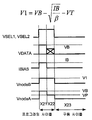
픽셀 회로(200)의 프로그래밍 및 구동 단계에 대해 상세하게 기재된다. 도 2는 도 1의 픽셀 회로(200)에 적용되는 하나의 예시적인 동작 프로세스를 예시한다. 도 2에서, VnodeB는 노드 B11의 전압을 나타내고, VnodeA는 노드 A11의 전압을 나타낸다. 도 2에 도시된 바와 같이, 프로그래밍 단계는 2개의 동작 사이클 X11, X12를 가지며, 구동 단계는 하나의 동작 사이클 X13을 갖는다. The programming and driving steps of the
제1 동작 사이클 X11: 선택 라인 SEL1과 SEL2 둘 다 하이(high)이다. 바이어스 전류 IB는 바이어스 라인 IBIAS를 통하여 흐르고, VDATA는 바이어스 전압 VB로 간다. First Operation Cycle X11: Both selection lines SEL1 and SEL2 are high. Bias current IB flows through bias line IBIAS and VDATA goes to bias voltage VB.
그 결과, 노드 B11의 전압은: As a result, the voltage at node B11 is:

이며, 여기에서 VnodeB는 노드 B11의 전압을 나타내고, VT는 구동 트랜지스터(14)의 문턱 전압을 나타내고, ![]()
![]()
![]()
![]()
제2 동작 사이클 X12: SEL2가 로우(low)이고 SEL1이 하이인 동안, VDATA가 프로그래밍 전압 VP로 간다. OLED(20)의 커패시턴스(11)가 크기 때문에, 이전 사이클에서 발생된 노드 B11의 전압은 그대로 유지된다. Second Operation Cycle X12: While SEL2 is low and SEL1 is high, VDATA goes to the programming voltage VP. Since the
따라서, 구동 트랜지스터(14)의 게이트-소스 전압을 다음과 같이 알 수 있다: Thus, the gate-source voltage of the
![]()
![]()

(4)에 기초하여 VB가 적절하게 선택될 때 △VB는 0이다. 구동 트랜지스터(14)의 게이트-소스 전압, 즉 VP+VT가 스토리지 커패시터(12)에 저장된다. When VB is appropriately selected based on (4), ΔVB is zero. The gate-source voltage of the driving
제3 동작 사이클 X13: IBIAS가 로우로 간다. SEL1은 0으로 간다. 스토리지 커패시터(12)에 저장된 전압이 구동 트랜지스터(14)의 게이트 단자에 인가된다. 구동 트랜지스터(14)는 온이다. 구동 트랜지스터(14)의 게이트-소스 전압은 스토리지 커패시터(12)에 저장된 전압 이상을 낸다. 따라서, OLED(10)를 통한 전류는 구동 트랜지스터(14)의 문턱 전압의 시프트 및 OLED 특성에 관계없어진다. Third operating cycle X13: IBIAS goes low. SEL1 goes to zero. The voltage stored in the
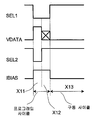
도 3은 도 1의 픽셀 회로(200)에 적용되는 부가의 예시적인 동작 프로세스를 예시한다. 도 3에서, VnodeB는 노드 B11의 전압을 나타내고, VnodeA는 노드 A11의 전압을 나타낸다. 3 illustrates an additional exemplary operating process applied to the
프로그래밍 단계는 2개의 동작 사이클 X21, X22을 갖고, 구동 단계는 하나의 동작 사이클 X23을 갖는다. 제1 동작 사이클 X21은 도 2의 제1 동작 사이클 X11과 동일하다. 제3 동작 사이클 X33은 도 2의 제3 동작 사이클 X13과 동일하다. 도 3에서, 선택 라인 SEL1 및 SEL2는 동일한 타이밍을 갖는다. 따라서, SEL1 및 SEL2는 공통 선택 라인에 접속될 수 있다. The programming stage has two operating cycles X21, X22 and the driving stage has one operating cycle X23. The first operating cycle X21 is the same as the first operating cycle X11 of FIG. 2. The third operation cycle X33 is the same as the third operation cycle X13 of FIG. 2. In Fig. 3, the selection lines SEL1 and SEL2 have the same timing. Thus, SEL1 and SEL2 can be connected to a common select line.
제2 동작 사이클 X22: SEL1 및 SEL2는 하이이다. 스위치 트랜지스터(18)는 온이다. IBIAS를 통해 흐르는 바이어스 전류 IB는 0이다. Second operating cycle X22: SEL1 and SEL2 are high. The
구동 트랜지스터(14)의 게이트-소스 전압은 상기 기재한 바와 같이 VGS=VP+VT일 수 있다. 구동 트랜지스터(14)의 게이트-소스 전압, 즉 VP+VT는 스토리지 커패시터(12)에 저장된다. The gate-source voltage of the
도 4는 도 1의 픽셀 회로(200)에 대한 시뮬레이션 결과 및 도 2의 파형을 도시한다. 결과에는, 대부분의 프로그래밍 전압에 대하여, 구동 트랜지스터(예를 들어, 도 1의 14)의 2V VT-시프트로 인한 OLED 전류의 변화가 거의 0 퍼센트임을 보여준다. 문턱 전압과 같은 시뮬레이션 파라미터는, 낮은 프로그래밍 전압에서 시프트가 높은 비율을 가짐을 보여준다. 4 illustrates simulation results for the
도 5는 p형 트랜지스터를 갖는 픽셀 회로(202)를 도시한다. 픽셀 회로(202)는 도 1의 픽셀 회로(200)에 대응한다. 픽셀 회로(202)는 도 6 및 도 7에 도시된 바와 같은 CBVP 구동 방식을 채용한다. 픽셀 회로(202)는 OLED(20), 스토리지 커패시터(22), 구동 트랜지스터(24), 및 스위치 트랜지스터(26 및 28)를 포함한다. 트랜지스터(24, 26 및 28)는 p형 트랜지스터이다. 각각의 트랜지스터는 게이트 단자, 제1 단자 및 제2 단자를 갖는다. 5 shows a
트랜지스터(24, 26 및 28)는 비정질 실리콘, 나노/마이크로 결정질 실리콘, 폴리 실리콘, 유기 반도체 기술(예를 들어, 유기 TFT), PMOS 기술, 또는 CMOS 기술(예를 들어, MOSFET)을 사용하여 제조될 수 있다. 복수의 픽셀 회로(202)가 AMOLED 디스플레이 어레이를 형성할 수 있다.
2개의 선택 라인 SEL1 및 SEL2, 신호 라인 VDATA, 바이어스 라인 IBIAS, 전압 공급 라인 VDD, 및 공통 접지가 픽셀 회로(202)에 제공된다. Two select lines SEL1 and SEL2, signal line VDATA, bias line IBIAS, voltage supply line VDD, and common ground are provided to the
트랜지스터(24 및 26) 및 스토리지 커패시터(22)는 노드 A12에 접속된다. OLED(20)의 캐소드 전극, 스토리지 커패시터(22) 및 트랜지스터(24 및 28)는 B12에 접속된다. OLED 캐소드가 픽셀 회로(202)의 다른 소자들에 접속되므로, 이는 임의의 OLED 제조와의 집적을 보장한다.
도 6은 도 5의 픽셀 회로(202)에 적용되는 하나의 예시적인 동작 프로세스를 예시한다. 도 6은 도 2에 대응한다. 도 7은 도 5의 픽셀 회로(202)에 적용되는 부가의 예시적인 동작 프로세스를 예시한다. 도 7은 도 3에 대응한다. 도 6 및 도 7의 CBVP 구동 방식은 도 2 및 도 3의 IBIAS 및 VDATA와 유사한 IBIAS 및 VDATA를 사용한다. 6 illustrates one example operational process applied to the
도 8은 본 발명의 실시예에 따른 픽셀 회로(204)를 도시한다. 픽셀 회로(204)는 상기 기재한 바와 같은 CBVP 구동 방식을 채용한다. 도 8의 픽셀 회로(204)는 OLED(30), 스토리지 커패시터(32 및 33), 구동 트랜지스터(34), 및 스위치 트랜지스터(36, 38 및 40)를 포함한다. 각각의 트랜지스터(34, 35 및 36)는 게이트 단자, 제1 단자 및 제2 단자를 포함한다. 이 픽셀 회로(204)는 픽셀 회로(200)의 방식과 동일한 방식으로 동작한다. 8 illustrates a
트랜지스터(34, 36, 38 및 40)는 n형 TFT 트랜지스터이다. 픽셀 회로(204)에 적용되는 구동 기술은 도 10에 도시된 바와 같은 p형 트랜지스터를 갖는 상보형 픽셀 회로에도 적용 가능하다. The
트랜지스터(34, 36, 38 및 40)는 비정질 실리콘, 나노/마이크로 결정질 실리콘, 폴리 실리콘, 유기 반도체 기술(예를 들어, 유기 TFT), NMOS 기술, 또는 CMOS 기술(예를 들어, MOSFET)을 사용하여 제조될 수 있다. 복수의 픽셀 회로(204)가 AMOLED 디스플레이 어레이를 형성할 수 있다.
선택 라인 SEL, 신호 라인 VDATA, 바이어스 라인 IBIAS, 전압 라인 VDD, 및 공통 접지가 픽셀 회로(204)에 제공된다. Select line SEL, signal line VDATA, bias line IBIAS, voltage line VDD, and common ground are provided to
구동 트랜지스터(34)의 제1 단자는 OLED(30)의 캐소드 전극에 접속된다. 구동 트랜지스터(34)의 제2 단자는 접지에 접속된다. 구동 트랜지스터(34)의 게이트 단자는 스위치 트랜지스터(36)를 통하여 그의 제1 단자에 접속된다. 스토리지 커패시터(32 및 33)는 직렬로 이루어지며, 구동 트랜지스터(34)의 게이트와 접지 사이에 접속된다. The first terminal of the driving
스위치 트랜지스터(36)의 게이트 단자는 선택 라인 SEL에 접속된다. 스위치 트랜지스터(36)의 제1 단자는 구동 트랜지스터(34)의 제1 단자에 접속된다. 스위치 트랜지스터(36)의 제2 단자는 구동 트랜지스터(34)의 게이트 단자에 접속된다. The gate terminal of the
스위치 트랜지스터(38)의 게이트 단자는 선택 라인 SEL에 접속된다. 스위치 트랜지스터(38)의 제1 단자는 신호 라인 VDATA에 접속된다. 스위치 트랜지스터(38)의 제2 단자는 스토리지 커패시터(32 및 33)의 접속 단자(즉, 노드 C21)에 접속된다. The gate terminal of the
스위치 트랜지스터(40)의 게이트 단자는 선택 라인 SEL에 접속된다. 스위치 트랜지스터(40)의 제1 단자는 바이어스 라인 IBIAS에 접속된다. 스위치 트랜지스터(40)의 제2 단자는 OLED(30)의 캐소드 단자에 접속된다. OLED(30)의 애노드 전극은 VDD에 접속된다. The gate terminal of the
OLED(30), 트랜지스터(34, 36, 및 40)는 노드 A21에서 접속된다. 스토리지 커패시터(32) 및 트랜지스터(34 및 36)는 노드 B21에서 접속된다.
픽셀 회로(204)의 동작은 복수의 프로그래밍 사이클을 갖는 프로그래밍 단계, 및 하나의 구동 사이클을 갖는 구동 단계를 포함한다. 프로그래밍 단계 동안, 제1 스토리지 커패시터(32)는 구동 트랜지스터(34)의 문턱 전압에 프로그래밍 전압 VP를 더한 값으로 대전되며, 제2 스토리지 커패시터(33)는 0으로 대전된다. The operation of
그 결과, 구동 트랜지스터(34)의 게이트-소스 전압은: As a result, the gate-source voltage of the
![]()
![]()
이며, 여기에서 VGS는 구동 트랜지스터(34)의 게이트-소스 전압을 나타내고, VT는 구동 트랜지스터(34)의 문턱 전압을 나타낸다. Where VGS represents the gate-source voltage of the
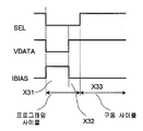
픽셀 회로(204)의 프로그래밍 및 구동 단계에 대해 상세하게 기재된다. 도 9는 도 8의 픽셀 회로(204)에 적용되는 하나의 예시적인 동작 프로세스를 예시한다. 도 9에 도시된 바와 같이, 프로그래밍 단계는 2개의 동작 사이클 X31, X32를 가지며, 구동 단계는 하나의 동작 사이클 X33을 갖는다. The programming and driving steps of the
제1 동작 사이클 X31: 선택 라인 SEL은 하이이다. 바이어스 전류 IB는 바이어스 라인 IBIAS를 통해 흐르고, VDATA는 VB-VP로 가며, 여기에서 VP는 프로그래밍 전압이고 VB는 다음에 의해 주어진다: First operation cycle X31: The selection line SEL is high. Bias current IB flows through bias line IBIAS, VDATA goes to VB-VP, where VP is the programming voltage and VB is given by:

그 결과, 제1 커패시터(32)에 저장된 전압은:As a result, the voltage stored in the first capacitance? (32) is:
![]()
![]()
이며, 여기에서 VC1은 제1 스토리지 커패시터(32)에 저장된 전압을 나타내고, VT는 구동 트랜지스터(34)의 문턱 전압을 나타내며, ![]()
![]()
![]()
![]()
제2 동작 사이클: SEL이 하이인 동안, VDATA는 0이고, IBIAS는 0으로 간다. OLED(30)의 커패시턴스(31)와 바이어스 라인 IBIAS의 기생 커패시턴스가 크기 때문에, 이전 사이클에서 발생된 노드 B21의 전압 및 노드 A21의 전압은 변하지 않은 채 유지된다. Second operating cycle: While SEL is high, VDATA is zero and IBIAS goes to zero. Since the
따라서, 구동 트랜지스터(34)의 게이트-소스 전압을 다음과 같이 알 수 있다: Thus, the gate-source voltage of the
![]()
![]()
여기에서, VGS는 구동 트랜지스터(34)의 게이트-소스 전압을 나타낸다. Here, VGS represents the gate-source voltage of the
구동 트랜지스터(34)의 게이트-소스 전압은 스토리지 커패시터(32)에 저장된다. The gate-source voltage of the driving
제3 동작 사이클 X33: IBIAS는 0으로 간다. SEL은 0으로 간다. 노드 C21의 전압은 0으로 간다. 스토리지 커패시터(32)에 저장된 전압은 구동 트랜지스터(34)의 게이트 단자에 인가된다. 구동 트랜지스터(34)의 게이트-소스 전압은 스토리지 커패시터(32)에 저장된 전압 이상을 낸다. 구동 트랜지스터(34)의 전류가 주로 그의 게이트-소스 전압에 의해 정의된다는 것을 고려하면, OLED(30)를 통한 전류는 구동 트랜지스터(34)의 문턱 전압의 시프트 및 OLED 특성에 관계없어진다. Third operating cycle X33: IBIAS goes to zero. SEL goes to zero. The voltage at node C21 goes to zero. The voltage stored in the
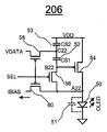
도 10은 p형 트랜지스터를 갖는 픽셀 회로(206)를 도시한다. 픽셀 회로(206)는 도 8의 픽셀 회로(204)에 대응한다. 픽셀 회로(206)는 도 11에 도시된 바와 같은 CBVP 구동 방식을 채용한다. 도 10의 픽셀 회로(206)는 OLED(50), 스토리지 커패시터(52 및 53), 구동 트랜지스터(54), 및 스위치 트랜지스터(56, 58, 및 60)를 포함한다. 트랜지스터(54, 56, 58 및 60)는 p형 트랜지스터이다. 각각의 트랜지스터는 게이트 단자, 제1 단자 및 제2 단자를 갖는다. 10 shows a
트랜지스터(54, 56, 58 및 60)는 비정질 실리콘, 나노/마이크로 결정질 실리콘, 폴리 실리콘, 유기 반도체 기술(예를 들어, 유기 TFT), PMOS 기술, 또는 CMOS 기술(예를 들어, MOSFET)을 사용하여 제조될 수 있다. 복수의 픽셀 회로(206)가 AMOLED 디스플레이 어레이를 형성할 수 있다.
2개의 선택 라인 SEL1 및 SEL2, 단일 라인 VDATA, 바이어스 라인 IBIAS, 전압 공급 라인 VDD, 및 공통 접지가 픽셀 회로(206)에 제공된다. 공통 접지는 도 1의 공통 접지와 동일한 것일 수 있다. Two select lines SEL1 and SEL2, single line VDATA, bias line IBIAS, voltage supply line VDD, and common ground are provided to the
OLED(50)의 애노드 전극, 트랜지스터(54, 56, 및 60)는 노드 A22에서 접속된다. 스토리지 커패시터(52) 및 트랜지스터(54 및 56)는 노드 B22에서 접속된다. 스위치 트랜지스터(58), 및 스토리지 커패시터(52 및 53)는 노드 C22에서 접속된다. The anode electrode,
도 11은 도 10의 픽셀 회로(206)에 적용되는 하나의 예시적인 동작 프로세스를 예시한다. 도 11은 도 9에 대응한다. 도 11에 도시된 바와 같이, 도 11의 CBVP 구동 방식은 도 9의 IBIAS 및 VDATA와 유사한 IBIAS 및 VDATA를 사용한다. FIG. 11 illustrates one exemplary operational process applied to the
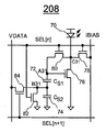
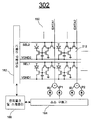
도 12는 본 발명의 실시예에 따른 디스플레이(208)를 도시한다. 디스플레이(208)는 아래에 기재된 바와 같은 CBVP 구동 방식을 채용한다. 도 12에서, 2개의 행 및 1개의 열과 연관된 소자가 예로서 도시되어 있다. 디스플레이(208)는 2개보다 많은 수의 행 및 1개보다 많은 수의 열을 포함할 수 있다. 12 shows a
디스플레이(208)는 OLED(70), 스토리지 커패시터(72 및 73), 트랜지스터(76, 78, 80, 82, 및 84)를 포함한다. 트랜지스터(76)는 구동 트랜지스터이다. 트랜지스터(78, 80, 및 84)는 스위치 트랜지스터이다. 각각의 트랜지스터(76, 78, 80, 82 및 84)는 게이트 단자, 제1 단자 및 제2 단자를 포함한다.
트랜지스터(76, 78, 80, 82 및 84)는 n형 TFT 트랜지스터이다. 픽셀 회로(208)에 적용되는 구동 기술은 도 16에 도시된 바와 같은 p형 트랜지스터를 갖는 상보형 픽셀 회로에도 적용 가능하다. The
트랜지스터(76, 78, 80, 82 및 84)는 비정질 실리콘, 나노/마이크로 결정질 실리콘, 폴리 실리콘, 유기 반도체 기술(예를 들어, 유기 TFT), NMOS 기술, 또는 CMOS 기술(예를 들어, MOSFET)을 사용하여 제조될 수 있다. 디스플레이(208)는 AMOLED 디스플레이 어레이를 형성할 수 있다. CBVP 구동 방식과 디스플레이(208)의 조합은 대면적 고해상도 AMOLED 디스플레이를 제공한다.
트랜지스터(76 및 80)와 스토리지 커패시터(72)는 노드 A31에서 접속된다. 트랜지스터(82 및 84)와 스토리지 커패시터(72 및 74)는 B31에서 접속된다.
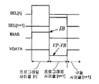
도 13은 도 12의 디스플레이(208)에 적용되는 하나의 예시적인 동작 프로세스를 예시한다. 도 13에서, "프로그래밍 사이클[n]"은 디스플레이(208)의 행 [n]에 대한 프로그래밍 사이클을 나타낸다. FIG. 13 illustrates one example operational process applied to the
2개의 연속하는 행들(n과 n+1) 사이에 프로그래밍 시간이 공유된다. n번째 행의 프로그래밍 사이클 동안, SEL[n]은 하이이고, 바이어스 전류 IB는 트랜지스터(78 및 80)를 통하여 흐르고 있다. 노드 A31에서의 전압은, 노드 B31에서의 전압이 0인 동안, ![]()
![]()
![]()
![]()
![]()
![]()
![]()
![]()
(n+1)번째 행의 프로그래밍 사이클 동안, VDATA는 VP-VB로 변한다. 그 결과, 노드 A31에서의 전압은 ![]()
![]()
![]()
![]()
다양한 바이어스 전류에 대하여 CBVP 픽셀 회로의 정착 시간이 도 14에 나타나 있다. 여기에서는 작은 전류가 IB로서 사용될 수 있으며, 그 결과 전력 소모가 적어진다. The settling times of the CBVP pixel circuits for various bias currents are shown in FIG. 14. Here a small current can be used as IB, resulting in lower power consumption.
도 15는 CBVP 픽셀 회로의 I-V 특성 뿐만 아니라, 구동 트랜지스터(예를 들어, 도 12의 76)의 문턱 전압의 2-V 시프트로 인해 픽셀 전류에 유도된 총 오류를 도시한다. 결과는 픽셀 전류에 있어서 2% 미만의 총 오류를 나타낸다. ![]()
![]()
도 16은 p형 트랜지스터를 갖는 디스플레이(210)를 도시한다. 디스플레이(210)는 도 12의 디스플레이(208)에 대응한다. 디스플레이(210)는 도 17에 도시된 바와 같은 CBVP 구동 방식을 채용한다. 도 12에서, 2개의 행 및 1개의 열과 연관된 소자가 예로서 도시되어 있다. 디스플레이(210)는 2개보다 많은 수의 행 및 1개보다 많은 수의 열을 포함할 수 있다. 16 shows a
디스플레이(210)는 OLED(90), 스토리지 커패시터(92, 및 94), 및 트랜지스터(96, 98, 100, 102 및 104)를 포함한다. 트랜지스터(96)는 구동 트랜지스터이다. 트랜지스터(100 및 104)는 스위치 트랜지스터이다. 트랜지스터(24, 26 및 28)는 p형 트랜지스터이다. 각각의 트랜지스터는 게이트 단자, 제1 단자 및 제2 단자를 갖는다.
트랜지스터(96, 98, 100, 102, 및 104)는 비정질 실리콘, 나노/마이크로 결정질 실리콘, 폴리 실리콘, 유기 반도체 기술(예를 들어, 유기 TFT), PMOS 기술, 또는 CMOS 기술(예를 들어, MOSFET)을 사용하여 제조될 수 있다. 디스플레이(210)는 AMOLED 디스플레이 어레이를 형성할 수 있다.
도 16에서, 구동 트랜지스터(96)는 OLED(90)의 애노드 전극과 전압 공급 라인 VDD 사이에 접속된다. In FIG. 16, the
도 17은 도 16의 디스플레이(210)에 적용되는 하나의 예시적인 동작 프로세스를 예시한다. 도 17은 도 13에 대응한다. 도 17의 CBVP 구동 방식은 도 13의 IBIAS 및 VDATA와 유사한 IBIAS 및 VDATA를 사용한다. 17 illustrates one example operational process applied to the
CBVP 구동 방식에 따라, 그의 문턱 전압 및 OLED 전압과 무관하도록 구동 트랜지스터에 제공된 오버드라이브(overdrive) 전압이 발생된다. According to the CBVP driving scheme, an overdrive voltage provided to the driving transistor is generated to be independent of its threshold voltage and the OLED voltage.
픽셀 소자(들)의 특성(들)의 시프트(들)(예를 들어, 연장된 디스플레이 동작 하의 발광 소자의 열화 및 구동 트랜지스터의 문턱 전압 시프트)는, 스토리지 커패시터에 저장된 전압에 의해 그리고 그것을 구동 트랜지스터의 게이트에 인가함으로써, 보상된다. 따라서, 픽셀 회로는 시프트의 어떠한 영향 없이 발광 소자를 통하여 안정적인 전류를 제공할 수 있으며, 이는 디스플레이 동작 수명을 향상시킨다. 또한, 회로 단순성으로 인해, 종래의 픽셀 회로보다 더 높은 생산 수율, 더 적은 제조 비용 및 더 높은 해상도를 보장한다. The shift (s) of the characteristic (s) of the pixel element (s) (e.g., degradation of the light emitting element under extended display operation and threshold voltage shift of the driving transistor) is driven by the voltage stored in the storage capacitor and the driving transistor thereof. By applying to the gate of is compensated. Thus, the pixel circuit can provide a stable current through the light emitting element without any influence of the shift, which improves the display operating life. In addition, the circuit simplicity ensures higher production yields, lower manufacturing costs and higher resolutions than conventional pixel circuits.
상기 기재된 픽셀 회로의 정착 시간은 종래의 픽셀 회로보다 훨씬 더 작으므로, 고해상도 TV와 같은 대면적 디스플레이에 적합하지만, 이는 또한 소형 디스플레이 면적을 배제하는 것은 아니다. Since the settling time of the pixel circuit described above is much smaller than the conventional pixel circuit, it is suitable for large area displays such as high resolution TVs, but this also does not exclude a small display area.
CBVP 픽셀 회로(예를 들어, 200, 202 또는 204)를 갖는 디스플레이 어레이를 구동하기 위한 구동기는 픽셀 휘도 데이터를 전압으로 변환한다는 것을 유의한다. Note that a driver for driving a display array having a CBVP pixel circuit (eg, 200, 202 or 204) converts pixel luminance data into voltage.
이제 전압 바이어싱된 전류 프로그래밍된(VBCP; voltage-biased current-programmed) 구동 방식을 포함하는 픽셀에 대한 구동 기술이 상세하게 기재된다. VBCP 구동 방식에서, 미러 트랜지스터를 리사이징하지 않고 픽셀 전류가 스케일링 다운된다. VBCP 구동 방식은 전류를 사용하여 다양한 그레이 스케일을 제공하고(전류 프로그래밍), 바이어스를 사용하여 프로그래밍을 가속화하고 문턱 전압 시프트와 같은 픽셀의 시간 의존적 파라미터를 보상한다. 구동 트랜지스터의 단자들 중 하나는 가상 접지(virtual ground) VGND에 접속된다. 가상 접지의 전압을 변경함으로써, 픽셀 전류가 변경된다. 바이어스 전류 IB는 구동기측에서 프로그래밍 전류 IP에 더해지고, 그 다음 가상 접지의 전압을 변경함으로써 픽셀 회로로의 프로그래밍 전류로부터 바이어스 전류가 제거된다. The driving technique for pixels including a voltage-biased current-programmed (VBCP) driving scheme is now described in detail. In the VBCP driving scheme, the pixel current is scaled down without resizing the mirror transistor. The VBCP driving scheme uses current to provide various gray scales (current programming), biasing to accelerate programming and compensate for pixel's time dependent parameters such as threshold voltage shifts. One of the terminals of the driving transistor is connected to a virtual ground VGND. By changing the voltage of the virtual ground, the pixel current is changed. The bias current IB is added to the programming current IP at the driver side, and then the bias current is removed from the programming current into the pixel circuit by changing the voltage of the virtual ground.
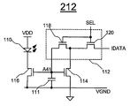
도 18은 본 발명의 부가적인 실시예에 따른 픽셀 회로(212)를 도시한다. 픽셀 회로(212)는 상기 기재한 바와 같은 VBCP 구동 방식을 채용한다. 도 18의 픽셀 회로(212)는 OLED(110), 스토리지 커패시터(111), 스위치 네트워크(112) 및 미러 트랜지스터(114 및 116)를 포함한다. 미러 트랜지스터(114 및 116)는 전류 미러를 형성한다. 트랜지스터(114)는 프로그래밍 트랜지스터이다. 트랜지스터(116)는 구동 트랜지스터이다. 스위치 네트워크(112)는 스위치 트랜지스터(118 및 120)를 포함한다. 각각의 트랜지스터(114, 116, 118 및 120)는 게이트 단자, 제1 단자 및 제2 단자를 갖는다. 18 illustrates a
트랜지스터(114, 116, 118 및 120)는 n형 TFT 트랜지스터이다. 픽셀 회로(212)에 적용된 구동 기술은 또한 도 20에 도시된 바와 같은 p형 트랜지스터를 갖는 상보형 픽셀 회로에도 적용 가능하다.
트랜지스터(114, 116, 118 및 120)는 비정질 실리콘, 나노/마이크로 결정질 실리콘, 폴리 실리콘, 유기 반도체 기술(예를 들어, 유기 TFT), NMOS 기술, 또는 CMOS 기술(예를 들어, MOSFET)을 사용하여 제조될 수 있다. 복수의 픽셀 회로(212)가 AMOLED 디스플레이 어레이를 형성할 수 있다.
선택 라인 SEL, 신호 라인 IDATA, 가상 접지 라인 VGND, 전압 공급 라인 VDD, 및 공통 접지가 픽셀 회로(150)에 제공된다. Select line SEL, signal line IDATA, virtual ground line VGND, voltage supply line VDD, and common ground are provided to
트랜지스터(116)의 제1 단자는 OLED(110)의 캐소드 전극에 접속된다. 트랜지스터(116)의 제2 단자는 VGND에 접속된다. 트랜지스터(114)의 게이트 단자, 트랜지스터(116)의 게이트 단자, 및 스토리지 커패시터(111)는 접속 노드 A41에 접속된다. The first terminal of
스위치 트랜지스터(118 및 120)의 게이트 단자는 SEL에 접속된다. 스위치 트랜지스터(120)의 제1 단자는 IDATA에 접속된다. 스위치 트랜지스터(118 및 120)는 트랜지스터(114)의 제1 단자에 접속된다. 스위치 트랜지스터(118)는 노드 A41에 접속된다. Gate terminals of the
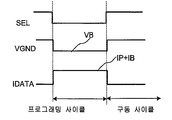
도 19는 도 18의 픽셀 회로(212)에 대한 예시적인 동작을 예시한다. 도 18 및 도 19를 참조하여, 픽셀 회로(212)에 적용되는 전류 스케일링 기술에 대해 상세하게 기재된다. 픽셀 회로(212)의 동작은 프로그래밍 사이클 X41, 및 구동 사이클 X42를 갖는다. FIG. 19 illustrates example operations for the
프로그래밍 사이클 X41: SEL은 하이이다. 따라서, 스위치 트랜지스터(118 및 120)는 온이다. VGND는 바이어스 전압 VB로 간다. 전류 (IB+IP)가 IDATA를 통하여 제공되며, 여기에서 IP는 프로그래밍 전류를 나타내고, IB는 바이어스 전류를 나타낸다. (IB+IP)와 동일한 전류가 스위치 트랜지스터(118 및 120)를 통과한다. Programming cycle X41: SEL is high. Thus, switch
구동 트랜지스터(116)의 게이트-소스 전압은 다음으로 자가 조정된다: The gate-source voltage of the

여기에서, VT는 구동 트랜지스터(116)의 문턱 전압을 나타내고, ![]()
![]()
![]()
![]()
스토리지 커패시터(111)에 저장된 전압은:The voltage stored on the

이며, 여기에서 VCS는 스토리지 커패시터(111)에 저장된 전압을 나타낸다. Where VCS represents the voltage stored in the
구동 트랜지스터(116)의 하나의 단자가 VGND에 접속되므로, 프로그래밍 시간 동안 OLED(110)를 통하여 흐르는 전류는: Since one terminal of the
![]()
![]()
이고, Ipixel은 OLED(110)를 통하여 흐르는 픽셀 전류를 나타낸다. Ipixel represents the pixel current flowing through the
IB >> IP인 경우, 픽셀 전류 Ipixel은 다음과 같이 쓸 수 있다: For IB >> IP, the pixel current Ipixel can be written as:
![]()
![]()
VB는 다음과 같이 적절하게 선택된다: VB is appropriately selected as follows:

픽셀 전류 Ipixel은 프로그래밍 전류 IP와 동일하게 된다. 따라서, 이는 프로그래밍 사이클 동안의 원치 않는 방출을 피한다. The pixel current Ipixel is equal to the programming current IP. Thus, this avoids unwanted emissions during programming cycles.
리사이징이 요구되지 않으므로, 전류-미러 픽셀 회로에서 2개의 미러 트랜지스터 사이의 보다 나은 정합을 얻을 수 있다. Since no resizing is required, better matching between the two mirror transistors in the current-mirror pixel circuit can be obtained.
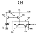
도 20은 p형 트랜지스터를 갖는 픽셀 회로(214)를 도시한다. 픽셀 회로(214)는 도 18의 픽셀 회로(212)에 대응한다. 픽셀 회로(214)는 도 21에 도시된 바와 같이 VBCP 구동 방식을 채용한다. 픽셀 회로(214)는 OLED(130), 스토리지 커패시터(131), 스위치 네트워크(132), 및 미러 트랜지스터(134 및 136)를 포함한다. 미러 트랜지스터(134 및 136)는 전류 미러를 형성한다. 트랜지스터(134)는 프로그래밍 트랜지스터이다. 트랜지스터(136)는 구동 트랜지스터이다. 스위치 네트워크(132)는 스위치 트랜지스터(138 및 140)를 포함한다. 트랜지스터(134, 136, 138 및 140)는 p형 TFT 트랜지스터이다. 각각의 트랜지스터(134, 136, 138 및 140)는 게이트 단자, 제1 단자, 및 제2 단자를 갖는다. 20 shows a
트랜지스터(134, 136, 138 및 140)는 비정질 실리콘, 나노/마이크로 결정질 실리콘, 폴리 실리콘, 유기 반도체 기술(예를 들어, 유기 TFT), PMOS 기술, 또는 CMOS 기술(예를 들어, MOSFET)을 사용하여 제조될 수 있다. 복수의 픽셀 회로(214)가 AMOLED 디스플레이 어레이를 형성할 수 있다.
선택 라인 SEL, 신호 라인 IDATA, 가상 접지 라인 VGND, 및 전압 공급 라인 VSS가 픽셀 회로(214)에 제공된다. Select line SEL, signal line IDATA, virtual ground line VGND, and voltage supply line VSS are provided to
트랜지스터(136)는 OLED(130)의 캐소드 전극와 VGND 사이에 접속된다. 트랜지스터(134)의 게이트 단자, 트랜지스터(136)의 게이트 단자, 스토리지 커패시터(131) 및 스위치 네트워크(132)는 노드 A42에서 접속된다.
도 21은 도 20의 픽셀 회로(214)에 대한 예시적인 동작을 예시한다. 도 21은 도 19에 대응한다. 도 21의 VBCP 구동 방식은 도 19의 IDATA 및 VGND와 유사한 IDATA 및 VGND를 사용한다. 21 illustrates example operations for the
픽셀 회로(212 및 214)에 적용된 VBCP 기술은 전류 미러 유형 픽셀 회로가 아닌 다른 전류 프로그래밍 픽셀 회로에 적용 가능하다. The VBCP technique applied to the
예를 들어, VBCP 기술은 AMOLED 디스플레이에 사용하기에 적합하다. VBCP 기술은 전류 프로그래밍된 픽셀 회로 디스플레이, 예를 들어 AMOLED 디스플레이의 정착 시간을 향상시킨다. For example, VBCP technology is suitable for use in AMOLED displays. VBCP technology improves the settling time of current programmed pixel circuit displays, such as AMOLED displays.
VBCP 픽셀 회로(예를 들어, 212, 214)를 갖는 디스플레이 어레이를 구동하기 위한 구동기는 픽셀 휘도 데이터를 전류로 변환한다는 것을 유의한다. Note that a driver for driving a display array having VBCP pixel circuits (eg, 212, 214) converts pixel luminance data into current.
도 22는 복수의 CBVP 픽셀 회로(151)(CBVP1-1, CBVP1-2, CBVP2-1, CBVP2-2)를 갖는 디스플레이 어레이(150)에 대한 구동 메커니즘을 도시한다. CBVP 픽셀 회로(151)는 CBVP 구동 방식이 적용 가능한 픽셀 회로이다. 예를 들어, CBVP 픽셀 회로(151)는 도 1, 도 5, 도 8, 도 10, 도 12, 또는 도 16에 도시된 픽셀 회로일 수 있다. 도 22에서, 4개의 CBVP 픽셀 회로(151)가 예로서 도시되어 있다. 디스플레이 어레이(150)는 4개보다 더 많거나 4개보다 더 적은 수의 CBVP 픽셀 회로(151)를 가질 수 있다. 22 shows a drive mechanism for
디스플레이 어레이(150)는 복수의 CBVP 픽셀 회로(151)가 행 및 열로 정렬되어 있는 AMOLED 디스플레이이다. 어레이 구조에서 공통 열 픽셀들 사이에 VDATA1(또는 VDATA2) 및 IBIAS1(또는 IBIAS2)가 공유되며, 공통 행 픽셀들 사이에 SEL1(또는 SEL2)이 공유된다. The
SEL1 및 SEL2는 어드레스 구동기(address driver)(152)를 통하여 구동된다. VDATA1 및 VDATA2는 소스 구동기(154)를 통하여 구동된다. IBIAS1 및 IBIAS2도 또한 소스 구동기(154)를 통하여 구동된다. 컨트롤러 및 스케쥴러(156)는 프로그래밍, 보정(calibration) 및 디스플레이 어레이를 동작시키기 위한 기타 동작의 제어 및 스케쥴링을 위해 제공되며, 이는 상기 기재한 바와 같은 CBVP 구동 방식에 대한 제어 및 스케쥴을 포함한다. SEL1 and SEL2 are driven through an
도 23은 복수의 VBCP 픽셀 회로를 갖는 디스플레이 어레이(160)에 대한 구동 메커니즘을 도시한다. 도 23에서, 도 18의 픽셀 회로(212)가 VBCP 픽셀 회로의 예로서 도시되어 있다. 그러나, 디스플레이 어레이(160)는 기재된 VBCP 구동 방식이 적용 가능한 임의의 기타 픽셀 회로를 포함할 수 있다. 23 illustrates a drive mechanism for
도 23의 SEL1 및 SEL2는 도 18의 SEL에 대응한다. 도 23의 VGND1 및 VGND2는 도 18의 VDATA에 대응한다. 도 23의 IDATA1 및 IDATA2는 도 18의 IDATA에 대응한다. 도 23에서, 4개의 VBCP 픽셀 회로가 예로서 도시되어 있다. 디스플레이 어레이(160)는 4개보다 더 많거나 4개보다 더 적은 수의 VBCP 픽셀 회로를 가질 수 있다. SEL1 and SEL2 in FIG. 23 correspond to SEL in FIG. 18. VGND1 and VGND2 in FIG. 23 correspond to VDATA in FIG. IDATA1 and IDATA2 in FIG. 23 correspond to IDATA in FIG. In FIG. 23, four VBCP pixel circuits are shown by way of example.
디스플레이 어레이(160)는 복수의 VBCP 픽셀 회로가 행 및 열로 정렬되어 있는 AMOLED 디스플레이이다. 어레이 구조에서 공통 열 픽셀들 사이에 IDATA1(또는 IDATA2)가 공유되며, 공통 행 픽셀들 사이에 SEL1(또는 SEL2) 또는 VGND1(또는 VGND2)이 공유된다.
SEL1, SEL2, VGND1 및 VGND2는 어드레스 구동기(162)를 통하여 구동된다. IDATA1 및 IDATA는 소스 구동기(164)를 통하여 구동된다. 컨트롤러 및 스케쥴러(166)는 프로그래밍, 보정 및 디스플레이 어레이를 동작시키기 위한 기타 동작의 제어 및 스케쥴링을 위해 제공되며, 이는 상기 기재한 바와 같은 VBCP 구동 방식에 대한 제어 및 스케쥴을 포함한다. SEL1, SEL2, VGND1, and VGND2 are driven through the
도 24는 본 발명의 부가적인 실시예에 따른 픽셀 회로(400)를 도시한다. 도 24의 픽셀 회로(400)는 3-TFT 전류 바이어싱된 전압 프로그래밍된 픽셀 회로이며, CBVP 구동 방식을 채용한다. 구동 방식은 부정합을 보상함으로써 디스플레이 수명 및 수율을 개선한다. 24 illustrates a
픽셀 회로(400)는 OLED(402), 스토리지 커패시터(404), 구동 트랜지스터(406), 및 스위치 트랜지스터(408 및 410)를 포함한다. 각각의 트랜지스터는 게이트 단자, 제1 단자 및 제2 단자를 갖는다. 트랜지스터(406, 408, 및 410)는 p형 TFT 트랜지스터이다. 픽셀 회로(400)에 적용된 구동 기술은 또한, n형 트랜지스터를 가지며 당해 기술 분야에서의 통상의 지식을 가진 자가 이해할 상보형 픽셀 회로에 적용 가능하다. The
트랜지스터(406, 408 및 410)는 폴리 실리콘, 나노/마이크로(결정질) 실리콘, 비정질 실리콘, CMOS, 유기 반도체, 금속 유기 기술, 또는 이들의 조합을 사용하여 구현될 수 있다. 복수의 픽셀 회로(400)가 능동 매트릭스 어레이를 형성할 수 있다. 픽셀 회로(400)에 적용된 구동 방식은 능동 매트릭스 디스플레이에서의 시간 및 공간적 비균일성을 보상한다.
선택 라인 SEL, 신호 라인 Vdata, 바이어스 라인 Ibias, 및 전압 공급 라인 Vdd가 픽셀 회로(400)에 접속된다. 바이어스 라인 Ibias는 수명, 전력, 및 디바이스 성능과 균일성과 같은 디스플레이 사양에 기초하여 정의되는 바이어스 전류(Ibias)를 제공한다. The selection line SEL, the signal line Vdata, the bias line Ibias, and the voltage supply line Vdd are connected to the
구동 트랜지스터(406)의 제1 단자는 전압 공급 라인 Vdd에 접속된다. 구동 트랜지스터(406)의 제2 단자는 노드 B20에서 OLED(402)에 접속된다. 커패시터(404)의 하나의 단자는 신호 라인 Vdata에 접속되고, 커패시터(404)의 다른 단자는 노드 A20에서 구동 트랜지스터(406)의 게이트 단자에 접속된다. The first terminal of the
스위치 트랜지스터(408 및 410)의 게이트 단자는 선택 라인 SEL에 접속된다. 스위치 트랜지스터(408)는 노드 A20와 노드 B20 사이에 접속된다. 스위치 트랜지스터(410)는 노드 B20와 바이어스 라인 Ibias 사이에 접속된다. Gate terminals of the
픽셀 회로(400)에 대하여, 미리 결정된 고정된 전류(Ibias)가 트랜지스터(410)를 통해 제공되어 모든 공간 및 시간적 비균일성을 보상하고, 다양한 그레이 스케일에 요구되는 다양한 전류 레벨의 전류를 분배하는데 전압 프로그래밍이 사용된다. For
도 25에 도시된 바와 같이, 픽셀 회로(400)의 동작은 프로그래밍 단계 X61 및 구동 단계 X62를 포함한다. 도 25의 Vdata[j]는 도 24의 Vdd에 대응한다. 도 25의 Vp[k,j](k=1,2,...,n)는 Vdata[j] 상의 k 번째 프로그래밍 전압을 나타내며, 여기에서 "j"는 열 번호이다. As shown in FIG. 25, the operation of the
도 24 및 도 25를 참조하여, 프로그래밍 사이클 X61 동안, SEL은 로우이며, 그리하여 스위치 트랜지스터(408 및 410)는 온이다. 바이어스 전류 Ibias가 바이어스 라인 Ibias를 통하여 픽셀 회로(400)에 인가되고, 구동 트랜지스터(406)의 게이트 단자는 모든 전류가 구동 트랜지스터(406)의 소스-드레인을 통과할 수 있도록 자가 조정된다. 이 사이클에서, Vdata는 픽셀의 그레이 스케일에 관련된 프로그래밍 전압을 갖는다. 구동 사이클 X62 동안, 스위치 트랜지스터(408 및 410)는 오프(off)이고, 전류는 구동 트랜지스터(406) 및 OLED(402)를 통과한다. 24 and 25, during programming cycle X61, SEL is low, so switch
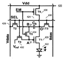
도 26은 본 발명의 부가적인 실시예에 따른 픽셀 회로(420)를 도시하는 도면이다. 도 26의 픽셀 회로(420)는 6-TFT 전류 바이어싱된 전압 프로그래밍된 픽셀 회로이며, 방출 제어(emission control)와 함께 CBVP 구동 방식을 채용한다. 이 구동 방식은 부정합을 보상함으로서 디스플레이 수명 및 수율을 개선한다. 26 is a diagram illustrating a
픽셀 회로(420)는 OLED(422), 스토리지 커패시터(424), 및 트랜지스터(426-436)를 포함한다. 각각의 트랜지스터는 게이트 단자, 제1 단자 및 제2 단자를 갖는다. 트랜지스터(426-436)는 p형 TFT 트랜지스터이다. 픽셀 회로(420)에 적용된 구동 기술은 또한, n형 트랜지스터를 가지며 당해 기술 분야에서의 통상의 지식을 가진 자라면 이해할 상보형 픽셀 회로에 적용 가능하다.
트랜지스터(426-436)는 폴리 실리콘, 나노/마이크로(결정질) 실리콘, 비정질 실리콘, CMOS, 유기 반도체, 금속 유기 기술, 또는 이들의 조합을 사용하여 구현될 수 있다. 복수의 픽셀 회로(420)가 능동 매트릭스 어레이를 형성할 수 있다. 픽셀 회로(420)에 적용된 구동 방식은 능동 매트릭스 어레이에서의 시간 및 공간적 비균일성을 보상한다. Transistors 426-436 may be implemented using polysilicon, nano / micro (crystalline) silicon, amorphous silicon, CMOS, organic semiconductors, metal organic technology, or a combination thereof. The plurality of
하나의 선택 라인 SEL, 신호 라인 Vdata, 바이어스 라인 Ibias, 전압 공급 라인 Vdd, 기준 전압 라인 Vref, 및 방출 신호 라인 EM이 픽셀 회로(420)에 접속된다. 바이어스 라인 Ibias는 수명, 전력 및 디바이스 성능과 균일성과 같은 디스플레이 사양에 기초하여 정의되는 바이어스 전류(Ibias)를 제공한다. 기준 전압 라인 Vref는 기준 전압(Vref)을 제공한다. 기준 전압 Vref는 그레이 스케일 및/또는 콘트라스트 비(contrast ratio)를 포함할 수 있는 디스플레이 사양 및 바이어스 전류 Ibias에 기초하여 결정될 수 있다. 신호 라인 EM은 픽셀 회로(420)를 온 시키는 방출 신호 EM을 제공한다. 픽셀 회로(420)는 방출 신호 EM에 기초하여 방출 모드로 간다. One select line SEL, signal line Vdata, bias line Ibias, voltage supply line Vdd, reference voltage line Vref, and emission signal line EM are connected to
트랜지스터(426)의 게이트 단자, 트랜지스터(432)의 하나의 단자, 및 트랜지스터(434)의 하나의 단자가 노드 A21에서 접속된다. 커패시터(424)의 하나의 단자, 트랜지스터(428)의 하나의 단자 및 트랜지스터(434)의 다른 단자가 노드 B21에서 접속된다. 커패시터(424)의 다른 단자, 트랜지스터(430)의 하나의 단자, 트랜지스터(436)의 하나의 단자, 및 트랜지스터(426)의 하나의 단자가 노드 C21에서 접속된다. 트랜지스터(430)의 다른 단자가 바이어스 라인 Ibias에 접속된다. 트랜지스터(432)의 다른 단자가 기준 전압 라인 Vref에 접속된다. 선택 라인 SEL은 트랜지스터(428, 430, 및 432)의 게이트 단자에 접속된다. 선택 라인 EM은 트랜지스터(434, 및 436)의 게이트 단자에 접속된다. 트랜지스터(426)는 구동 트랜지스터이다. 트랜지스터(428, 430, 432, 434 및 436)는 스위칭 트랜지스터이다. The gate terminal of
픽셀 회로(420)에 대하여, 미리 결정된 고정된 전류(Ibias)가 트랜지스터(430)를 통하여 제공되며, 기준 전압 Vref가 트랜지스터(426)의 게이트 단자에 트랜지스터(432)를 통해 인가되고, 프로그래밍 전압 VP가 스토리지 커패시터(424)의 다른 단자(즉, 노드 B21)에 트랜지스터(428)를 통해 인가된다. 여기에서, 트랜지스터(426)의 소스 전압(즉, 노드 C21의 전압)은 바이어스 전류가 트랜지스터(426)를 통해 갈 수 있도록 자가 조정될 것이며, 그리하여 모든 공간 및 시간적 비균일성을 보상한다. 또한, 다양한 그레이 스케일에 대해 요구되는 다양한 전류 레벨의 전류를 분배하는데 전압 프로그래밍이 사용된다. For
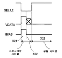
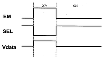
도 27에 도시된 바와 같이, 픽셀 회로(420)의 동작은 프로그래밍 단계 X71 및 구동 단계 X72를 포함한다. As shown in FIG. 27, the operation of the
도 26 및 도 27을 참조하면, 프로그래밍 사이클 X71 동안, SEL은 로우이며, 그리하여 트랜지스터(428, 430 및 432)는 온이고, 고정된 바이어스 전류가 Ibias 라인으로 인가되며, 트랜지스터(426)의 소스는 모든 전류가 트랜지스터(426)의 소스-드레인을 통과할 수 있도록 자가 조정된다. 이 사이클에서, Vdata는 픽셀의 그레이 스케일에 관련된 프로그래밍 전압을 갖고, 커패시터(424)는 프로그래밍 전압 및 부정합 보상을 위해 전류에 의해 발생된 전압을 저장한다. 구동 사이클 X72 동안, 트랜지스터(428, 430 및 432)는 오프이며, 트랜지스터(434 및 436)는 방출 신호 EM에 의해 온이다. 이 구동 사이클 X72 동안, 트랜지스터(426)는 OLED(422)에 대하여 전류를 제공한다. 26 and 27, during programming cycle X71, SEL is low, so
도 25에서는, 전체 디스플레이가 프로그래밍되고, 그 다음에 불이 켜진다(방출 모드로 감). 이와 대조적으로, 도 27에서는, 각각의 행이 방출 라인 EM을 사용함으로써 프로그래밍 후에 불이 켜질 수 있다. In Fig. 25, the entire display is programmed, then lit (going to emission mode). In contrast, in FIG. 27, each row can be lit after programming by using the emission line EM.
도 25 및 도 27의 동작에 있어서, 바이어스 라인은 미리 결정된 고정된 바이어스 전류를 제공한다. 그러나, 바이어스 전류 Ibias는 조정 가능할 수 있고, 바이어스 전류 Ibias는 디스플레이의 동작 동안 조정될 수 있다. In the operation of FIGS. 25 and 27, the bias line provides a predetermined fixed bias current. However, the bias current Ibias can be adjustable and the bias current Ibias can be adjusted during operation of the display.
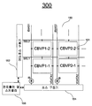
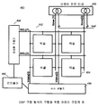
도 28은 CBVP 구동 방식의 구현을 위한 어레이 구조를 갖는 디스플레이 시스템의 예를 도시한다. 도 28의 디스플레이 시스템(450)은 복수의 픽셀(454)을 갖는 픽셀 어레이(452), 게이트 구동기(456), 소스 구동기(458) 및 구동기(456 및 458)를 제어하기 위한 컨트롤러(460)를 포함한다. 게이트 구동기(456)는 어드레스(선택) 라인(예를 들어, SEL[1], SEL[2]...)에 대해 동작한다. 소스 구동기(458)는 데이터 라인(예를 들어, Vdata[1], Vdata[2],...)에 대해 동작한다. 디스플레이 시스템(450)은 기준 전류 Iref를 사용하여 바이어스 라인(예를 들어, Ibias[1], Ibias[2])에 대해 동작하는 보정된 전류 미러 블록(462)을 포함한다. 블록(462)은 각각이 대응하는 Ibias에 대한 것인 복수의 보정된 전류 미러를 포함한다. 기준 전류 Iref는 보정된 전류 미러 블록(462)에 스위치를 통해 제공될 수 있다. 28 shows an example of a display system having an array structure for implementing the CBVP driving scheme. The
픽셀 회로(454)는 도 24의 픽셀 회로(400) 또는 도 26의 픽셀 회로(420)와 동일한 것일 수 있으며, 여기에서 SEL[i](i=1,2,...)는 도 24 또는 도 26의 SEL에 대응하고, Vdata[j](j=1,2,...)는 도 24 또는 도 26의 Vdata에 대응하고, Ibias[j](j=1,2,...)는 도 24 또는 도 26의 Ibias에 대응한다. 픽셀 회로(454)로서 도 26의 픽셀 회로(420)를 사용할 때, 게이트 구동기(456)와 같은 디스플레이의 주변 장치에서의 구동기는 각각의 방출 라인 EM을 제어한다. The
도 28에서, 전류 미러는 기준 전류 소스를 이용해 보정된다. 패널의 프로그래밍 사이클(예를 들어, 도 25의 X61, 도 27의 X71) 동안, 보정된 전류 미러(블록 462)는 바이어스 라인 Ibias에 전류를 제공한다. 이들 전류 미러는 패널의 에지에서 제조될 수 있다. In Fig. 28, the current mirror is corrected using the reference current source. During the programming cycle of the panel (eg, X61 in FIG. 25, X71 in FIG. 27), the corrected current mirror (block 462) provides current to the bias line Ibias. These current mirrors can be manufactured at the edge of the panel.
도 29는 CBVP 구동 방식의 구현을 위한 어레이 구조를 갖는 디스플레이 시스템의 다른 예를 도시한다. 도 29의 디스플레이 시스템(470)은 복수의 픽셀(474), 게이트 구동기(476), 소스 구동기(478), 및 구동기(476 및 478)를 제어하기 위한 컨트롤러(480)를 갖는 픽셀 어레이(472)를 포함한다. 게이트 구동기(476)는 어드레스(선택) 라인(예를 들어, SEL[0], SEL[1], SEL[2],...)에 대해 동작한다. 소스 구동기(478)는 데이터 라인(예를 들어, Vdata[1], Vdata[2],...)에 대해 동작한다. 디스플레이 시스템(470)은 Vdata 라인을 사용하여 바이어스 라인(예를 들어, Ibias[1], Ibias[2])에 대해 동작하기 위한 보정된 전류 소스 블록(482)을 포함한다. 블록(482)은 각각이 Ibias 라인에 대하여 제공되는 것인 복수의 보정된 전류 소스를 포함한다. 29 shows another example of a display system having an array structure for implementing a CBVP driving scheme. The
픽셀 회로(474)는 도 24의 픽셀 회로(400) 또는 도 26의 픽셀 회로(420)와 동일한 것일 수 있으며, 여기에서 SEL[i](i=1,2,...)은 도 24 또는 도 26의 SEL에 대응하고, Vdata[j](j=1,2,...)는 도 24 또는 도 26의 Vdata에 대응하고, Ibias[j](j=1,2,...)는 도 24 또는 도 26의 Ibias에 대응한다. 픽셀 회로(474)로서 도 26의 픽셀 회로(420)를 사용할 때, 게이트 구동기(456)와 같은 디스플레이의 주변장치에서의 구동기는 각각의 방출 라인 EM을 제어한다. The
각각의 전류 소스(482)는 Vdata 라인을 통한 전압을 전류로 변환하는 전압-전류 변환기를 포함한다. 선택 라인들 중 하나는 Vdata 라인을 전류 소스(482)로 접속시키는 스위치(490)를 동작시키는데 사용된다. 이 예에서, 어드레스 라인 SEL[0]은 스위치(490)를 동작시킨다. 전류 소스(482)는 디스플레이의 하나의 행으로서 취급된다(즉, 0번째 행). 전류 소스(482)에서의 Vdata 라인 상의 전압의 변환 후에, Vdata 라인은 디스플레이의 실제 픽셀 회로(474)를 프로그래밍하는데 사용된다. Each
전류 소스 각각에 관련된 전압은 공장에서 추출되어 메모리(예를 들어, 플래시, EPROM, 또는 PROM)에 저장된다. 이 전압(보정된 전압)은 각각의 전류 소스에 대하여 그들 부정합으로 인해 상이할 수 있다. 각 프레임의 시작에서, 모든 전류 소스(482)가 동일한 전류를 제공하도록, 전류 소스(482)는 저장된 보정된 전압을 사용하여 소스 구동기(478)를 통해 프로그래밍된다. The voltage associated with each current source is extracted at the factory and stored in a memory (eg, flash, EPROM, or PROM). These voltages (corrected voltages) may be different due to their mismatches for each current source. At the beginning of each frame,
도 28에서, 바이어스 전류(Ibias)는 기준 전류 Iref를 이용해 전류 미러(462)에 의해 발생된다. 그러나, 도 28의 시스템(450)은 Ibias를 발생시키는데 전류 소스(482)를 사용할 수 있다. 도 29에서, 바이어스 전류(Ibias)는 Vdata 라인으로써 전류 소스(482)의 전류 변환기에 의해 발생된다. 그러나, 도 29의 시스템(470)은 도 28의 전류 미러(462)를 사용할 수 있다. In FIG. 28, the bias current Ibias is generated by the
상이한 구동 방식을 사용한 패널들의 이미지 품질에 대해 공간적 부정합이 미치는 영향이 도 30 내지 도 32에 나타나 있다. 종래의 2-TFT 픽셀 회로를 구비한 디스플레이의 이미지는 문턱 전압 부정합 및 이동성 변동 둘 다의 단점을 갖는다(도 30). 한편, 바이어스 라인 Ibias 없는 전압 프로그래밍된 픽셀 회로는 문턱 전압 부정합의 영향을 제어할 수 있지만, 이동성 변동의 단점을 가질 수 있는 반면(도 31), 실시예에서의 전류 바이어싱된 전압 프로그래밍된(CBVP) 구동 방식은 이동성 및 문턱 전압 변동 둘 다의 영향을 제어할 수 있다(도 32). The effect of spatial mismatch on the image quality of panels using different driving schemes is shown in FIGS. 30 to 32. Images of displays with conventional 2-TFT pixel circuits have the disadvantages of both threshold voltage mismatch and mobility variation (FIG. 30). On the other hand, a voltage programmed pixel circuit without bias line Ibias can control the effects of threshold voltage mismatch, but may have the disadvantage of mobility variation (FIG. 31), while in the embodiment current biased voltage programmed (CBVP). The driving scheme can control the effects of both mobility and threshold voltage variations (FIG. 32).
본 발명은 하나 이상의 실시예에 관련하여 기재되었다. 그러나, 당해 기술 분야에서의 숙련자라면 청구항에 정의된 본 발명의 범위로부터 벗어나지 않고서 다수의 변형 및 수정이 일어날 수 있다는 것이 명백할 것이다.The present invention has been described with reference to one or more embodiments. However, it will be apparent to one skilled in the art that many modifications and variations can be made without departing from the scope of the invention as defined in the claims.
400: 픽셀 회로
402: 유기 발광 다이오드(OLED)
404: 스토리지 커패시터
406: 구동 트랜지스터
408, 410: 스위치 트랜지스터400: pixel circuit
402: organic light emitting diode (OLED)
404: storage capacitor
406: driving transistor
408 and 410 switch transistors
Claims (28)
발광 소자;
상기 발광 소자에 픽셀 전류를 제공하기 위한 구동 트랜지스터 - 상기 구동 트랜지스터는 게이트 단자, 상기 발광 소자에 연결된 제1 단자, 및 제2 단자를 가짐 - ;
프로그래밍 전압 데이터를 제공하는 데이터 라인과 상기 구동 트랜지스터의 게이트 단자 사이에 제공된 스토리지 커패시터;
상기 구동 트랜지스터의 게이트 단자와 상기 구동 트랜지스터의 제1 단자 사이에 제공된 제1 스위치 트랜지스터; 및
프로그래밍 사이클 동안 상기 구동 트랜지스터의 제1 단자에 바이어스 전류를 제공하는 바이어스 라인과 상기 구동 트랜지스터의 제1 단자 사이에 제공된 제2 스위치 트랜지스터를 포함하는 픽셀 회로. In the pixel circuit,
Light emitting element;
A drive transistor for providing pixel current to said light emitting element, said drive transistor having a gate terminal, a first terminal connected to said light emitting element, and a second terminal;
A storage capacitor provided between the data line providing programming voltage data and a gate terminal of the driving transistor;
A first switch transistor provided between the gate terminal of the driving transistor and the first terminal of the driving transistor; And
And a bias line for providing a bias current to the first terminal of the drive transistor during a programming cycle and a second switch transistor provided between the first terminal of the drive transistor.
발광 소자;
제1 단자 및 제2 단자를 갖는 스토리지 커패시터;
상기 발광 소자에 픽셀 전류를 제공하는 구동 트랜지스터 - 상기 구동 트랜지스터는 게이트 단자, 상기 스토리지 커패시터의 제1 단자에 연결된 제1 단자, 상기 발광 소자에 연결된 제2 단자를 가짐 - ;
제1 선택 라인에 의해 동작되며, 프로그래밍 전압 데이터를 제공하는 데이터 라인과 상기 스토리지 커패시터의 제2 단자 사이에 제공된 제1 스위치 트랜지스터;
상기 제1 선택 라인에 의해 동작되며, 프로그래밍 사이클 동안 상기 구동 트랜지스터의 제1 단자에 바이어스 전류를 제공하는 바이어스 라인과 상기 스토리지 커패시터의 제1 단자 사이에 제공된 제2 스위치 트랜지스터; 및
상기 픽셀 회로를 방출 모드(emission mode)로 설정하는 방출 제어 회로를 포함하는 픽셀 회로. In the pixel circuit,
Light emitting element;
A storage capacitor having a first terminal and a second terminal;
A driving transistor for providing a pixel current to the light emitting device, the driving transistor having a gate terminal, a first terminal connected to a first terminal of the storage capacitor, and a second terminal connected to the light emitting device;
A first switch transistor, operated by a first select line, provided between the data line providing programming voltage data and the second terminal of the storage capacitor;
A second switch transistor, operated by the first select line, provided between the bias line providing a bias current to the first terminal of the drive transistor during a programming cycle and the first terminal of the storage capacitor; And
And an emission control circuit for setting the pixel circuit to an emission mode.
상기 구동 트랜지스터의 제1 단자와 제1 포텐셜 사이에 연결된 제3 스위치 트랜지스터;
상기 스토리지 커패시터의 제2 단자와 상기 구동 트랜지스터의 게이트 단자 사이에 연결된 제4 스위치 트랜지스터; 및
상기 구동 트랜지스터의 게이트 단자와 제2 포텐셜 사이에 연결된 제5 스위치 트랜지스터를 포함하는 것인 픽셀 회로. The method according to claim 9, wherein the emission control circuit,
A third switch transistor coupled between the first terminal and a first potential of the driving transistor;
A fourth switch transistor connected between the second terminal of the storage capacitor and the gate terminal of the driving transistor; And
And a fifth switch transistor coupled between the gate terminal of the driving transistor and a second potential.
각각이 청구항 1에 정의된 것인 복수의 픽셀 회로를 갖는 픽셀 어레이;
픽셀 회로를 선택하는 제1 구동기;
상기 프로그래밍 전압 데이터를 제공하는 제2 구동기; 및
상기 바이어스 라인에 대해 동작하는 전류 소스를 포함하는 디스플레이 시스템. In a display system,
A pixel array having a plurality of pixel circuits, each as defined in claim 1;
A first driver for selecting a pixel circuit;
A second driver providing the programming voltage data; And
And a current source operating on the bias line.
기준 전류에 기초하여 상기 바이어스 라인에 대해 동작하는 보정된 전류 미러(calibrated current mirror);
전압을 상기 바이어스 전류로 변환시키는 전압-전류 변환기
중 적어도 하나를 포함하는 것인 디스플레이 시스템. The method of claim 17, wherein the current source,
A calibrated current mirror that operates on the bias line based on a reference current;
Voltage-to-current converter converts voltage into the bias current
And at least one of the display system.
각각이 청구항 9에 정의된 것인 복수의 픽셀 회로를 갖는 픽셀 어레이;
픽셀 회로를 선택하는 제1 구동기;
상기 프로그래밍 전압 데이터를 제공하는 제2 구동기; 및
상기 바이어스 라인에 대해 동작하는 전류 소스를 포함하는 디스플레이 시스템. In a display system,
A pixel array having a plurality of pixel circuits, each as defined in claim 9;
A first driver for selecting a pixel circuit;
A second driver providing the programming voltage data; And
And a current source operating on the bias line.
기준 전류에 기초하여 상기 바이어스 라인에 대해 동작하는 보정된 전류 미러;
전압을 상기 바이어스 전류로 변환하기 위한 전압-전류 변환기
중 적어도 하나를 포함하는 것인 디스플레이 시스템. The method of claim 20, wherein the current source is
A corrected current mirror that operates on the bias line based on a reference current;
Voltage-to-current converter for converting voltage to the bias current
And at least one of the display system.
상기 픽셀 회로는 발광 소자에 픽셀 전류를 제공하는 구동 트랜지스터, 데이터 라인에 연결된 스토리지 커패시터, 및 상기 스토리지 커패시터와 상기 구동 트랜지스터의 게이트 단자에 연결된 스위치 트랜지스터를 가지며, 상기 방법은,
프로그래밍 사이클에서, 픽셀 회로를 선택하고, 상기 구동 트랜지스터와 상기 발광 소자 사이의 접속에 바이어스 전류를 제공하고, 상기 데이터 라인으로부터 상기 픽셀 회로에 프로그래밍 전압 데이터를 제공하는 것을 포함하는 것인, 픽셀 회로의 구동 방법. In the method of driving a pixel circuit,
The pixel circuit has a driving transistor for providing a pixel current to a light emitting device, a storage capacitor connected to a data line, and a switch transistor connected to the storage capacitor and a gate terminal of the driving transistor.
In a programming cycle, selecting a pixel circuit, providing a bias current to a connection between the drive transistor and the light emitting element, and providing programming voltage data from the data line to the pixel circuit. Driving method.
상기 픽셀 회로는 발광 소자에 픽셀 전류를 제공하는 구동 트랜지스터, 데이터 라인에 연결된 스위치 트랜지스터, 및 상기 스위치 트랜지스터와 상기 구동 트랜지스터에 연결된 스토리지 커패시터를 가지며, 상기 방법은,
프로그래밍 사이클에서, 픽셀 회로를 선택하고, 상기 구동 트랜지스터의 제1 단자에 바이어스 전류를 제공하고, 상기 데이터 라인으로부터 상기 스토리지 커패시터의 제1 단자에 프로그래밍 전압 데이터를 제공하고 - 상기 스토리지 커패시터의 제2 단자는 상기 구동 트랜지스터의 제1 단자에 연결되어 있고, 상기 구동 트랜지스터의 제2 단자는 상기 발광 소자에 연결되어 있음 - ,
구동 사이클에서, 상기 픽셀 회로에 방출 모드를 설정하는 것을 포함하는 것인, 픽셀 회로의 구동 방법. In the method of driving a pixel circuit,
The pixel circuit has a driving transistor for providing a pixel current to a light emitting device, a switch transistor connected to a data line, and a storage capacitor connected to the switch transistor and the driving transistor.
In a programming cycle, selecting a pixel circuit, providing a bias current to a first terminal of the driving transistor, and providing programming voltage data from the data line to a first terminal of the storage capacitor-a second terminal of the storage capacitor Is connected to the first terminal of the driving transistor, and the second terminal of the driving transistor is connected to the light emitting element.
In a driving cycle, setting an emission mode to the pixel circuit.
Applications Claiming Priority (2)
| Application Number | Priority Date | Filing Date | Title |
|---|---|---|---|
| US4625608P | 2008-04-18 | 2008-04-18 | |
| US61/046,256 | 2008-04-18 |
Publications (1)
| Publication Number | Publication Date |
|---|---|
| KR20100134125A true KR20100134125A (en) | 2010-12-22 |
Family
ID=40848360
Family Applications (1)
| Application Number | Title | Priority Date | Filing Date |
|---|---|---|---|
| KR1020107025898A KR20100134125A (en) | 2008-04-18 | 2009-04-17 | System and driving method for light emitting device display |
Country Status (8)
| Country | Link |
|---|---|
| US (4) | US8614652B2 (en) |
| EP (1) | EP2277163B1 (en) |
| JP (2) | JP5466694B2 (en) |
| KR (1) | KR20100134125A (en) |
| CN (2) | CN102057418B (en) |
| CA (1) | CA2660598A1 (en) |
| TW (1) | TW200949807A (en) |
| WO (1) | WO2009127065A1 (en) |
Cited By (1)
| Publication number | Priority date | Publication date | Assignee | Title |
|---|---|---|---|---|
| KR101502070B1 (en) * | 2008-12-02 | 2015-03-12 | 삼성디스플레이 주식회사 | Display device and driving method thereof |
Families Citing this family (120)
| Publication number | Priority date | Publication date | Assignee | Title |
|---|---|---|---|---|
| CA2443206A1 (en) | 2003-09-23 | 2005-03-23 | Ignis Innovation Inc. | Amoled display backplanes - pixel driver circuits, array architecture, and external compensation |
| CA2490858A1 (en) | 2004-12-07 | 2006-06-07 | Ignis Innovation Inc. | Driving method for compensated voltage-programming of amoled displays |
| US9275579B2 (en) | 2004-12-15 | 2016-03-01 | Ignis Innovation Inc. | System and methods for extraction of threshold and mobility parameters in AMOLED displays |
| US10013907B2 (en) | 2004-12-15 | 2018-07-03 | Ignis Innovation Inc. | Method and system for programming, calibrating and/or compensating, and driving an LED display |
| US9799246B2 (en) | 2011-05-20 | 2017-10-24 | Ignis Innovation Inc. | System and methods for extraction of threshold and mobility parameters in AMOLED displays |
| US10012678B2 (en) | 2004-12-15 | 2018-07-03 | Ignis Innovation Inc. | Method and system for programming, calibrating and/or compensating, and driving an LED display |
| US9280933B2 (en) | 2004-12-15 | 2016-03-08 | Ignis Innovation Inc. | System and methods for extraction of threshold and mobility parameters in AMOLED displays |
| US8576217B2 (en) | 2011-05-20 | 2013-11-05 | Ignis Innovation Inc. | System and methods for extraction of threshold and mobility parameters in AMOLED displays |
| EP2383720B1 (en) | 2004-12-15 | 2018-02-14 | Ignis Innovation Inc. | Method and system for programming, calibrating and driving a light emitting device display |
| WO2006130981A1 (en) | 2005-06-08 | 2006-12-14 | Ignis Innovation Inc. | Method and system for driving a light emitting device display |
| CA2518276A1 (en) | 2005-09-13 | 2007-03-13 | Ignis Innovation Inc. | Compensation technique for luminance degradation in electro-luminance devices |
| WO2007079572A1 (en) | 2006-01-09 | 2007-07-19 | Ignis Innovation Inc. | Method and system for driving an active matrix display circuit |
| US9489891B2 (en) | 2006-01-09 | 2016-11-08 | Ignis Innovation Inc. | Method and system for driving an active matrix display circuit |
| US9269322B2 (en) | 2006-01-09 | 2016-02-23 | Ignis Innovation Inc. | Method and system for driving an active matrix display circuit |
| WO2007118332A1 (en) | 2006-04-19 | 2007-10-25 | Ignis Innovation Inc. | Stable driving scheme for active matrix displays |
| CA2556961A1 (en) | 2006-08-15 | 2008-02-15 | Ignis Innovation Inc. | Oled compensation technique based on oled capacitance |
| US8614652B2 (en) | 2008-04-18 | 2013-12-24 | Ignis Innovation Inc. | System and driving method for light emitting device display |
| CA2637343A1 (en) | 2008-07-29 | 2010-01-29 | Ignis Innovation Inc. | Improving the display source driver |
| US9370075B2 (en) | 2008-12-09 | 2016-06-14 | Ignis Innovation Inc. | System and method for fast compensation programming of pixels in a display |
| TWI393115B (en) * | 2008-12-31 | 2013-04-11 | Princeton Technology Corp | Drive circuit of a displayer and method for calibrating brightness of displayers |
| US9384698B2 (en) | 2009-11-30 | 2016-07-05 | Ignis Innovation Inc. | System and methods for aging compensation in AMOLED displays |
| US9311859B2 (en) | 2009-11-30 | 2016-04-12 | Ignis Innovation Inc. | Resetting cycle for aging compensation in AMOLED displays |
| US10319307B2 (en) | 2009-06-16 | 2019-06-11 | Ignis Innovation Inc. | Display system with compensation techniques and/or shared level resources |
| CA2669367A1 (en) | 2009-06-16 | 2010-12-16 | Ignis Innovation Inc | Compensation technique for color shift in displays |
| CA2688870A1 (en) | 2009-11-30 | 2011-05-30 | Ignis Innovation Inc. | Methode and techniques for improving display uniformity |
| US8633873B2 (en) | 2009-11-12 | 2014-01-21 | Ignis Innovation Inc. | Stable fast programming scheme for displays |
| US10996258B2 (en) | 2009-11-30 | 2021-05-04 | Ignis Innovation Inc. | Defect detection and correction of pixel circuits for AMOLED displays |
| US8803417B2 (en) | 2009-12-01 | 2014-08-12 | Ignis Innovation Inc. | High resolution pixel architecture |
| CA2687631A1 (en) | 2009-12-06 | 2011-06-06 | Ignis Innovation Inc | Low power driving scheme for display applications |
| US10163401B2 (en) | 2010-02-04 | 2018-12-25 | Ignis Innovation Inc. | System and methods for extracting correlation curves for an organic light emitting device |
| US9881532B2 (en) | 2010-02-04 | 2018-01-30 | Ignis Innovation Inc. | System and method for extracting correlation curves for an organic light emitting device |
| US20140313111A1 (en) | 2010-02-04 | 2014-10-23 | Ignis Innovation Inc. | System and methods for extracting correlation curves for an organic light emitting device |
| US10089921B2 (en) | 2010-02-04 | 2018-10-02 | Ignis Innovation Inc. | System and methods for extracting correlation curves for an organic light emitting device |
| US10176736B2 (en) | 2010-02-04 | 2019-01-08 | Ignis Innovation Inc. | System and methods for extracting correlation curves for an organic light emitting device |
| CA2692097A1 (en) | 2010-02-04 | 2011-08-04 | Ignis Innovation Inc. | Extracting correlation curves for light emitting device |
| JP2011170616A (en) * | 2010-02-18 | 2011-09-01 | On Semiconductor Trading Ltd | Capacitance type touch sensor |
| CA2696778A1 (en) | 2010-03-17 | 2011-09-17 | Ignis Innovation Inc. | Lifetime, uniformity, parameter extraction methods |
| US8907991B2 (en) | 2010-12-02 | 2014-12-09 | Ignis Innovation Inc. | System and methods for thermal compensation in AMOLED displays |
| GB2488178A (en) * | 2011-02-21 | 2012-08-22 | Cambridge Display Tech Ltd | Pixel driver circuitry for active matrix OLED display |
| US9886899B2 (en) | 2011-05-17 | 2018-02-06 | Ignis Innovation Inc. | Pixel Circuits for AMOLED displays |
| US9351368B2 (en) | 2013-03-08 | 2016-05-24 | Ignis Innovation Inc. | Pixel circuits for AMOLED displays |
| US20140368491A1 (en) | 2013-03-08 | 2014-12-18 | Ignis Innovation Inc. | Pixel circuits for amoled displays |
| US9530349B2 (en) | 2011-05-20 | 2016-12-27 | Ignis Innovations Inc. | Charged-based compensation and parameter extraction in AMOLED displays |
| US9466240B2 (en) | 2011-05-26 | 2016-10-11 | Ignis Innovation Inc. | Adaptive feedback system for compensating for aging pixel areas with enhanced estimation speed |
| CN106910464B (en) * | 2011-05-27 | 2020-04-24 | 伊格尼斯创新公司 | System for compensating pixels in a display array and pixel circuit for driving light emitting devices |
| US9881587B2 (en) | 2011-05-28 | 2018-01-30 | Ignis Innovation Inc. | Systems and methods for operating pixels in a display to mitigate image flicker |
| US20120306391A1 (en) * | 2011-06-03 | 2012-12-06 | Taiwan Semiconductor Manufacturing Company, Ltd. | Modulized Full Operation Junction Ultra High Voltage (UHV) Device |
| KR102449610B1 (en) | 2011-07-22 | 2022-09-29 | 가부시키가이샤 한도오따이 에네루기 켄큐쇼 | Light-emitting device |
| KR101960971B1 (en) * | 2011-08-05 | 2019-03-21 | 가부시키가이샤 한도오따이 에네루기 켄큐쇼 | Display device |
| KR101515481B1 (en) | 2011-08-09 | 2015-05-04 | 가부시키가이샤 제이올레드 | Image display device |
| JP5909759B2 (en) * | 2011-09-07 | 2016-04-27 | 株式会社Joled | Pixel circuit, display panel, display device, and electronic device |
| KR101609488B1 (en) | 2011-10-14 | 2016-04-05 | 가부시키가이샤 제이올레드 | Image display device |
| US10089924B2 (en) | 2011-11-29 | 2018-10-02 | Ignis Innovation Inc. | Structural and low-frequency non-uniformity compensation |
| US9324268B2 (en) | 2013-03-15 | 2016-04-26 | Ignis Innovation Inc. | Amoled displays with multiple readout circuits |
| KR101928433B1 (en) | 2012-01-09 | 2019-02-26 | 삼성전자주식회사 | Reflective Display DEVICE |
| US8937632B2 (en) | 2012-02-03 | 2015-01-20 | Ignis Innovation Inc. | Driving system for active-matrix displays |
| EP2842392B1 (en) * | 2012-04-23 | 2018-08-15 | Koninklijke Philips N.V. | Separately controllable array of radiation elements |
| US9747834B2 (en) | 2012-05-11 | 2017-08-29 | Ignis Innovation Inc. | Pixel circuits including feedback capacitors and reset capacitors, and display systems therefore |
| US8922544B2 (en) | 2012-05-23 | 2014-12-30 | Ignis Innovation Inc. | Display systems with compensation for line propagation delay |
| US20140002332A1 (en) * | 2012-06-29 | 2014-01-02 | Taiwan Semiconductor Manufacturing Company, Ltd. | Pixels for display |
| US9336717B2 (en) | 2012-12-11 | 2016-05-10 | Ignis Innovation Inc. | Pixel circuits for AMOLED displays |
| US9786223B2 (en) | 2012-12-11 | 2017-10-10 | Ignis Innovation Inc. | Pixel circuits for AMOLED displays |
| CN108665836B (en) | 2013-01-14 | 2021-09-03 | 伊格尼斯创新公司 | Method and system for compensating for deviations of a measured device current from a reference current |
| US9830857B2 (en) | 2013-01-14 | 2017-11-28 | Ignis Innovation Inc. | Cleaning common unwanted signals from pixel measurements in emissive displays |
| US9721505B2 (en) | 2013-03-08 | 2017-08-01 | Ignis Innovation Inc. | Pixel circuits for AMOLED displays |
| CA2894717A1 (en) | 2015-06-19 | 2016-12-19 | Ignis Innovation Inc. | Optoelectronic device characterization in array with shared sense line |
| EP3043338A1 (en) | 2013-03-14 | 2016-07-13 | Ignis Innovation Inc. | Re-interpolation with edge detection for extracting an aging pattern for amoled displays |
| DE112014002086T5 (en) | 2013-04-22 | 2016-01-14 | Ignis Innovation Inc. | Test system for OLED display screens |
| CN103400548B (en) * | 2013-07-31 | 2016-03-16 | 京东方科技集团股份有限公司 | Pixel-driving circuit and driving method, display device |
| US9437137B2 (en) | 2013-08-12 | 2016-09-06 | Ignis Innovation Inc. | Compensation accuracy |
| JP6142178B2 (en) * | 2013-09-04 | 2017-06-07 | 株式会社Joled | Display device and driving method |
| US9741282B2 (en) | 2013-12-06 | 2017-08-22 | Ignis Innovation Inc. | OLED display system and method |
| US9761170B2 (en) | 2013-12-06 | 2017-09-12 | Ignis Innovation Inc. | Correction for localized phenomena in an image array |
| US9502653B2 (en) | 2013-12-25 | 2016-11-22 | Ignis Innovation Inc. | Electrode contacts |
| KR20220046701A (en) | 2013-12-27 | 2022-04-14 | 가부시키가이샤 한도오따이 에네루기 켄큐쇼 | Light-emitting device |
| JP6506961B2 (en) | 2013-12-27 | 2019-04-24 | 株式会社半導体エネルギー研究所 | Liquid crystal display |
| US9343012B2 (en) * | 2013-12-31 | 2016-05-17 | Shenzhen China Star Optoelectronics Technology Co., Ltd | Driving circuit of AMOLED and method for driving the AMOLED |
| US9870060B2 (en) * | 2013-12-31 | 2018-01-16 | Google Llc | Systems and methods for gaze-based media selection and editing |
| US10192479B2 (en) | 2014-04-08 | 2019-01-29 | Ignis Innovation Inc. | Display system using system level resources to calculate compensation parameters for a display module in a portable device |
| JP6528267B2 (en) | 2014-06-27 | 2019-06-12 | Tianma Japan株式会社 | Pixel circuit and driving method thereof |
| CA2873476A1 (en) | 2014-12-08 | 2016-06-08 | Ignis Innovation Inc. | Smart-pixel display architecture |
| CN104599630B (en) * | 2014-12-16 | 2017-04-19 | 上海天马有机发光显示技术有限公司 | Driving circuit, lighting control circuit, display panel and display device |
| CA2879462A1 (en) | 2015-01-23 | 2016-07-23 | Ignis Innovation Inc. | Compensation for color variation in emissive devices |
| CN104658485B (en) * | 2015-03-24 | 2017-03-29 | 京东方科技集团股份有限公司 | OLED drives compensation circuit and its driving method |
| CA2886862A1 (en) | 2015-04-01 | 2016-10-01 | Ignis Innovation Inc. | Adjusting display brightness for avoiding overheating and/or accelerated aging |
| CA2889870A1 (en) | 2015-05-04 | 2016-11-04 | Ignis Innovation Inc. | Optical feedback system |
| CA2892714A1 (en) | 2015-05-27 | 2016-11-27 | Ignis Innovation Inc | Memory bandwidth reduction in compensation system |
| US10657895B2 (en) | 2015-07-24 | 2020-05-19 | Ignis Innovation Inc. | Pixels and reference circuits and timing techniques |
| CA2898282A1 (en) | 2015-07-24 | 2017-01-24 | Ignis Innovation Inc. | Hybrid calibration of current sources for current biased voltage progra mmed (cbvp) displays |
| US10373554B2 (en) | 2015-07-24 | 2019-08-06 | Ignis Innovation Inc. | Pixels and reference circuits and timing techniques |
| CA2900170A1 (en) | 2015-08-07 | 2017-02-07 | Gholamreza Chaji | Calibration of pixel based on improved reference values |
| CN105139802A (en) * | 2015-09-10 | 2015-12-09 | 中国科学院上海高等研究院 | AMOLED pixel driving circuit and method realizing voltage and current mixed programming |
| CA2908285A1 (en) | 2015-10-14 | 2017-04-14 | Ignis Innovation Inc. | Driver with multiple color pixel structure |
| CN105577140B (en) * | 2015-12-14 | 2018-02-06 | 上海华虹宏力半导体制造有限公司 | Crystal oscillator drive circuit |
| CN105609050B (en) | 2016-01-04 | 2018-03-06 | 京东方科技集团股份有限公司 | pixel compensation circuit and AMOLED display device |
| CN105575327B (en) * | 2016-03-21 | 2018-03-16 | 京东方科技集团股份有限公司 | A kind of image element circuit, its driving method and organic EL display panel |
| EP3264544B1 (en) * | 2016-06-28 | 2020-01-01 | ams AG | Driving circuit to generate a signal pulse for operating a light-emitting diode |
| CN107958653B (en) * | 2016-10-18 | 2021-02-02 | 京东方科技集团股份有限公司 | Array substrate, driving method thereof, driving circuit and display device |
| KR101856378B1 (en) * | 2016-10-31 | 2018-06-20 | 엘지디스플레이 주식회사 | Organic light emitting diode display device and the method for driving the same |
| KR102617966B1 (en) | 2016-12-28 | 2023-12-28 | 엘지디스플레이 주식회사 | Electroluminescent Display Device and Driving Method thereof |
| CN106782332B (en) * | 2017-01-19 | 2019-03-05 | 上海天马有机发光显示技术有限公司 | Organic light emitting display panel and its driving method, organic light-emitting display device |
| CN106910466A (en) | 2017-04-28 | 2017-06-30 | 深圳市华星光电技术有限公司 | Pixel-driving circuit, display panel and image element driving method |
| US10460664B2 (en) * | 2017-05-02 | 2019-10-29 | Shenzhen China Star Technology Co., Ltd | Pixel compensation circuit, scanning driving circuit and display device |
| CN106940981A (en) * | 2017-05-04 | 2017-07-11 | 成都晶砂科技有限公司 | The pixel compensation circuit and display device of single crystal silicon pipe CMOS driving displays |
| CN107369410B (en) | 2017-08-31 | 2023-11-21 | 京东方科技集团股份有限公司 | Pixel circuit, driving method and display device |
| CN110010066B (en) * | 2017-11-22 | 2023-08-15 | 伊格尼斯创新公司 | Pixel circuit, display and method |
| TWI662348B (en) * | 2018-01-05 | 2019-06-11 | 友達光電股份有限公司 | Pixel circuit and display device |
| CN108538242A (en) * | 2018-01-26 | 2018-09-14 | 上海天马有机发光显示技术有限公司 | Pixel-driving circuit and its driving method, display panel and display device |
| CN108364959A (en) * | 2018-02-11 | 2018-08-03 | 武汉华星光电半导体显示技术有限公司 | Oled panel production method |
| US20190371244A1 (en) * | 2018-05-30 | 2019-12-05 | Viewtrix Technology Co., Ltd. | Pixel circuits for light emitting elements |
| TWI685831B (en) * | 2019-01-08 | 2020-02-21 | 友達光電股份有限公司 | Pixel circuit and driving method thereof |
| CN109741708A (en) * | 2019-02-26 | 2019-05-10 | 深圳市华星光电半导体显示技术有限公司 | Pixel-driving circuit and display panel |
| TWI703544B (en) * | 2019-02-27 | 2020-09-01 | 友達光電股份有限公司 | Pixel circuit and associated driving method |
| KR20210010344A (en) * | 2019-07-16 | 2021-01-27 | 삼성디스플레이 주식회사 | Display apparatus and method of driving the same |
| TWI709953B (en) * | 2019-10-02 | 2020-11-11 | 友達光電股份有限公司 | Pixel array |
| CN111754921B (en) * | 2020-07-24 | 2023-09-26 | 武汉华星光电半导体显示技术有限公司 | Pixel circuit |
| TW202211195A (en) * | 2020-08-12 | 2022-03-16 | 日商半導體能源研究所股份有限公司 | Display device, method for operating same, and electronic instrument |
| CN112309320A (en) * | 2020-11-05 | 2021-02-02 | 重庆惠科金渝光电科技有限公司 | Display panel drive circuit and display device |
| CN113078174B (en) * | 2021-04-13 | 2022-08-12 | 厦门天马微电子有限公司 | Array substrate, display panel and display device |
| CN113299235B (en) * | 2021-05-20 | 2022-10-25 | 京东方科技集团股份有限公司 | Pixel circuit, driving method thereof and display device |
Family Cites Families (369)
| Publication number | Priority date | Publication date | Assignee | Title |
|---|---|---|---|---|
| AU153946B2 (en) | 1952-01-08 | 1953-11-03 | Maatschappij Voor Kolenbewerking Stamicarbon N. V | Multi hydrocyclone or multi vortex chamber and method of treating a suspension therein |
| US3506851A (en) | 1966-12-14 | 1970-04-14 | North American Rockwell | Field effect transistor driver using capacitor feedback |
| DE2039669C3 (en) | 1970-08-10 | 1978-11-02 | Klaus 5500 Trier Goebel | Bearing arranged in the area of a joint crossing of a panel layer for supporting the panels |
| US3774055A (en) | 1972-01-24 | 1973-11-20 | Nat Semiconductor Corp | Clocked bootstrap inverter circuit |
| JPS52119160A (en) | 1976-03-31 | 1977-10-06 | Nec Corp | Semiconductor circuit with insulating gate type field dffect transisto r |
| US4354162A (en) | 1981-02-09 | 1982-10-12 | National Semiconductor Corporation | Wide dynamic range control amplifier with offset correction |
| JPS61161093A (en) | 1985-01-09 | 1986-07-21 | Sony Corp | Device for correcting dynamic uniformity |
| US4996523A (en) | 1988-10-20 | 1991-02-26 | Eastman Kodak Company | Electroluminescent storage display with improved intensity driver circuits |
| US5170158A (en) | 1989-06-30 | 1992-12-08 | Kabushiki Kaisha Toshiba | Display apparatus |
| US5134387A (en) | 1989-11-06 | 1992-07-28 | Texas Digital Systems, Inc. | Multicolor display system |
| GB9020892D0 (en) | 1990-09-25 | 1990-11-07 | Emi Plc Thorn | Improvements in or relating to display devices |
| US5153420A (en) | 1990-11-28 | 1992-10-06 | Xerox Corporation | Timing independent pixel-scale light sensing apparatus |
| US5204661A (en) | 1990-12-13 | 1993-04-20 | Xerox Corporation | Input/output pixel circuit and array of such circuits |
| US5589847A (en) | 1991-09-23 | 1996-12-31 | Xerox Corporation | Switched capacitor analog circuits using polysilicon thin film technology |
| US5266515A (en) | 1992-03-02 | 1993-11-30 | Motorola, Inc. | Fabricating dual gate thin film transistors |
| US5572444A (en) | 1992-08-19 | 1996-11-05 | Mtl Systems, Inc. | Method and apparatus for automatic performance evaluation of electronic display devices |
| JP3221085B2 (en) * | 1992-09-14 | 2001-10-22 | 富士ゼロックス株式会社 | Parallel processing unit |
| CN1123577A (en) | 1993-04-05 | 1996-05-29 | 西尔拉斯逻辑公司 | System for compensating crosstalk in LCDS |
| JPH0799321A (en) | 1993-05-27 | 1995-04-11 | Sony Corp | Method and device for manufacturing thin-film semiconductor element |
| JPH07120722A (en) | 1993-06-30 | 1995-05-12 | Sharp Corp | Liquid crystal display element and its driving method |
| US5408267A (en) | 1993-07-06 | 1995-04-18 | The 3Do Company | Method and apparatus for gamma correction by mapping, transforming and demapping |
| US5479606A (en) * | 1993-07-21 | 1995-12-26 | Pgm Systems, Inc. | Data display apparatus for displaying patterns using samples of signal data |
| JP3067949B2 (en) | 1994-06-15 | 2000-07-24 | シャープ株式会社 | Electronic device and liquid crystal display device |
| US5714968A (en) | 1994-08-09 | 1998-02-03 | Nec Corporation | Current-dependent light-emitting element drive circuit for use in active matrix display device |
| US5498880A (en) | 1995-01-12 | 1996-03-12 | E. I. Du Pont De Nemours And Company | Image capture panel using a solid state device |
| US5745660A (en) | 1995-04-26 | 1998-04-28 | Polaroid Corporation | Image rendering system and method for generating stochastic threshold arrays for use therewith |
| US5619033A (en) | 1995-06-07 | 1997-04-08 | Xerox Corporation | Layered solid state photodiode sensor array |
| US5748160A (en) | 1995-08-21 | 1998-05-05 | Mororola, Inc. | Active driven LED matrices |
| JP3272209B2 (en) | 1995-09-07 | 2002-04-08 | アルプス電気株式会社 | LCD drive circuit |
| JPH0990405A (en) | 1995-09-21 | 1997-04-04 | Sharp Corp | Thin-film transistor |
| US7113864B2 (en) | 1995-10-27 | 2006-09-26 | Total Technology, Inc. | Fully automated vehicle dispatching, monitoring and billing |
| US6694248B2 (en) | 1995-10-27 | 2004-02-17 | Total Technology Inc. | Fully automated vehicle dispatching, monitoring and billing |
| US5835376A (en) | 1995-10-27 | 1998-11-10 | Total Technology, Inc. | Fully automated vehicle dispatching, monitoring and billing |
| US5949398A (en) | 1996-04-12 | 1999-09-07 | Thomson Multimedia S.A. | Select line driver for a display matrix with toggling backplane |
| AU764896B2 (en) | 1996-08-30 | 2003-09-04 | Canon Kabushiki Kaisha | Mounting method for a combination solar battery and roof unit |
| JP3266177B2 (en) | 1996-09-04 | 2002-03-18 | 住友電気工業株式会社 | Current mirror circuit, reference voltage generating circuit and light emitting element driving circuit using the same |
| US5783952A (en) | 1996-09-16 | 1998-07-21 | Atmel Corporation | Clock feedthrough reduction system for switched current memory cells |
| US5874803A (en) | 1997-09-09 | 1999-02-23 | The Trustees Of Princeton University | Light emitting device with stack of OLEDS and phosphor downconverter |
| US5990629A (en) | 1997-01-28 | 1999-11-23 | Casio Computer Co., Ltd. | Electroluminescent display device and a driving method thereof |
| US5917280A (en) | 1997-02-03 | 1999-06-29 | The Trustees Of Princeton University | Stacked organic light emitting devices |
| TW491985B (en) | 1997-02-17 | 2002-06-21 | Seiko Epson Corporatoin | Display unit |
| JPH10254410A (en) | 1997-03-12 | 1998-09-25 | Pioneer Electron Corp | Organic electroluminescent display device, and driving method therefor |
| US5903248A (en) | 1997-04-11 | 1999-05-11 | Spatialight, Inc. | Active matrix display having pixel driving circuits with integrated charge pumps |
| US5952789A (en) | 1997-04-14 | 1999-09-14 | Sarnoff Corporation | Active matrix organic light emitting diode (amoled) display pixel structure and data load/illuminate circuit therefor |
| US6229506B1 (en) | 1997-04-23 | 2001-05-08 | Sarnoff Corporation | Active matrix light emitting diode pixel structure and concomitant method |
| KR100430091B1 (en) | 1997-07-10 | 2004-07-15 | 엘지.필립스 엘시디 주식회사 | Liquid Crystal Display |
| US6023259A (en) | 1997-07-11 | 2000-02-08 | Fed Corporation | OLED active matrix using a single transistor current mode pixel design |
| KR100323441B1 (en) | 1997-08-20 | 2002-06-20 | 윤종용 | Mpeg2 motion picture coding/decoding system |
| US20010043173A1 (en) | 1997-09-04 | 2001-11-22 | Ronald Roy Troutman | Field sequential gray in active matrix led display using complementary transistor pixel circuits |
| JPH1187720A (en) | 1997-09-08 | 1999-03-30 | Sanyo Electric Co Ltd | Semiconductor device and liquid crystal display device |
| JP3229250B2 (en) * | 1997-09-12 | 2001-11-19 | インターナショナル・ビジネス・マシーンズ・コーポレーション | Image display method in liquid crystal display device and liquid crystal display device |
| US6100868A (en) | 1997-09-15 | 2000-08-08 | Silicon Image, Inc. | High density column drivers for an active matrix display |
| US6229508B1 (en) * | 1997-09-29 | 2001-05-08 | Sarnoff Corporation | Active matrix light emitting diode pixel structure and concomitant method |
| US6909419B2 (en) | 1997-10-31 | 2005-06-21 | Kopin Corporation | Portable microdisplay system |
| US6069365A (en) | 1997-11-25 | 2000-05-30 | Alan Y. Chow | Optical processor based imaging system |
| GB2333174A (en) | 1998-01-09 | 1999-07-14 | Sharp Kk | Data line driver for an active matrix display |
| JPH11231805A (en) | 1998-02-10 | 1999-08-27 | Sanyo Electric Co Ltd | Display device |
| JP3595153B2 (en) | 1998-03-03 | 2004-12-02 | 株式会社 日立ディスプレイズ | Liquid crystal display device and video signal line driving means |
| US6097360A (en) | 1998-03-19 | 2000-08-01 | Holloman; Charles J | Analog driver for LED or similar display element |
| JP3252897B2 (en) | 1998-03-31 | 2002-02-04 | 日本電気株式会社 | Element driving device and method, image display device |
| JP3702096B2 (en) | 1998-06-08 | 2005-10-05 | 三洋電機株式会社 | Thin film transistor and display device |
| CA2242720C (en) | 1998-07-09 | 2000-05-16 | Ibm Canada Limited-Ibm Canada Limitee | Programmable led driver |
| US6417825B1 (en) | 1998-09-29 | 2002-07-09 | Sarnoff Corporation | Analog active matrix emissive display |
| US6473065B1 (en) * | 1998-11-16 | 2002-10-29 | Nongqiang Fan | Methods of improving display uniformity of organic light emitting displays by calibrating individual pixel |
| US6501098B2 (en) | 1998-11-25 | 2002-12-31 | Semiconductor Energy Laboratory Co, Ltd. | Semiconductor device |
| JP3423232B2 (en) | 1998-11-30 | 2003-07-07 | 三洋電機株式会社 | Active EL display |
| JP3031367B1 (en) | 1998-12-02 | 2000-04-10 | 日本電気株式会社 | Image sensor |
| JP2000174282A (en) | 1998-12-03 | 2000-06-23 | Semiconductor Energy Lab Co Ltd | Semiconductor device |
| KR20020006019A (en) | 1998-12-14 | 2002-01-18 | 도날드 피. 게일 | Portable microdisplay system |
| US6639244B1 (en) | 1999-01-11 | 2003-10-28 | Semiconductor Energy Laboratory Co., Ltd. | Semiconductor device and method of fabricating the same |
| JP3686769B2 (en) | 1999-01-29 | 2005-08-24 | 日本電気株式会社 | Organic EL element driving apparatus and driving method |
| JP2000231346A (en) | 1999-02-09 | 2000-08-22 | Sanyo Electric Co Ltd | Electro-luminescence display device |
| US7122835B1 (en) | 1999-04-07 | 2006-10-17 | Semiconductor Energy Laboratory Co., Ltd. | Electrooptical device and a method of manufacturing the same |
| JP4565700B2 (en) | 1999-05-12 | 2010-10-20 | ルネサスエレクトロニクス株式会社 | Semiconductor device |
| KR100296113B1 (en) | 1999-06-03 | 2001-07-12 | 구본준, 론 위라하디락사 | ElectroLuminescent Display |
| JP3556150B2 (en) | 1999-06-15 | 2004-08-18 | シャープ株式会社 | Liquid crystal display method and liquid crystal display device |
| JP4627822B2 (en) | 1999-06-23 | 2011-02-09 | 株式会社半導体エネルギー研究所 | Display device |
| JP4126909B2 (en) | 1999-07-14 | 2008-07-30 | ソニー株式会社 | Current drive circuit, display device using the same, pixel circuit, and drive method |
| WO2001020591A1 (en) | 1999-09-11 | 2001-03-22 | Koninklijke Philips Electronics N.V. | Active matrix electroluminescent display device |
| JP4686800B2 (en) | 1999-09-28 | 2011-05-25 | 三菱電機株式会社 | Image display device |
| EP1138036A1 (en) | 1999-10-12 | 2001-10-04 | Koninklijke Philips Electronics N.V. | Led display device |
| US6392617B1 (en) | 1999-10-27 | 2002-05-21 | Agilent Technologies, Inc. | Active matrix light emitting diode display |
| JP2001147659A (en) * | 1999-11-18 | 2001-05-29 | Sony Corp | Display device |
| TW587239B (en) | 1999-11-30 | 2004-05-11 | Semiconductor Energy Lab | Electric device |
| GB9929501D0 (en) | 1999-12-14 | 2000-02-09 | Koninkl Philips Electronics Nv | Image sensor |
| US6307322B1 (en) | 1999-12-28 | 2001-10-23 | Sarnoff Corporation | Thin-film transistor circuitry with reduced sensitivity to variance in transistor threshold voltage |
| WO2001054107A1 (en) | 2000-01-21 | 2001-07-26 | Emagin Corporation | Gray scale pixel driver for electronic display and method of operation therefor |
| US6639265B2 (en) | 2000-01-26 | 2003-10-28 | Semiconductor Energy Laboratory Co., Ltd. | Semiconductor device and method of manufacturing the semiconductor device |
| US7030921B2 (en) | 2000-02-01 | 2006-04-18 | Minolta Co., Ltd. | Solid-state image-sensing device |
| US6414661B1 (en) * | 2000-02-22 | 2002-07-02 | Sarnoff Corporation | Method and apparatus for calibrating display devices and automatically compensating for loss in their efficiency over time |
| KR100327374B1 (en) * | 2000-03-06 | 2002-03-06 | 구자홍 | an active driving circuit for a display panel |
| TW521226B (en) | 2000-03-27 | 2003-02-21 | Semiconductor Energy Lab | Electro-optical device |
| JP2001284592A (en) | 2000-03-29 | 2001-10-12 | Sony Corp | Thin-film semiconductor device and driving method therefor |
| US6528950B2 (en) | 2000-04-06 | 2003-03-04 | Semiconductor Energy Laboratory Co., Ltd. | Electronic device and driving method |
| US6583576B2 (en) | 2000-05-08 | 2003-06-24 | Semiconductor Energy Laboratory Co., Ltd. | Light-emitting device, and electric device using the same |
| EP1158483A3 (en) | 2000-05-24 | 2003-02-05 | Eastman Kodak Company | Solid-state display with reference pixel |
| JP4703815B2 (en) | 2000-05-26 | 2011-06-15 | 株式会社半導体エネルギー研究所 | MOS type sensor driving method and imaging method |
| TW522454B (en) | 2000-06-22 | 2003-03-01 | Semiconductor Energy Lab | Display device |
| JP3437152B2 (en) | 2000-07-28 | 2003-08-18 | ウインテスト株式会社 | Apparatus and method for evaluating organic EL display |
| US6828950B2 (en) | 2000-08-10 | 2004-12-07 | Semiconductor Energy Laboratory Co., Ltd. | Display device and method of driving the same |
| US7008904B2 (en) | 2000-09-13 | 2006-03-07 | Monsanto Technology, Llc | Herbicidal compositions containing glyphosate and bipyridilium |
| JP2002162934A (en) | 2000-09-29 | 2002-06-07 | Eastman Kodak Co | Flat-panel display with luminance feedback |
| JP4925528B2 (en) | 2000-09-29 | 2012-04-25 | 三洋電機株式会社 | Display device |
| US6781567B2 (en) | 2000-09-29 | 2004-08-24 | Seiko Epson Corporation | Driving method for electro-optical device, electro-optical device, and electronic apparatus |
| US7315295B2 (en) | 2000-09-29 | 2008-01-01 | Seiko Epson Corporation | Driving method for electro-optical device, electro-optical device, and electronic apparatus |
| JP2002123226A (en) | 2000-10-12 | 2002-04-26 | Hitachi Ltd | Liquid crystal display device |
| TW550530B (en) | 2000-10-27 | 2003-09-01 | Semiconductor Energy Lab | Display device and method of driving the same |
| JP2002141420A (en) | 2000-10-31 | 2002-05-17 | Mitsubishi Electric Corp | Semiconductor device and manufacturing method of it |
| KR100405026B1 (en) | 2000-12-22 | 2003-11-07 | 엘지.필립스 엘시디 주식회사 | Liquid Crystal Display |
| TW518532B (en) | 2000-12-26 | 2003-01-21 | Hannstar Display Corp | Driving circuit of gate control line and method |
| TW561445B (en) * | 2001-01-02 | 2003-11-11 | Chi Mei Optoelectronics Corp | OLED active driving system with current feedback |
| US6580657B2 (en) | 2001-01-04 | 2003-06-17 | International Business Machines Corporation | Low-power organic light emitting diode pixel circuit |
| JP3593982B2 (en) | 2001-01-15 | 2004-11-24 | ソニー株式会社 | Active matrix type display device, active matrix type organic electroluminescence display device, and driving method thereof |
| US6323631B1 (en) | 2001-01-18 | 2001-11-27 | Sunplus Technology Co., Ltd. | Constant current driver with auto-clamped pre-charge function |
| CN1302313C (en) | 2001-02-05 | 2007-02-28 | 国际商业机器公司 | Liquid crystal display device |
| JP2002244617A (en) | 2001-02-15 | 2002-08-30 | Sanyo Electric Co Ltd | Organic el pixel circuit |
| US7569849B2 (en) | 2001-02-16 | 2009-08-04 | Ignis Innovation Inc. | Pixel driver circuit and pixel circuit having the pixel driver circuit |
| JP4392165B2 (en) | 2001-02-16 | 2009-12-24 | イグニス・イノベイション・インコーポレーテッド | Organic light emitting diode display with shielding electrode |
| JP4383743B2 (en) * | 2001-02-16 | 2009-12-16 | イグニス・イノベイション・インコーポレーテッド | Pixel current driver for organic light emitting diode display |
| CA2438577C (en) | 2001-02-16 | 2006-08-22 | Ignis Innovation Inc. | Pixel current driver for organic light emitting diode displays |
| US7061451B2 (en) | 2001-02-21 | 2006-06-13 | Semiconductor Energy Laboratory Co., Ltd, | Light emitting device and electronic device |
| JP2002278513A (en) | 2001-03-19 | 2002-09-27 | Sharp Corp | Electro-optical device |
| JPWO2002075709A1 (en) * | 2001-03-21 | 2004-07-08 | キヤノン株式会社 | Driver circuit for active matrix light emitting device |
| JP2002351401A (en) * | 2001-03-21 | 2002-12-06 | Mitsubishi Electric Corp | Self-light emission type display device |
| JPWO2002075710A1 (en) * | 2001-03-21 | 2004-07-08 | キヤノン株式会社 | Driver circuit for active matrix light emitting device |
| US7164417B2 (en) | 2001-03-26 | 2007-01-16 | Eastman Kodak Company | Dynamic controller for active-matrix displays |
| JP3819723B2 (en) | 2001-03-30 | 2006-09-13 | 株式会社日立製作所 | Display device and driving method thereof |
| JP3862966B2 (en) | 2001-03-30 | 2006-12-27 | 株式会社日立製作所 | Image display device |
| JP4785271B2 (en) | 2001-04-27 | 2011-10-05 | 株式会社半導体エネルギー研究所 | Liquid crystal display device, electronic equipment |
| US7136058B2 (en) | 2001-04-27 | 2006-11-14 | Kabushiki Kaisha Toshiba | Display apparatus, digital-to-analog conversion circuit and digital-to-analog conversion method |
| JP2002351409A (en) | 2001-05-23 | 2002-12-06 | Internatl Business Mach Corp <Ibm> | Liquid crystal display device, liquid crystal display driving circuit, driving method for liquid crystal display, and program |
| JP3610923B2 (en) * | 2001-05-30 | 2005-01-19 | ソニー株式会社 | Active matrix display device, active matrix organic electroluminescence display device, and driving method thereof |
| JP3743387B2 (en) | 2001-05-31 | 2006-02-08 | ソニー株式会社 | Active matrix display device, active matrix organic electroluminescence display device, and driving method thereof |
| US7012588B2 (en) | 2001-06-05 | 2006-03-14 | Eastman Kodak Company | Method for saving power in an organic electroluminescent display using white light emitting elements |
| KR100593276B1 (en) * | 2001-06-22 | 2006-06-26 | 탑폴리 옵토일렉트로닉스 코포레이션 | Oled current drive pixel circuit |
| KR100743103B1 (en) | 2001-06-22 | 2007-07-27 | 엘지.필립스 엘시디 주식회사 | Electro Luminescence Panel |
| HU225955B1 (en) | 2001-07-26 | 2008-01-28 | Egis Gyogyszergyar Nyilvanosan | Novel 2h-pyridazin-3-one derivatives, process for their preparation, their use and pharmaceutical compositions containing them |
| JP2003043994A (en) | 2001-07-27 | 2003-02-14 | Canon Inc | Active matrix type display |
| JP3800050B2 (en) * | 2001-08-09 | 2006-07-19 | 日本電気株式会社 | Display device drive circuit |
| US7209101B2 (en) * | 2001-08-29 | 2007-04-24 | Nec Corporation | Current load device and method for driving the same |
| CN101257743B (en) | 2001-08-29 | 2011-05-25 | 株式会社半导体能源研究所 | Light emitting device, method of driving a light emitting device |
| US7027015B2 (en) | 2001-08-31 | 2006-04-11 | Intel Corporation | Compensating organic light emitting device displays for color variations |
| JP2003076331A (en) | 2001-08-31 | 2003-03-14 | Seiko Epson Corp | Display device and electronic equipment |
| JP4075505B2 (en) | 2001-09-10 | 2008-04-16 | セイコーエプソン株式会社 | Electronic circuit, electronic device, and electronic apparatus |
| CN1556976A (en) | 2001-09-21 | 2004-12-22 | ��ʽ����뵼����Դ�о��� | Display device and driving method thereof |
| JP2003099000A (en) | 2001-09-25 | 2003-04-04 | Matsushita Electric Ind Co Ltd | Driving method of current driving type display panel, driving circuit and display device |
| JP3725458B2 (en) | 2001-09-25 | 2005-12-14 | シャープ株式会社 | Active matrix display panel and image display device having the same |
| JP4230744B2 (en) | 2001-09-29 | 2009-02-25 | 東芝松下ディスプレイテクノロジー株式会社 | Display device |
| JP3601499B2 (en) | 2001-10-17 | 2004-12-15 | ソニー株式会社 | Display device |
| WO2003034389A2 (en) | 2001-10-19 | 2003-04-24 | Clare Micronix Integrated Systems, Inc. | System and method for providing pulse amplitude modulation for oled display drivers |
| US20030169241A1 (en) | 2001-10-19 | 2003-09-11 | Lechevalier Robert E. | Method and system for ramp control of precharge voltage |
| US6861810B2 (en) | 2001-10-23 | 2005-03-01 | Fpd Systems | Organic electroluminescent display device driving method and apparatus |
| US7180479B2 (en) | 2001-10-30 | 2007-02-20 | Semiconductor Energy Laboratory Co., Ltd. | Signal line drive circuit and light emitting device and driving method therefor |
| KR100433216B1 (en) | 2001-11-06 | 2004-05-27 | 엘지.필립스 엘시디 주식회사 | Apparatus and method of driving electro luminescence panel |
| KR100940342B1 (en) | 2001-11-13 | 2010-02-04 | 가부시키가이샤 한도오따이 에네루기 켄큐쇼 | Display device and method for driving the same |
| TW518543B (en) | 2001-11-14 | 2003-01-21 | Ind Tech Res Inst | Integrated current driving framework of active matrix OLED |
| US7071932B2 (en) * | 2001-11-20 | 2006-07-04 | Toppoly Optoelectronics Corporation | Data voltage current drive amoled pixel circuit |
| TW529006B (en) | 2001-11-28 | 2003-04-21 | Ind Tech Res Inst | Array circuit of light emitting diode display |
| JP2003177709A (en) | 2001-12-13 | 2003-06-27 | Seiko Epson Corp | Pixel circuit for light emitting element |
| JP2003186437A (en) * | 2001-12-18 | 2003-07-04 | Sanyo Electric Co Ltd | Display device |
| JP3800404B2 (en) | 2001-12-19 | 2006-07-26 | 株式会社日立製作所 | Image display device |
| GB0130411D0 (en) | 2001-12-20 | 2002-02-06 | Koninkl Philips Electronics Nv | Active matrix electroluminescent display device |
| JP2003186439A (en) | 2001-12-21 | 2003-07-04 | Matsushita Electric Ind Co Ltd | El display device and its driving method, and information display device |
| CN1293421C (en) | 2001-12-27 | 2007-01-03 | Lg.菲利浦Lcd株式会社 | Electroluminescence display panel and method for operating it |
| US7274363B2 (en) | 2001-12-28 | 2007-09-25 | Pioneer Corporation | Panel display driving device and driving method |
| JP2003195809A (en) | 2001-12-28 | 2003-07-09 | Matsushita Electric Ind Co Ltd | El display device and its driving method, and information display device |
| KR100408005B1 (en) | 2002-01-03 | 2003-12-03 | 엘지.필립스디스플레이(주) | Panel for CRT of mask stretching type |
| JP4029840B2 (en) | 2002-01-17 | 2008-01-09 | 日本電気株式会社 | Semiconductor device having matrix type current load driving circuit and driving method thereof |
| US6720942B2 (en) | 2002-02-12 | 2004-04-13 | Eastman Kodak Company | Flat-panel light emitting pixel with luminance feedback |
| JP3627710B2 (en) * | 2002-02-14 | 2005-03-09 | セイコーエプソン株式会社 | Display drive circuit, display panel, display device, and display drive method |
| JP2003308046A (en) | 2002-02-18 | 2003-10-31 | Sanyo Electric Co Ltd | Display device |
| WO2003075256A1 (en) | 2002-03-05 | 2003-09-12 | Nec Corporation | Image display and its control method |
| JP3613253B2 (en) | 2002-03-14 | 2005-01-26 | 日本電気株式会社 | Current control element drive circuit and image display device |
| JP4218249B2 (en) | 2002-03-07 | 2009-02-04 | 株式会社日立製作所 | Display device |
| GB2386462A (en) | 2002-03-14 | 2003-09-17 | Cambridge Display Tech Ltd | Display driver circuits |
| JP4274734B2 (en) | 2002-03-15 | 2009-06-10 | 三洋電機株式会社 | Transistor circuit |
| KR100488835B1 (en) | 2002-04-04 | 2005-05-11 | 산요덴키가부시키가이샤 | Semiconductor device and display device |
| US6911781B2 (en) | 2002-04-23 | 2005-06-28 | Semiconductor Energy Laboratory Co., Ltd. | Light emitting device and production system of the same |
| JP3637911B2 (en) | 2002-04-24 | 2005-04-13 | セイコーエプソン株式会社 | Electronic device, electronic apparatus, and driving method of electronic device |
| TWI345211B (en) | 2002-05-17 | 2011-07-11 | Semiconductor Energy Lab | Display apparatus and driving method thereof |
| JP3972359B2 (en) | 2002-06-07 | 2007-09-05 | カシオ計算機株式会社 | Display device |
| US7109952B2 (en) | 2002-06-11 | 2006-09-19 | Samsung Sdi Co., Ltd. | Light emitting display, light emitting display panel, and driving method thereof |
| GB2389951A (en) | 2002-06-18 | 2003-12-24 | Cambridge Display Tech Ltd | Display driver circuits for active matrix OLED displays |
| US20030230980A1 (en) | 2002-06-18 | 2003-12-18 | Forrest Stephen R | Very low voltage, high efficiency phosphorescent oled in a p-i-n structure |
| US6668645B1 (en) | 2002-06-18 | 2003-12-30 | Ti Group Automotive Systems, L.L.C. | Optical fuel level sensor |
| JP3970110B2 (en) | 2002-06-27 | 2007-09-05 | カシオ計算機株式会社 | CURRENT DRIVE DEVICE, ITS DRIVE METHOD, AND DISPLAY DEVICE USING CURRENT DRIVE DEVICE |
| TWI220046B (en) * | 2002-07-04 | 2004-08-01 | Au Optronics Corp | Driving circuit of display |
| JP2004045488A (en) | 2002-07-09 | 2004-02-12 | Casio Comput Co Ltd | Display driving device and driving control method therefor |
| JP4115763B2 (en) | 2002-07-10 | 2008-07-09 | パイオニア株式会社 | Display device and display method |
| TW594628B (en) | 2002-07-12 | 2004-06-21 | Au Optronics Corp | Cell pixel driving circuit of OLED |
| TW569173B (en) | 2002-08-05 | 2004-01-01 | Etoms Electronics Corp | Driver for controlling display cycle of OLED and its method |
| GB0218172D0 (en) | 2002-08-06 | 2002-09-11 | Koninkl Philips Electronics Nv | Electroluminescent display device |
| JP3829778B2 (en) * | 2002-08-07 | 2006-10-04 | セイコーエプソン株式会社 | Electronic circuit, electro-optical device, and electronic apparatus |
| US6927434B2 (en) | 2002-08-12 | 2005-08-09 | Micron Technology, Inc. | Providing current to compensate for spurious current while receiving signals through a line |
| JP4103500B2 (en) | 2002-08-26 | 2008-06-18 | カシオ計算機株式会社 | Display device and display panel driving method |
| JP4194451B2 (en) | 2002-09-02 | 2008-12-10 | キヤノン株式会社 | Drive circuit, display device, and information display device |
| US7385572B2 (en) | 2002-09-09 | 2008-06-10 | E.I Du Pont De Nemours And Company | Organic electronic device having improved homogeneity |
| KR100450761B1 (en) | 2002-09-14 | 2004-10-01 | 한국전자통신연구원 | Active matrix organic light emission diode display panel circuit |
| TW564390B (en) | 2002-09-16 | 2003-12-01 | Au Optronics Corp | Driving circuit and method for light emitting device |
| TW588468B (en) | 2002-09-19 | 2004-05-21 | Ind Tech Res Inst | Pixel structure of active matrix organic light-emitting diode |
| GB0223304D0 (en) | 2002-10-08 | 2002-11-13 | Koninkl Philips Electronics Nv | Electroluminescent display devices |
| JP3832415B2 (en) | 2002-10-11 | 2006-10-11 | ソニー株式会社 | Active matrix display device |
| US6911964B2 (en) | 2002-11-07 | 2005-06-28 | Duke University | Frame buffer pixel circuit for liquid crystal display |
| JP3707484B2 (en) | 2002-11-27 | 2005-10-19 | セイコーエプソン株式会社 | Electro-optical device, driving method of electro-optical device, and electronic apparatus |
| KR100979924B1 (en) | 2002-11-27 | 2010-09-03 | 가부시키가이샤 한도오따이 에네루기 켄큐쇼 | Display apparatus and electronic device |
| JP2004191627A (en) | 2002-12-11 | 2004-07-08 | Hitachi Ltd | Organic light emitting display device |
| JP2004191752A (en) | 2002-12-12 | 2004-07-08 | Seiko Epson Corp | Electrooptical device, driving method for electrooptical device, and electronic equipment |
| KR101255532B1 (en) | 2002-12-27 | 2013-04-24 | 가부시키가이샤 한도오따이 에네루기 켄큐쇼 | Display device |
| US7079091B2 (en) | 2003-01-14 | 2006-07-18 | Eastman Kodak Company | Compensating for aging in OLED devices |
| JP2004246320A (en) | 2003-01-20 | 2004-09-02 | Sanyo Electric Co Ltd | Active matrix drive type display device |
| KR100490622B1 (en) | 2003-01-21 | 2005-05-17 | 삼성에스디아이 주식회사 | Organic electroluminescent display and driving method and pixel circuit thereof |
| JP4048969B2 (en) | 2003-02-12 | 2008-02-20 | セイコーエプソン株式会社 | Electro-optical device driving method and electronic apparatus |
| WO2004074913A2 (en) | 2003-02-19 | 2004-09-02 | Bioarray Solutions Ltd. | A dynamically configurable electrode formed of pixels |
| US20040160516A1 (en) | 2003-02-19 | 2004-08-19 | Ford Eric Harlen | Light beam display employing polygon scan optics with parallel scan lines |
| TW594634B (en) * | 2003-02-21 | 2004-06-21 | Toppoly Optoelectronics Corp | Data driver |
| JP4734529B2 (en) | 2003-02-24 | 2011-07-27 | 奇美電子股▲ふん▼有限公司 | Display device |
| US7612749B2 (en) * | 2003-03-04 | 2009-11-03 | Chi Mei Optoelectronics Corporation | Driving circuits for displays |
| JP3925435B2 (en) | 2003-03-05 | 2007-06-06 | カシオ計算機株式会社 | Light emission drive circuit, display device, and drive control method thereof |
| JP2004287118A (en) | 2003-03-24 | 2004-10-14 | Hitachi Ltd | Display apparatus |
| KR100502912B1 (en) | 2003-04-01 | 2005-07-21 | 삼성에스디아이 주식회사 | Light emitting display device and display panel and driving method thereof |
| JP2005004147A (en) | 2003-04-16 | 2005-01-06 | Okamoto Isao | Sticker and its manufacturing method, photography holder |
| AU2004235139A1 (en) | 2003-04-25 | 2004-11-11 | Visioneered Image Systems, Inc. | Led illumination source/display with individual led brightness monitoring capability and calibration method |
| KR100515299B1 (en) | 2003-04-30 | 2005-09-15 | 삼성에스디아이 주식회사 | Image display and display panel and driving method of thereof |
| KR100955735B1 (en) | 2003-04-30 | 2010-04-30 | 크로스텍 캐피탈, 엘엘씨 | Unit pixel for cmos image sensor |
| JP4012168B2 (en) | 2003-05-14 | 2007-11-21 | キヤノン株式会社 | Signal processing device, signal processing method, correction value generation device, correction value generation method, and display device manufacturing method |
| JP4484451B2 (en) * | 2003-05-16 | 2010-06-16 | 奇美電子股▲ふん▼有限公司 | Image display device |
| JP4623939B2 (en) | 2003-05-16 | 2011-02-02 | 株式会社半導体エネルギー研究所 | Display device |
| JP4049018B2 (en) * | 2003-05-19 | 2008-02-20 | ソニー株式会社 | Pixel circuit, display device, and driving method of pixel circuit |
| JP3772889B2 (en) | 2003-05-19 | 2006-05-10 | セイコーエプソン株式会社 | Electro-optical device and driving device thereof |
| JP4526279B2 (en) | 2003-05-27 | 2010-08-18 | 三菱電機株式会社 | Image display device and image display method |
| JP4346350B2 (en) | 2003-05-28 | 2009-10-21 | 三菱電機株式会社 | Display device |
| US20040257352A1 (en) | 2003-06-18 | 2004-12-23 | Nuelight Corporation | Method and apparatus for controlling |
| TWI227031B (en) | 2003-06-20 | 2005-01-21 | Au Optronics Corp | A capacitor structure |
| GB0315929D0 (en) | 2003-07-08 | 2003-08-13 | Koninkl Philips Electronics Nv | Display device |
| US7262753B2 (en) * | 2003-08-07 | 2007-08-28 | Barco N.V. | Method and system for measuring and controlling an OLED display element for improved lifetime and light output |
| US7161570B2 (en) | 2003-08-19 | 2007-01-09 | Brillian Corporation | Display driver architecture for a liquid crystal display and method therefore |
| CA2438363A1 (en) | 2003-08-28 | 2005-02-28 | Ignis Innovation Inc. | A pixel circuit for amoled displays |
| JP2005099714A (en) * | 2003-08-29 | 2005-04-14 | Seiko Epson Corp | Electrooptical device, driving method of electrooptical device, and electronic equipment |
| JP2005099715A (en) | 2003-08-29 | 2005-04-14 | Seiko Epson Corp | Driving method of electronic circuit, electronic circuit, electronic device, electrooptical device, electronic equipment and driving method of electronic device |
| GB0320503D0 (en) | 2003-09-02 | 2003-10-01 | Koninkl Philips Electronics Nv | Active maxtrix display devices |
| CN100373435C (en) | 2003-09-22 | 2008-03-05 | 统宝光电股份有限公司 | Active array organic LED pixel drive circuit and its drive method |
| CA2443206A1 (en) | 2003-09-23 | 2005-03-23 | Ignis Innovation Inc. | Amoled display backplanes - pixel driver circuits, array architecture, and external compensation |
| US7038392B2 (en) * | 2003-09-26 | 2006-05-02 | International Business Machines Corporation | Active-matrix light emitting display and method for obtaining threshold voltage compensation for same |
| US7310077B2 (en) | 2003-09-29 | 2007-12-18 | Michael Gillis Kane | Pixel circuit for an active matrix organic light-emitting diode display |
| US7075316B2 (en) | 2003-10-02 | 2006-07-11 | Alps Electric Co., Ltd. | Capacitance detector circuit, capacitance detection method, and fingerprint sensor using the same |
| KR100599726B1 (en) * | 2003-11-27 | 2006-07-12 | 삼성에스디아이 주식회사 | Light emitting display device, and display panel and driving method thereof |
| US6995519B2 (en) | 2003-11-25 | 2006-02-07 | Eastman Kodak Company | OLED display with aging compensation |
| US7224332B2 (en) | 2003-11-25 | 2007-05-29 | Eastman Kodak Company | Method of aging compensation in an OLED display |
| KR100578911B1 (en) | 2003-11-26 | 2006-05-11 | 삼성에스디아이 주식회사 | Current demultiplexing device and current programming display device using the same |
| US20050123193A1 (en) | 2003-12-05 | 2005-06-09 | Nokia Corporation | Image adjustment with tone rendering curve |
| GB0400216D0 (en) | 2004-01-07 | 2004-02-11 | Koninkl Philips Electronics Nv | Electroluminescent display devices |
| JP4263153B2 (en) | 2004-01-30 | 2009-05-13 | Necエレクトロニクス株式会社 | Display device, drive circuit for display device, and semiconductor device for drive circuit |
| US7502000B2 (en) | 2004-02-12 | 2009-03-10 | Canon Kabushiki Kaisha | Drive circuit and image forming apparatus using the same |
| US6975332B2 (en) | 2004-03-08 | 2005-12-13 | Adobe Systems Incorporated | Selecting a transfer function for a display device |
| JP4945063B2 (en) | 2004-03-15 | 2012-06-06 | 東芝モバイルディスプレイ株式会社 | Active matrix display device |
| WO2005093702A1 (en) | 2004-03-29 | 2005-10-06 | Rohm Co., Ltd | Organic el driver circuit and organic el display device |
| JP5044883B2 (en) * | 2004-03-31 | 2012-10-10 | 日本電気株式会社 | Display device, electric circuit driving method, and display device driving method |
| JP2005311591A (en) | 2004-04-20 | 2005-11-04 | Matsushita Electric Ind Co Ltd | Current driver |
| US20050248515A1 (en) | 2004-04-28 | 2005-11-10 | Naugler W E Jr | Stabilized active matrix emissive display |
| JP4401971B2 (en) | 2004-04-29 | 2010-01-20 | 三星モバイルディスプレイ株式會社 | Luminescent display device |
| US20050258867A1 (en) | 2004-05-21 | 2005-11-24 | Seiko Epson Corporation | Electronic circuit, electro-optical device, electronic device and electronic apparatus |
| TWI261801B (en) | 2004-05-24 | 2006-09-11 | Rohm Co Ltd | Organic EL drive circuit and organic EL display device using the same organic EL drive circuit |
| US7944414B2 (en) | 2004-05-28 | 2011-05-17 | Casio Computer Co., Ltd. | Display drive apparatus in which display pixels in a plurality of specific rows are set in a selected state with periods at least overlapping each other, and gradation current is supplied to the display pixels during the selected state, and display apparatus |
| CN1898717A (en) | 2004-06-02 | 2007-01-17 | 松下电器产业株式会社 | Driving apparatus of plasma display panel and plasma display |
| GB0412586D0 (en) * | 2004-06-05 | 2004-07-07 | Koninkl Philips Electronics Nv | Active matrix display devices |
| KR100578813B1 (en) | 2004-06-29 | 2006-05-11 | 삼성에스디아이 주식회사 | Light emitting display and method thereof |
| CA2472671A1 (en) | 2004-06-29 | 2005-12-29 | Ignis Innovation Inc. | Voltage-programming scheme for current-driven amoled displays |
| CA2567076C (en) | 2004-06-29 | 2008-10-21 | Ignis Innovation Inc. | Voltage-programming scheme for current-driven amoled displays |
| JP2006030317A (en) | 2004-07-12 | 2006-02-02 | Sanyo Electric Co Ltd | Organic el display device |
| US7868856B2 (en) | 2004-08-20 | 2011-01-11 | Koninklijke Philips Electronics N.V. | Data signal driver for light emitting display |
| US7053875B2 (en) | 2004-08-21 | 2006-05-30 | Chen-Jean Chou | Light emitting device display circuit and drive method thereof |
| KR100673759B1 (en) * | 2004-08-30 | 2007-01-24 | 삼성에스디아이 주식회사 | Light emitting display |
| DE102004045871B4 (en) | 2004-09-20 | 2006-11-23 | Novaled Gmbh | Method and circuit arrangement for aging compensation of organic light emitting diodes |
| JP2006091681A (en) | 2004-09-27 | 2006-04-06 | Hitachi Displays Ltd | Display device and display method |
| KR100658619B1 (en) | 2004-10-08 | 2006-12-15 | 삼성에스디아이 주식회사 | Digital/analog converter, display device using the same and display panel and driving method thereof |
| KR100592636B1 (en) * | 2004-10-08 | 2006-06-26 | 삼성에스디아이 주식회사 | Light emitting display |
| KR100670134B1 (en) | 2004-10-08 | 2007-01-16 | 삼성에스디아이 주식회사 | A data driving apparatus in a display device of a current driving type |
| KR100612392B1 (en) | 2004-10-13 | 2006-08-16 | 삼성에스디아이 주식회사 | Light emitting display and light emitting display panel |
| JP4111185B2 (en) | 2004-10-19 | 2008-07-02 | セイコーエプソン株式会社 | Electro-optical device, driving method thereof, and electronic apparatus |
| EP1650736A1 (en) | 2004-10-25 | 2006-04-26 | Barco NV | Backlight modulation for display |
| CA2523841C (en) | 2004-11-16 | 2007-08-07 | Ignis Innovation Inc. | System and driving method for active matrix light emitting device display |
| JP2008521033A (en) * | 2004-11-16 | 2008-06-19 | イグニス・イノベイション・インコーポレーテッド | System and driving method for active matrix light emitting device display |
| CA2490848A1 (en) * | 2004-11-16 | 2006-05-16 | Arokia Nathan | Pixel circuit and driving method for fast compensated programming of amoled displays |
| WO2006059813A1 (en) | 2004-12-03 | 2006-06-08 | Seoul National University Industry Foundation | Picture element structure of current programming method type active matrix organic emitting diode display and driving method of data line |
| US7317434B2 (en) * | 2004-12-03 | 2008-01-08 | Dupont Displays, Inc. | Circuits including switches for electronic devices and methods of using the electronic devices |
| CA2526782C (en) | 2004-12-15 | 2007-08-21 | Ignis Innovation Inc. | Method and system for programming, calibrating and driving a light emitting device display |
| EP2383720B1 (en) | 2004-12-15 | 2018-02-14 | Ignis Innovation Inc. | Method and system for programming, calibrating and driving a light emitting device display |
| KR100604066B1 (en) | 2004-12-24 | 2006-07-24 | 삼성에스디아이 주식회사 | Pixel and Light Emitting Display Using The Same |
| KR101073355B1 (en) * | 2004-12-31 | 2011-10-14 | 엘지디스플레이 주식회사 | Organic Light Emitting Device and the operating method thereof |
| KR100599657B1 (en) | 2005-01-05 | 2006-07-12 | 삼성에스디아이 주식회사 | Display device and driving method thereof |
| CA2495726A1 (en) | 2005-01-28 | 2006-07-28 | Ignis Innovation Inc. | Locally referenced voltage programmed pixel for amoled displays |
| US20060209012A1 (en) | 2005-02-23 | 2006-09-21 | Pixtronix, Incorporated | Devices having MEMS displays |
| KR100628277B1 (en) * | 2005-03-18 | 2006-09-27 | 엘지.필립스 엘시디 주식회사 | A Electro-Luminescence Display Device and a method for driving the same |
| JP2006285116A (en) * | 2005-04-05 | 2006-10-19 | Eastman Kodak Co | Driving circuit |
| JP2006292817A (en) | 2005-04-06 | 2006-10-26 | Renesas Technology Corp | Semiconductor integrated circuit for display driving and electronic equipment with self-luminous display device |
| FR2884639A1 (en) | 2005-04-14 | 2006-10-20 | Thomson Licensing Sa | ACTIVE MATRIX IMAGE DISPLAY PANEL, THE TRANSMITTERS OF WHICH ARE POWERED BY POWER-DRIVEN POWER CURRENT GENERATORS |
| KR20060109343A (en) | 2005-04-15 | 2006-10-19 | 세이코 엡슨 가부시키가이샤 | Electronic circuit, driving method thereof, electro-optical device, and electronic apparatus |
| US20070008297A1 (en) | 2005-04-20 | 2007-01-11 | Bassetti Chester F | Method and apparatus for image based power control of drive circuitry of a display pixel |
| KR100707640B1 (en) | 2005-04-28 | 2007-04-12 | 삼성에스디아이 주식회사 | Light emitting display and driving method thereof |
| KR100645698B1 (en) * | 2005-04-28 | 2006-11-14 | 삼성에스디아이 주식회사 | Pixel and Driving Method of Light Emitting Display |
| KR100782455B1 (en) * | 2005-04-29 | 2007-12-05 | 삼성에스디아이 주식회사 | Emission Control Driver and Organic Electro Luminescence Display Device of having the same |
| KR100731741B1 (en) * | 2005-04-29 | 2007-06-22 | 삼성에스디아이 주식회사 | Organic Electroluminescent Display |
| EP1720148A3 (en) | 2005-05-02 | 2007-09-05 | Semiconductor Energy Laboratory Co., Ltd. | Display device and gray scale driving method with subframes thereof |
| KR100761077B1 (en) * | 2005-05-12 | 2007-09-21 | 삼성에스디아이 주식회사 | Organic electroluminescent display device |
| TWI302281B (en) | 2005-05-23 | 2008-10-21 | Au Optronics Corp | Display unit, display array, display panel and display unit control method |
| US20070263016A1 (en) | 2005-05-25 | 2007-11-15 | Naugler W E Jr | Digital drive architecture for flat panel displays |
| WO2006130981A1 (en) * | 2005-06-08 | 2006-12-14 | Ignis Innovation Inc. | Method and system for driving a light emitting device display |
| US7364306B2 (en) | 2005-06-20 | 2008-04-29 | Digital Display Innovations, Llc | Field sequential light source modulation for a digital display system |
| KR101267286B1 (en) | 2005-07-04 | 2013-05-23 | 가부시키가이샤 한도오따이 에네루기 켄큐쇼 | Display device and driving method thereof |
| JP5010814B2 (en) | 2005-07-07 | 2012-08-29 | グローバル・オーエルイーディー・テクノロジー・リミテッド・ライアビリティ・カンパニー | Manufacturing method of organic EL display device |
| JP5011682B2 (en) * | 2005-09-02 | 2012-08-29 | セイコーエプソン株式会社 | Electronic device and electronic equipment |
| US7639211B2 (en) * | 2005-07-21 | 2009-12-29 | Seiko Epson Corporation | Electronic circuit, electronic device, method of driving electronic device, electro-optical device, and electronic apparatus |
| KR100762677B1 (en) | 2005-08-08 | 2007-10-01 | 삼성에스디아이 주식회사 | Organic Light Emitting Diode Display and control method of the same |
| US7551179B2 (en) | 2005-08-10 | 2009-06-23 | Seiko Epson Corporation | Image display apparatus and image adjusting method |
| KR100630759B1 (en) | 2005-08-16 | 2006-10-02 | 삼성전자주식회사 | Driving method of liquid crystal display device having multi channel - 1 amplifier structure |
| KR100743498B1 (en) | 2005-08-18 | 2007-07-30 | 삼성전자주식회사 | Current driven data driver and display device having the same |
| JP4633121B2 (en) | 2005-09-01 | 2011-02-16 | シャープ株式会社 | Display device, driving circuit and driving method thereof |
| GB2430069A (en) | 2005-09-12 | 2007-03-14 | Cambridge Display Tech Ltd | Active matrix display drive control systems |
| CA2518276A1 (en) * | 2005-09-13 | 2007-03-13 | Ignis Innovation Inc. | Compensation technique for luminance degradation in electro-luminance devices |
| JP2007108378A (en) * | 2005-10-13 | 2007-04-26 | Sony Corp | Driving method of display device and display device |
| KR101267019B1 (en) * | 2005-10-18 | 2013-05-30 | 삼성디스플레이 주식회사 | Flat panel display |
| KR101159354B1 (en) | 2005-12-08 | 2012-06-25 | 엘지디스플레이 주식회사 | Apparatus and method for driving inverter, and image display apparatus using the same |
| US7495501B2 (en) | 2005-12-27 | 2009-02-24 | Semiconductor Energy Laboratory Co., Ltd. | Charge pump circuit and semiconductor device having the same |
| WO2007079572A1 (en) * | 2006-01-09 | 2007-07-19 | Ignis Innovation Inc. | Method and system for driving an active matrix display circuit |
| KR20070075717A (en) | 2006-01-16 | 2007-07-24 | 삼성전자주식회사 | Display device and driving method thereof |
| US20120119983A2 (en) | 2006-02-22 | 2012-05-17 | Sharp Kabushiki Kaisha | Display device and method for driving same |
| TWI323864B (en) | 2006-03-16 | 2010-04-21 | Princeton Technology Corp | Display control system of a display device and control method thereof |
| TWI570691B (en) * | 2006-04-05 | 2017-02-11 | 半導體能源研究所股份有限公司 | Semiconductor device, display device, and electronic device |
| US20080048951A1 (en) * | 2006-04-13 | 2008-02-28 | Naugler Walter E Jr | Method and apparatus for managing and uniformly maintaining pixel circuitry in a flat panel display |
| US7652646B2 (en) | 2006-04-14 | 2010-01-26 | Tpo Displays Corp. | Systems for displaying images involving reduced mura |
| US7903047B2 (en) | 2006-04-17 | 2011-03-08 | Qualcomm Mems Technologies, Inc. | Mode indicator for interferometric modulator displays |
| DE202006007613U1 (en) | 2006-05-11 | 2006-08-17 | Beck, Manfred | Photovoltaic system for production of electrical energy, has thermal fuse provided in connecting lines between photovoltaic unit and hand-over point, where fuse has preset marginal temperature corresponding to fire temperature |
| CA2567113A1 (en) | 2006-05-16 | 2007-11-16 | Tribar Industries Inc. | Large scale flexible led video display and control system therefor |
| KR101194861B1 (en) * | 2006-06-01 | 2012-10-26 | 엘지디스플레이 주식회사 | Organic light emitting diode display |
| KR20070121865A (en) | 2006-06-23 | 2007-12-28 | 삼성전자주식회사 | Method and circuit of selectively generating gray-scale voltage |
| GB2439584A (en) | 2006-06-30 | 2008-01-02 | Cambridge Display Tech Ltd | Active Matrix Organic Electro-Optic Devices |
| US7385545B2 (en) | 2006-08-31 | 2008-06-10 | Ati Technologies Inc. | Reduced component digital to analog decoder and method |
| TWI326066B (en) * | 2006-09-22 | 2010-06-11 | Au Optronics Corp | Organic light emitting diode display and related pixel circuit |
| KR100844769B1 (en) * | 2006-11-09 | 2008-07-07 | 삼성에스디아이 주식회사 | Driving Method of Organic Light Emitting Display Device |
| JP2008122517A (en) | 2006-11-09 | 2008-05-29 | Eastman Kodak Co | Data driver and display device |
| KR100872352B1 (en) | 2006-11-28 | 2008-12-09 | 한국과학기술원 | Data driving circuit and organic light emitting display comprising thereof |
| CN101191923B (en) | 2006-12-01 | 2011-03-30 | 奇美电子股份有限公司 | Liquid crystal display system and relevant driving process capable of improving display quality |
| KR100938101B1 (en) * | 2007-01-16 | 2010-01-21 | 삼성모바일디스플레이주식회사 | Organic Light Emitting Display |
| JP2008250118A (en) | 2007-03-30 | 2008-10-16 | Seiko Epson Corp | Liquid crystal device, drive circuit of liquid crystal device, drive method of liquid crystal device, and electronic equipment |
| KR101526475B1 (en) | 2007-06-29 | 2015-06-05 | 가부시키가이샤 한도오따이 에네루기 켄큐쇼 | Display device and driving method thereof |
| JP2009020340A (en) | 2007-07-12 | 2009-01-29 | Renesas Technology Corp | Display device and display device driving circuit |
| TW200910943A (en) | 2007-08-27 | 2009-03-01 | Jinq Kaih Technology Co Ltd | Digital play system, LCD display module and display control method |
| US7884278B2 (en) | 2007-11-02 | 2011-02-08 | Tigo Energy, Inc. | Apparatuses and methods to reduce safety risks associated with photovoltaic systems |
| KR20090058694A (en) | 2007-12-05 | 2009-06-10 | 삼성전자주식회사 | Driving apparatus and driving method for organic light emitting device |
| JP5176522B2 (en) | 2007-12-13 | 2013-04-03 | ソニー株式会社 | Self-luminous display device and driving method thereof |
| US8405585B2 (en) | 2008-01-04 | 2013-03-26 | Chimei Innolux Corporation | OLED display, information device, and method for displaying an image in OLED display |
| KR100931469B1 (en) * | 2008-02-28 | 2009-12-11 | 삼성모바일디스플레이주식회사 | Pixel and organic light emitting display device using same |
| US8614652B2 (en) * | 2008-04-18 | 2013-12-24 | Ignis Innovation Inc. | System and driving method for light emitting device display |
| GB2460018B (en) | 2008-05-07 | 2013-01-30 | Cambridge Display Tech Ltd | Active matrix displays |
| TW200947026A (en) | 2008-05-08 | 2009-11-16 | Chunghwa Picture Tubes Ltd | Pixel circuit and driving method thereof |
| CA2637343A1 (en) | 2008-07-29 | 2010-01-29 | Ignis Innovation Inc. | Improving the display source driver |
| KR101307552B1 (en) | 2008-08-12 | 2013-09-12 | 엘지디스플레이 주식회사 | Liquid Crystal Display and Driving Method thereof |
| CN102246220B (en) | 2008-12-09 | 2014-10-29 | 伊格尼斯创新公司 | Low power circuit and driving method for emissive displays |
| US8194063B2 (en) | 2009-03-04 | 2012-06-05 | Global Oled Technology Llc | Electroluminescent display compensated drive signal |
| US8769589B2 (en) | 2009-03-31 | 2014-07-01 | At&T Intellectual Property I, L.P. | System and method to create a media content summary based on viewer annotations |
| JP2010249955A (en) | 2009-04-13 | 2010-11-04 | Global Oled Technology Llc | Display device |
| US20100269889A1 (en) | 2009-04-27 | 2010-10-28 | MHLEED Inc. | Photoelectric Solar Panel Electrical Safety System Permitting Access for Fire Suppression |
| US20100277400A1 (en) | 2009-05-01 | 2010-11-04 | Leadis Technology, Inc. | Correction of aging in amoled display |
| US8896505B2 (en) | 2009-06-12 | 2014-11-25 | Global Oled Technology Llc | Display with pixel arrangement |
| TWI417840B (en) * | 2009-08-26 | 2013-12-01 | Au Optronics Corp | Pixel circuit, active matrix organic light emitting diode (oled) display and driving method for pixel circuit |
| KR101082283B1 (en) | 2009-09-02 | 2011-11-09 | 삼성모바일디스플레이주식회사 | Organic Light Emitting Display Device and Driving Method Thereof |
| US20110069089A1 (en) | 2009-09-23 | 2011-03-24 | Microsoft Corporation | Power management for organic light-emitting diode (oled) displays |
| US9530349B2 (en) * | 2011-05-20 | 2016-12-27 | Ignis Innovations Inc. | Charged-based compensation and parameter extraction in AMOLED displays |
| US9053665B2 (en) | 2011-05-26 | 2015-06-09 | Innocom Technology (Shenzhen) Co., Ltd. | Display device and control method thereof without flicker issues |
-
2009
- 2009-04-17 US US12/425,734 patent/US8614652B2/en active Active
- 2009-04-17 CA CA002660598A patent/CA2660598A1/en not_active Abandoned
- 2009-04-17 CN CN200980120671.9A patent/CN102057418B/en active Active
- 2009-04-17 CN CN201410543320.1A patent/CN104299566B/en active Active
- 2009-04-17 EP EP09732338.0A patent/EP2277163B1/en active Active
- 2009-04-17 TW TW098112848A patent/TW200949807A/en unknown
- 2009-04-17 KR KR1020107025898A patent/KR20100134125A/en not_active Application Discontinuation
- 2009-04-17 JP JP2011504297A patent/JP5466694B2/en active Active
- 2009-04-17 WO PCT/CA2009/000502 patent/WO2009127065A1/en active Application Filing
-
2013
- 2013-08-16 JP JP2013169044A patent/JP5726247B2/en active Active
- 2013-12-02 US US14/094,175 patent/US9877371B2/en active Active
-
2014
- 2014-08-22 US US14/466,084 patent/US9867257B2/en active Active
-
2017
- 2017-11-30 US US15/827,015 patent/US10555398B2/en active Active
Cited By (2)
| Publication number | Priority date | Publication date | Assignee | Title |
|---|---|---|---|---|
| KR101502070B1 (en) * | 2008-12-02 | 2015-03-12 | 삼성디스플레이 주식회사 | Display device and driving method thereof |
| US9064454B2 (en) | 2008-12-02 | 2015-06-23 | Samsung Display Co., Ltd. | Display device and method of driving the same |
Also Published As
| Publication number | Publication date |
|---|---|
| JP2011520139A (en) | 2011-07-14 |
| US20140085359A1 (en) | 2014-03-27 |
| EP2277163B1 (en) | 2018-11-21 |
| WO2009127065A1 (en) | 2009-10-22 |
| US9867257B2 (en) | 2018-01-09 |
| JP2014029533A (en) | 2014-02-13 |
| TW200949807A (en) | 2009-12-01 |
| CN104299566A (en) | 2015-01-21 |
| EP2277163A1 (en) | 2011-01-26 |
| EP2277163A4 (en) | 2011-06-22 |
| JP5726247B2 (en) | 2015-05-27 |
| CN102057418B (en) | 2014-11-12 |
| JP5466694B2 (en) | 2014-04-09 |
| CN102057418A (en) | 2011-05-11 |
| US8614652B2 (en) | 2013-12-24 |
| US20180084621A1 (en) | 2018-03-22 |
| US9877371B2 (en) | 2018-01-23 |
| CN104299566B (en) | 2017-11-10 |
| US20140361708A1 (en) | 2014-12-11 |
| CA2660598A1 (en) | 2009-06-22 |
| US20100039458A1 (en) | 2010-02-18 |
| US10555398B2 (en) | 2020-02-04 |
Similar Documents
| Publication | Publication Date | Title |
|---|---|---|
| US10555398B2 (en) | System and driving method for light emitting device display | |
| EP2383721B1 (en) | System and Driving Method for Active Matrix Light Emitting Device Display | |
| CA2523841C (en) | System and driving method for active matrix light emitting device display | |
| US8497825B2 (en) | Voltage programmed pixel circuit, display system and driving method thereof | |
| US20120007842A1 (en) | Method and system for programming and driving active matrix light emitting device pixel having a controllable supply voltage | |
| KR20080032072A (en) | Method and system for driving a light emitting device display | |
| US20090167644A1 (en) | Resetting drive transistors in electronic displays | |
| CA2443206A1 (en) | Amoled display backplanes - pixel driver circuits, array architecture, and external compensation | |
| CN101111880A (en) | System and driving method for active matrix light emitting device display | |
| CN110010070B (en) | Pixel circuit | |
| CA2531719C (en) | A voltage programmed pixel circuit, display system and driving method thereof |
Legal Events
| Date | Code | Title | Description |
|---|---|---|---|
| A201 | Request for examination | ||
| E902 | Notification of reason for refusal | ||
| E601 | Decision to refuse application |