KR100707640B1 - Light emitting display and driving method thereof - Google Patents
Light emitting display and driving method thereof Download PDFInfo
- Publication number
- KR100707640B1 KR100707640B1 KR1020050035784A KR20050035784A KR100707640B1 KR 100707640 B1 KR100707640 B1 KR 100707640B1 KR 1020050035784 A KR1020050035784 A KR 1020050035784A KR 20050035784 A KR20050035784 A KR 20050035784A KR 100707640 B1 KR100707640 B1 KR 100707640B1
- Authority
- KR
- South Korea
- Prior art keywords
- signal
- brightness
- light
- data
- controller
- Prior art date
Links
- 238000000034 method Methods 0.000 title claims abstract description 24
- 238000001514 detection method Methods 0.000 claims abstract description 15
- 238000006243 chemical reaction Methods 0.000 claims description 9
- 230000003287 optical effect Effects 0.000 claims 1
- 238000010586 diagram Methods 0.000 description 12
- 239000003990 capacitor Substances 0.000 description 3
- 230000007423 decrease Effects 0.000 description 3
- 241001270131 Agaricus moelleri Species 0.000 description 2
- 230000000694 effects Effects 0.000 description 1
- 239000004065 semiconductor Substances 0.000 description 1
Images


Classifications
-
- G—PHYSICS
- G09—EDUCATION; CRYPTOGRAPHY; DISPLAY; ADVERTISING; SEALS
- G09G—ARRANGEMENTS OR CIRCUITS FOR CONTROL OF INDICATING DEVICES USING STATIC MEANS TO PRESENT VARIABLE INFORMATION
- G09G3/00—Control arrangements or circuits, of interest only in connection with visual indicators other than cathode-ray tubes
- G09G3/20—Control arrangements or circuits, of interest only in connection with visual indicators other than cathode-ray tubes for presentation of an assembly of a number of characters, e.g. a page, by composing the assembly by combination of individual elements arranged in a matrix no fixed position being assigned to or needed to be assigned to the individual characters or partial characters
- G09G3/22—Control arrangements or circuits, of interest only in connection with visual indicators other than cathode-ray tubes for presentation of an assembly of a number of characters, e.g. a page, by composing the assembly by combination of individual elements arranged in a matrix no fixed position being assigned to or needed to be assigned to the individual characters or partial characters using controlled light sources
- G09G3/30—Control arrangements or circuits, of interest only in connection with visual indicators other than cathode-ray tubes for presentation of an assembly of a number of characters, e.g. a page, by composing the assembly by combination of individual elements arranged in a matrix no fixed position being assigned to or needed to be assigned to the individual characters or partial characters using controlled light sources using electroluminescent panels
- G09G3/32—Control arrangements or circuits, of interest only in connection with visual indicators other than cathode-ray tubes for presentation of an assembly of a number of characters, e.g. a page, by composing the assembly by combination of individual elements arranged in a matrix no fixed position being assigned to or needed to be assigned to the individual characters or partial characters using controlled light sources using electroluminescent panels semiconductive, e.g. using light-emitting diodes [LED]
- G09G3/3208—Control arrangements or circuits, of interest only in connection with visual indicators other than cathode-ray tubes for presentation of an assembly of a number of characters, e.g. a page, by composing the assembly by combination of individual elements arranged in a matrix no fixed position being assigned to or needed to be assigned to the individual characters or partial characters using controlled light sources using electroluminescent panels semiconductive, e.g. using light-emitting diodes [LED] organic, e.g. using organic light-emitting diodes [OLED]
- G09G3/3225—Control arrangements or circuits, of interest only in connection with visual indicators other than cathode-ray tubes for presentation of an assembly of a number of characters, e.g. a page, by composing the assembly by combination of individual elements arranged in a matrix no fixed position being assigned to or needed to be assigned to the individual characters or partial characters using controlled light sources using electroluminescent panels semiconductive, e.g. using light-emitting diodes [LED] organic, e.g. using organic light-emitting diodes [OLED] using an active matrix
- G09G3/3233—Control arrangements or circuits, of interest only in connection with visual indicators other than cathode-ray tubes for presentation of an assembly of a number of characters, e.g. a page, by composing the assembly by combination of individual elements arranged in a matrix no fixed position being assigned to or needed to be assigned to the individual characters or partial characters using controlled light sources using electroluminescent panels semiconductive, e.g. using light-emitting diodes [LED] organic, e.g. using organic light-emitting diodes [OLED] using an active matrix with pixel circuitry controlling the current through the light-emitting element
-
- G—PHYSICS
- G09—EDUCATION; CRYPTOGRAPHY; DISPLAY; ADVERTISING; SEALS
- G09G—ARRANGEMENTS OR CIRCUITS FOR CONTROL OF INDICATING DEVICES USING STATIC MEANS TO PRESENT VARIABLE INFORMATION
- G09G3/00—Control arrangements or circuits, of interest only in connection with visual indicators other than cathode-ray tubes
- G09G3/20—Control arrangements or circuits, of interest only in connection with visual indicators other than cathode-ray tubes for presentation of an assembly of a number of characters, e.g. a page, by composing the assembly by combination of individual elements arranged in a matrix no fixed position being assigned to or needed to be assigned to the individual characters or partial characters
-
- G—PHYSICS
- G09—EDUCATION; CRYPTOGRAPHY; DISPLAY; ADVERTISING; SEALS
- G09G—ARRANGEMENTS OR CIRCUITS FOR CONTROL OF INDICATING DEVICES USING STATIC MEANS TO PRESENT VARIABLE INFORMATION
- G09G2300/00—Aspects of the constitution of display devices
- G09G2300/08—Active matrix structure, i.e. with use of active elements, inclusive of non-linear two terminal elements, in the pixels together with light emitting or modulating elements
- G09G2300/0809—Several active elements per pixel in active matrix panels
- G09G2300/0814—Several active elements per pixel in active matrix panels used for selection purposes, e.g. logical AND for partial update
-
- G—PHYSICS
- G09—EDUCATION; CRYPTOGRAPHY; DISPLAY; ADVERTISING; SEALS
- G09G—ARRANGEMENTS OR CIRCUITS FOR CONTROL OF INDICATING DEVICES USING STATIC MEANS TO PRESENT VARIABLE INFORMATION
- G09G2300/00—Aspects of the constitution of display devices
- G09G2300/08—Active matrix structure, i.e. with use of active elements, inclusive of non-linear two terminal elements, in the pixels together with light emitting or modulating elements
- G09G2300/0809—Several active elements per pixel in active matrix panels
- G09G2300/0842—Several active elements per pixel in active matrix panels forming a memory circuit, e.g. a dynamic memory with one capacitor
- G09G2300/0861—Several active elements per pixel in active matrix panels forming a memory circuit, e.g. a dynamic memory with one capacitor with additional control of the display period without amending the charge stored in a pixel memory, e.g. by means of additional select electrodes
-
- G—PHYSICS
- G09—EDUCATION; CRYPTOGRAPHY; DISPLAY; ADVERTISING; SEALS
- G09G—ARRANGEMENTS OR CIRCUITS FOR CONTROL OF INDICATING DEVICES USING STATIC MEANS TO PRESENT VARIABLE INFORMATION
- G09G2320/00—Control of display operating conditions
- G09G2320/02—Improving the quality of display appearance
- G09G2320/0285—Improving the quality of display appearance using tables for spatial correction of display data
-
- G—PHYSICS
- G09—EDUCATION; CRYPTOGRAPHY; DISPLAY; ADVERTISING; SEALS
- G09G—ARRANGEMENTS OR CIRCUITS FOR CONTROL OF INDICATING DEVICES USING STATIC MEANS TO PRESENT VARIABLE INFORMATION
- G09G2320/00—Control of display operating conditions
- G09G2320/06—Adjustment of display parameters
- G09G2320/0673—Adjustment of display parameters for control of gamma adjustment, e.g. selecting another gamma curve
-
- G—PHYSICS
- G09—EDUCATION; CRYPTOGRAPHY; DISPLAY; ADVERTISING; SEALS
- G09G—ARRANGEMENTS OR CIRCUITS FOR CONTROL OF INDICATING DEVICES USING STATIC MEANS TO PRESENT VARIABLE INFORMATION
- G09G2360/00—Aspects of the architecture of display systems
- G09G2360/14—Detecting light within display terminals, e.g. using a single or a plurality of photosensors
- G09G2360/144—Detecting light within display terminals, e.g. using a single or a plurality of photosensors the light being ambient light
Landscapes
- Engineering & Computer Science (AREA)
- Physics & Mathematics (AREA)
- Computer Hardware Design (AREA)
- General Physics & Mathematics (AREA)
- Theoretical Computer Science (AREA)
- Control Of Indicators Other Than Cathode Ray Tubes (AREA)
- Control Of El Displays (AREA)
- Electroluminescent Light Sources (AREA)
Abstract
본 발명은 주변 광의 밝기에 따라 휘도를 조절하고, 화소부의 발광량에 따라 휘도를 제한하는 발광 표시장치 및 그 구동 방법에 관한 것이다. BACKGROUND OF THE INVENTION 1. Field of the Invention The present invention relates to a light emitting display device and a method of driving the same, which adjust brightness according to brightness of ambient light and limit brightness according to the amount of light emitted from the pixel portion.
본 발명에 따른 발광 표시장치는 데이터 신호, 주사 신호 및 발광 제어신호에 대응하여 발광하는 복수의 화소를 포함하는 화소부, 상기 화소부의 휘도를 제어하는 제어부, 주사선에 상기 주사 신호를 공급하고, 상기 제어부에서 출력되는 신호에 따라 상기 발광 제어신호의 펄스폭을 조절하는 주사 구동부, 상기 제어부에서 출력된 감마 보정 신호에 따라 상기 데이터 신호의 계조값을 보정하고 보정된 데이터 신호를 복수의 데이터 선에 전달하는 데이터 구동부 및 상기 화소부에 전원을 공급하는 전원 공급부를 포함하며, 상기 제어부는 주변 광에 따라 상기 데이터 신호의 계조값을 조절하고, 한 프레임 구간 동안 발광하는 복수의 상기 화소의 데이터 신호를 합하여 데이터 신호의 계조값의 총합에 따라 상기 화소부에 유입되는 전류량을 제어한다. A light emitting display device according to an embodiment of the present invention includes a pixel portion including a plurality of pixels emitting light in response to a data signal, a scan signal, and a light emission control signal, a controller for controlling the luminance of the pixel portion, and supplying the scan signal to a scan line. A scan driver that adjusts a pulse width of the emission control signal according to a signal output from the controller, corrects a gray value of the data signal according to a gamma correction signal output from the controller, and transmits the corrected data signal to a plurality of data lines And a power supply unit for supplying power to the pixel unit, wherein the controller adjusts a gray value of the data signal according to ambient light, and adds data signals of the plurality of pixels that emit light during one frame period. The amount of current flowing into the pixel portion is controlled according to the sum of the gray levels of the data signals.
밝기 제어, 발광 제어, 발광 표시장치, 광 감지 Brightness control, light control, light emitting display, light detection
Description
도 1은 종래 기술에 의한 발광 표시장치의 구조를 나타낸 도이다. 1 illustrates a structure of a light emitting display device according to the related art.
도 2는 본 발명에 따른 발광 표시장치의 실시 예를 나타낸 도이다. 2 illustrates an embodiment of a light emitting display device according to the present invention.
도 3은 본 발명의 발광 표시장치에서 채용한 밝기 제어부의 일례를 나타낸 도이다. 3 is a diagram illustrating an example of a brightness controller employed in the light emitting display device of the present invention.
도 4는 밝기 제어부에 채용된 A/D 변환기의 일례를 나타낸 도이다. 4 is a diagram illustrating an example of an A / D converter employed in a brightness controller.
도 5는 밝기 제어부에서 실시하는 감마 보정 회로의 일례를 나타낸 도이다.5 is a diagram illustrating an example of a gamma correction circuit performed by the brightness controller.
도 6a 내지 도 6b는 감마 보정 회로에 따른 감마 커브를 나타낸 도이다. 6A to 6B are diagrams illustrating gamma curves according to a gamma correction circuit.
도 7은 도 2의 제어부에 채용된 발광 제어부의 일례를 나타낸 도이다. 7 is a diagram illustrating an example of a light emission controller employed in the controller of FIG. 2.
도 8은 본 발명에 따른 룩업 테이블의 실시 예를 나타낸 표이다. 8 is a table showing an embodiment of a lookup table according to the present invention.
도 9는 도 2의 발광 표시장치에 채용된 화소의 일례를 나타낸 도이다. FIG. 9 is a diagram illustrating an example of a pixel employed in the light emitting display device of FIG. 2.
*** 도면의 주요 부분에 대한 부호 설명 ****** Explanation of symbols on main parts of drawing ***
200: 제어부 213: 카운터200: control unit 213: counter
210: 밝기 제어부 214: A/D 변환기210: brightness control unit 214: A / D converter
211: 광감지부 222: 룩업 테이블211: light sensing unit 222: lookup table
212: A/D 변환기 223: 휘도 제어 구동부 212: A / D converter 223: luminance control driver
본 발명은 발광 표시장치 및 그 구동 방법에 관한 것으로, 더욱 상세히 설명하면, 주변 광의 밝기에 따라 휘도를 조절하고, 화소부의 총 발광량에 따라 밝기를 제어하는 발광 표시장치 및 그 구동 방법에 관한 것이다. BACKGROUND OF THE
최근, 음극선관과 비교하여 무게가 가볍고 부피가 작은 각종 평판 표시장치들이 개발되고 있으며 특히 발광효율, 휘도 및 시야각이 뛰어나고 응답속도가 빠른 발광 표시장치가 주목받고 있다. Recently, various flat panel display devices having a lighter weight and a smaller volume than the cathode ray tube have been developed. In particular, a light emitting display device having excellent luminous efficiency, brightness, viewing angle, and fast response speed has been attracting attention.
이러한 발광 표시장치로는 유기 발광 소자를 이용한 유기 발광 표시장치와 무기 발광 소자를 이용한 무기 발광 표시장치가 있다. 유기 발광 소자는 유기 발광 다이오드(Organic Light Emitting Diode, OLED)로도 불리며, 애노드 전극, 캐소드 전극 및 이들 사이에 위치하여 전자와 정공의 결합에 의하여 발광하는 유기 발광 층을 포함한다. 무기 발광 소자는 발광 다이오드(Light Emitting Diode, LED)로도 불리며, 유기 발광 다이오드와 달리 무기물인 발광 층, 일례로 PN 접합 된 반도체로 이루어진 발광 층을 포함한다. Such light emitting displays include an organic light emitting display using an organic light emitting element and an inorganic light emitting display using an inorganic light emitting element. The organic light emitting diode is also called an organic light emitting diode (OLED), and includes an anode electrode, a cathode electrode, and an organic light emitting layer disposed between them to emit light by a combination of electrons and holes. The inorganic light emitting device is also referred to as a light emitting diode (LED), and unlike an organic light emitting diode, includes an inorganic light emitting layer, for example, a light emitting layer made of a PN bonded semiconductor.
도 1은 종래 기술에 의한 발광 표시장치의 구조를 나타낸 도이다. 1 illustrates a structure of a light emitting display device according to the related art.
도 1을 참조하여 설명하면, 종래 기술에 의한 발광 표시장치는 화소부(10), 전원 공급부(30), 주사 구동부(40) 및 데이터 구동부(50)를 포함하여 동작한다. Referring to FIG. 1, a light emitting display device according to the related art operates by including a
화소부(10)는 발광소자(미도시)를 각각 구비하는 n×m 개의 화소(5)와, 행방향으로 형성되어 주사 신호를 전달하는 n개의 주사선(S1,S2,...,Sn) 및 n개의 발광 제어선(E1,E2,...En), 열 방향으로 형성되어 데이터 신호를 전달하는 m 개의 데이터선(D1, D2,..., Dm)을 포함한다. 화소부(10)는 주사 신호, 발광 제어신호 및 데이터 신호 의해 발광소자(미도시)를 발광시켜 화상을 표시한다. The
전원 공급부(30)는 화소부(10)에 제 1 전원(ELVdd)과 제 1 전원(ELVdd)보다 낮은 전위를 갖는 제 2 전원(ELVss)을 공급하여 제 1 전원(ELVss)과 제 2 전원(ELVss)의 전압 차이에 의해 각 화소(50)에서 데이터 신호에 대응되는 전류가 흐르도록 한다. The
주사 구동부(40)는 주사 신호를 출력하여 주사선(S1,S2,...Sn)에 전달하고, 발광 제어신호를 출력하여 발광 제어선(E1,E2,...En)에 전달하는 수단이다. The
데이터 구동부(50)는 데이터 선(D1, D2,..., Dm)과 접속되어 화소부(10)에 데이터 신호를 인가하는 수단이다. The
상기와 같은 구성을 갖는 종래의 발광 표시장치는 주변의 밝기와 관계없이 일정한 휘도로 화소(5)가 발광하여, 같은 계조를 표현하는 경우, 주변의 밝기가 어두운 경우 표시되는 화상보다 주변의 밝기가 밝은 경우 표시되는 화상의 선명도가 떨어지는 문제점이 있다. 또한, 발광 표시장치의 고휘도로 발광하는 화소(5)가 많 은 경우 화소부(10)에 유입되는 전류가 커져 전원 공급 부(30)에 부하가 걸리게 되고, 이 때문에 전원 공급부(30)가 고출력을 갖게 되는 문제점이 있다. In the conventional light emitting display device having the above-described configuration, when the
따라서, 본 발명은 상기 종래 기술의 문제점을 해결하기 위하여 창출된 것으로, 본 발명의 목적은 주변 광과 화소부의 발광량에 대응하여 밝기를 제어함으로써 전력 소모를 줄이고, 화질의 품위를 높일 수 있도록 하는 발광 표시장치 및 그 구동 방법을 제공하는 것이다. Therefore, the present invention was created to solve the problems of the prior art, and an object of the present invention is to control the brightness corresponding to the amount of light emitted from the ambient light and the pixel portion to reduce the power consumption and to improve the quality of image quality A display device and a driving method thereof are provided.
상술한 목적을 달성하기 위한 기술적 수단으로써, 본 발명의 제 1 측면은 데이터 신호, 주사 신호 및 발광 제어신호에 대응하여 발광하는 복수의 화소를 포함하는 화소부, 상기 화소부의 휘도를 제어하는 제어부, 주사선에 상기 주사 신호를 공급하고, 상기 제어부에서 출력되는 신호에 따라 상기 발광 제어신호의 펄스폭을 조절하는 주사 구동부, 상기 제어부에서 출력된 감마 보정 신호에 따라 보정된 상기 데이터 신호를 복수의 데이터 선에 전달하는 데이터 구동부 및 상기 화소부에 전원을 공급하는 전원 공급부를 포함하며, 상기 제어부는 주변 광에 대응하는 상기 감마 보정신호를 출력하고, 한 프레임 구간 동안 입력되는 비디오 데이터를 합한 총합에 따라 상기 화소부에 유입되는 전류량을 제어하는 발광 표시장치를 제공하는 것이다. As a technical means for achieving the above object, a first aspect of the present invention is a pixel unit including a plurality of pixels to emit light corresponding to a data signal, a scan signal and a light emission control signal, a control unit for controlling the brightness of the pixel unit; A scan driver configured to supply the scan signal to a scan line, and adjust a pulse width of the light emission control signal according to a signal output from the controller, and to correct the data signal corrected according to a gamma correction signal output from the controller; And a power supply unit for supplying power to the pixel unit, wherein the controller outputs the gamma correction signal corresponding to ambient light, and according to the sum of the sum of video data input for one frame period. A light emitting display device for controlling an amount of current flowing into a pixel portion is provided.
본 발명의 제 2 측면은 화소부에 흐르는 전류에 의해 발광하는 발광 표시장치 구동 방법에 있어서, (a) 주변광의 밝기에 따라 감마 보정값을 선택하여 데이터 신호를 조절하는 단계, (b) 한 프레임 구간 동안 입력되는 비디오 데이터를 합산한 프레임 데이터를 생성하는 단계 및 (c) 상기 프레임 데이터에 따라 화소부의 발광 시간을 조절하여 상기 화소부에 전달되는 전류량을 제어하는 단계를 포함하는 발광 표시장치 구동 방법을 제공하는 것이다. According to a second aspect of the present invention, there is provided a method of driving a light emitting display device that emits light by a current flowing in a pixel portion, the method comprising: (a) selecting a gamma correction value according to brightness of ambient light to adjust a data signal, (b) one frame Generating frame data obtained by summing video data inputted during the interval; and (c) controlling an amount of current transmitted to the pixel unit by controlling an emission time of the pixel unit according to the frame data. To provide.
이하, 도 2 내지 도 9를 참조하여 본 발명의 실시 예에 의한 발광 표시장치를 설명하면 다음과 같다. Hereinafter, a light emitting display device according to an exemplary embodiment will be described with reference to FIGS. 2 to 9.
도 2는 본 발명에 따른 발광 표시장치의 실시 예를 나타낸 도이다. 2 illustrates an embodiment of a light emitting display device according to the present invention.
도 2를 참조하여 설명하면, 발광 표시장치는 화소부(100), 제어부(200), 전원 공급부(300), 주사 구동부(400) 및 데이터 구동부(500)를 포함하여 동작한다. Referring to FIG. 2, the light emitting display device includes a
화소부(100)는 행방향으로 배열된 n개의 주사선(S1,S2,...,Sn) 및 발광 제어선(E1,E2,...En), 열 방향으로 배열된 m개의 데이터 선(D1,D2,...Dm)과 전기적으로 접속되어 있는 복수의 화소(1), 화소부(100)에 제 1 전원(ELVdd)을 공급하는 제 1 전원선(L1)과 제 2 전원(ELVss)을 전달하는 제 2 전원선(L2)을 포함한다. 이때, 제 2 전원선(L2)은 등가적으로 표현된 것이며 화소부(100) 전 영역에 형성되어 각 화소(1)에 전기적으로 접속될 수도 있다. The
제어부(200)는 밝기 제어부(210)와 발광 제어부(220)로 구분하며, 밝기 제어부(210)는 주변 광의 밝기에 대응하는 감지 신호를 생성하고 감지 신호에 따라 감마값을 선택한다. 그리고, 선택된 감마값에 대응하는 감마 보정신호를 출력함으로 써 데이터 신호의 계조 전압을 조절하여 밝기를 제어한다. 한편, 발광 제어부(220)는 발광 제어신호의 펄스폭을 조절하여 화소부(100)에 흐르는 전류량을 조절하며, 소정의 전류 이상의 전류가 화소부(100)에 흐르는 것을 방지한다. The
전원 공급부(300)는 화소부(100)에 제 1 전원선(L1)을 통해 제 1 전원(ELVdd)을 공급하고, 제 2 전원선(L2)을 통해 제 2 전원(ELVss)을 공급한다. The
주사 구동부(400)는 주사선(S1,S2,...Sn)에 주사 신호를 공급하고, 발광 제어부(220)에서 출력되는 휘도 제어신호에 따라 발광 제어신호의 펄스폭을 조절한다. The
데이터 구동부(500)는 밝기 제어부(210)에서 출력된 감마 보정 신호에 따라 보정된 데이터 신호를 데이터 선(D1,D2,...Dm)에 전달한다. The
도 3은 본 발명의 발광 표시장치에서 채용한 밝기 제어부의 일례를 나타낸 도이다. 3 is a diagram illustrating an example of a brightness controller employed in the light emitting display device of the present invention.
도 3을 참조하면, 밝기 제어부(210)는 광감지부(211), A/D 변환기(212), 카운터(213), 변환 처리부(214), 레지스터 생성부(215), 제 1 선택기(216), 제 2 선택기(217) 및 감마 보정 회로(218)를 포함하여 동작한다. Referring to FIG. 3, the brightness controller 210 includes a
광감지부(211)는 주변광의 밝기를 측정하고, 주변광의 밝기를 복수의 단계로 구분하여 각 단계의 밝기에 대응하는 아날로그 감지 신호를 출력한다. The
A/D 변환기(212)는 광감지부(211)에서 출력된 아날로그 감지 신호를 설정된 기준 전압과 비교하고, 이에 대응하는 디지털 감지 신호를 출력한다. 예를들어, 주변의 밝기가 가장 밝은 단계에서는 '11'의 감지 신호를 출력하고, 주변의 밝기가 다소 밝은 단계에서는 '10'의 감지 신호를 출력한다. 또한, 주변의 밝기가 다소 어두운 단계에서는 '01'의 감지 신호를 출력하며, 주변의 밝기가 가장 어두운 단계에서는 '00'의 감지 신호를 출력한다. The A /
카운터(213)는 외부로부터 공급되는 수직 동기 신호(Vsync)에 의해 일정 시간 동안 소정의 수를 카운팅하여 이에 대응되는 카운팅 신호(Cs)를 출력한다. 예를 들어, 2bit의 2진수 값을 참조한 카운터(213)의 경우, 카운터(320)는 수직 동기 신호(Vsync)가 입력될 때 '00'으로 초기화되고, 이후 클록 (CLK) 신호를 차례로 쉬프트 시키면서 '11'까지의 수를 카운팅한다. 그리고 다시 카운터(320)에 수직 동기 신호(Vsync)가 입력되면 초기화 상태로 재설정된다. 이와 같은 동작으로 카운터(320)는 한 프레임 기간 동안 '00'부터 '11'까지의 수를 차례로 카운팅 하게 된다. 그리고 카운팅 된 수에 대응되는 카운팅 신호(Cs)를 변환 처리부(214)로 출력한다. The
변환 처리부(214)는 카운터(213)로부터 출력된 카운팅 신호(Cs)와 A/D 변환기(212)로 부터 출력된 감지 신호를 이용하여 각 레지스터의 설정값을 선택할 제어 신호를 출력한다. 즉, 카운터(213)가 소정의 신호를 출력할때 선택된 감지 신호에 대응하는 제어 신호를 출력하고 카운터에 의해 한 프레임의 구간동안 출력하는 제어 신호를 유지한다. 그리고, 다음 프레임이 되면 출력되는 제어 신호를 리셋하고 다시 A/D 변환기(212)에서 출력된 감지신호에 대응하는 제어신호를 출력하여 한 프레임 구간동안 유지한다. 예를 들어, 변환 처리부(214)는 주변광이 가장 밝은 상 태라면 '11'의 감지 신호에 대응하는 제어 신호를 출력하고 카운터(213)가 카운팅 하는 한 프레임 구간 동안에 제어 신호를 유지하고, 주변광이 가장 어두운 상태라면 '00'의 감지 신호에 대응하는 제어 신호를 출력하고 카운터(213)가 카운팅 하는 한 프레임 구간동안에 제어 신호를 유지한다. 또한, 주변광이 다소 밝은 상태 또는 주변광이 다소 어두운 상태일때에도 상술한 동작과 마찬가지로 각각 '10', '01'의 감지 신호에 대응하는 제어 신호를 출력하고 신호를 유지한다. The
레지스터 생성부(215)는 주변광의 밝기를 복수의 단계로 나누고 각 단계에 대응하는 복수의 레지스터 설정값을 저장한다. The
제 1 선택부(216)는 레지스터 생성부(215)에 저장된 복수의 레지스터 설정값 중 변환 처리부(214)에 의해 설정된 제어 신호에 대응하는 레지스터 설정값을 선택한다. The
제 2 선택부(217)는 외부로부터 온, 오프를 조절하는 1 비트의 설정값을 입력받고, '1'이 선택되면, 상기 상술한 밝기 제어부(210)는 동작을 실시하고, '0'이 선택되면 발광 제어부는 오프(OFF)되어 선택적으로 주변광에 따라 밝기 제어를 할 수 있다. The
감마 보정 회로(218)는 변환 처리부(214)에 의해 설정된 제어 신호에 따라 선택된 레지스터 설정값에 대응하는 복수의 감마 보정신호를 생성한다. 이때 제어 신호는 광감지부(211)에서 출력되는 감지 신호에 대응하게 되어 감마 보정신호는 주변광의 밝기에 따라 다른 값을 갖게 된다. 상기와 같은 동작은 R,G,B 별로 각각 발생한다. The
도 4는 밝기 제어부에 채용된 A/D 변환기의 일례를 나타낸 도이다. 4 is a diagram illustrating an example of an A / D converter employed in a brightness controller.
도 4를 참조하여 설명하면, A/D 변환기는 제 1 내지 제 3 선택기(21,22,23), 제 1 내지 제 3 비교기(24,25,26) 및 덧셈기(27)를 포함한다. Referring to FIG. 4, the A / D converter includes first to
제 1 내지 제 3 선택기(21,22,23)는 복수의 계조 전압(VHI 내지 VLO)을 생성하는 복수의 저항 열을 통해 분배된 복수의 계조 전압을 입력받고, 각각 다르게 설정된 2bit의 설정 값에 대응되는 계조 전압을 출력하여 이를 기준 전압(VH 내지 VL)으로 정한다. The first to
제 1 비교기(24)는 아날로그 감지 신호(SA)와 제 1 기준 전압(VH)을 비교하여 그 결과를 출력한다. 예를 들어, 아날로그 감지 신호(SA)가 제 1 기준 전압(VH)보다 큰 경우에는 '1'을 출력하고, 아날로그 감지 신호(SA)가 제 1 기준 전압(VH)보다 작은 경우에는 '0'을 출력한다. 같은 방식으로, 제 2 비교기(25)는 아날로그 감지 신호(SA)와 제 2 기준 전압(VM)을 비교한 결과를 출력하고, 제 3 비교기(26)는 아날로그 감지 신호(SA)와 제 3 기준 전압(VL)을 비교한 결과를 출력한다. 또한, 제 1 내지 제 3 기준 전압(VH 내지 VL)을 가변시킴으로써, 동일한 디지털 감지 신호(SD)에 대응하는 아날로그 감지 신호(SA)의 영역을 변경시킬 수도 있다.The
덧셈기(27)는 상기 제 1 내지 제 3 비교기(24 내지 26)에서 출력된 결과 값을 전부 더하여 2비트의 디지털 감지 신호(SD)로 출력한다. The
제 1 기준 전압(VH)을 1V, 제 2 기준 전압(VM)을 2V, 제 3 기준 전압(VL)을 3V로 정하고, 아날로그 감지 신호(SA)의 전압 값은 주변 광이 밝을수록 커지는 것으로 가정하여 도 4에 표현된 A/D 변환기를 설명하면 다음과 같다. 아날로그 감지 신호(SA)가 1V보다 작은 경우 제 1 내지 제 3 비교기(24 내지 26)는 각각 '0','0' 및 '0'을 출력하고 이에 따라 덧셈기(27)는 '00'의 디지털 감지 신호(SD)를 출력한다. 아날로그 감지 신호(SA)가 1V 와 2V 사이인 경우에는 제 1 내지 제 3 비교기(24 내지 26)는 각각 '1', '0', '0'을 출력하고 이에 따라 덧셈기(27)는 '01'의 디지털 감지 신호(SD)를 출력한다. 같은 방식으로, 아날로그 감지 신호(SA)가 2V 와 3V 사이인 경우에 덧셈기(27)는 '10'의 디지털 감지 신호(SD)를 출력하고, 아날로그 감지 신호(SA)가 3V 이상인 경우에 덧셈기(27)는 '11'의 디지털 감지 신호(SD)를 출력한다. A/D 변환기는 이와 같은 방식으로 동작하여, 주변의 밝기를 네 단계로 나누어 가장 어두운 단계에서는 '00'을 출력하고, 다소 어두 단계에서는 '01'을 출력하고, 다소 밝은 단계에서는 '10'을 출력하고, 가장 밝은 단계에서는 '11'을 출력한다. Assume that the first reference voltage (VH) is 1V, the second reference voltage (VM) is 2V, and the third reference voltage (VL) is 3V, and the voltage value of the analog sensing signal SA is assumed to be larger as the ambient light becomes brighter. The A / D converter illustrated in FIG. 4 will now be described. When the analog sense signal SA is smaller than 1V, the first to
도 5는 밝기 제어부에서 실시하는 감마 보정 회로의 일례를 나타낸 도이다.5 is a diagram illustrating an example of a gamma correction circuit performed by the brightness controller.
도 5를 참조하여 설명하면, 감마 보정 회로는 래더 저항(61), 진폭 조절 레지스터(62), 커브 조절 레지스터(63), 제 1 선택기(64) 내지 제 6 선택기(69) 및 계조 전압 증폭기(70)를 포함하여 동작한다. Referring to FIG. 5, the gamma correction circuit includes a
래더 저항(61)은 외부로부터 공급되는 최상위 레벨 전압(VHI)을 기준 전압으로 정하고, 최하위 레벨 전압(VLO)과 기준 전압 사이에 포함된 복수의 가변 저항이 직렬로 연결된 구성으로 되어있으며, 래더 저항(61)을 통해 복수의 계조 전압을 생성한다. 또한, 래더 저항(61)값을 작게 하는 경우 진폭 조정 범위는 좁아지지만, 조정 정밀도는 향상된다. 반면 래더 저항(61)값을 크게 하는 경우 진폭 조정 범위는 넓어지나, 조정 정밀도는 낮아진다. The
진폭 조절 레지스터(62)는 제 1 선택기(64)에 3비트의 레지스터 설정 값을 출력하고, 제 2 선택기(65)에 7비트의 레지스터 설정 값을 출력한다. 이때 설정 비트 수를 증가시켜 선택할 수 있는 계조수를 늘릴 수 있고, 레지스터 설정 값을 변경하여 계조 전압을 다르게 선택할 수도 있다. The
커브 조절 레지스터(63)는 제 3 선택기(66) 내지 제 6 선택기(69) 각각에 4비트의 레지스터 설정 값을 출력한다. 이때, 레지스터 설정 값은 변경될 수 있으며 레지스터 설정 값에 따라 선택할 수 있는 계조 전압을 조절할 수 있다. The curve adjustment register 63 outputs a 4-bit register setting value to each of the
레지스터 생성부(215)에서 생성된 레지스터 값 중 상위 10비트는 진폭 조절 레지스터(62)에 입력되고, 하위 16비트는 커브 조절 레지스터(63)에 각각 입력되어, 레지스터 설정 값으로써 선택된다. The upper 10 bits of the register values generated by the
제 1 선택기(64)는 래더 저항(61)을 통해 분배된 복수의 계조 전압 중 진폭 조절 레지스터(62)에서 설정된 3비트의 레지스터 설정 값에 대응하는 계조 전압을 선택하여 이를 최상위 계조 전압으로써 출력한다. The first selector 64 selects a gray voltage corresponding to a 3-bit register setting value set in the
제 2 선택기(65)는 래더 저항(61)을 통해 분배된 복수의 계조 전압 중 진폭 조절 레지스터(62)에서 설정된 7비트의 레지스터 설정 값에 대응하는 계조 전압을 선택하여 최하위 계조 전압으로써 출력한다. The
제 3 선택기(66)는 제 1 선택기(64)에서 출력된 계조 전압과 제 2 선택기(65)에서 출력된 계조 전압 사이의 전압을 복수의 저항 열을 통해 복수의 계조 전압으로 분배하고 4비트의 레지스터 설정 값에 대응하는 계조 전압을 선택하여 출력한다.The
제 4 선택기(67)에서는 제 1 선택기(64)에서 출력된 계조 전압과 제 3 선택기(66)에서 출력된 계조 전압 사이의 전압을 복수의 저항 열을 통해 분배하고 4비트의 레지스터 설정 값에 대응하는 계조 전압을 선택하여 출력한다. The fourth selector 67 divides the voltage between the gray voltage output from the first selector 64 and the gray voltage output from the
제 5 선택기(35)에서는 제 1 선택기(31)와 제 4 선택기(34) 사이의 계조 전압 중 4비트의 레지스터 설정 값에 대응하는 계조 전압을 선택하여 출력한다. The fifth selector 35 selects and outputs a gray voltage corresponding to a 4-bit register setting value among the gray voltages between the
제 6 선택기(36)에서는 제 1 선택기(31)와 제 5 선택기(35) 사이의 복수의 계조 전압 중 4비트의 레지스터 설정 값에 대응하는 계조 전압을 선택하여 출력한다. 상기와 같은 동작으로 커브 조정 레지스터(63)의 레지스터 설정 값에 따라 중간 계조부의 커브 조정을 가능하게 하여, 발광 소자 각각의 특성에 맞춰 감마 특성의 조정을 쉽게 할 수 있다. 또한, 감마 커브 특성을 아래로 볼록하게 하려면 작은 계조를 표시할수록 각계조간의 전위차가 커지도록 설정하고, 반면에 감마 커브 특성을 위로 볼록하게 조절하려면, 작은 계조를 표시할수록 각 계조간의 전위차가 작아지도록 각 래더 저항(61)의 저항값을 설정하면 된다. The
계조전압 증폭기(37)는 화소부(100)에 표시할 복수의 계조 각각에 대응하는 복수의 계조 전압을 출력한다. 도 5에서는 64계조분에 대응하는 계조 전압의 출력을 나타내었다. The gray voltage amplifier 37 outputs a plurality of gray voltages corresponding to each of the plurality of gray levels to be displayed on the
상기 상술한 동작은 R,G,B 각각의 발광 소자 자체 특성의 변동을 고려하여, R,G,B 가 거의 동일한 휘도 특성을 얻도록 R,G,B 그룹별로 감마 보정 회로를 설치하여 커브 조절 레지스터(63) 및 진폭 조절 레지스터(62)를 통한 진폭 및 커브를 R,G,B 별로 다르게 설정할 수 있다. In the above-described operation, the curve is adjusted by installing a gamma correction circuit for each of the R, G, and B groups so that R, G, and B obtain almost the same luminance characteristics in consideration of variations in the light emitting device's own characteristics. The amplitude and the curve through the
도 6a 내지 도 6b는 감마 보정 회로에 따른 감마 커브를 나타낸 도이다. 6A to 6B are diagrams illustrating gamma curves according to a gamma correction circuit.
도 6a는 상위 레벨 계조 전압은 변화시키지 않고, 진폭 조절 레지스터(62)에 설정된 7비트의 레지스터 설정 값에 따라 하위 레벨 계조전압을 변화시켜 하위 레벨 계조 전압의 진폭을 조절할 수 있는 것을 나타내었다. 도면 부호 A1은 주변의 밝기가 가장 어두운 상태의 감지 신호에 대응하는 감마 곡선이고, 도면 부호 A2는 주변의 밝기가 다소 어두운 상태의 감지 신호에 대응하는 감마 곡선이다. 또한, 도면 부호 A3은 주변의 밝기가 다소 밝은 상태의 감지 신호에 대응하는 감마 곡선이고, 도면 부호 A4는 주변의 밝기가 가장 밝은 상태의 감지 신호에 대응하는 감마마 곡선이다. 이때, 계조 전압의 진폭 전압을 작게 조정하고자 하는 경우, 진폭 조절 레지스터(62)의 레지스터 설정 값을 조절해 제 2 선택기가 가장 높은 레벨 전압을 선택하도록 설정하면 된다. 또한, 계조 전압의 진폭 전압을 크게 조정하고자 하는 경우, 제 2 선택기가 가장 낮은 레벨 전압을 선택하도록 설정한다. 6A shows that the amplitude of the lower level gray voltage can be adjusted by changing the lower level gray voltage according to the 7-bit register setting value set in the
도 6b는 커브 조절 레지스터(63)에 설정된 레지스터 설정 값에 따라 상위 레벨 계조 전압과 하위 레벨 계조 전압은 변화시키지 않고, 중간 레벨의 계조 전압만 변화시켜 감마 커브를 조절하는 것을 나타내었다. 4비트의 레지스터 설정값을 제 3 선택기(33) 내지 제 6 선택기(36) 각각에 입력하고, 레지스터 설정값에 대응하는 네개의 감마값을 선택하여, 감마 커브를 생성한다. 오프 전압(Voff)은 블랙계조(계조값 0)에 대응하는 전압이고, 온 전압(Von)은 화이트 계조(계조값 63)에 대응하는 전압이다. 도면 부호 C2 곡선의 기울기의 변화 정도는 C1에 대응하는 곡선의 기울기 변화보다 크고, C3 곡선의 기울기의 변화 정도보다 작다. 도 6a 및 도 6b를 통해 감마 조절 레지스터의 설정 값을 변경함으로써, 계조 전압이 변경되어 감마 커브가 생성되고 이에 따라 화소부(100)에 포함된 화소(50)들 각각의 밝기 조절이 가능하다는 것을 알 수 있다. FIG. 6B shows that the gamma curve is adjusted by changing only the gray level voltage of the middle level without changing the high level gray level voltage and the low level gray level voltage according to the register setting value set in the
도 7은 도 2의 제어부에 채용된 발광 제어부의 일례를 나타낸 도이다. 7 is a diagram illustrating an example of a light emission controller employed in the controller of FIG. 2.
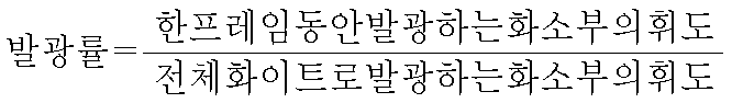
도 7을 참조하여 설명하면, 발광 제어부(220)는 화소부의 발광률에 따라 그 밝기를 제어하는 역할을 한다. 발광 제어부(220)는 데이터 합산부(221), 룩업 테이블(222) 및 휘도 제어 구동부(223)를 포함한다. Referring to FIG. 7, the light emission controller 220 controls the brightness according to the light emission rate of the pixel unit. The light emission controller 220 includes a
데이터 합산부(221)는 한 프레임 동안 발광하는 화소(50)들 각각에 입력된 비디오 데이터를 합한 값인 프레임 데이터에 대한 크기를 파악한다. 즉, 한 프레임 동안 발광하는 복수의 화소(1) 각각에 입력되는 비디오 데이터를 합하여 이를 프레임 데이터라 칭하고, 프레임 데이터의 크기가 크면 화소부(100)의 발광률이 높거나, 고계조의 화상을 표시하는 화소(1)가 많은 것을 의미한다. 즉, 프레임 데이터의 크기가 크면 화소부(100) 전체에 흐르는 전류의 양이 많다는 것을 의미하기 때문에 프레임 데이터의 크기가 소정의 값 이상이면 화소부(100)의 휘도를 제어하 여 전체 화소부(100)의 밝기를 감소시킨다. 그리고 화소부(100)의 밝기가 감소하는 경우에 발광하는 화소(1)는 높은 휘도를 갖게 되어 발광하지 않는 화소(1)와의 휘도 차이가 큰 상태 즉, 콘트라스트 비가 큰 상태를 유지하게 된다. 한편, 화소부(100)의 밝기가 감소하지 않는 경우에는 발광하는 화소(1)들의 발광 시간이 길게 유지됨으로써 그 휘도가 높아지게 되며 이에 따라 발광하는 화소(1)와 발광하지 않는 화소(1)의 명암비가 커지게 된다. 즉, 발광하는 화소(1)와 발광하지 않는 화소(1)의 명암비가 커짐으로써 화상이 더 선명하게 보일 수 있다. The
룩업 테이블(222)은 프레임 데이터의 상위 5비트 값에 대응하는 발광 제어신호의 발광 구간과 비발광 구간의 비율에 대한 정보를 저장하고 있다. 룩업 테이블(222)에 저장된 정보를 이용하여, 한 프레임 동안 발광하는 화소부(100)의 밝기를 파악할 수 있다. The lookup table 222 stores information on the ratio between the light emission period and the non-light emission period of the emission control signal corresponding to the upper 5 bit values of the frame data. The information stored in the lookup table 222 may be used to determine the brightness of the
휘도 제어 구동부(223)는 화소부(100)의 프레임 데이터의 크기가 소정의 크기 이상이 되면 휘도 제어 신호를 출력하고, 출력된 휘도 제어 신호에 대응하여 화소부(100)에 입력되는 발광 제어신호의 발광 구간과 비발광 구간의 비율을 조절한다. 이때, 화소부(100)의 휘도의 증가에 비례하여, 휘도 제어 비율을 계속해서 증가 시키면, 화소부(100)의 휘도가 아주 높아지는 경우, 지나친 휘도 제어로 인해 충분히 밝은 화면을 제공하지 못하며, 이는 단순히 전체적인 밝기를 떨어뜨리는 결과를 초래한다. 따라서, 휘도의 최대 제어 범위를 설정하여, 화소부(100) 전체의 밝기를 적당하게 조절하도록 한다. The
도 8은 본 발명에 따른 룩업 테이블의 실시 예를 나타낸 표이다. 8 is a table showing an embodiment of a lookup table according to the present invention.
도 8은 화소부(100)의 휘도에 따라 발광비를 최대값의 50%까지 제한한 룩업 테이블(222)을 나타낸 것이다. 도 8을 참조하여 설명하면, 8 illustrates a lookup table 222 in which the emission ratio is limited to 50% of the maximum value according to the luminance of the
화소부(100)의 발광하는 영역의 비율이 전체 화소부(100)의 36% 이하인 경우에는 화소부(100)의 휘도를 제한하지 않고, 화소부(100)의 발광하는 영역의 비율이 전체 화소부(100)의 36% 이상인 경우에는 화소부(100)의 휘도를 제한하여 화소부(100)가 최대 휘도로 발광하는 면적이 증가하면 이에 따라 휘도를 제한하는 비율도 증가하도록 한다. 이때 발광하는 영역의 비율은 수학식 1에 의해 결정되는 변수이다. When the ratio of the area where light is emitted in the
또한, 지나친 휘도의 제한을 방지하기 위해 최대 제한 비율을 50%로 제한하여, 화소(50)의 대부분이 최대 휘도로 발광한다 하더라도, 휘도 제한 비율이 50% 이상이 되지 않도록 한다. In addition, the maximum limiting ratio is limited to 50% to prevent excessive brightness limitation, so that even if most of the
도 9는 도 2의 발광 표시장치에 채용된 화소의 일례를 나타낸 도이다.FIG. 9 is a diagram illustrating an example of a pixel employed in the light emitting display device of FIG. 2.
도 9를 참조하여 설명하면, 화소(1)는 발광소자(OLED) 및 화소 회로를 포함 한다. 화소 회로는 제 1 트랜지스터(M1), 제 2 트랜지스터(M2), 제 3 트랜지스터(M3) 및 스토리지 커패시터(Cst)를 포함한다. 그리고 제 1 트랜지스터(M1), 제 2 트랜지스터(M2) 및 제 3 트랜지스터(M3)는 각각 게이트, 소스 및 드레인을 가지며 스토리지 커패시터(Cst)는 제 1 전극과 제 2 전극을 가진다. Referring to FIG. 9, the
제 1 트랜지스터(M1)는 소스가 제 1 전원(ELVdd)과 연결되고 드레인이 제 2 트랜지스터(M2)의 소스에 연결되며 게이트가 제 1 노드(A)와 연결된다. 제 1 노드(A)는 제 3 트랜지스터(M3)의 드레인과 연결된다. 제 1 트랜지스터(M1)는 데이터 신호에 대응되는 전류를 발광소자(OLED)에 공급하는 기능을 수행한다. The first transistor M1 has a source connected to the first power source ELVdd, a drain connected to the source of the second transistor M2, and a gate connected to the first node A. The first node A is connected to the drain of the third transistor M3. The first transistor M1 supplies a current corresponding to the data signal to the light emitting device OLED.
제 2 트랜지스터(M2)는 소스가 제 1 트랜지스터(M1)의 드레인과 연결되고, 드레인은 발광소자(OLED)의 애노드 전극에 연결되고, 게이트가 발광 제어선(En)에 연결되어 발광 제어신호에 응답한다. 따라서, 발광 제어신호에 따라 제1 트랜지스터(M1)에서 발광 소자(OLED)로 흐르는 전류의 흐름을 제어하여 발광 소자(OLED)의 발광을 제어한다. The second transistor M2 has a source connected to the drain of the first transistor M1, a drain connected to the anode electrode of the light emitting device OLED, and a gate connected to the emission control line En so as to be connected to the emission control signal. Answer. Accordingly, light emission of the light emitting device OLED is controlled by controlling the flow of current flowing from the first transistor M1 to the light emitting device OLED according to the light emission control signal.
제 3 트랜지스터(M3)는 소스가 데이터선(Dm)에 연결되고 드레인이 제 1 노드(A)와 연결되며 게이트는 주사선(Sn)과 연결된다. 그리고 게이트에 인가되는 주사 신호에 따라 데이터 신호를 제 1 노드(A)에 전달한다. The third transistor M3 has a source connected to the data line Dm, a drain connected to the first node A, and a gate connected to the scan line Sn. The data signal is transferred to the first node A according to the scan signal applied to the gate.
스토리지 커패시터(Cst)는 제 1 전극이 제 1 전원(ELVdd)과 연결되고 제 2 전극이 제 1 노드(A)에 연결된다. 그리고 데이터 신호에 따른 전하를 충전하며, 충전된 전하에 의해 한 프레임의 시간 동안 제 1 트랜지스터(M1)의 게이트에 신호를 인가하게 되어 제 1 트랜지스터(M1)의 동작을 한 프레임의 시간 동안 유지시킨 다. The storage capacitor Cst has a first electrode connected to the first power supply ELVdd and a second electrode connected to the first node A. FIG. In addition, the charge is charged according to the data signal, and the charged charge is applied to the gate of the first transistor M1 for one frame time, thereby maintaining the operation of the first transistor M1 for one frame time. All.
본 발명에 의한 발광 표시장치 및 그 구동 방법은 주변 광에 따라 휘도를 조절하고, 화소부의 발광량에 따라 그 밝기를 조절함으로써 시인성 향상 및 소비 전력 절감의 효과가 있다. The light emitting display device and the driving method thereof according to the present invention have an effect of improving visibility and reducing power consumption by adjusting the brightness according to the ambient light and the brightness according to the amount of light emitted from the pixel unit.
Claims (19)
Priority Applications (5)
| Application Number | Priority Date | Filing Date | Title |
|---|---|---|---|
| KR1020050035784A KR100707640B1 (en) | 2005-04-28 | 2005-04-28 | Light emitting display and driving method thereof |
| JP2005316860A JP4902172B2 (en) | 2005-04-28 | 2005-10-31 | Light emitting display device and driving method thereof |
| CNB2006100660295A CN100570688C (en) | 2005-04-28 | 2006-03-21 | Luminous display unit and driving method thereof |
| EP06251599.4A EP1717788B1 (en) | 2005-04-28 | 2006-03-24 | Light emitting display device and method of driving the same |
| US11/413,708 US7705811B2 (en) | 2005-04-28 | 2006-04-28 | Light emitting display device and method of driving the same |
Applications Claiming Priority (1)
| Application Number | Priority Date | Filing Date | Title |
|---|---|---|---|
| KR1020050035784A KR100707640B1 (en) | 2005-04-28 | 2005-04-28 | Light emitting display and driving method thereof |
Publications (2)
| Publication Number | Publication Date |
|---|---|
| KR20060113009A KR20060113009A (en) | 2006-11-02 |
| KR100707640B1 true KR100707640B1 (en) | 2007-04-12 |
Family
ID=36717065
Family Applications (1)
| Application Number | Title | Priority Date | Filing Date |
|---|---|---|---|
| KR1020050035784A KR100707640B1 (en) | 2005-04-28 | 2005-04-28 | Light emitting display and driving method thereof |
Country Status (5)
| Country | Link |
|---|---|
| US (1) | US7705811B2 (en) |
| EP (1) | EP1717788B1 (en) |
| JP (1) | JP4902172B2 (en) |
| KR (1) | KR100707640B1 (en) |
| CN (1) | CN100570688C (en) |
Cited By (1)
| Publication number | Priority date | Publication date | Assignee | Title |
|---|---|---|---|---|
| US9418589B2 (en) | 2012-07-25 | 2016-08-16 | Samsung Display Co., Ltd. | Display device for controlling light emission period based on the sum of gray values and driving method of the same |
Families Citing this family (118)
| Publication number | Priority date | Publication date | Assignee | Title |
|---|---|---|---|---|
| CA2443206A1 (en) | 2003-09-23 | 2005-03-23 | Ignis Innovation Inc. | Amoled display backplanes - pixel driver circuits, array architecture, and external compensation |
| CA2472671A1 (en) | 2004-06-29 | 2005-12-29 | Ignis Innovation Inc. | Voltage-programming scheme for current-driven amoled displays |
| CA2490858A1 (en) | 2004-12-07 | 2006-06-07 | Ignis Innovation Inc. | Driving method for compensated voltage-programming of amoled displays |
| US10013907B2 (en) | 2004-12-15 | 2018-07-03 | Ignis Innovation Inc. | Method and system for programming, calibrating and/or compensating, and driving an LED display |
| US9799246B2 (en) | 2011-05-20 | 2017-10-24 | Ignis Innovation Inc. | System and methods for extraction of threshold and mobility parameters in AMOLED displays |
| EP2688058A3 (en) | 2004-12-15 | 2014-12-10 | Ignis Innovation Inc. | Method and system for programming, calibrating and driving a light emitting device display |
| US9171500B2 (en) | 2011-05-20 | 2015-10-27 | Ignis Innovation Inc. | System and methods for extraction of parasitic parameters in AMOLED displays |
| US8576217B2 (en) | 2011-05-20 | 2013-11-05 | Ignis Innovation Inc. | System and methods for extraction of threshold and mobility parameters in AMOLED displays |
| US9280933B2 (en) | 2004-12-15 | 2016-03-08 | Ignis Innovation Inc. | System and methods for extraction of threshold and mobility parameters in AMOLED displays |
| US10012678B2 (en) | 2004-12-15 | 2018-07-03 | Ignis Innovation Inc. | Method and system for programming, calibrating and/or compensating, and driving an LED display |
| US9275579B2 (en) | 2004-12-15 | 2016-03-01 | Ignis Innovation Inc. | System and methods for extraction of threshold and mobility parameters in AMOLED displays |
| US20140111567A1 (en) | 2005-04-12 | 2014-04-24 | Ignis Innovation Inc. | System and method for compensation of non-uniformities in light emitting device displays |
| CA2496642A1 (en) | 2005-02-10 | 2006-08-10 | Ignis Innovation Inc. | Fast settling time driving method for organic light-emitting diode (oled) displays based on current programming |
| JP5355080B2 (en) | 2005-06-08 | 2013-11-27 | イグニス・イノベイション・インコーポレーテッド | Method and system for driving a light emitting device display |
| CA2518276A1 (en) | 2005-09-13 | 2007-03-13 | Ignis Innovation Inc. | Compensation technique for luminance degradation in electro-luminance devices |
| US9489891B2 (en) | 2006-01-09 | 2016-11-08 | Ignis Innovation Inc. | Method and system for driving an active matrix display circuit |
| US9269322B2 (en) | 2006-01-09 | 2016-02-23 | Ignis Innovation Inc. | Method and system for driving an active matrix display circuit |
| KR20090006057A (en) | 2006-01-09 | 2009-01-14 | 이그니스 이노베이션 인크. | Method and system for driving an active matrix display circuit |
| WO2007118332A1 (en) | 2006-04-19 | 2007-10-25 | Ignis Innovation Inc. | Stable driving scheme for active matrix displays |
| CA2556961A1 (en) | 2006-08-15 | 2008-02-15 | Ignis Innovation Inc. | Oled compensation technique based on oled capacitance |
| KR100830297B1 (en) * | 2006-09-26 | 2008-05-19 | 삼성에스디아이 주식회사 | Light emitting display device and driving method for same |
| KR100836424B1 (en) | 2007-02-05 | 2008-06-09 | 삼성에스디아이 주식회사 | Organic light emitting display device and driving method thereof |
| KR100836433B1 (en) | 2007-02-05 | 2008-06-09 | 삼성에스디아이 주식회사 | Organic light emitting display device and driving method thereof |
| KR100836425B1 (en) | 2007-02-05 | 2008-06-09 | 삼성에스디아이 주식회사 | Organic light emitting display device and driving method thereof |
| KR100836438B1 (en) | 2007-02-05 | 2008-06-09 | 삼성에스디아이 주식회사 | Organic light emitting display device and driving method thereof |
| KR100836432B1 (en) | 2007-02-05 | 2008-06-09 | 삼성에스디아이 주식회사 | Organic light emitting display device and driving method thereof |
| KR100844774B1 (en) * | 2007-02-23 | 2008-07-07 | 삼성에스디아이 주식회사 | Driving method of organic light emitting display device |
| JP2008209886A (en) * | 2007-02-23 | 2008-09-11 | Samsung Sdi Co Ltd | Organic electroluminescence display and drive method therefor |
| KR100840102B1 (en) | 2007-02-23 | 2008-06-19 | 삼성에스디아이 주식회사 | Organic light emitting display and drinvig method thereof |
| KR100844781B1 (en) | 2007-02-23 | 2008-07-07 | 삼성에스디아이 주식회사 | Organic light emitting diodes display device and driving method thereof |
| KR100844777B1 (en) * | 2007-02-23 | 2008-07-07 | 삼성에스디아이 주식회사 | Organic light emitting diodes display device |
| KR100840097B1 (en) * | 2007-02-23 | 2008-06-19 | 삼성에스디아이 주식회사 | Organic light emitting diodes display device |
| KR100844776B1 (en) * | 2007-02-23 | 2008-07-07 | 삼성에스디아이 주식회사 | Organic light emitting display device and dirving method thereof |
| KR100844780B1 (en) * | 2007-02-23 | 2008-07-07 | 삼성에스디아이 주식회사 | Organic light emitting diodes display device and driving method thereof |
| KR100844775B1 (en) | 2007-02-23 | 2008-07-07 | 삼성에스디아이 주식회사 | Organic light emitting display device |
| KR100857688B1 (en) * | 2007-03-08 | 2008-09-08 | 삼성에스디아이 주식회사 | Organic light emitting display and making method the same |
| KR100858614B1 (en) * | 2007-03-08 | 2008-09-17 | 삼성에스디아이 주식회사 | Organic light emitting display and driving method the same |
| KR20080086747A (en) * | 2007-03-23 | 2008-09-26 | 삼성에스디아이 주식회사 | Organic light emitting display and driving method thereof |
| KR100873707B1 (en) * | 2007-07-27 | 2008-12-12 | 삼성모바일디스플레이주식회사 | Organic light emitting display and driving method thereof |
| KR100893480B1 (en) * | 2007-08-02 | 2009-04-17 | 삼성모바일디스플레이주식회사 | Organic light emitting display and driving method teherof |
| JP4627773B2 (en) * | 2007-10-16 | 2011-02-09 | Okiセミコンダクタ株式会社 | Drive circuit device |
| KR100876276B1 (en) * | 2007-10-29 | 2008-12-26 | 삼성모바일디스플레이주식회사 | Organic light emitting display |
| KR20090084444A (en) | 2008-02-01 | 2009-08-05 | 삼성모바일디스플레이주식회사 | Organic light emitting display and driving method thereof |
| KR100958028B1 (en) * | 2008-02-13 | 2010-05-17 | 삼성모바일디스플레이주식회사 | Photo sensor and flat panel display usinig the same |
| WO2009127065A1 (en) | 2008-04-18 | 2009-10-22 | Ignis Innovation Inc. | System and driving method for light emitting device display |
| KR100963058B1 (en) | 2008-05-09 | 2010-06-14 | 삼성모바일디스플레이주식회사 | Organic light emitting display and driving method thereof |
| KR101352189B1 (en) * | 2008-07-08 | 2014-01-16 | 엘지디스플레이 주식회사 | Gamma Reference Voltage Generation Circuit And Flat Panel Display Using It |
| CA2637343A1 (en) | 2008-07-29 | 2010-01-29 | Ignis Innovation Inc. | Improving the display source driver |
| US9370075B2 (en) | 2008-12-09 | 2016-06-14 | Ignis Innovation Inc. | System and method for fast compensation programming of pixels in a display |
| US9384698B2 (en) | 2009-11-30 | 2016-07-05 | Ignis Innovation Inc. | System and methods for aging compensation in AMOLED displays |
| CA2669367A1 (en) | 2009-06-16 | 2010-12-16 | Ignis Innovation Inc | Compensation technique for color shift in displays |
| CA2688870A1 (en) | 2009-11-30 | 2011-05-30 | Ignis Innovation Inc. | Methode and techniques for improving display uniformity |
| US9311859B2 (en) | 2009-11-30 | 2016-04-12 | Ignis Innovation Inc. | Resetting cycle for aging compensation in AMOLED displays |
| US10319307B2 (en) | 2009-06-16 | 2019-06-11 | Ignis Innovation Inc. | Display system with compensation techniques and/or shared level resources |
| JP5493733B2 (en) * | 2009-11-09 | 2014-05-14 | ソニー株式会社 | Display device and electronic device |
| US8283967B2 (en) | 2009-11-12 | 2012-10-09 | Ignis Innovation Inc. | Stable current source for system integration to display substrate |
| KR101042956B1 (en) * | 2009-11-18 | 2011-06-20 | 삼성모바일디스플레이주식회사 | Pixel circuit and organic light emitting display using thereof |
| US10996258B2 (en) | 2009-11-30 | 2021-05-04 | Ignis Innovation Inc. | Defect detection and correction of pixel circuits for AMOLED displays |
| US8803417B2 (en) | 2009-12-01 | 2014-08-12 | Ignis Innovation Inc. | High resolution pixel architecture |
| CA2687631A1 (en) * | 2009-12-06 | 2011-06-06 | Ignis Innovation Inc | Low power driving scheme for display applications |
| US20140313111A1 (en) | 2010-02-04 | 2014-10-23 | Ignis Innovation Inc. | System and methods for extracting correlation curves for an organic light emitting device |
| US10176736B2 (en) | 2010-02-04 | 2019-01-08 | Ignis Innovation Inc. | System and methods for extracting correlation curves for an organic light emitting device |
| US10163401B2 (en) | 2010-02-04 | 2018-12-25 | Ignis Innovation Inc. | System and methods for extracting correlation curves for an organic light emitting device |
| US10089921B2 (en) | 2010-02-04 | 2018-10-02 | Ignis Innovation Inc. | System and methods for extracting correlation curves for an organic light emitting device |
| US9881532B2 (en) | 2010-02-04 | 2018-01-30 | Ignis Innovation Inc. | System and method for extracting correlation curves for an organic light emitting device |
| CA2692097A1 (en) | 2010-02-04 | 2011-08-04 | Ignis Innovation Inc. | Extracting correlation curves for light emitting device |
| CA2696778A1 (en) | 2010-03-17 | 2011-09-17 | Ignis Innovation Inc. | Lifetime, uniformity, parameter extraction methods |
| US8907991B2 (en) | 2010-12-02 | 2014-12-09 | Ignis Innovation Inc. | System and methods for thermal compensation in AMOLED displays |
| TW201248604A (en) * | 2011-05-16 | 2012-12-01 | Novatek Microelectronics Corp | Display apparatus and image compensating method thereof |
| US9886899B2 (en) | 2011-05-17 | 2018-02-06 | Ignis Innovation Inc. | Pixel Circuits for AMOLED displays |
| US20140368491A1 (en) | 2013-03-08 | 2014-12-18 | Ignis Innovation Inc. | Pixel circuits for amoled displays |
| US9351368B2 (en) | 2013-03-08 | 2016-05-24 | Ignis Innovation Inc. | Pixel circuits for AMOLED displays |
| US9530349B2 (en) | 2011-05-20 | 2016-12-27 | Ignis Innovations Inc. | Charged-based compensation and parameter extraction in AMOLED displays |
| US9466240B2 (en) | 2011-05-26 | 2016-10-11 | Ignis Innovation Inc. | Adaptive feedback system for compensating for aging pixel areas with enhanced estimation speed |
| CN102800301A (en) * | 2011-05-27 | 2012-11-28 | 联咏科技股份有限公司 | Display device and image compensation method thereof |
| EP3293726B1 (en) | 2011-05-27 | 2019-08-14 | Ignis Innovation Inc. | Systems and methods for aging compensation in amoled displays |
| EP2945147B1 (en) | 2011-05-28 | 2018-08-01 | Ignis Innovation Inc. | Method for fast compensation programming of pixels in a display |
| CN104115555B (en) * | 2011-10-12 | 2017-02-15 | Dialog半导体有限公司 | Programmable solid state light bulb assemblies |
| US10089924B2 (en) | 2011-11-29 | 2018-10-02 | Ignis Innovation Inc. | Structural and low-frequency non-uniformity compensation |
| US9324268B2 (en) | 2013-03-15 | 2016-04-26 | Ignis Innovation Inc. | Amoled displays with multiple readout circuits |
| US8937632B2 (en) | 2012-02-03 | 2015-01-20 | Ignis Innovation Inc. | Driving system for active-matrix displays |
| US9747834B2 (en) | 2012-05-11 | 2017-08-29 | Ignis Innovation Inc. | Pixel circuits including feedback capacitors and reset capacitors, and display systems therefore |
| US8922544B2 (en) | 2012-05-23 | 2014-12-30 | Ignis Innovation Inc. | Display systems with compensation for line propagation delay |
| US9336717B2 (en) | 2012-12-11 | 2016-05-10 | Ignis Innovation Inc. | Pixel circuits for AMOLED displays |
| US9786223B2 (en) | 2012-12-11 | 2017-10-10 | Ignis Innovation Inc. | Pixel circuits for AMOLED displays |
| US9830857B2 (en) | 2013-01-14 | 2017-11-28 | Ignis Innovation Inc. | Cleaning common unwanted signals from pixel measurements in emissive displays |
| US9171504B2 (en) | 2013-01-14 | 2015-10-27 | Ignis Innovation Inc. | Driving scheme for emissive displays providing compensation for driving transistor variations |
| CA2894717A1 (en) | 2015-06-19 | 2016-12-19 | Ignis Innovation Inc. | Optoelectronic device characterization in array with shared sense line |
| US9721505B2 (en) | 2013-03-08 | 2017-08-01 | Ignis Innovation Inc. | Pixel circuits for AMOLED displays |
| EP3043338A1 (en) | 2013-03-14 | 2016-07-13 | Ignis Innovation Inc. | Re-interpolation with edge detection for extracting an aging pattern for amoled displays |
| CN105144361B (en) | 2013-04-22 | 2019-09-27 | 伊格尼斯创新公司 | Detection system for OLED display panel |
| KR102147506B1 (en) * | 2013-07-15 | 2020-08-25 | 삼성디스플레이 주식회사 | Gamma voltage supply device and display device using thereof |
| DE112014003719T5 (en) | 2013-08-12 | 2016-05-19 | Ignis Innovation Inc. | compensation accuracy |
| US9741282B2 (en) | 2013-12-06 | 2017-08-22 | Ignis Innovation Inc. | OLED display system and method |
| US9761170B2 (en) | 2013-12-06 | 2017-09-12 | Ignis Innovation Inc. | Correction for localized phenomena in an image array |
| US9502653B2 (en) | 2013-12-25 | 2016-11-22 | Ignis Innovation Inc. | Electrode contacts |
| DE102015206281A1 (en) | 2014-04-08 | 2015-10-08 | Ignis Innovation Inc. | Display system with shared level resources for portable devices |
| KR102218642B1 (en) * | 2014-11-27 | 2021-02-23 | 삼성디스플레이 주식회사 | Display device and method of driving a display device |
| CA2873476A1 (en) | 2014-12-08 | 2016-06-08 | Ignis Innovation Inc. | Smart-pixel display architecture |
| CA2879462A1 (en) | 2015-01-23 | 2016-07-23 | Ignis Innovation Inc. | Compensation for color variation in emissive devices |
| CA2886862A1 (en) | 2015-04-01 | 2016-10-01 | Ignis Innovation Inc. | Adjusting display brightness for avoiding overheating and/or accelerated aging |
| CA2889870A1 (en) | 2015-05-04 | 2016-11-04 | Ignis Innovation Inc. | Optical feedback system |
| CA2892714A1 (en) | 2015-05-27 | 2016-11-27 | Ignis Innovation Inc | Memory bandwidth reduction in compensation system |
| CA2898282A1 (en) | 2015-07-24 | 2017-01-24 | Ignis Innovation Inc. | Hybrid calibration of current sources for current biased voltage progra mmed (cbvp) displays |
| US10657895B2 (en) | 2015-07-24 | 2020-05-19 | Ignis Innovation Inc. | Pixels and reference circuits and timing techniques |
| US10373554B2 (en) | 2015-07-24 | 2019-08-06 | Ignis Innovation Inc. | Pixels and reference circuits and timing techniques |
| CA2900170A1 (en) | 2015-08-07 | 2017-02-07 | Gholamreza Chaji | Calibration of pixel based on improved reference values |
| CA2908285A1 (en) | 2015-10-14 | 2017-04-14 | Ignis Innovation Inc. | Driver with multiple color pixel structure |
| KR20170045452A (en) * | 2015-10-16 | 2017-04-27 | 삼성디스플레이 주식회사 | Backlight unit, method for driving thereof, and display device including the same |
| US10297191B2 (en) | 2016-01-29 | 2019-05-21 | Samsung Display Co., Ltd. | Dynamic net power control for OLED and local dimming LCD displays |
| CN109147664B (en) * | 2017-06-15 | 2022-07-12 | 上海和辉光电股份有限公司 | AMOLED display screen |
| US10861380B2 (en) * | 2018-05-14 | 2020-12-08 | Facebook Technologies, Llc | Display systems with hybrid emitter circuits |
| TWI696161B (en) * | 2018-12-28 | 2020-06-11 | 奇景光電股份有限公司 | Accumulated luminance compensation system and oled display |
| JP2020144256A (en) * | 2019-03-07 | 2020-09-10 | シナプティクス インコーポレイテッド | Display driver and method for driving self-luminous display panel |
| CN111724731A (en) * | 2019-03-20 | 2020-09-29 | 三星显示有限公司 | Luminance control unit and display device including the same |
| JP2022098627A (en) | 2020-12-22 | 2022-07-04 | セイコーエプソン株式会社 | Electro-optical device and electronic apparatus |
| JP2022099497A (en) * | 2020-12-23 | 2022-07-05 | セイコーエプソン株式会社 | Electro-optical device and electronic apparatus |
| TWI777386B (en) * | 2021-01-25 | 2022-09-11 | 大陸商北京歐錸德微電子技術有限公司 | Display driver chip and display and information processing device using the same |
Citations (2)
| Publication number | Priority date | Publication date | Assignee | Title |
|---|---|---|---|---|
| KR20000033177A (en) * | 1998-11-20 | 2000-06-15 | 구자홍 | Method for operating self emitting device |
| JP2000221944A (en) * | 1999-02-01 | 2000-08-11 | Denso Corp | Driving method of el display device, and el display device |
Family Cites Families (32)
| Publication number | Priority date | Publication date | Assignee | Title |
|---|---|---|---|---|
| JPH0588655A (en) | 1991-09-27 | 1993-04-09 | Toshiba Corp | Image brightness controller |
| DE69740083D1 (en) * | 1997-06-05 | 2011-02-03 | Thomson Multimedia Sa | Liquid crystal display for direct viewing with automatic color adjustment |
| JPH11175027A (en) * | 1997-12-08 | 1999-07-02 | Hitachi Ltd | Liquid crystal driving circuit and liquid crystal display device |
| JPH11194739A (en) | 1997-12-27 | 1999-07-21 | Canon Inc | Image display device and image forming device |
| US6611249B1 (en) * | 1998-07-22 | 2003-08-26 | Silicon Graphics, Inc. | System and method for providing a wide aspect ratio flat panel display monitor independent white-balance adjustment and gamma correction capabilities |
| JP2000293133A (en) * | 1999-04-05 | 2000-10-20 | Matsushita Electric Ind Co Ltd | Display device |
| JP3763397B2 (en) * | 2000-03-24 | 2006-04-05 | シャープ株式会社 | Image processing apparatus, image display apparatus, personal computer, and image processing method |
| US6995753B2 (en) * | 2000-06-06 | 2006-02-07 | Semiconductor Energy Laboratory Co., Ltd. | Display device and method of manufacturing the same |
| TW554625B (en) * | 2000-12-08 | 2003-09-21 | Silicon Graphics Inc | Compact flat panel color calibration system |
| JP2002366112A (en) * | 2001-06-07 | 2002-12-20 | Hitachi Ltd | Liquid crystal driving device and liquid crystal display device |
| KR100714513B1 (en) * | 2001-09-07 | 2007-05-07 | 마츠시타 덴끼 산교 가부시키가이샤 | El display, el display driving circuit and image display |
| EP1450341A4 (en) * | 2001-09-25 | 2009-04-01 | Panasonic Corp | El display panel and el display apparatus comprising it |
| JP4293747B2 (en) | 2001-12-26 | 2009-07-08 | ソニー株式会社 | Organic EL display device and control method thereof |
| JP2003228330A (en) * | 2002-02-01 | 2003-08-15 | Sanyo Electric Co Ltd | Display device |
| JP3724430B2 (en) * | 2002-02-04 | 2005-12-07 | ソニー株式会社 | Organic EL display device and control method thereof |
| JP2003308046A (en) * | 2002-02-18 | 2003-10-31 | Sanyo Electric Co Ltd | Display device |
| US7255991B2 (en) * | 2002-03-22 | 2007-08-14 | Emory University | Template-drive processes for synthesizing polymers and components related to such processes |
| KR101017797B1 (en) * | 2002-04-26 | 2011-02-28 | 도시바 모바일 디스플레이 가부시키가이샤 | El display device and driving method thereof |
| CN100401357C (en) | 2002-09-04 | 2008-07-09 | 皇家飞利浦电子股份有限公司 | Electroluminescent display devices |
| JP2004138831A (en) * | 2002-10-17 | 2004-05-13 | Kodak Kk | Organic electroluminescence display device |
| JP2004151187A (en) * | 2002-10-29 | 2004-05-27 | Matsushita Electric Ind Co Ltd | Led display device with automatic gamma correction curve changing function and automatic gamma correction curve changing program |
| ES2380661T3 (en) | 2002-12-04 | 2012-05-17 | Koninklijke Philips Electronics N.V. | An organic led display device and method to excite it |
| KR100555303B1 (en) * | 2002-12-11 | 2006-03-03 | 엘지.필립스 엘시디 주식회사 | Apparatus and method of generating gamma voltage |
| US20060055828A1 (en) * | 2002-12-13 | 2006-03-16 | Koninklijke Philips Electronics N.V. | Automatic gamma correction for a matrix display |
| KR100565591B1 (en) | 2003-01-17 | 2006-03-30 | 엘지전자 주식회사 | method for driving of self-light emitting device |
| JP2004361816A (en) * | 2003-06-06 | 2004-12-24 | Toshiba Matsushita Display Technology Co Ltd | El display device |
| JP2005004118A (en) * | 2003-06-16 | 2005-01-06 | Hitachi Ltd | Display device |
| CN1816839A (en) * | 2003-07-09 | 2006-08-09 | 皇家飞利浦电子股份有限公司 | Electroluminescent display device with duty cycle control |
| EP1505566B1 (en) | 2003-07-30 | 2016-03-09 | LG Display Co., Ltd. | Gamma voltage generating apparatus |
| JP2005062485A (en) * | 2003-08-12 | 2005-03-10 | Toshiba Matsushita Display Technology Co Ltd | Organic el display device and its driving method |
| JP2005055726A (en) * | 2003-08-06 | 2005-03-03 | Toshiba Matsushita Display Technology Co Ltd | El display device |
| KR101121617B1 (en) * | 2004-04-29 | 2012-02-28 | 엘지디스플레이 주식회사 | Electro-Luminescence Display Apparatus |
-
2005
- 2005-04-28 KR KR1020050035784A patent/KR100707640B1/en active IP Right Grant
- 2005-10-31 JP JP2005316860A patent/JP4902172B2/en active Active
-
2006
- 2006-03-21 CN CNB2006100660295A patent/CN100570688C/en active Active
- 2006-03-24 EP EP06251599.4A patent/EP1717788B1/en active Active
- 2006-04-28 US US11/413,708 patent/US7705811B2/en active Active
Patent Citations (2)
| Publication number | Priority date | Publication date | Assignee | Title |
|---|---|---|---|---|
| KR20000033177A (en) * | 1998-11-20 | 2000-06-15 | 구자홍 | Method for operating self emitting device |
| JP2000221944A (en) * | 1999-02-01 | 2000-08-11 | Denso Corp | Driving method of el display device, and el display device |
Non-Patent Citations (2)
| Title |
|---|
| 1020000033177 |
| 12221944 |
Cited By (1)
| Publication number | Priority date | Publication date | Assignee | Title |
|---|---|---|---|---|
| US9418589B2 (en) | 2012-07-25 | 2016-08-16 | Samsung Display Co., Ltd. | Display device for controlling light emission period based on the sum of gray values and driving method of the same |
Also Published As
| Publication number | Publication date |
|---|---|
| JP4902172B2 (en) | 2012-03-21 |
| CN100570688C (en) | 2009-12-16 |
| EP1717788B1 (en) | 2017-06-21 |
| US20060244697A1 (en) | 2006-11-02 |
| CN1855202A (en) | 2006-11-01 |
| EP1717788A2 (en) | 2006-11-02 |
| EP1717788A3 (en) | 2009-12-02 |
| JP2006309127A (en) | 2006-11-09 |
| KR20060113009A (en) | 2006-11-02 |
| US7705811B2 (en) | 2010-04-27 |
Similar Documents
| Publication | Publication Date | Title |
|---|---|---|
| KR100707640B1 (en) | Light emitting display and driving method thereof | |
| US8154478B2 (en) | Organic electro luminescence display and driving method thereof | |
| KR100748319B1 (en) | Light emitting display device and driving method for same | |
| KR100830297B1 (en) | Light emitting display device and driving method for same | |
| US8022902B2 (en) | Organic light emitting display device and driving method thereof | |
| JP5032807B2 (en) | Flat panel display and control method of flat panel display | |
| KR100836432B1 (en) | Organic light emitting display device and driving method thereof | |
| KR100844775B1 (en) | Organic light emitting display device | |
| KR100836438B1 (en) | Organic light emitting display device and driving method thereof | |
| EP1962268A1 (en) | Organic elecroluminescence display (OLED) and driving methods thereof | |
| KR100793542B1 (en) | Organic electro luminescence display and driving method thereof | |
| KR100836424B1 (en) | Organic light emitting display device and driving method thereof | |
| KR101510690B1 (en) | Driving Circuit For Automatic Adjustment Of Grey Level Voltage Using Transfer Function And Display Device Including The Same | |
| KR100748320B1 (en) | Organic light emitting display device and driving method for the same | |
| US20070262927A1 (en) | Electron emission display device and driving method thereof | |
| KR100844776B1 (en) | Organic light emitting display device and dirving method thereof | |
| KR100840097B1 (en) | Organic light emitting diodes display device | |
| KR100844777B1 (en) | Organic light emitting diodes display device | |
| KR100646987B1 (en) | Organic light emitting display and the control method of the same | |
| KR100658268B1 (en) | Organic light emitting display device and control method of the same | |
| KR100893480B1 (en) | Organic light emitting display and driving method teherof |
Legal Events
| Date | Code | Title | Description |
|---|---|---|---|
| A201 | Request for examination | ||
| E902 | Notification of reason for refusal | ||
| E701 | Decision to grant or registration of patent right | ||
| GRNT | Written decision to grant | ||
| FPAY | Annual fee payment |
Payment date: 20130329 Year of fee payment: 7 |
|
| FPAY | Annual fee payment |
Payment date: 20140401 Year of fee payment: 8 |
|
| FPAY | Annual fee payment |
Payment date: 20160329 Year of fee payment: 10 |
|
| FPAY | Annual fee payment |
Payment date: 20180403 Year of fee payment: 12 |
|
| FPAY | Annual fee payment |
Payment date: 20190401 Year of fee payment: 13 |