JP4703815B2 - MOS type sensor driving method and imaging method - Google Patents
MOS type sensor driving method and imaging method Download PDFInfo
- Publication number
- JP4703815B2 JP4703815B2 JP2000156111A JP2000156111A JP4703815B2 JP 4703815 B2 JP4703815 B2 JP 4703815B2 JP 2000156111 A JP2000156111 A JP 2000156111A JP 2000156111 A JP2000156111 A JP 2000156111A JP 4703815 B2 JP4703815 B2 JP 4703815B2
- Authority
- JP
- Japan
- Prior art keywords
- signal
- pixels
- reset
- imaging unit
- time
- Prior art date
- Legal status (The legal status is an assumption and is not a legal conclusion. Google has not performed a legal analysis and makes no representation as to the accuracy of the status listed.)
- Expired - Fee Related
Links
- 238000003384 imaging method Methods 0.000 title claims description 187
- 238000000034 method Methods 0.000 title claims description 47
- 238000009825 accumulation Methods 0.000 claims description 124
- 238000006243 chemical reaction Methods 0.000 claims description 88
- 230000003321 amplification Effects 0.000 claims description 56
- 238000003199 nucleic acid amplification method Methods 0.000 claims description 56
- 229920006395 saturated elastomer Polymers 0.000 claims description 37
- 238000001444 catalytic combustion detection Methods 0.000 description 35
- 238000010586 diagram Methods 0.000 description 33
- 239000012535 impurity Substances 0.000 description 25
- 238000012546 transfer Methods 0.000 description 22
- 239000003990 capacitor Substances 0.000 description 20
- 239000011229 interlayer Substances 0.000 description 13
- 229910021417 amorphous silicon Inorganic materials 0.000 description 12
- 230000008859 change Effects 0.000 description 12
- 239000000758 substrate Substances 0.000 description 12
- 239000010410 layer Substances 0.000 description 11
- 239000010936 titanium Substances 0.000 description 9
- OAICVXFJPJFONN-UHFFFAOYSA-N Phosphorus Chemical compound [P] OAICVXFJPJFONN-UHFFFAOYSA-N 0.000 description 8
- 229910021419 crystalline silicon Inorganic materials 0.000 description 8
- 239000000463 material Substances 0.000 description 8
- 229910052698 phosphorus Inorganic materials 0.000 description 8
- 239000011574 phosphorus Substances 0.000 description 8
- 238000012545 processing Methods 0.000 description 8
- UFHFLCQGNIYNRP-UHFFFAOYSA-N Hydrogen Chemical compound [H][H] UFHFLCQGNIYNRP-UHFFFAOYSA-N 0.000 description 7
- 229910052581 Si3N4 Inorganic materials 0.000 description 7
- 239000001257 hydrogen Substances 0.000 description 7
- 229910052739 hydrogen Inorganic materials 0.000 description 7
- HQVNEWCFYHHQES-UHFFFAOYSA-N silicon nitride Chemical compound N12[Si]34N5[Si]62N3[Si]51N64 HQVNEWCFYHHQES-UHFFFAOYSA-N 0.000 description 7
- 230000004913 activation Effects 0.000 description 6
- 238000010438 heat treatment Methods 0.000 description 6
- 238000004519 manufacturing process Methods 0.000 description 6
- 239000004065 semiconductor Substances 0.000 description 6
- RTAQQCXQSZGOHL-UHFFFAOYSA-N Titanium Chemical compound [Ti] RTAQQCXQSZGOHL-UHFFFAOYSA-N 0.000 description 5
- 229910052782 aluminium Inorganic materials 0.000 description 5
- XAGFODPZIPBFFR-UHFFFAOYSA-N aluminium Chemical compound [Al] XAGFODPZIPBFFR-UHFFFAOYSA-N 0.000 description 5
- 238000002425 crystallisation Methods 0.000 description 5
- 230000001066 destructive effect Effects 0.000 description 5
- 239000011521 glass Substances 0.000 description 5
- 238000005984 hydrogenation reaction Methods 0.000 description 5
- 230000010355 oscillation Effects 0.000 description 5
- 230000001681 protective effect Effects 0.000 description 5
- 238000004544 sputter deposition Methods 0.000 description 5
- 229910052719 titanium Inorganic materials 0.000 description 5
- ZOXJGFHDIHLPTG-UHFFFAOYSA-N Boron Chemical compound [B] ZOXJGFHDIHLPTG-UHFFFAOYSA-N 0.000 description 4
- XYFCBTPGUUZFHI-UHFFFAOYSA-N Phosphine Chemical compound P XYFCBTPGUUZFHI-UHFFFAOYSA-N 0.000 description 4
- XUIMIQQOPSSXEZ-UHFFFAOYSA-N Silicon Chemical compound [Si] XUIMIQQOPSSXEZ-UHFFFAOYSA-N 0.000 description 4
- NIXOWILDQLNWCW-UHFFFAOYSA-N acrylic acid group Chemical group C(C=C)(=O)O NIXOWILDQLNWCW-UHFFFAOYSA-N 0.000 description 4
- 238000000137 annealing Methods 0.000 description 4
- 229910052796 boron Inorganic materials 0.000 description 4
- 238000007599 discharging Methods 0.000 description 4
- 238000002347 injection Methods 0.000 description 4
- 239000007924 injection Substances 0.000 description 4
- 238000002161 passivation Methods 0.000 description 4
- 229920001721 polyimide Polymers 0.000 description 4
- 229910052710 silicon Inorganic materials 0.000 description 4
- 239000010703 silicon Substances 0.000 description 4
- 239000002356 single layer Substances 0.000 description 4
- 238000003860 storage Methods 0.000 description 4
- 229910052721 tungsten Inorganic materials 0.000 description 4
- 239000010937 tungsten Substances 0.000 description 4
- 239000004642 Polyimide Substances 0.000 description 3
- VYPSYNLAJGMNEJ-UHFFFAOYSA-N Silicium dioxide Chemical compound O=[Si]=O VYPSYNLAJGMNEJ-UHFFFAOYSA-N 0.000 description 3
- 239000012298 atmosphere Substances 0.000 description 3
- QVGXLLKOCUKJST-UHFFFAOYSA-N atomic oxygen Chemical compound [O] QVGXLLKOCUKJST-UHFFFAOYSA-N 0.000 description 3
- 230000015572 biosynthetic process Effects 0.000 description 3
- 230000007423 decrease Effects 0.000 description 3
- 239000007789 gas Substances 0.000 description 3
- 230000001678 irradiating effect Effects 0.000 description 3
- 238000005224 laser annealing Methods 0.000 description 3
- 239000001301 oxygen Substances 0.000 description 3
- 229910052760 oxygen Inorganic materials 0.000 description 3
- 229920005989 resin Polymers 0.000 description 3
- 239000011347 resin Substances 0.000 description 3
- 229910052814 silicon oxide Inorganic materials 0.000 description 3
- 230000007704 transition Effects 0.000 description 3
- WFKWXMTUELFFGS-UHFFFAOYSA-N tungsten Chemical compound [W] WFKWXMTUELFFGS-UHFFFAOYSA-N 0.000 description 3
- XKRFYHLGVUSROY-UHFFFAOYSA-N Argon Chemical compound [Ar] XKRFYHLGVUSROY-UHFFFAOYSA-N 0.000 description 2
- IJGRMHOSHXDMSA-UHFFFAOYSA-N Atomic nitrogen Chemical compound N#N IJGRMHOSHXDMSA-UHFFFAOYSA-N 0.000 description 2
- 239000004952 Polyamide Substances 0.000 description 2
- 230000008901 benefit Effects 0.000 description 2
- UMIVXZPTRXBADB-UHFFFAOYSA-N benzocyclobutene Chemical compound C1=CC=C2CCC2=C1 UMIVXZPTRXBADB-UHFFFAOYSA-N 0.000 description 2
- 238000005513 bias potential Methods 0.000 description 2
- 239000011651 chromium Substances 0.000 description 2
- 238000011161 development Methods 0.000 description 2
- 230000000694 effects Effects 0.000 description 2
- 238000005286 illumination Methods 0.000 description 2
- 239000011159 matrix material Substances 0.000 description 2
- 229910021421 monocrystalline silicon Inorganic materials 0.000 description 2
- 230000002093 peripheral effect Effects 0.000 description 2
- 229910000073 phosphorus hydride Inorganic materials 0.000 description 2
- 229920002647 polyamide Polymers 0.000 description 2
- 229910021420 polycrystalline silicon Inorganic materials 0.000 description 2
- 230000000750 progressive effect Effects 0.000 description 2
- 230000009467 reduction Effects 0.000 description 2
- 230000002441 reversible effect Effects 0.000 description 2
- 238000000926 separation method Methods 0.000 description 2
- GGCZERPQGJTIQP-UHFFFAOYSA-N sodium;9,10-dioxoanthracene-2-sulfonic acid Chemical compound [Na+].C1=CC=C2C(=O)C3=CC(S(=O)(=O)O)=CC=C3C(=O)C2=C1 GGCZERPQGJTIQP-UHFFFAOYSA-N 0.000 description 2
- 229910052715 tantalum Inorganic materials 0.000 description 2
- GUVRBAGPIYLISA-UHFFFAOYSA-N tantalum atom Chemical compound [Ta] GUVRBAGPIYLISA-UHFFFAOYSA-N 0.000 description 2
- 229910000838 Al alloy Inorganic materials 0.000 description 1
- OKTJSMMVPCPJKN-UHFFFAOYSA-N Carbon Chemical compound [C] OKTJSMMVPCPJKN-UHFFFAOYSA-N 0.000 description 1
- VYZAMTAEIAYCRO-UHFFFAOYSA-N Chromium Chemical compound [Cr] VYZAMTAEIAYCRO-UHFFFAOYSA-N 0.000 description 1
- RYGMFSIKBFXOCR-UHFFFAOYSA-N Copper Chemical compound [Cu] RYGMFSIKBFXOCR-UHFFFAOYSA-N 0.000 description 1
- 241001649012 Cypselea humifusa Species 0.000 description 1
- ZOKXTWBITQBERF-UHFFFAOYSA-N Molybdenum Chemical compound [Mo] ZOKXTWBITQBERF-UHFFFAOYSA-N 0.000 description 1
- 229910001362 Ta alloys Inorganic materials 0.000 description 1
- NRTOMJZYCJJWKI-UHFFFAOYSA-N Titanium nitride Chemical compound [Ti]#N NRTOMJZYCJJWKI-UHFFFAOYSA-N 0.000 description 1
- 229910001080 W alloy Inorganic materials 0.000 description 1
- LEVVHYCKPQWKOP-UHFFFAOYSA-N [Si].[Ge] Chemical compound [Si].[Ge] LEVVHYCKPQWKOP-UHFFFAOYSA-N 0.000 description 1
- 229910045601 alloy Inorganic materials 0.000 description 1
- 239000000956 alloy Substances 0.000 description 1
- 150000001408 amides Chemical class 0.000 description 1
- 229910052786 argon Inorganic materials 0.000 description 1
- 229910052785 arsenic Inorganic materials 0.000 description 1
- RQNWIZPPADIBDY-UHFFFAOYSA-N arsenic atom Chemical compound [As] RQNWIZPPADIBDY-UHFFFAOYSA-N 0.000 description 1
- IVHJCRXBQPGLOV-UHFFFAOYSA-N azanylidynetungsten Chemical compound [W]#N IVHJCRXBQPGLOV-UHFFFAOYSA-N 0.000 description 1
- 229910052799 carbon Inorganic materials 0.000 description 1
- 239000000969 carrier Substances 0.000 description 1
- 229910052804 chromium Inorganic materials 0.000 description 1
- 150000001875 compounds Chemical class 0.000 description 1
- 229910052802 copper Inorganic materials 0.000 description 1
- 239000010949 copper Substances 0.000 description 1
- 238000012937 correction Methods 0.000 description 1
- 230000008025 crystallization Effects 0.000 description 1
- 230000006866 deterioration Effects 0.000 description 1
- 230000005611 electricity Effects 0.000 description 1
- 238000005516 engineering process Methods 0.000 description 1
- 230000017525 heat dissipation Effects 0.000 description 1
- 239000011261 inert gas Substances 0.000 description 1
- 238000005468 ion implantation Methods 0.000 description 1
- 150000002500 ions Chemical class 0.000 description 1
- 230000007246 mechanism Effects 0.000 description 1
- 229910052751 metal Inorganic materials 0.000 description 1
- 239000002184 metal Substances 0.000 description 1
- 150000002739 metals Chemical class 0.000 description 1
- 239000000203 mixture Substances 0.000 description 1
- 229910052750 molybdenum Inorganic materials 0.000 description 1
- 239000011733 molybdenum Substances 0.000 description 1
- 150000004767 nitrides Chemical class 0.000 description 1
- 229910052757 nitrogen Inorganic materials 0.000 description 1
- 239000012299 nitrogen atmosphere Substances 0.000 description 1
- 230000003287 optical effect Effects 0.000 description 1
- HOMBCMTVOCZMMX-UHFFFAOYSA-N panal Natural products CC1CC(=O)C(C2C=C(CC(O)C12)C(=O)O)C(=C)C=O HOMBCMTVOCZMMX-UHFFFAOYSA-N 0.000 description 1
- 230000000737 periodic effect Effects 0.000 description 1
- 238000009832 plasma treatment Methods 0.000 description 1
- 229920005591 polysilicon Polymers 0.000 description 1
- 238000003825 pressing Methods 0.000 description 1
- 230000003252 repetitive effect Effects 0.000 description 1
- 238000011160 research Methods 0.000 description 1
- 238000010187 selection method Methods 0.000 description 1
- 238000004904 shortening Methods 0.000 description 1
- 229910021332 silicide Inorganic materials 0.000 description 1
- FVBUAEGBCNSCDD-UHFFFAOYSA-N silicide(4-) Chemical compound [Si-4] FVBUAEGBCNSCDD-UHFFFAOYSA-N 0.000 description 1
- 238000009751 slip forming Methods 0.000 description 1
- MZLGASXMSKOWSE-UHFFFAOYSA-N tantalum nitride Chemical compound [Ta]#N MZLGASXMSKOWSE-UHFFFAOYSA-N 0.000 description 1
- 229910021341 titanium silicide Inorganic materials 0.000 description 1
- WQJQOUPTWCFRMM-UHFFFAOYSA-N tungsten disilicide Chemical compound [Si]#[W]#[Si] WQJQOUPTWCFRMM-UHFFFAOYSA-N 0.000 description 1
- -1 tungsten nitride Chemical class 0.000 description 1
- 229910021342 tungsten silicide Inorganic materials 0.000 description 1
Images


Classifications
-
- H—ELECTRICITY
- H04—ELECTRIC COMMUNICATION TECHNIQUE
- H04N—PICTORIAL COMMUNICATION, e.g. TELEVISION
- H04N25/00—Circuitry of solid-state image sensors [SSIS]; Control thereof
- H04N25/50—Control of the SSIS exposure
- H04N25/57—Control of the dynamic range
- H04N25/58—Control of the dynamic range involving two or more exposures
-
- H—ELECTRICITY
- H04—ELECTRIC COMMUNICATION TECHNIQUE
- H04N—PICTORIAL COMMUNICATION, e.g. TELEVISION
- H04N25/00—Circuitry of solid-state image sensors [SSIS]; Control thereof
- H04N25/70—SSIS architectures; Circuits associated therewith
- H04N25/76—Addressed sensors, e.g. MOS or CMOS sensors
-
- H—ELECTRICITY
- H04—ELECTRIC COMMUNICATION TECHNIQUE
- H04N—PICTORIAL COMMUNICATION, e.g. TELEVISION
- H04N2101/00—Still video cameras
-
- H—ELECTRICITY
- H04—ELECTRIC COMMUNICATION TECHNIQUE
- H04N—PICTORIAL COMMUNICATION, e.g. TELEVISION
- H04N23/00—Cameras or camera modules comprising electronic image sensors; Control thereof
- H04N23/30—Cameras or camera modules comprising electronic image sensors; Control thereof for generating image signals from X-rays
-
- H—ELECTRICITY
- H04—ELECTRIC COMMUNICATION TECHNIQUE
- H04N—PICTORIAL COMMUNICATION, e.g. TELEVISION
- H04N5/00—Details of television systems
- H04N5/30—Transforming light or analogous information into electric information
- H04N5/32—Transforming X-rays
Description
【0001】
【発明の属する技術分野】
本願発明は、MOS型センサおよびその駆動方法に関する。より詳細には、MOS型エリアセンサにおける最適な蓄積時間を決定するための技術に関する。
【0002】
【従来の技術】
近年、パソコン等の情報機器が広く普及し、様々な情報を電子情報としてパソコンなどに読み込みたいという要求が高くなっている。そのため、従来の銀塩カメラに代わるものとしてデジタルスチルカメラが、また、紙などに印刷されたものを読み取るための手段としてスキャナが、大きく注目されている。
【0003】
デジタルスチルカメラでは、イメージセンサ部の画素が2次元に配列されたエリアセンサが用いられている。スキャナやコピー機などでは、イメージセンサ部の画素が1次元に配列されたラインセンサが用いられている。
【0004】
これらの画像読み取り機器では、イメージセンサとしてCCD型センサが主に使われている。CCD型センサでは、各画素のフォトダイオードで光電変換を行い、その信号を、CCDを用いて読み出している。しかしながら、近年、周辺回路を内蔵できることや、ワンチップ化できること、リアルタイム信号処理に適していること、消費電力が低いことなどを武器に、単結晶シリコン基板を用いて作成されたMOS型センサが一部で普及の兆しを見せている。日経エレクトロニクス:1997.7.14:p119(復活したMOS型固体撮像素子・低消費電力武器に用途広げる)には、MOS型センサの普及状況が述べられている。また、研究レベルでは、ガラス基板上にTFTを用いて作成したMOS型センサも開発されている。MOS型センサでは、各画素のフォトダイオードで光電変換を行い、MOSトランジスタによって形成されたスイッチを用いて、各画素の信号を読み出している。
【0005】
そこで、まず、MOS型センサの概略について述べる。その後、CCD型センサについて述べる。
【0006】
MOS型センサの画素構成としては、様々なタイプのものが開発されている。それらは、2つの種類、つまり、パッシブセンサとアクティブセンサとに、大まかには分類できる。パッシブセンサは、各画素に信号増幅素子を搭載しないセンサであり、アクティブセンサは、各画素に信号増幅素子を搭載するセンサである。アクティブセンサでは、各画素内で信号が増幅されるため、パッシブセンサよりも雑音に強いというメリットがある。
【0007】
図3に、パッシブセンサにおける画素の回路例を示す。画素305は、スイッチ用トランジスタ301とフォトダイオード304で構成されている。フォトダイオード304は、電源基準線306とスイッチ用トランジスタ301のソース端子に接続されている。スイッチ用トランジスタ301のゲート端子には、ゲート信号線302が接続され、ドレイン端子には、信号出力線303が接続されている。フォトダイオード304では、光電変換が行われる。つまり、入射した光に応じて電荷を生成し、電荷をそこに蓄積する。そして、ゲート信号線302を制御して、スイッチ用トランジスタ301を導通状態にして、フォトダイオード304の電荷を信号出力線303を通して読み出している。
【0008】
パッシブセンサでは、スイッチ用トランジスタ301を導通状態にして、フォトダイオード304の電荷を信号として読み出す。そして、フォトダイオード304は、スイッチ用トランジスタ301のソース端子に接続されている。そのため、信号を読み出すと、フォトダイオード304の状態(電荷や電位など)が変わってしまう。つまり、フォトダイオード304の状態を変えずに、フォトダイオード304の信号を読み出すことが出来ない。そのため、パッシブセンサでの読み出しは、破壊的読み出しである、と言うことが出来る。
【0009】
また、通常、画素の信号は、1行ごと、もしくは、1画素ごとに読み出されて、出力される。一方、蓄積時間は、全ての画素で同じにしなければならない。よって、リセットも、1行ごと、もしくは、1画素ごとに行っていく必要がある。その結果、各行(各画素)で、リセットされるタイミングと信号を出力するタイミングは、異なってくる。よって、蓄積時間は全行の画素で等しいが、蓄積する時刻は異なることになる。このような制約はあるけれども、原理的には、ランダムに、各行(各画素)の信号を読み出すことが出来る。そのため、この読み出し方式は、ランダムリセット・ランダム読み出し方式と呼ばれている。
【0010】
アクティブセンサの画素の構成としては、様々なタイプがある。IEDM95:p17(CMOS Image Sensors, Electronic Camera On a Chip)、あるいはIEDM97:p201(CMOS Image Sensors - Recent Advances and Device Scaling Considerations)では、フォトダイオード型、フォトゲート型などの画素構成と動作を紹介している。ISSCC97:p180(A 1/4 Inch 330k Square Pixel Progressive Scan CMOS Active Pixel Image Sensor)では、画素の選択方法という観点で画素構成を分類している。つまり、選択する素子として、トランジスタを使う場合や、容量を使う場合などについて、述べている。このように、1画素を構成するトランジスタ数に関して、様々なものがある。JIECセミナ:CMOSカメラの開発展望:平成10年2月20日には、CMOS型センサの全般について広く紹介しており、リセット用トランジスタのゲート電極とドレイン電極を接続することにより、光強度の対数の信号を出力する対数変換型などについても、述べている。
【0011】
最もよく採用されているアクティブセンサの画素構成は、図4に示すように、3つのNチャネル型トランジスタと1つのフォトダイオードで1つの画素408を構成するタイプである。フォトダイオード404のPチャネル側端子は電源基準線412に接続され、Nチャネル側端子は、増幅用トランジスタ406のゲート端子と接続されている。増幅用トランジスタ406のドレイン端子とソース端子は、電源線409とスイッチ用トランジスタ401のドレイン端子に接続されている。スイッチ用トランジスタ401のゲート端子には、ゲート信号線402が接続され、ソース端子には、信号出力線403が接続されている。リセット用トランジスタ407のゲート端子は、リセット信号線405に接続されている。リセット用トランジスタ407のソース端子とドレイン端子は、電源線409と増幅用トランジスタ406のゲート端子に接続されている。
【0012】
エリアセンサの場合、一本の信号出力線403には、1個の画素408だけでなく、多くの画素が接続されている。ただし、バイアス用トランジスタ411は、1本の信号出力線403につき、1個だけ配置されている。バイアス用トランジスタ411のゲート端子には、バイアス信号線410が接続されている。バイアス用トランジスタ411のソース端子とドレイン端子は、信号出力線403とバイアス用電源線413に接続されている。
【0013】
次に、画素408の基本的な動作について述べる。
【0014】
まず、リセット用トランジスタ407を導通状態する。フォトダイオード404のPチャネル側端子が電源基準線412に接続され、Nチャネル側端子が電源線409と電気的につながる状態になり、電源基準線412の電位は基準電位0Vであり、電源線409の電位は電源電位Vddであるため、フォトダイオード404には、逆バイアス電圧が加わることになる。以後、フォトダイオード404のNチャネル側端子の電位が電源線409の電位にまで充電される動作を、リセットと呼ぶことにする。その後、リセット用トランジスタ407を非導通状態にする。すると、フォトダイオード404に光が照射されている場合、光電変換により、電荷が発生する。そのため、時間が経過するにしたがって、電源線409の電位にまで充電されていたフォトダイオード404のNチャネル側端子の電位が、光によって発生した電荷が原因となって、徐々に低くなってくる。そして、ある一定時間経過した後、スイッチ用トランジスタ401を導通状態にする。すると、増幅用トランジスタ406を通って、信号出力線403へ信号が出力される。
【0015】
ただし、信号が出力されている時、バイアス信号線410には、電位が与えられており、バイアス用トランジスタ411には、電流が流れるようになっている。よって、増幅用トランジスタ406とバイアス用トランジスタ411は、いわゆる、ソースフォロワ回路として動作することになる。
【0016】
図4では、フォトダイオード404のPチャネル側端子が接続されている配線、つまり、電源基準線412は、光電変換素子側電源線と呼んでも良い。光電変換素子側電源線の電位は、フォトダイオード404の向きによって変わる。図4では、光電変換素子側電源線には、フォトダイオード404のPチャネル側端子が接続されており、その電位は基準電位0Vである。そのため、図4では、光電変換素子側電源線を電源基準線と呼んでいる。
【0017】
同様に、図4では、リセット用トランジスタ407が接続されている配線、つまり、電源線409は、リセット側電源線と呼んでも良い。リセット側電源線の電位は、フォトダイオード404の向きによって変わる。図4では、リセット側電源線には、リセット用トランジスタ407を介して、フォトダイオード404のNチャネル側端子が接続されており、その電位は電源電位Vddである。そのため、図4では、リセット側電源線を電源線と呼んでいる。
【0018】
フォトダイオード404をリセットするということは、フォトダイオード404に逆バイアス電圧を加えるということと同じである。よって、フォトダイオード404の向きによって、光電変換素子側電源線とリセット側電源線の電位の大小関係は変わる。
【0019】
次に、図5に最も基本的なソースフォロワ回路の例を示す。図5では、Nチャネル型トランジスタを用いた場合について示す。Pチャネル型トランジスタを用いてソースフォロワ回路を構成することも出来る。増幅側電源線503には、電源電位Vddが与えられている。バイアス側電源線504には、基準電位0Vが与えられている。増幅用トランジスタ501のドレイン端子は増幅側電源線503に接続され、ソース端子はバイアス用トランジスタ502のドレイン端子に接続されている。バイアス用トランジスタ502のソース端子は、バイアス側電源線504に接続されている。バイアス用トランジスタ502のゲート端子には、バイアス電位Vbが与えられている。よって、バイアス用トランジスタ502には、バイアス電流Ibが流れることになる。バイアス用トランジスタ502は、基本的には、定電流源として動作する。増幅用トランジスタ501のゲート端子が、入力端子506になる。よって、増幅用トランジスタ501のゲート端子には、入力電位Vinが加えられる。増幅用トランジスタ501のソース端子が出力端子507になる。よって、増幅用トランジスタ501のソース端子の電位が、出力電位Voutとなる。このときのソースフォロワ回路の入出力関係は、Vout=Vin-Vbとなる。
【0020】
図4と図5を比較させた場合、増幅用トランジスタ406は、増幅用トランジスタ501に対応する。バイアス用トランジスタ411は、バイアス用トランジスタ502に対応する。スイッチ用トランジスタ401は、導通状態であることを想定しているため、図5では、省略されていると考えることが出来る。フォトダイオード404のNチャネル側端子の電位は、入力電位Vin(増幅用トランジスタ501のゲート電位、つまり入力端子506の電位)に対応する。信号出力線403の電位は、出力電位Vout(増幅用トランジスタ501のソース電位、つまり出力端子507の電位)に対応する。電源線409は、増幅側電源線503に対応する。
【0021】
従って、図4において、フォトダイオード404のNチャネル側端子の電位をVpdとし、バイアス信号線410の電位、つまり、バイアス電位をVbとし、信号出力線403の電位をVoutとし、電源基準線412とバイアス側電源線413の電位を0Vとすると、Vout=Vpd-Vbとなる。よって、フォトダイオード404のNチャネル側端子の電位Vpdが変化すると、Voutも変化することになり、Vpdの変化を信号として出力し、光強度を読みとることが出来る。
【0022】
次に、画素409での信号タイミングチャートを図6に示す。まず、リセット信号線405を制御することにより、リセット用トランジスタ407を導通状態にする。すると、フォトダイオード404のNチャネル側端子の電位は、電源線409の電位である電源電位Vddにまで充電される。すなわち、画素がリセットされる。それから、リセット信号線405を制御することにより、リセット用トランジスタ407を非導通状態にする。その後、フォトダイオード404に光が照射されていると、光強度に応じた電荷が生成される。そのため、リセット動作により充電された電荷が、徐々に放電されていく。つまり、フォトダイオード404のNチャネル側端子の電位が低くなってくる。暗い光が照射されている場合は、放電される量も少ないため、フォトダイオード404のNチャネル側端子の電位もあまり低くならない。明るい光が照射されている場合は、放電される量が多いため、フォトダイオード404のNチャネル側端子の電位は、低下し、その変化量は大きくなる。
【0023】
そして、ある時点において、スイッチ用トランジスタ401を導通状態にして、フォトダイオード404のNチャネル側端子の電位を信号として読み出す。この信号は、光の強度に比例している。そして再び、リセット用トランジスタ407を導通状態にしてフォトダイオード404をリセットし、同様の動作を繰り返していく。
【0024】
ただし、もし、非常に明るい光が照射されていた場合は、フォトダイオード404の電荷の放電される量が非常に多いため、フォトダイオード404のNチャネル側端子の電位は、非常にたくさん低下する。しかし、フォトダイオード404のNチャネル側端子の電位は、フォトダイオード404のPチャネル側端子、つまり電源基準線412の電位より低くなることはない。そのため、強い光が照射されていると、フォトダイオード404のNチャネル側端子の電位が低くなってくるが、それがどんどん低くなり、電源基準線412の電位まで低くなると、もう変化しなくなる。このような状況を飽和と呼ぶ。飽和すると、フォトダイオード404のNチャネル側端子の電位が変化しなくなってしまうため、正しい信号、つまり、光強度に応じた信号を出力できない。よって、正常な動作範囲では、フォトダイオード404が飽和しないようにして、動作させる必要がある。
【0025】
ここで、画素がリセットされてから、信号を出力する時までの期間は、蓄積時間と呼ばれる。つまり、蓄積時間とは、イメージセンサの受光部に光を照射し、信号を蓄積している時間のことであり、蓄積期間、または、露光時間とも言う。蓄積時間の間、フォトダイオード404では、光によって生成される電荷を蓄積している。よって、蓄積時間が異なると、たとえ同じ光強度であっても、光によって生成される電荷の総量が異なってくるため、信号値も異なってくる。例えば、強い光の場合、短い蓄積時間で飽和してしまう。弱い光の場合であっても、蓄積時間が長いと、いつかは飽和してしまう。つまり、信号は、光の強さと蓄積時間の積によって、決まる。
【0026】
図6は、画素が1個の場合について述べている。次に、画素がマトリクス状に配列されている場合について述べる。その場合は通常、画素の信号は、1行ごとに読み出されて、出力される。一方、蓄積時間は、全ての画素で同じにしなければならない。よって、リセットも、1行ごとに行っていく必要がある。その結果、各行で、リセットされるタイミングと信号を出力するタイミングは、異なってくる。よって、蓄積時間は全行の画素で等しいが、蓄積する時刻は異なることになる。このような制約はあるけれども、原理的には、ランダムに、各行の信号を読み出すことが出来る。そのため、この場合の読み出し方式は、ランダムリセット・ランダム読み出し方式である。
【0027】
また、画素409では、スイッチ用トランジスタ401を導通状態にして、フォトダイオード404から信号を読み出している。しかし、フォトダイオード404のNチャネル側端子は、増幅用トランジスタ406のゲート端子に接続されている。そのため、信号を読み出しても、フォトダイオード404の状態(電荷や電位など)には、変化がない。つまり、フォトダイオード404の状態を変えずに、フォトダイオード404の信号を何回でも読み出すことが出来る。そのため、アクティブセンサでの読み出しは、非破壊的読み出しである、と言うことが出来る。
【0028】
次に、画素408でのトランジスタについて述べる。極性については、全てNチャネル型であることが多い。まれに、リセット用トランジスタをPチャネル型にしている場合がある(JIECセミナ:CMOSカメラの開発展望:平成10年2月20日:p9,図11参照)。また、増幅用トランジスタと選択用トランジスタの並び方については、両トランジスタともNチャネル型を用いて、図4のように、電源線409と増幅用トランジスタ406を接続し、増幅用トランジスタ406とスイッチ用トランジスタ401を接続し、スイッチ用トランジスタ401と信号出力線403を接続していることが多い。まれに、両トランジスタともNチャネル型を用いて、電源線409とスイッチ用トランジスタ401を接続し、スイッチ用トランジスタ401と増幅用トランジスタ406を接続し、増幅用トランジスタ406と信号出力線403を接続している場合もある(ISSCC97:p180: A 1/4 Inch 330k Square Pixel Progressive Scan CMOS Active Pixel Image Sensor)。
【0029】
以上、これまでは、MOS型センサについて述べてきた。次に、CCD型センサについて述べる。
【0030】
まず、CCD型センサは、CCDでの信号の転送方式によって、大きく2つに分けることが出来る。1つが、フレーム転送方式CCDであり、もう一つがインタライン転送方式CCDである。基本的には、どちらのCCDも、バケツリレーの要領で動作する。つまり、隣の画素に信号を転送し、別の隣の画素から別の信号を受け取る。この動作を繰り返す。これを全画素で同時に行い、動作を繰り返すことによって、全体の信号を転送していく。ある画素の信号のみを単独で読み出すことは出来ない。常に隣の画素に転送するだけである。
【0031】
フレーム転送方式CCDは、受光部と信号を転送していく部分が共通である。動作としては、受光部で光電変換し、電荷を蓄積した後、その信号を隣の受光部に転送していく(隣の画素に信号を転送し、別の隣の画素から別の信号を受け取る)、というものである。この方式では、信号を転送中に、新たに光によって電荷が発生すると、転送中の信号に混ざってしまう。よって、信号転送中は、光を遮断する必要がある。そのため、機械シャッタを用いて、光が入らないようにしている。
【0032】
インタライン転送方式CCDは、受光部とは別に転送用CCDが配置されているものである。動作としては、受光部で蓄積した信号を転送用CCDに一斉に転送する。その後、転送用CCDで転送していく(隣の画素に信号を転送し、別の隣の画素から別の信号を受け取る)というものである。インタライン転送方式CCDの場合、転送用CCDは遮光されているおり、また、受光部とCCD部が分離しているため、信号転送中に、受光部で光が発生しても、転送中の信号と混ざることはない。よって、信号転送中に光は照射したままでも、問題ない。
【0033】
CCD型センサのリセットのタイミングも、MOS型センサの場合とは異なる。MOS型センサの場合は、1個づつ、あるいは、1行づつ、画素から信号を読み出すため、リセットも、1個づつ、あるいは、1行づつ行っていた。一方、CCD型センサでは、全画素で一斉に読み出し動作が始まる。そのため、蓄積時間を同じにするためには、全画素を一斉にリセットする必要がある。その結果、全画素で、リセットされるタイミングと信号を出力するタイミングは、同じである。よって、蓄積時間は全ての画素で等しく、蓄積する時刻も同じである。このように、CCD型センサでは、全画素を一斉にリセットし、一斉に読み出し動作に入る。よって、この読み出し方式は、一括リセット・一括読み出し方式と呼ばれている。
【0034】
また、CCD型センサでは、受光部で蓄積した電荷自体を転送していく。よって、1回信号を読み出すと、受光部の状態(電荷や電位など)は変わってしまう。つまり、受光部の状態を変えずに、受光部の信号を読み出すことは出来ない。そのため、CCD型センサでの読み出しは、破壊的読み出しである、と言うことが出来る。
【0035】
日経エレクトロニクス:1998.12.14(no.732):p47(画素数一辺倒から感度向上へ舵を切るデジカメ用CCD)、日経エレクトロニクス:1995.4.24(no.634):p159(パソコン用カメラ向けCCD登場)には、CCD型センサの方式が紹介されている。日経エレクトロニクス:1992.9.14:p261(本誌記事に見る固体撮像素子カメラこの18年)には、MOS型センサとCCD型センサの違いなどについて、紹介されている。
【0036】
次に、光電変換などを行うセンサ部について、述べる。センサ部は、CCD型センサとMOS型センサでは、特別な違いはない。通常は、PN型のフォトダイオードを用いて、光を電気に変換する。その他に、PIN型のダイオード、アバランシェ型ダイオード、npn埋め込み型ダイオード、ショットキー型ダイオードなどがある。その他には、X線用にフォトコンダクタや、赤外線用のセンサなどもある。これについては、固体撮像素子の基礎ー電子の目のしくみ:安藤隆男、菰淵寛仁著:日本理工出版界、に述べられている。
【0037】
次に、センサの適用製品について、述べる。通常のデジタルスチルカメラや、スキャナなどの他に、X線用カメラにも用いられている。その場合、X線を直接電気信号に変換するフォトコンダクタを用いる場合や、蛍光材やシンチレータにより、X線を光に変換した後、その光を読みとる場合などがある。Euro Display 99:p203(X-ray Detectors based on Amorphous Silicon Active Matrix)では、シンチレータにより、 X線を光に変換した後、その光を読みとる場合について述べている。IEDM 98:p21(amorphous silicon tft x-ray image sensors)では、アモルファスシリコンを用いて読みとっており、AM-LCD99:p45(real-time imaging flat panal x-ray detector)では、フォトコンダクタを用いて読みとる場合について、報告されている。
【0038】
次に、CCD型やMOS型などのイメージセンサを使って、画像を読み取る場合、その被写体の光強度は、どのような範囲になるかについて考えてみる。
【0039】
まず、デジタルスチルカメラの場合、被写体の光強度は、真っ暗な状態から、直接太陽を見るような明るい状態まである。よって、被写体の光強度の範囲は、0〜無限大まで取り得る。よって、ここで使用するイメージセンサは、入射光に対して大きなダイナミックレンジを持つ必要がある。しかしながら実際には、イメージセンサのダイナミックレンジに制限があるため、ある標準的な被写体照度であるとして、撮像するしかない。もし、被写体照度が適切でない場合は、フラッシュをたいたりする場合が多い。あるいは、シャッタを利用して、露光時間を調節したりしている。デジタルスチルカメラでのシャッタには、機械シャッタと電子シャッタの2つの種類がある。機械シャッタは、銀塩カメラの場合と同様に、機械的に光を通す部分を遮断するものである。電子シャッタは、イメージセンサの駆動信号を調節して蓄積時間を変更するものである。
【0040】
一方、スキャナの場合は、専用の光源が用意されていることがほとんどである。よって、被写体の反射率が仮に100%だとしても、イメージセンサに入射する光の強度の範囲は、事前に分かる。つまり、専用の光源よりも強い光がイメージセンサに入射することはない。よって、蓄積時間は、反射率が最も高い場合(通常は白い紙など)に、出力信号が飽和するよう設定すればよい。
【0041】
【発明が解決しようとする課題】
光が弱い場合は、フォトダイオード404のNチャネル側端子の電位は、ほとんど変化せず、光が強い場合は、大きく変化する。しかし、光が非常に強い場合、フォトダイオード404のNチャネル側端子の電位は、フォトダイオード404のPチャネル側端子の電位まで低下してしまい、飽和してしまう可能性がある。飽和すれば、フォトダイオード404のNチャネル側端子の電位が変化しなくなり、正しく画像を読み取ることが出来ない。よって、光が強くても、飽和しないように、蓄積時間を短くして、調節する必要がある。
【0042】
しかしながら、蓄積時間を短くしすぎると、フォトダイオード404のNチャネル側端子の電位が、少ししか変化していないのに、蓄積時間が終わってしまうことになってしまう可能性がある。その場合、信号振幅が小さくなり、画質が悪化してしまう。
【0043】
よって、光が強い場合でも飽和せず、かつ、信号振幅が大きくできるようにすることが望ましい。それは、出力される信号が、飽和する直前の値になるように、蓄積時間を調節すれば、実現できる。以上のことから、蓄積時間を最適化することが重要であることが分かる。
【0044】
そこで、最適な蓄積時間を調べるために、撮像を行ったとする。この撮像を試行撮像と呼ぶことにする。
【0045】
CCD型センサの場合、読み出し方式は一括リセット・一括読み出し方式であり、信号はバケツリレーのように転送されていく。よって、画素毎にリセットしたり、信号を読み出したりすることはできない。つまり、ランダムリセット・ランダム読み出し方式を使うことが出来ない。そのため、1画面分の信号を読み取った場合、全ての画素の蓄積時間は、全て等しくなってしまう。1回の撮像で、蓄積時間を画素毎に変えることは出来ない。また、破壊的読み出しであるため、1回撮像を行うと、再び最初から撮像をやり直さなければならない。
【0046】
以上の様な状況で、仮に、ある蓄積時間に設定して、1画面分の信号を読み取って、試行撮像を行ったとする。しかしその場合、既に信号が飽和している可能性がある。その時は、再び、試行撮像を行わなければならない。そして、再び仮の蓄積時間を設定する必要がある。しかし、その場合、仮の蓄積時間をどれくらいの値に設定すればよいか、分からない。せいぜい、1回目の試行撮像の時の蓄積時間よりも短くすればよい、ということが分かるだけである。もし、蓄積時間が短すぎる場合は、信号振幅が小さく、正しく読みとれない可能性がある。蓄積時間がまだ長すぎる場合は、さらにもう一度、試行撮像を行わなくてはならない。
【0047】
以上のような場合の例を以下に示す。図7は、リセットした後のフォトダイオードのNチャネル側端子の電位の変化を示す。飽和する直前まで期間が、最適な蓄積時間であるため、図7では、リセットしてから、読み出すまでの期間が10の時が最適な蓄積時間であることが分かる。
【0048】
この最適時間を見つけるために、まず、1回目の試行撮像を行う。この時は、最適な蓄積時間が全く分からないため、仮に蓄積時間が20であるとして、試行撮像を行ったとする。しかし、この時は、図7から分かるように、既に飽和してしまっている。そこで、蓄積時間を15にして、2回目の試行撮像を行う。しかし、まだ飽和している。そこでさらにもう一度、蓄積時間を8にして、3回目の試行撮像を行う。すると、飽和していないため、光強度に応じた信号が出力される。この時の信号値から、蓄積時間を類推することになる。
【0049】
この例では、3回の試行撮像を行っている。試行撮像のために必要な時間は、図8に示すように、20+15+8=43となり、多くの時間が必要となってしまっている。
【0050】
このように、CCD型センサにおいては、最適な蓄積時間を見つけることは、大変困難である。
【0051】
このように、これまでは、信号が飽和しないようにするための蓄積時間に関して述べてきた。次に、撮像対象の階調(明るさ)が近い場合、その信号を精密に読み取ることが難しいことについて述べる。
【0052】
図9に、画素409での信号タイミングチャートを示す。まず、リセット信号線405を制御することにより、リセット用トランジスタ407を導通状態にする。すると、フォトダイオード404のNチャネル側端子の電位は、電源線409の電位である電源電位Vddにまで充電され、画素がリセットされる。それから、リセット信号線405を制御することにより、リセット用トランジスタ407を非導通状態にする。その後、フォトダイオード404に光が照射されていると、フォトダイオード404のNチャネル側端子の電位が低くなってくる。暗い光が照射されている場合は、放電される量も少ないため、フォトダイオード404のNチャネル側端子の電位もあまり低くならない。明るい光が照射されている場合は、放電される量が多いため、フォトダイオード404のNチャネル側端子の電位は、たくさん低くなる。
【0053】
そして、ある時点において、スイッチ用トランジスタ401を導通状態にして、フォトダイオード404のNチャネル側端子の電位を信号として読み出す。
【0054】
ここで、強度の近い光がフォトダイオード404に照射されていたとする。その場合のフォトダイオード404のNチャネル側端子の電位は、図9に示すように、非常に近い。そのため、雑音やバラツキ等の影響により、その電位の違いを検出することは、難しい。
【0055】
本願発明は、上記従来技術の問題点を解決することを目的とする。
【0056】
【課題を解決するための手段】
CCD型センサの場合、ランダムリセット・ランダム読み出しを行うことができない。よって、MOS型センサを用いることにする。MOS型センサは、ランダムリセット・ランダム読み出しを行うことが出来る。
【0057】
本願発明では、ランダムリセット・ランダム読み出しが出来ることを利用して、各画素の蓄積時間を変えて、信号を出力するような試行撮像を行う。そして、その信号振幅値から、画素が飽和する直前であるかどうかを判断する。そして、飽和する直前のときの蓄積時間を、最適な蓄積時間とする。
【0058】
このような試行撮像を行うことにより、短時間で最適な蓄積時間を見つけることが出来るようになる。そして、最適な蓄積時間に設定して、通常の撮像を行うと、信号が飽和していないため、光強度に応じた信号振幅値を得ることが出来る。また、信号振幅値が大きいため、センサの性能が向上する。
【0059】
ここで、通常の撮像とは、撮像対象の画像を読み取る動作のことである。通常の撮像を行うことにより、画像情報を読み取ることが出来る。
【0060】
蓄積時間を変えて、画素から信号を出力するための方法としては、次のようにする。まず、MOS型センサの全画素を一斉にリセットする。その後、1画素づつ、あるいは1行づつ信号を読み出していく。すると、出力される信号の蓄積時間は、画素によって異なり、1画素づつ、あるいは1行づつ増加していくようになる。なぜなら、蓄積時間は、リセットした時から、画素から信号を出力するまでの期間であり、全画素を一斉にリセットし、その後、順に信号を出力していくと、徐々に蓄積時間が長くなるからである。
【0061】
このように、MOS型センサの全画素を一斉にリセットしてから、信号を読み取っていくと、蓄積時間ごとに、出力信号振幅値が変わってくる。そして、飽和すると、出力信号振幅値が変わらなくなる。すると、その段階で、飽和する時の蓄積時間が分かるため、飽和する直前の蓄積時間の値を見つけることが出来る。そして、その値を最適な蓄積時間とすればよい。
【0062】
以下に、本願発明の構成を示す。
本願発明は上記構成によって、
撮像部に複数の画素を有するMOS型センサの駆動方法であって、
前記画素は、光電変換素子とリセット用トランジスタと信号増幅回路とを有しており、
前記光電変換素子の一方の端子は、前記リセット用トランジスタのソース端子もしくはドレイン端子に接続されており、他方の端子は、光電変換素子側電源線に接続されており、
前記リセット用トランジスタのゲート端子は、リセット用信号線に接続されており、
前記リセット用トランジスタのソース端子もしくはドレイン端子の一方は、前記光電変換素子及び前記信号増幅回路の入力端子に接続されており、他方はリセット側電源線に接続されており、
前記撮像部の複数の画素の全てを同時にリセットした後、前記撮像部の画素を順次選択して、選択された画素の信号を出力することを特徴とするMOS型センサの駆動方法が提供される。
【0063】
本願発明は上記構成によって、
撮像部に複数の画素を有するMOS型センサの駆動方法であって、
前記画素は、光電変換素子とリセット用トランジスタと信号増幅回路とを有しており、
前記光電変換素子の一方の端子は、前記リセット用トランジスタのソース端子もしくはドレイン端子に接続されており、他方の端子は、光電変換素子側電源線に接続されており、
前記リセット用トランジスタのゲート端子は、リセット用信号線に接続されており、
前記リセット用トランジスタのソース端子もしくはドレイン端子の一方は、前記光電変換素子及び前記信号増幅回路の入力端子に接続されており、他方はリセット側電源線に接続されており、
前記撮像部の複数の画素の全てを同時にリセットした後、前記撮像部の画素を順次選択して、選択された画素の信号を出力し、
前記リセットをした時から、前記選択された画素の信号が飽和する時までの時間を、蓄積時間の値に設定することを特徴とするMOS型センサの駆動方法が提供される。
【0064】
本願発明は上記構成によって、
撮像部に複数の画素を有するMOS型センサの駆動方法であって、
前記画素は、光電変換素子とリセット用トランジスタと信号増幅回路とを有しており、
前記光電変換素子の一方の端子は、前記リセット用トランジスタのソース端子もしくはドレイン端子に接続されており、他方の端子は、光電変換素子側電源線に接続されており、
前記リセット用トランジスタのゲート端子は、リセット用信号線に接続されており、
前記リセット用トランジスタのソース端子もしくはドレイン端子の一方は、前記光電変換素子及び前記信号増幅回路の入力端子に接続されており、他方はリセット側電源線に接続されており、
前記撮像部の複数の画素の全てを同時にリセットした後、前記撮像部の画素を順次、複数個選択して、選択された画素の信号を出力し、
前記リセットをした時から、前記選択された画素の信号の中で、最も信号振幅が大きい信号が飽和する時までの時間を、蓄積時間の値に設定することを特徴とするMOS型センサの駆動方法が提供される。
【0065】
本願発明は上記構成によって、
撮像部に複数の画素を有するMOS型センサの駆動方法であって、
前記画素は、光電変換素子とリセット用トランジスタと信号増幅回路とを有しており、
前記光電変換素子の一方の端子は、前記リセット用トランジスタのソース端子もしくはドレイン端子に接続されており、他方の端子は、光電変換素子側電源線に接続されており、
前記リセット用トランジスタのゲート端子は、リセット用信号線に接続されており、
前記リセット用トランジスタのソース端子もしくはドレイン端子の一方は、前記光電変換素子及び前記信号増幅回路の入力端子に接続されており、他方はリセット側電源線に接続されており、
前記撮像部の複数の画素の全てを同時にリセットした後、前記撮像部の画素を順次選択して、選択された画素の信号を出力し、
前記リセットをした時から、前記選択された画素の光電変換素子が飽和する時までの時間を、蓄積時間の値に設定することを特徴とするMOS型センサの駆動方法が提供される。
【0066】
本願発明は上記構成によって、
撮像部に複数の画素を有するMOS型センサの駆動方法であって、
前記画素は、光電変換素子とリセット用トランジスタと信号増幅回路とを有しており、
前記光電変換素子の一方の端子は、前記リセット用トランジスタのソース端子もしくはドレイン端子に接続されており、他方の端子は、光電変換素子側電源線に接続されており、
前記リセット用トランジスタのゲート端子は、リセット用信号線に接続されており、
前記リセット用トランジスタのソース端子もしくはドレイン端子の一方は、前記光電変換素子及び前記信号増幅回路の入力端子に接続されており、他方はリセット側電源線に接続されており、
前記撮像部の複数の画素の全てを同時にリセットした後、前記撮像部の画素を順次、複数個選択して、選択された画素の信号を出力し、
前記リセットをした時から、前記選択された画素の光電変換素子のいずれか1つが飽和する時までの時間を、蓄積時間の値に設定することを特徴とするMOS型センサの駆動方法が提供される。
【0067】
本願発明は上記構成によって、
被写体で反射されて前記撮像部に入射する光の中で、最も強い強度の光を前記撮像部に照射して、
前記蓄積時間の値を設定することを特徴とするMOS型センサの駆動方法が提供される。
【0068】
本願発明は上記構成によって、
前記撮像部の複数の画素のうち、限定した領域の画素のみから信号を出力することを特徴とするMOS型センサの駆動方法が提供される。
【0069】
本願発明は上記構成によって、
前記蓄積時間を用いて、被写体の撮像を行うことを特徴とするMOS型センサの駆動方法が提供される。
【0070】
本願発明は上記構成によって、
撮像部に複数の画素を有するMOS型センサであって、
前記画素は、光電変換素子とリセット用トランジスタと信号増幅回路とを有しており、
前記光電変換素子の一方の端子は、前記リセット用トランジスタのソース端子もしくはドレイン端子に接続されており、他方の端子は、光電変換素子側電源線に接続されており、
前記リセット用トランジスタのゲート端子は、リセット用信号線に接続されており、
前記リセット用トランジスタのソース端子もしくはドレイン端子の一方は、前記光電変換素子及び前記信号増幅回路の入力端子に接続されており、他方はリセット側電源線に接続されており、
前記撮像部の複数の画素の全てを同時にリセットした後、前記撮像部の画素を順次選択して、選択された画素の信号を出力することを特徴とするMOS型センサが提供される。
【0071】
本願発明は上記構成によって、
前記撮像部の複数の画素のうち、限定した領域の画素のみから信号を出力することを特徴とするMOS型センサが提供される。
【0072】
本願発明は上記構成によって、
撮像部に複数の画素を有するMOS型センサであって、
前記画素は、光電変換素子とリセット用トランジスタと信号増幅回路とを有しており、
前記光電変換素子の一方の端子は、前記リセット用トランジスタのソース端子もしくはドレイン端子に接続されており、他方の端子は、光電変換素子側電源線に接続されており、
前記リセット用トランジスタのゲート端子は、リセット用信号線に接続されており、
前記リセット用トランジスタのソース端子もしくはドレイン端子の一方は、前記光電変換素子及び前記信号増幅回路の入力端子に接続されており、他方はリセット側電源線に接続されており、
前記撮像部の複数の画素の全てを同時にリセットした後、前記撮像部の画素を順次選択して、選択された画素の信号を出力し、
前記リセットをした時から、前記選択された画素の信号が飽和する時までの時間を、蓄積時間の値に設定することを特徴とするMOS型センサが提供される。
【0073】
本願発明は上記構成によって、
撮像部に複数の画素を有するMOS型センサであって、
前記画素は、光電変換素子とリセット用トランジスタと信号増幅回路とを有しており、
前記光電変換素子の一方の端子は、前記リセット用トランジスタのソース端子もしくはドレイン端子に接続されており、他方の端子は、光電変換素子側電源線に接続されており、
前記リセット用トランジスタのゲート端子は、リセット用信号線に接続されており、
前記リセット用トランジスタのソース端子もしくはドレイン端子の一方は、前記光電変換素子及び前記信号増幅回路の入力端子に接続されており、他方はリセット側電源線に接続されており、
前記撮像部の複数の画素の全てを同時にリセットした後、前記撮像部の画素を順次、複数個選択して、選択された画素の信号を出力し、
前記リセットをした時から、前記選択された画素の信号の中で、最も信号振幅が大きい信号が飽和する時までの時間を、蓄積時間の値に設定することを特徴とするMOS型センサが提供される。
【0074】
本願発明は上記構成によって、
撮像部に複数の画素を有するMOS型センサであって、
前記画素は、光電変換素子とリセット用トランジスタと信号増幅回路とを有しており、
前記光電変換素子の一方の端子は、前記リセット用トランジスタのソース端子もしくはドレイン端子に接続されており、他方の端子は、光電変換素子側電源線に接続されており、
前記リセット用トランジスタのゲート端子は、リセット用信号線に接続されており、
前記リセット用トランジスタのソース端子もしくはドレイン端子の一方は、前記光電変換素子及び前記信号増幅回路の入力端子に接続されており、他方はリセット側電源線に接続されており、
前記撮像部の複数の画素の全てを同時にリセットした後、前記撮像部の画素を順次選択して、選択された画素の信号を出力し、
前記リセットをした時から、前記選択された画素の光電変換素子が飽和する時までの時間を、蓄積時間の値に設定することを特徴とするMOS型センサが提供される。
【0075】
本願発明は上記構成によって、
撮像部に複数の画素を有するMOS型センサであって、
前記画素は、光電変換素子とリセット用トランジスタと信号増幅回路とを有しており、
前記光電変換素子の一方の端子は、前記リセット用トランジスタのソース端子もしくはドレイン端子に接続されており、他方の端子は、光電変換素子側電源線に接続されており、
前記リセット用トランジスタのゲート端子は、リセット用信号線に接続されており、
前記リセット用トランジスタのソース端子もしくはドレイン端子の一方は、前記光電変換素子及び前記信号増幅回路の入力端子に接続されており、他方はリセット側電源線に接続されており、
前記撮像部の複数の画素の全てを同時にリセットした後、前記撮像部の画素を順次、複数個選択して、選択された画素の信号を出力し、
前記リセットをした時から、前記選択された画素の光電変換素子のいずれか1つが飽和する時までの時間を、蓄積時間の値に設定することを特徴とするMOS型センサが提供される。
【0076】
本願発明は上記構成によって、
被写体で反射されて前記撮像部に入射する光の中で、最も強い強度の光を前記撮像部に照射して、
前記蓄積時間の値を設定することを特徴とするMOS型センサが提供される。
【0077】
本願発明は上記構成によって、
前記撮像部の複数の画素のうち、限定した領域の画素のみから信号を出力することを特徴とするMOS型センサが提供される。
【0078】
本願発明は上記構成によって、
前記蓄積時間を用いて、被写体の撮像を行うことを特徴とするMOS型センサが提供される。
【0079】
【発明の実施の形態】
図1に、MOS型アクティブセンサの画素回路図の一例を示す。フォトダイオード104のPチャネル側端子は電源基準線112に接続され、Nチャネル側端子は、信号増幅回路106の入力端子と接続されている。信号増幅回路106の出力端子と電源供給端子は、電源線109とスイッチ用トランジスタ101のドレイン端子に接続されている。スイッチ用トランジスタ101のゲート端子には、ゲート信号線102が接続され、ソース端子には、信号出力線103が接続されている。リセット用トランジスタ107のゲート端子は、リセット信号線105に接続されている。リセット用トランジスタ107のソース端子とドレイン端子は、電源線109と信号増幅回路106の入力端子に接続されている。
【0080】
なお、スイッチ用トランジスタ101、リセット用トランジスタ107は、Pチャネル型でもNチャネル型でもよい。
【0081】
なお、信号増幅回路106は、1つのトランジスタで構成されることが多い。しかし、フォトゲート型のように、複数のトランジスタや容量で構成されてもよい。
【0082】
基本的な動作は、以下のようになる。まず、リセット信号線102が導通状態になると、フォトダイオード104がリセットされる。その後、ゲート信号線102が導通状態になると、フォトダイオード104の信号が信号出力線103へ出力される。
【0083】
図1に示すような画素が、複数行にわたって、配置されているとする。図2に、その場合の試行撮像における信号タイミングチャートを示す。まず、全画素のリセット信号線105の電圧を制御して、全画素のフォトダイオード104を同時にリセットする。その後、1行(もしくは1画素)づつ、ゲート信号線102を制御して、信号を出力していく。1行目から出力し、その後、スキャンしていく。
【0084】
最後の行までいったら、また、1行目に戻り、2行目、3行目と、再びスキャンしていく。
【0085】
なお、必ずしも、1行目から信号を出力する必要はない。また、必ずしも、全行から信号を出力する必要はない。
【0086】
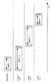
ここで、蓄積時間は、リセットしてから、信号を読み出す時までの期間である。そのため、全行の画素を一斉にリセットし、その後、1行づつ信号を出力していくと、行によって、蓄積時間が異なってくる。つまり、行が変わるごとに、蓄積時間が増えていくことになる。出力信号は、被写体の光の強さと、蓄積時間との積によって変化する。よって、出力信号値は、徐々に大きくなっていく。この時の出力信号の推移を、図10に示す。
【0087】
ただし、ここでの試行撮像時においては、全面に均一な光が照射されているものとする。よって、同じ行の画素であれば、同じ出力信号値になっている。
【0088】
1行目での出力信号値は、まだ小さい。そして、行が増え、k行目でも、まだ出力信号値は、飽和していない。そして、m行目になると、飽和する直前になる。さらに、行番号が大きくなると、出力信号が変化しなくなり、飽和してしまう。
【0089】
図10から、m行目の信号における蓄積時間が、最適であることが分かる。このような試行撮像動作により、最適な蓄積時間を容易に、かつ、素早く求めることが出来る。
【0090】
その後は、通常の撮像を行えばよい。ただし、この時の蓄積時間は、試行撮像によって求めた値を用いる。
【0091】
なお、本実施の形態は、MOS型パッシブセンサに適用することも出来る。ただし、CCD型センサは、一括リセット・一括読み出しであるので、本実施の形態を適用することは出来ない。
【0092】
なお、試行撮像時に、光が均一に照射されていなくてもよい。
【0093】
なお、MOS型センサでは、ランダムリセット・ランダム読み出しが出来るため、試行撮像時に、画面の一部のみから信号を出力させてもよい。
【0094】
なお、1行づつ蓄積時間を変える場合は、その行の画素の全てから信号を出力する必要は無い。すくなくとも、1行につき1画素から、信号を出力すればよい。
【実施例】
[実施例1]
次に、周辺に駆動回路を搭載し、画素を2次元に配置したエリアセンサでの実施例について述べる。全体の回路図を図11に示す。まず、画素が2次元に配列された撮像部1105がある。そして、各々の画素のゲート信号線やリセット信号線を駆動するための駆動回路が、撮像部1105の左右に配置されている。図11では、ゲート信号線用駆動回路1106が左側に、リセット信号線用駆動回路1107が右側に配置されている。
【0095】
そして、撮像部1105の上側には、信号処理用の回路などが配置されている。図11では、撮像部1105の上に、バイアス用回路1103が配置されている。このバイアス用回路1103は、各画素の増幅用トランジスタと対になって、ソースフォロワ回路を形成する。バイアス用回路1103の上には、サンプルホールド&信号処理用回路1102が配置されている。ここでは、信号をいったん保存しておいたり、アナログ・デジタル変換を行ったり、雑音を低減したりするための回路などが配置されている。サンプルホールド&信号処理用回路1102の上には、信号出力線用駆動回路1101が配置されている。信号出力線用駆動回路1101は、一時的に保存されていた信号を、順に出力していくための信号を出力している。そして、外に信号を出す前に、最終出力増幅用回路1104が配置されている。ここでは、サンプルホールド&信号処理用回路1102と信号出力線用駆動回路1101とにより、順に出力されてくる信号を、外に出す前に、増幅している。よって、信号を増幅しない場合は必要ないが、現実的には、配置されることが多い。
【0096】
次に、各部分の回路図を示す。まず、2次元に配列されている撮像部1105の中から、例として、i行j列目画素部回路1108の回路図を、図12に示す。図12では、Pチャネル型リセット用トランジスタ1207、Pチャネル型スイッチ用トランジスタ1201、Nチャネル型増幅用トランジスタ1206、光電変換素子(ここでは、最も代表的なフォトダイオード1204)から構成されている。フォトダイオード1204では、Pチャネル側端子は電源基準線1212に、Nチャネル側端子は、増幅用トランジスタ1206のゲート端子に接続されている。リセット用トランジスタ1207のゲート端子には、i行目リセット信号線1205が接続され、ソース端子とドレイン端子は、j列目電源線1209と増幅用トランジスタ1206のゲート端子に接続されている。スイッチ用トランジスタ1201のゲート端子は、i行目ゲート信号線1202に接続され、ソース端子とドレイン端子は、 j列目電源線1209と増幅用トランジスタ1206に接続されている。増幅用トランジスタ1206のソース端子とドレイン端子は、j列目信号出力線1203とスイッチ用トランジスタ1201に接続されている。
【0097】
図12では、リセット用トランジスタ1207は、Pチャネル型を用いている。しかし、リセット用トランジスタは、Nチャネル型でもよい。ただし、Nチャネル型の場合、リセット動作のとき、ゲート・ソース間電圧が大きくとれない。よって、リセット用トランジスタが飽和領域で動作することになり、フォトダイオード1204を十分に充電できない。したがって、リセット用トランジスタは、Nチャネル型でも動作するが、Pチャネル型の方が望ましい。
【0098】
スイッチ用トランジスタ1201については、j列目電源線1209と増幅用トランジスタ1206の間に配置し、かつ、Pチャネル型を用いるのが望ましい。しかし、従来と同様、Nチャネル型でも動作するため、Nチャネル型でも構わないし、j列目信号出力線1203と増幅用トランジスタ1206の間に配置しても構わない。ただし、正しく信号を出力しにくいため、スイッチ用トランジスタ1201は、j列目電源線1209と増幅用トランジスタ1206の間に配置し、かつ、Pチャネル型を用いるのが望ましい。
【0099】
増幅用トランジスタ1206については、図12では、Nチャネル型を用いている。しかし、Pチャネル型を用いることも可能である。ただしその場合、バイアス用トランジスタと組み合わせてソースフォロワ回路として動作させるためには、回路の接続方法を変える必要がある。つまり、単純に、図12の回路図において、増幅用トランジスタ1206の極性を変えるだけでは、動作しない。
【0100】
そこで、 Pチャネル型の増幅用トランジスタを用いた時の回路構成の一例を図13に示す。図12との違いは、増幅用トランジスタ1306の極性がPチャネル型であることと、フォトダイオードの向きが逆になっていることと、電源線と電源基準線とが入れ替わっていることである。増幅用トランジスタにPチャネル型を用いる場合は、バイアス用トランジスタもPチャネル型を用いる必要がある。なぜなら、バイアス用トランジスタは、定電流源として動作させる必要があるからである。よって、図13では、参考のため、バイアス用トランジスタ1311も記述している。図13に示すi行j列画素部回路1108は、Nチャネル型リセット用トランジスタ1307、Nチャネル型スイッチ用トランジスタ1301、Pチャネル型増幅用トランジスタ1306、光電変換素子(ここでは、最も代表的なフォトダイオード1304)から構成されている。フォトダイオード1304は、Nチャネル側端子は電源線1309に、Pチャネル側端子は、増幅用トランジスタ1306のゲート端子に接続されている。リセット用トランジスタ1307のゲート端子には、i行目リセット信号線1305が接続され、ソース端子とドレイン端子は、j列目電源基準線1312と増幅用トランジスタ1306のゲート端子に接続されている。スイッチ用トランジスタ1301のゲート端子は、i行目ゲート信号線1302に接続され、ソース端子とドレイン端子は、j列目電源基準線1312と増幅用トランジスタ1306に接続されている。増幅用トランジスタ1306のソース端子とドレイン端子は、j列目信号出力線1303とスイッチ用トランジスタ1301に接続されている。バイアス用トランジスタ1311のゲート端子には、バイアス信号線1310が接続され、ソース端子とドレイン端子は、j列目信号出力線1303と電源線1309に接続されている。
【0101】
図13では、リセット用トランジスタ1307は、Nチャネル型を用いている。しかし、リセット用トランジスタは、Pチャネル型でもよい。ただし、Pチャネル型の場合、リセット動作のとき、ゲート・ソース間電圧が大きくとれない。よって、リセット用トランジスタが飽和領域で動作することになり、フォトダイオード1304を十分に充電できない。したがって、リセット用トランジスタは、Pチャネル型でも動作するが、Nチャネル型の方が望ましい。
【0102】
図13では、スイッチ用トランジスタ1301については、 j列目電源基準線1312と増幅用トランジスタ1306の間に配置し、かつ、Nチャネル型を用いるのが望ましい。しかし、Pチャネル型でも動作するため、Pチャネル型でも構わないし、j列目信号出力線1303と増幅用トランジスタ1306の間に配置しても構わない。ただし、正しく信号を出力しにくいため、スイッチ用トランジスタ1301は、 j列目電源基準線1309と増幅用トランジスタ1306の間に配置し、かつ、Nチャネル型を用いるのが望ましい。
【0103】
このように、図12と図13を比較すると分かるように、増幅用トランジスタの極性が異なると、最適なトランジスタの構成、フォトダイオードの向きなども異なってくる。
【0104】
図12では、スイッチ用トランジスタ1201とリセット用トランジスタ1207の両方に、1本の電源線から電流を供給している。図13では、スイッチ用トランジスタ1301とリセット用トランジスタ1307の両方に、1本の電源基準線から電流を供給している。このように、フォトダイオードの向きと増幅用トランジスタの極性を合わせることにより、配線を共有出来る。
【0105】
次に、バイアス用回路1103とサンプルホールド&信号処理用回路1102の中から、1列分の回路として、j列目周辺部回路1109の回路図を、図14に示す。バイアス用回路1103には、バイアス用トランジスタ1411が配置されている。その極性は、各画素の増幅用トランジスタの極性と同じものである。よって、画素の増幅用トランジスタがNチャネル型の場合は、バイアス用トランジスタもNチャネル型になる。図14では、バイアス用トランジスタ1411は、Nチャネル型である。バイアス用トランジスタ1411のゲート端子には、バイアス信号線1410が接続され、ソース端子とドレイン端子は、j列目信号出力線1403と電源基準線1412に接続されている(バイアス用トランジスタがPチャネル型の場合は、電源基準線の代わりに、電源線を用いる)。バイアス用トランジスタ1411は、各画素の増幅用トランジスタと対になって、ソースフォロワ回路として動作する。転送用トランジスタ1413のゲート端子には、転送信号線1414が接続され、ソース端子とドレイン端子は、j列目信号出力線1403と負荷容量1415に接続されている。転送用トランジスタは、信号出力線1403の電位を負荷容量1415に転送するときに、動作させる。よって、Pチャネル型の転送用トランジスタを追加して、Nチャネル型転送用トランジスタ1414と並列に接続してもよい。負荷容量1415は、転送用トランジスタ1413と電源基準線1412に接続されている。負荷容量1415の役割は、信号出力線1403から出力される信号を一時的に蓄積することである。放電用トランジスタ1416のゲート端子は、プリ放電信号線1417に接続され、ソース端子とドレイン端子は、負荷容量1415と電源基準線1412に接続されている。放電用トランジスタ1416は、信号出力線1403の電位を負荷容量1415に入力する前に、いったん、負荷容量1415にたまっている電荷を放電するように動作する。
【0106】
なお、アナログ・デジタル信号変換回路や雑音低減回路などを配置することも可能である。
【0107】
そして、負荷容量1415と最終出力線1420の間に、最終選択用トランジスタ1419が接続される。最終選択用トランジスタ1419のソース端子とドレイン端子は、負荷容量1415と最終出力線1420に接続され、ゲート端子は、j列目最終選択線1418に接続される。最終選択線は、1列目から順にスキャンされる。そして、j列目最終選択線1418が選択され、最終選択用トランジスタ1419が導通状態になると、負荷容量1415の電位と最終出力線1420の電位が等しくなる。その結果、負荷容量1415に蓄積していた信号を最終出力線1420に出力することが出来る。ただし、最終出力線1420に信号を出力する前に、最終出力線1420に電荷が蓄積されていると、その電荷により、最終出力線1420に信号を出力したときの電位が影響を受けてしまう。そこで、最終出力線1420に信号を出力するまえに、最終出力線1420の電位を、ある電位値に初期化しなければならない。図14では、最終出力線1420と電源基準線1412の間に、最終リセット用トランジスタ1422を配置している。そして、最終リセット用トランジスタ1422のゲート端子には、j列目最終リセット線1421が接続されている。そして、j列目最終選択線1418を選択する前に、j列目最終リセット線1421を選択し、最終出力線1420の電位を電源基準線1412の電位に初期化する。その後、j列目最終選択線1418を選択し、最終出力線1420に、負荷容量1415に蓄積していた信号を出力する。
【0108】
最終出力線1420に出力される信号は、そのまま外に取り出しても良い。しかしながら、信号が微弱であるため、外に取り出す前に、信号を増幅しておく場合が多い。そのための回路として、図15に、最終部回路1110の回路を示す。信号を増幅する回路としては、演算増幅器など、様々なものがある。信号を増幅する回路であれば、どのような回路でもよいが、ここでは、最も簡単な回路構成として、ソースフォロワ回路を示す。図15では、Nチャネル型の場合を示す。最終出力増幅用回路1104への入力は、最終出力線1502となる。最終出力線1502には、1列目から順に、信号が出力される。その信号を、最終出力増幅用回路1104によって、増幅し、外に出力する。最終出力線1502は、最終出力増幅向け増幅用トランジスタ1504のゲート端子に接続される。最終出力増幅向け増幅用トランジスタ1504のドレイン端子は、電源線1506に接続され、ソース端子は、出力端子となる。最終出力増幅向けバイアス用トランジスタ1503のゲート端子は、最終出力増幅用バイアス信号線1505と接続される。ソース端子とドレイン端子は、電源基準線1507と最終出力増幅向け増幅用トランジスタ1504のソース端子とに接続される。
【0109】
図16に、Pチャネル型の場合のソースフォロワ回路を用いた場合の回路図を示す。図15との違いは、電源線と電源基準線を逆にしていることである。最終出力線1602は、最終出力増幅向け増幅用トランジスタ1604のゲート端子に接続される。最終出力増幅向け増幅用トランジスタ1604のドレイン端子は、電源基準線1607に接続され、ソース端子は、出力端子となる。最終出力増幅向けバイアス用トランジスタ1603のゲート端子は、最終出力増幅用バイアス信号線1605と接続される。ソース端子とドレイン端子は、電源線1606と最終出力増幅向け増幅用トランジスタ1604のソース端子とに接続される。最終出力増幅用バイアス信号線1605の電位は、Nチャネル型を用いた場合の最終出力増幅用バイアス信号線1505とは、値が異なる。
【0110】
図15と図16では、ソースフォロワ回路を1段のみで構成していた。しかしながら、複数段で構成しても良い。例えば、2段で構成する場合は、1段目の出力端子を2段目の入力端子に接続すればよい。また、各々の段において、Nチャネル型を用いても、Pチャネル型を用いても、どちらでも良い。
【0111】
ゲート信号線用駆動回路1106やリセット信号線駆動回路1107や信号出力線用駆動回路1101は、単に、パルス信号を出力しているだけの回路である。よって、公知の技術を用いて実施出来る。
【0112】
次に、試行撮像を行う時のタイミングチャートについて述べる。図17に、図11と図12の回路におけるタイミングチャートを示す。まず、全行のリセット信号線を制御して、画素を同時にリセットする。その後、ゲート信号線は、1行目から順にスキャンしていく。例えば、(i-1)行目を選択し、その次に、i行目を選択し、次に、(i+1)行目を選択していく。そして、最後の行までスキャンしたら、再び同じ1行目からスキャンし、同様の動作を繰り返していく。
【0113】
画素がリセットされてから、ゲート信号線が選択されて、信号を出力する時までの期間が、蓄積時間になる。蓄積時間の間、フォトダイオードにおいて、光によって生成される電荷を蓄積している。各行で、リセットされるタイミングは同じで、信号を出力するタイミングは、異なる。よって、蓄積時間は行ごとに異なってくる。
【0114】
次に、図14における信号のタイミングチャートを図18に示す。繰り返しの動作になるため、例として、i行目のゲート信号線が選択されている時を考える。まず、i行目のゲート信号線1202が選択された後、プリ放電信号線1417を選択し、放電用トランジスタ1416を導通状態にする。その後、転送信号線1414を選択する。すると、i行目の画素から、各列の信号が各列の負荷容量1415に出力される。
【0115】
i行目の全ての画素の信号を、各列の負荷容量1415に蓄積した後、最終出力線1420に各列の信号を順に出力していく。転送信号線1414が非選択になってから、ゲート信号線が選択されているまでの間、信号出力線用駆動回路1101により、全列をスキャンしていく。まず、1列目の最終リセット線を選択し、最終リセット用トランジスタ1422を導通状態にし、最終出力線1420を電源基準線1412の電位に初期化する。その後、1列目の最終選択線1418を選択し、最終選択用トランジスタ1419を導通状態にし、1列目の負荷容量1415の信号を最終出力線1420に出力する。つぎに、2列目の最終リセット線を選択し、最終リセット用トランジスタ1422を導通状態にし、最終出力線1420を電源基準線1412の電位に初期化する。その後、2列目の最終選択線1418を選択し、最終選択用トランジスタ1419を導通状態にし、2列目の負荷容量1415の信号を最終出力線1420に出力する。その後も、同様の動作を繰り返していく。j列目の場合も、j列目の最終リセット線を選択し、最終リセット用トランジスタ1422を導通状態にし、最終出力線1420を電源基準線1412の電位に初期化する。その後、j列目の最終選択線1418を選択し、最終選択用トランジスタ1419を導通状態にし、j列目の負荷容量1415の信号を最終出力線1420に出力する。つぎに、(j+1)列目の最終リセット線を選択し、最終リセット用トランジスタ1422を導通状態にし、最終出力線1420を電源基準線1412の電位に初期化する。その後、(j+1)列目の最終選択線1418を選択し、最終選択用トランジスタ1419を導通状態にし、(j+1)列目の負荷容量1415の信号を最終出力線1420に出力する。その後も、同様の動作を繰り返し、全列の信号を最終出力線に、順次、出力していく。そのあいだ、バイアス信号線1410は、一定のままである。最終出力線1420に出力された信号は、最終出力増幅用回路1104で増幅され、外へ出力されていく。
【0116】
次に、i+1行目ゲート信号線が選択される。すろと、i行目ゲート信号線が選択されたのと同様に、動作させる。そして、さらに、次の行のゲート信号線が選択され、同様の動作を繰り返していく。
【0117】
全画面に均一な光が照射されている場合の出力信号(最終出力増幅用回路1104からの出力)が、行ごとに変わっていく図は、図19のようになる。ただし、同じ行の画素からは、同じ値の出力信号が出力されるため、行毎に1つの出力信号のみを示している。
【0118】
まず、1行目からの出力信号は、蓄積時間が小さいため、値が小さい。それから、行番号が大きくなると、出力信号も大きくなってくる。そして、全行から信号を出力し終わっても、まだ、信号が飽和していなかったとする。その場合、再び、1行目から信号を出力していく。そして、2回目の読み出し時のm行目の画素の直後に、信号が飽和し始めたとする。すると、これから、2回目の読み出し時のm行目の画素における蓄積時間を、最適な蓄積時間とする事が出来る。
【0119】
以上のような試行撮像により、最適な蓄積時間を、容易に、かつ素早く求めることが出来る。
【0120】
その後、最適な蓄積時間に設定し、通常の撮像を行えばよい。動作において、通常の撮像と試行撮像の違いは、リセットするタイミングだけである。そこで、通常の撮像の時の信号タイミングチャートを以下に示す。
【0121】
まず、図11と図12の回路におけるタイミングチャートについて、図20に示す。リセット信号線は、1行目から順にスキャンしていく。例えば、(i-1)行目を選択し、その次に、i行目を選択し、次に、(i+1)行目を選択していく。再び同じ行を選択するまでの期間がフレーム期間に相当する。ゲート信号線も、同様に、1行目から順にスキャンしていく。ただし、リセット信号線をスキャンし始めるタイミングよりも、ゲート信号線をスキャンし始めるタイミングの方が遅い。例えば、i行目の画素に着目すると、i行目リセット信号線が選択されて、その後、i行目ゲート信号線が選択される。i行目ゲート信号線が選択されると、i行目の画素から信号が出力される。画素がリセットされてから、信号を出力する時までの期間が、蓄積時間になる。蓄積時間の間、フォトダイオードにおいて、光によって生成される電荷を蓄積している。各行で、リセットされるタイミングと信号を出力するタイミングは、異なる。よって、蓄積時間は全行の画素で等しいが、蓄積する時刻は異なる。
【0122】
図14における信号のタイミングチャートは、図18と同じである。
【0123】
このように、リセット信号線を制御するタイミングを変えるだけで、簡単に試行撮像と通常の撮像を切り替えて行うことが出来る。
【0124】
このような動作は、MOS型アクティブセンサが、ランダムリセット・ランダム読み出しが可能であり、非破壊的読み出しが出来るため、可能となる。CCD型センサでは、実現できない。
【0125】
なお、MOS型パッシブセンサにおいても、適用することが出来る。ただし、破壊的読み出しであるため、試行撮像において、2回目以降の信号読み出しは、実行出来ない。そのため、1回のスキャンで最適な蓄積時間を探せるようにする必要がある。その場合は、リセットしてから、1行目の信号を出力する時間を調節して、試行撮像を行えばよい。なお、リセットしてから、1行目の信号を出力する時間の調節は、MOS型アクティブセンサの場合にも行ってもよい。
【0126】
なお、光電変換などを行うセンサ部については、通常のPN型のフォトダイオードの他に、PIN型のダイオード、アバランシェ型ダイオード、npn埋め込み型ダイオード、ショットキー型ダイオード、X線用のフォトコンダクタ、赤外線用のセンサなどでもよい。また、蛍光材やシンチレータにより、X線を光に変換した後、その光を読みとってもよい。
【0127】
これまで述べてきたように、光電変換素子は、ソースフォロワ回路の入力端子に接続されることが多い。しかし、フォトゲート型のように、スイッチを間に挟んでもよい。あるいは、対数変換型のように、光強度の対数値なるように処理した後の信号を入力端子に入力してもよい。
【0128】
なお、本実施例では、画素が2次元に配置されたエリアセンサについて述べたが、画素が1次元に配置されたラインセンサを実現することも出来る。
【0129】
本実施例のように、試行撮像において、均一な光を照射するということは、例えば、スキャナでの試行撮像において適用することが出来る。つまり、実際の原稿を撮像するまえに、補正用で全面が白の原稿を用いて、試行撮像を行う場合に、適用することが出来る。例えば、スキャナの光源の光強度が不明な場合、本実施例を適用すれば、最適な蓄積時間を、容易にすばやく、見つけることが出来るようになる。そして、通常の撮像を実際の原稿に対して行えば、精度よく読み取ることが出来る。
【0130】
[実施例2]
実施例1では、試行撮像の時、全面に均一な光が照射されている場合について述べた。ここでは、試行撮像の時、全面に不均一な光が照射されている場合について述べる。
【0131】
しかしながら、動作、回路など、実施例1とほとんど同じである。ただし、全面に不均一な光が照射されているため、同じ行の画素であっても、つまり、同じ蓄積時間の画素であっても、信号値が異なってくる。そのため、図19のように、行番号に対する信号値の推移のグラフを示す場合、ある行における出力信号値として、どの値を用いればよいか分からない。
【0132】
このような場合は、各々の行において、最も出力信号振幅値が大きいもの(最も光強度が強い場合に相当)を用いて、図19のようなグラフを示せばよい。そうすれば、その他の全ては、実施例1の場合と同じようになる。
【0133】
本実施例のように、試行撮像において、不均一な光を照射するということは、例えば、全体が黒っぽいような原稿(新聞など)を読み取る時に適用することが出来る。このような原稿を読み取る場合、文字部分とそれ以外の部分との階調差が少ないため、正確に読み取ることが難しい。
【0134】
そこで、その様な場合、実際に読み取る原稿を用いて、まず試行撮像を行う。この場合は、全面に不均一な光がセンサに照射されることになる。このような場合において、図10のように、行番号に対する信号値の推移のグラフを、図21に示す。各行における出力信号振幅値は、最も大きい値を用いる。最も大きい出力信号振幅値は、最も明るい場合に相当する。図21では、全面が黒っぽい原稿を読み取る場合は、3回目のn行目の時の蓄積時間が最適であることが分かる。この時の蓄積時間をTs1とする。
【0135】
仮に、画面全体が白い原稿を用いて試行撮像をする場合は、図21に示すように、2回目のm行目の時の蓄積時間が最適であることが分かる。この時の蓄積時間をTs2とする。
【0136】
もし、通常の原稿を読み取る場合は、蓄積時間は、Ts2に設定して撮像を行うのがよい。しかし、新聞のような黒っぽい原稿を読み取る場合は、蓄積時間をTs1に設定しなおして、撮像を行う方がよい。その方が、信号の振幅が大きくなり、読み取り精度が向上する。
【0137】
このように、読み取り原稿のタイプによって、蓄積時間を設定しなおすと、よりきれいな画像で読み取ることが出来るようになる。その時に設定しなおす最適時間は、実施例1や実施例2のような試行撮像を行えば、短時間で簡単に見つけることが出来る。
【0138】
[実施例3]
実施例1、実施例2では、試行撮像の時、全面の画素から信号を出力していた。しかしながら、画面のある領域のみを対象として、試行撮像を行っても良い。よって、本実施例は、実施例1や実施例2と自由に組み合わせることが出来る。
【0139】
図22に示すように、画素のr行目からs行目まで、t列目からu列目まで、の領域を対象として、試行撮像を行うとする。
【0140】
この時の信号タイミングチャートは、次のようになる。まず、試行撮像する対象の領域に含まれる画素の全てを同時にリセットする。ただし、それ以外の領域の画素もリセットしても構わない。その後、r行目から信号を出力していく。つまり、リセットした後、r行目から信号を出力しはじめる。1行目から信号を出力しはじめるのではない。
【0141】
画素から信号が出力されるとき、1行分同時に画素から出力されるが、実際に必要なのは、t列目からu列目までの信号である。よって、それ以外の信号は、信号出力線用駆動回路1101での波形を制御して、最終出力増幅用回路1104から外へ出力しないようにしてもよい。あるいは、1行分出力したのち、不必要な信号は、無視しても構わない。
【0142】
信号出力線用駆動回路1101での波形を制御する場合は、公知の回路や信号を用いれば、実現出来る。
【0143】
次にゲート信号線をスキャンして、r+1行目から出力し、その次にr+2行目から出力し、・・・と繰り返す。そして、s行目まで出力したのちは、s+1行目に行くのではなく、またr行目に戻り、信号を出力する。そして、r+1行目にスキャンし、・・・と繰り返していく。
【0144】
このようにすれば、行毎に蓄積時間が徐々に長くなっていく。s行目まで出力したのち、またr行目に戻りスキャンすることにより、蓄積時間が不連続になることを防ぐことが出来る。
【0145】
このようにゲート信号線を制御するためには、ゲート信号線用駆動回路1106において、公知の回路や信号を用いれば、実現出来る。
【0146】
このように、自由に信号を読み出せるのは、MOS型センサがランダムリセット・ランダム読み出し方式だからである。CCD型センサでは、実現出来ない。
【0147】
本実施例のように、試行撮像において、決まった領域のみを対象とするということは、例えば、画面の中心部にのみ撮像したいものからの光が入射し、画面の周辺部には、無関係な光が入射するような場合に適用することが出来る。例としては、指紋の読み取りが挙げられる。
【0148】
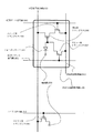
そこで、図23に、画面に指を押しつけて、指紋を読み取る場合の模式図を示す。図23(A)は、上から見た図であり、図23(B)は、断面図である。画素配列2301があり、ここに、たくさんの画素が配置されている。撮像できる領域は、画素配列2301の全領域である。その上に、読み取り対象物2302である指を置く。しかしながら、実際に指が押しつけられているのは、撮像対象領域2303の部分だけであり、撮像非対象領域2304には、何もない。よって、撮像非対象領域2304には、周囲の光などの雑音が入ってしまう。その様な場合、画面全体を対象として試行撮像を行うと、正しい蓄積時間を見つけることが出来ない。そのため、試行撮像は、指が押しつけられている領域に対して行う。
【0149】
また、指紋を読み取る場合、指紋の凹凸部分の階調が近い。そのため、正確に読み取ることが難しい。図24に、指紋読み取りの場合の画素のフォトダイオードのNチャネル側端子の電位のタイミングチャートを示す。まず、画素をリセットする。その後、光強度に応じて、フォトダイオードのNチャネル側端子の電位が低くなってくる。黒い原稿を読み取る場合は、電位はほとんど低くならず、白い原稿を読み取る場合は、電位が大きく低下する。通常の場合は、白い原稿を読み取るときに信号が飽和しないように、蓄積時間を設定する。しかし、指紋を読み取る場合は、指紋の凹凸部分の階調が近いため、フォトダイオードのNチャネル側端子の電位も近い。よって、指紋の凹凸部分を正確に読み取ることが難しい。
【0150】
このような場合、指が押しつけられている領域のみを対象として、指を押しつけて、試行撮像に行う。この場合、試行撮像を行うときには、不均一な光がセンサに照射されている。そして、最も明るい部分の信号(最も大きな信号振幅)が飽和する直前までの期間を最適な蓄積時間とする。
【0151】
そして通常の撮像を行うと、フォトダイオードのNチャネル側端子の電位は大きく低下し、その結果、指紋を読み取るときの凹凸部分の信号の電位差が、大きくなる。そのため、階調の差を検出しやすくなり、指紋のような階調差が小さい画像でも読み取ることが出来るようになる。
【0152】
[実施例4]
本願発明のセンサを、 TFTを用いてガラス上に作製する場合の作製方法について、図26〜図29を用いて説明する。
【0153】
まず、図26(A)に示すように、ガラス基板200上に下地膜201を300nmの厚さに形成する。本実施例では下地膜201として窒化酸化珪素膜を積層して用いる。この時、ガラス基板200に接する方の窒素濃度を10〜25wt%としておくと良い。また、下地膜201に放熱効果を持たせることは有効であり、DLC(ダイヤモンドライクカーボン)膜を設けても良い。
【0154】
次に下地膜201の上に50nmの厚さの非晶質珪素膜(図示せず))を公知の成膜法で形成する。なお、非晶質珪素膜に限定する必要はなく、非晶質構造を含む半導体膜(微結晶半導体膜を含む)であれば良い。さらに非晶質シリコンゲルマニウム膜などの非晶質構造を含む化合物半導体膜でも良い。また、膜厚は20〜100nmの厚さであれば良い。
【0155】
そして、公知の技術により非晶質珪素膜を結晶化し、結晶質珪素膜(多結晶シリコン膜若しくはポリシリコン膜ともいう)202を形成する。公知の結晶化方法としては、電熱炉を使用した熱結晶化方法、レーザー光を用いたレーザーアニール結晶化法、赤外光を用いたランプアニール結晶化法がある。本実施例では、XeClガスを用いたエキシマレーザー光を用いて結晶化する。
【0156】
なお、本実施例では線状に加工したパルス発振型のエキシマレーザー光を用いるが、矩形であっても良いし、連続発振型のアルゴンレーザー光や連続発振型のエキシマレーザー光を用いることもできる。
【0157】
また、本実施例では結晶質珪素膜をTFTの活性層として用いるが、非晶質珪素膜を用いることも可能である。
【0158】
なお、オフ電流を低減する必要のあるリセット用トランジスタの活性層を非晶質珪素膜で形成し、増幅用トランジスタの活性層を結晶質珪素膜で形成することは有効である。非晶質珪素膜はキャリア移動度が低いため電流を流しにくくオフ電流が流れにくい。即ち、電流を流しにくい非晶質珪素膜と電流を流しやすい結晶質珪素膜の両者の利点を生かすことができる。
【0159】
次に、図26(B)に示すように、結晶質珪素膜202上に酸化珪素膜でなる保護膜203を130nmの厚さに形成する。この厚さは100〜200nm(好ましくは130〜170nm)の範囲で選べば良い。また、珪素を含む絶縁膜であれば他の膜でも良い。この保護膜203は不純物を添加する際に結晶質珪素膜が直接プラズマに曝されないようにするためと、微妙な濃度制御を可能にするために設ける。
【0160】
そして、その上にレジストマスク204a、204b、204cを形成し、保護膜203を介してn型を付与する不純物元素(以下、n型不純物元素という)を添加する。なお、n型不純物元素としては、代表的には周期表の15族に属する元素、典型的にはリン又は砒素を用いることができる。なお、本実施例ではフォスフィン(PH3)を質量分離しないでプラズマ励起したプラズマドーピング法を用い、リンを1×10¹⁸atoms/cm3の濃度で添加する。勿論、質量分離を行うイオンインプランテーション法を用いても良い。
【0161】
この工程により形成されるn型不純物領域(b)205a、205bには、n型不純物元素が2×10¹⁶〜5×10¹⁹atoms/cm3(代表的には5×1017〜5×1018atoms/cm3)の濃度で含まれるようにドーズ量を調節する。
【0162】
次に、図26(C)に示すように、保護膜203、レジストマスク204a、204b、204cを除去し、添加したn型不純物元素の活性化を行う。活性化手段は公知の技術を用いれば良いが、本実施例ではエキシマレーザー光の照射(レーザーアニール)により活性化する。勿論、パルス発振型でも連続発振型でも良いし、エキシマレーザー光に限定する必要はない。但し、添加された不純物元素の活性化が目的であるので、結晶質珪素膜が溶融しない程度のエネルギーで照射することが好ましい。なお、保護膜203をつけたままレーザー光を照射しても良い。
【0163】
なお、このレーザー光による不純物元素の活性化に際して、熱処理(ファーネスアニール)による活性化を併用しても構わない。熱処理による活性化を行う場合は、基板の耐熱性を考慮して450〜550℃程度の熱処理を行えば良い。
【0164】
この工程によりn型不純物領域(b)205a、205bの端部、即ち、n型不純物領域(b)205a、205bの周囲に存在するn型不純物元素を添加していない領域との境界部(接合部)が明確になる。このことは、後にTFTが完成した時点において、LDD領域とチャネル形成領域とが非常に良好な接合部を形成しうることを意味する。
【0165】
次に、図26(D)に示すように、結晶質珪素膜の不要な部分を除去して、島状の半導体膜(以下、活性層という)206〜210を形成する。
【0166】
次に、図27(A)に示すように、活性層206〜210を覆ってゲート絶縁膜211を形成する。ゲート絶縁膜211としては、10〜200nm、好ましくは50〜150nmの厚さの珪素を含む絶縁膜を用いれば良い。これは単層構造でも積層構造でも良い。本実施例では110nm厚の窒化酸化珪素膜を用いる。
【0167】
次に、200〜400nm厚の導電膜を形成し、パターニングしてゲート電極212〜216を形成する。なお本実施例では、ゲート電極とゲート電極に電気的に接続された引き回しのための配線(以下、ゲート配線という)とを同一材料で形成している。勿論、ゲート電極と、ゲート配線とを別の材料で形成しても良い。具体的にはゲート電極よりも低抵抗な材料をゲート配線として用いても良い。これは、ゲート電極としては微細加工が可能な材料を用い、ゲート配線には微細加工はできなくとも配線抵抗が小さい材料を用いるためである。このような構造とすることでゲート配線の配線抵抗を非常に小さくすることができるため、面積の大きいセンサ部を形成することができる。即ち、画面の大きさが対角10インチ以上(さらには30インチ以上)のセンサ部を有するエリアセンサを実現する上で、上記の画素構造は極めて有効である。
【0168】
また、ゲート電極は単層の導電膜で形成しても良いが、必要に応じて二層、三層といった積層膜とすることが好ましい。ゲート電極212〜216の材料としては公知のあらゆる導電膜を用いることができる。
【0169】
代表的には、アルミニウム(Al)、タンタル(Ta)、チタン(Ti)、モリブデン(Mo)、タングステン(W)、クロム(Cr)、シリコン(Si)から選ばれた元素でなる膜、または前記元素の窒化物膜(代表的には窒化タンタル膜、窒化タングステン膜、窒化チタン膜)、または前記元素を組み合わせた合金膜(代表的にはMo−W合金、Mo−Ta合金)、または前記元素のシリサイド膜(代表的にはタングステンシリサイド膜、チタンシリサイド膜)を用いることができる。勿論、単層で用いても積層して用いても良い。
【0170】
本実施例では、30nm厚の窒化タングステン(WN)膜と、370nm厚のタングステン(W)膜とでなる積層膜を用いる。これはスパッタ法で形成すれば良い。また、スパッタガスとしてXe、Ne等の不活性ガスを添加すると応力による膜はがれを防止することができる。
【0171】
またこの時、ゲート電極213、216はそれぞれn型不純物領域(b)205a、205bの一部とゲート絶縁膜211を介して重なるように形成する。この重なった部分が後にゲート電極と重なったLDD領域となる。
【0172】
次に、図27(B)に示すように、ゲート電極212〜216をマスクとして自己整合的にn型不純物元素(本実施例ではリン)を添加する。こうして形成されるn型不純物領域(c)217〜224にはn型不純物領域(b)205a、205bの1/2〜1/10(代表的には1/3〜1/4)の濃度でリンが添加されるように調節する。具体的には、1×1016〜5×1018atoms/cm3(典型的には3×1017〜3×1018atoms/cm3)の濃度が好ましい。
【0173】
次に、図27(C)に示すように、ゲート電極212、214、215を覆う形でレジストマスク225a〜225cを形成し、n型不純物元素(本実施例ではリン)を添加して高濃度にリンを含むn型不純物領域(a)226〜233を形成する。ここでもフォスフィン(PH3)を用いたイオンドープ法で行い、この領域のリンの濃度は1×10²⁰〜1×10²¹atoms/cm3(代表的には2×1020〜5×1021atoms/cm3)となるように調節する。
【0174】
この工程によってnチャネル型TFTのソース領域若しくはドレイン領域が形成される。そしてnチャネル型TFTでは、図27(B)の工程で形成したn型不純物領域217、218、222、223の一部を残す。この残された領域がLDD領域となる。
【0175】
次に、図27(D)に示すように、レジストマスク225a〜225cを除去し、新たにレジストマスク234a、234bを形成する。そして、p型不純物元素(本実施例ではボロン)を添加し、高濃度にボロンを含むp型不純物領域235、236を形成する。ここではジボラン(B2H6)を用いたイオンドープ法により3×10²⁰〜3×10²¹atoms/cm3(代表的には5×1020〜1×1021atoms/cm3ノ)濃度となるようにボロンを添加する。
【0176】
なお、不純物領域235、236には既に1×10²⁰〜1×10²¹atoms/cm3の濃度でリンが添加されているが、ここで添加されるボロンはその少なくとも3倍以上の濃度で添加される。そのため、予め形成されていたn型の不純物領域は完全にp型に反転し、p型の不純物領域として機能する。
【0177】
次に、レジストマスク234a、234bを除去した後、それぞれの濃度で添加されたn型またはp型不純物元素を活性化する。活性化手段としては、ファーネスアニール法、レーザーアニール法、またはランプアニール法で行うことができる。本実施例では電熱炉において窒素雰囲気中、550℃、4時間の熱処理を行う。
【0178】
このとき雰囲気中の酸素を極力排除することが重要である。なぜならば酸素が少しでも存在していると露呈したゲート電極の表面が酸化され、抵抗の増加を招くからである。従って、上記活性化工程における処理雰囲気中の酸素濃度は1ppm以下、好ましくは0.1ppm以下とすることが望ましい。
【0179】
次に、図28(A)に示すように、第1層間絶縁膜237を形成する。第1層間絶縁膜237としては、珪素を含む絶縁膜を単層で用いるか、その中で組み合わせた積層膜を用いれば良い。また、膜厚は400nm〜1.5μmとすれば良い。本実施例では、200nm厚の窒化酸化珪素膜の上に800nm厚の酸化珪素膜を積層した構造とする。
【0180】
さらに、3〜100%の水素を含む雰囲気中で、300〜450℃で1〜12時間の熱処理を行い水素化処理を行う。この工程は熱的に励起された水素により半導体膜の不対結合手を水素終端する工程である。水素化の他の手段として、プラズマ水素化(プラズマにより励起された水素を用いる)を行っても良い。
【0181】
なお、水素化処理は第1層間絶縁膜237を形成する間に入れても良い。即ち、200nm厚の窒化酸化珪素膜を形成した後で上記のように水素化処理を行い、その後で残り800nm厚の酸化珪素膜を形成しても構わない。
【0182】
次に、ゲート絶縁膜211及び第1層間絶縁膜237に対してコンタクトホールを形成し、ソース配線238〜242と、ドレイン配線243〜247を形成する。なお、本実施例ではこの電極を、Ti膜を100nm、Tiを含むアルミニウム膜を300nm、Ti膜150nmをスパッタ法で連続形成した3層構造の積層膜とする。勿論、他の導電膜でも良い。
【0183】
次に、50〜500nm(代表的には200〜300nm)の厚さで第1パッシベーション膜248を形成する。本実施例では第1パッシベーション膜248として300nm厚の窒化酸化珪素膜を用いる。これは窒化珪素膜で代用しても良い。なお、窒化酸化珪素膜の形成に先立ってH2、NH3等水素を含むガスを用いてプラズマ処理を行うことは有効である。この前処理により励起された水素が第1層間絶縁膜237に供給され、熱処理を行うことで、第1パッシベーション膜248の膜質が改善される。それと同時に、第1層間絶縁膜237に添加された水素が下層側に拡散するため、効果的に活性層を水素化することができる。
【0184】
次に、図28(B)に示すように有機樹脂からなる第2層間絶縁膜249を形成する。有機樹脂としてはポリイミド、ポリアミド、アクリル、BCB(ベンゾシクロブテン)等を使用することができる。特に、第2層間絶縁膜249は平坦化の意味合いが強いので、平坦性に優れたアクリルが好ましい。本実施例ではTFTによって形成される段差を十分に平坦化しうる膜厚でアクリル膜を形成する。好ましくは1〜5μm(さらに好ましくは2〜4μm)とすれば良い。
【0185】
次に、第2層間絶縁膜249及び第1パッシベーション膜248にドレイン配線245に達するコンタクトホールを形成し、ドレイン配線245に接するようにフォトダイオードのカソード電極250を形成する。本実施例では、カソード電極250としてスパッタ法によって形成したアルミニウム膜を用いたが、その他の金属、例えばチタン、タンタル、タングステン、銅を用いることができる。また、チタン、アルミニウム、チタンでなる積層膜を用いてもよい。
【0186】
次に、水素を含有する非晶質珪素膜を基板全面に成膜した後にパターニングし、光電変換層251を形成する。次に、基板全面に透明導電膜を形成する。本実施例では透明導電膜として厚さ200nmのITOをスパッタ法で成膜する。透明導電膜をパターニングし、アノード電極252を形成する。(図28(C))
【0187】
次に、図29(A)に示すように第3層間絶縁膜253を形成する。第3層間絶縁膜253として、ポリイミド、ポリアミド、ポリイミドアミド、アクリル等の樹脂を用いることで、平坦な表面を得ることができる。本実施例では、第3層間絶縁膜253として厚さ0.7μmのポリイミド膜を基板全面に形成した。
【0188】
次に、第3層間絶縁膜253に、アノード電極252に達するコンタクトホールを形成し、センサ用配線254を形成する。本実施例ではアルミニウム合金膜(1wt%のチタンを含有したアルミニウム膜)を300nmの厚さに形成する。
【0189】
こうして図29(B)に示すような構造のセンサ基板が完成する。
【0190】
270は増幅用TFT、271はスイッチ用TFT、272はリセット用TFT、273はバイアス用TFT、274は放電用TFTである。
【0191】
本実施例では、増幅用TFT270及びバイアス用TFT273がnチャネル型TFTであり、それぞれソース領域側とドレイン領域側の両方にそれぞれLDD領域281〜284を有している。なおこのLDD領域281〜284はゲート絶縁膜211を間に介してゲート電極212、215と重なっていない。上記構成により、増幅用TFT270及びバイアス用TFT273は、極力ホットキャリア注入を低減させることができる。
【0192】
また本実施例では、スイッチ用TFT271及び放電用TFT274がnチャネル型TFTであり、それぞれドレイン領域側にのみそれぞれLDD領域283、286を有している。なおこのLDD領域283、286はゲート絶縁膜211を間に介してゲート電極213、216と重なっている。
【0193】
ドレイン領域側のみにLDD領域283、286を形成しているのは、ホットキャリア注入を低減させ、なおかつ動作速度を落とさないための配慮である。また、このスイッチ用271及び放電用TFT274はオフ電流値をあまり気にする必要はなく、それよりも動作速度を重視した方が良い。従って、LDD領域283、286は完全にゲート電極213、216と重ねてしまい、極力抵抗成分を少なくすることが望ましい。即ち、いわゆるオフセットはなくした方がよい。特に、ソース信号線駆動回路又はゲート信号線駆動回路を15V〜20Vで駆動させる場合、本実施例の放電用TFT274の上記構成は、ホットキャリア注入を低減させ、なおかつ動作速度を落とさないのに有効である。
【0194】
また本実施例では、リセット用TFT272はpチャネル型TFTであり、LDD領域を有していない。pチャネル型TFTは、ホットキャリア注入による劣化が殆ど気にならないので、特にLDD領域を設けなくても良い。勿論、nチャネル型TFTと同様にLDD領域を設け、ホットキャリア対策を講じることも可能である。また、リセット用TFT272がnチャネル型TFTであっても良い。
【0195】
また、基板上に形成された素子又は回路から引き回された端子と外部信号端子とを接続するためのコネクター(フレキシブルプリントサーキット:FPC)を取り付けて製品として完成する。
【0196】
なお、実施例4は、実施例1〜実施例3と、自由に組み合わせることが出来る。
【0197】
なお、本願発明は、単結晶シリコン基板を用いて作成することも可能である。
【0198】
[実施例5]
本願発明を実施して形成されたセンサは、様々な電子機器に用いることが出来る。その様な本願発明の電子機器としては、スキャナ、デジタルスチルカメラ、X線カメラ、携帯情報端末(モバイルコンピュータ、携帯電話、携帯型ゲーム機)、ノート型パーソナルコンピュータ、ゲーム機器、テレビ電話、指紋読み取り機器等が挙げられる。
【0199】
図29(A)は、密着型センサを用いたスキャナ2901であり、センサ部2902等を含む。読み取り対象物2903の上にスキャナ2901を配置する。密着型センサは、ガラス基板上に、TFTを形成して、作成されている。密着型センサでは、縮小光学系を用いないため、機器を小型化できる。読み取り対象物2903に照射する光は、室内光を利用する。これにより、専用の光源が必要なくなる。この場合、光強度が、撮像環境により変化する。よって、本願発明を適用することによって、素早く最適な蓄積時間を見つけることが出来る。本願発明は、センサ部2902に用いることが出来る。
【0200】
図29(B)は、図29(A)に対して、専用の光源2907を配置したものである。読み取りたい領域とセンサ部2905の位置を合わせるときは、光源2907を上に上げておく。そして、センサ部2905の照明窓を通して、読み取り対象物2906を見て、位置を合わせる。画像を読み取る時は、光源2907とスキャナ2904を重ねて使用する。本願発明は、センサ部2905に用いることが出来る。
【0201】
図30(A)は、携帯情報端末3001であり、LCD3002、密着型センサを用いたスキャナ3003、センサ部3004等を含む。スキャナを使用する時は、図30(B)の断面図に示すように、LCD3002とスキャナ3003を重ねて、読み取り対象物2903の上にスキャナ2901を配置し、その上にLCD3002が配置されるようにする。照明光は、LCD3002の光を利用する。これにより、専用の光源が必要なくなる。本願発明は、センサ部2902に用いることが出来る。
【0202】
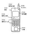
ここで図31は携帯電話であり、本体3101、音声出力部3102、音声入力部3103、表示装置3104、操作スイッチ3105、アンテナ3106、センサ部3107を含む。本願発明はセンサ部3107に用いることができる。センサ部では、指紋を読み取ることが出来る。あるいは、テレビ電話用のセンサ部として用いてもよい。
【0203】
【発明の効果】
【0204】
本願発明は、蓄積時間を画素ごとに変える試行撮像を行うことにより、短時間に最適な蓄積時間を求めることが出来る。そして、蓄積時間をその最適値に設定することにより、高精度で画像を読み取ることが出来る。
【0205】
【図面の簡単な説明】
【図1】 本願発明のMOS型センサの回路図
【図2】 本願発明のMOS型センサのタイミングチャート
【図3】 従来のパッシブセンサの回路図
【図4】 従来のアクティブセンサでの回路図
【図5】 ソースフォロワ回路の回路図
【図6】 アクティブセンサでのタイミングチャート
【図7】 アクティブセンサでのタイミングチャート
【図8】 試行撮像の手順を示す図
【図9】 アクティブセンサでのタイミングチャート
【図10】 試行撮像での出力信号の変化を示す図
【図11】 本願発明のエリアセンサのブロック図
【図12】 本願発明のアクティブセンサの画素の回路図
【図13】 本願発明のアクティブセンサの画素の回路図
【図14】 本願発明の信号処理回路の回路図
【図15】 本願発明の最終出力増幅用回路の回路図
【図16】 本願発明の最終出力増幅用回路の回路図
【図17】 本願発明の試行撮像でのタイミングチャート
【図18】 本願発明でのタイミングチャート
【図19】 本願発明の試行撮像での出力信号の変化を示す図
【図20】 本願発明でのタイミングチャート
【図21】 本願発明の試行撮像での出力信号の変化を示す図
【図22】 本願発明のエリアセンサにおける試行撮像を行う領域を示す図
【図23】 本願発明のエリアセンサにおいて指紋を読み取る場合を示す図
【図24】 本願発明でのタイミングチャート
【図25】 本願発明のイメージセンサの作製行程を示す図
【図26】 本願発明のイメージセンサの作製行程を示す図
【図27】 本願発明のイメージセンサの作製行程を示す図
【図28】 本願発明のイメージセンサの作製行程を示す図
【図29】 本願発明のイメージセンサを用いた電子機器の図
【図30】 本願発明のイメージセンサを用いた電子機器の図
【図31】 本願発明のイメージセンサを用いた電子機器の図
【符号の説明】
101 スイッチ用トランジスタ
102 ゲート信号線
103 信号出力線
104 フォトダイオード
105 リセット信号線
106 信号増幅回路
107 リセット用トランジスタ
108 画素
109 電源線
112 電源基準線[0001]
BACKGROUND OF THE INVENTION
The present invention relates to a MOS sensor and a driving method thereof. More specifically, the present invention relates to a technique for determining an optimum accumulation time in a MOS type area sensor.
[0002]
[Prior art]
In recent years, information devices such as personal computers have become widespread, and there is an increasing demand for reading various information into a personal computer as electronic information. For this reason, a digital still camera is attracting much attention as an alternative to the conventional silver salt camera, and a scanner as a means for reading what is printed on paper or the like.
[0003]
In the digital still camera, an area sensor in which pixels of an image sensor unit are two-dimensionally arranged is used. A scanner, a copier, or the like uses a line sensor in which pixels of an image sensor unit are arranged one-dimensionally.
[0004]
In these image reading devices, CCD type sensors are mainly used as image sensors. In a CCD sensor, photoelectric conversion is performed by a photodiode of each pixel, and the signal is read out using a CCD. However, in recent years, a single MOS-type sensor made using a single crystal silicon substrate has been developed with the advantage of being able to incorporate peripheral circuits, being able to be integrated into one chip, being suitable for real-time signal processing, and having low power consumption. Shows signs of widespread use. Nikkei Electronics: 1997.7.14: p119 (Expanded use for revived MOS solid-state imaging devices and low-power weapons) describes the prevalence of MOS sensors. At the research level, MOS type sensors created using TFTs on glass substrates have also been developed. In the MOS sensor, photoelectric conversion is performed by a photodiode of each pixel, and a signal of each pixel is read using a switch formed by a MOS transistor.
[0005]
First, an outline of the MOS type sensor will be described. Then, a CCD type sensor will be described.
[0006]
Various types of pixel configurations for MOS sensors have been developed. They can be roughly classified into two types: passive sensors and active sensors. A passive sensor is a sensor in which no signal amplification element is mounted on each pixel, and an active sensor is a sensor in which a signal amplification element is mounted on each pixel. An active sensor has a merit that it is more resistant to noise than a passive sensor because a signal is amplified in each pixel.
[0007]
FIG. 3 shows a circuit example of a pixel in the passive sensor. The pixel 305 includes a switching transistor 301 and a photodiode 304. The photodiode 304 is connected to the power supply reference line 306 and the source terminal of the switching transistor 301. A
[0008]
In the passive sensor, the switching transistor 301 is turned on and the charge of the photodiode 304 is read as a signal. The photodiode 304 is connected to the source terminal of the switching transistor 301. Therefore, when a signal is read, the state of the photodiode 304 (such as charge or potential) changes. That is, the signal of the photodiode 304 cannot be read without changing the state of the photodiode 304. Therefore, it can be said that reading by a passive sensor is destructive reading.
[0009]
Usually, pixel signals are read and output for each row or for each pixel. On the other hand, the accumulation time must be the same for all pixels. Therefore, it is necessary to perform reset every row or every pixel. As a result, the reset timing and the signal output timing differ for each row (each pixel). Therefore, the accumulation time is the same for all rows of pixels, but the accumulation time is different. In spite of such restrictions, in principle, signals of each row (each pixel) can be read out at random. Therefore, this reading method is called a random reset / random reading method.
[0010]
There are various types of pixel configurations of the active sensor. IEDM95: p17 (CMOS Image Sensors, Electronic Camera On a Chip) or IEDM97: p201 (CMOS Image Sensors-Recent Advances and Device Scaling Considerations) Yes. ISSCC97: p180 (
[0011]
As shown in FIG. 4, the pixel configuration of the active sensor most often adopted is a type in which one pixel 408 is composed of three N-channel transistors and one photodiode. The P-channel side terminal of the photodiode 404 is connected to the power supply reference line 412, and the N-channel side terminal is connected to the gate terminal of the amplifying transistor 406. The drain terminal and the source terminal of the amplifying transistor 406 are connected to the power supply line 409 and the drain terminal of the switching transistor 401. A
[0012]
In the case of an area sensor, not only one pixel 408 but many pixels are connected to one signal output line 403. However, only one bias transistor 411 is arranged for one signal output line 403. A
[0013]
Next, a basic operation of the pixel 408 will be described.
[0014]
First, the reset transistor 407 is turned on. The P-channel side terminal of the photodiode 404 is connected to the power supply reference line 412, the N-channel side terminal is electrically connected to the power supply line 409, the potential of the power supply reference line 412 is the reference potential 0V, and the power supply line 409 Is a power supply potential Vdd, a reverse bias voltage is applied to the photodiode 404. Hereinafter, an operation in which the potential of the N channel side terminal of the photodiode 404 is charged to the potential of the power supply line 409 is referred to as reset. Thereafter, the reset transistor 407 is turned off. Then, when light is irradiated to the photodiode 404, electric charge is generated by photoelectric conversion. Therefore, as time elapses, the potential of the N-channel side terminal of the photodiode 404 that has been charged to the potential of the power supply line 409 gradually decreases due to charges generated by light. Then, after a certain time has elapsed, the switching transistor 401 is turned on. Then, a signal is output to the signal output line 403 through the amplification transistor 406.
[0015]
However, when a signal is output, a potential is applied to the
[0016]
In FIG. 4, the wiring to which the P channel side terminal of the photodiode 404 is connected, that is, the power supply reference line 412 may be called a photoelectric conversion element side power supply line. The potential of the photoelectric conversion element side power supply line varies depending on the direction of the photodiode 404. In FIG. 4, the P channel side terminal of the photodiode 404 is connected to the photoelectric conversion element side power supply line, and the potential thereof is a reference potential of 0V. Therefore, in FIG. 4, the photoelectric conversion element side power supply line is called a power supply reference line.
[0017]
Similarly, in FIG. 4, the wiring to which the reset transistor 407 is connected, that is, the power supply line 409 may be called a reset-side power supply line. The potential of the reset side power supply line varies depending on the direction of the photodiode 404. In FIG. 4, the N-channel side terminal of the photodiode 404 is connected to the reset-side power supply line via the reset transistor 407, and the potential thereof is the power supply potential Vdd. Therefore, in FIG. 4, the reset-side power supply line is called a power supply line.
[0018]
Resetting the photodiode 404 is the same as applying a reverse bias voltage to the photodiode 404. Therefore, the magnitude relationship between the potentials of the photoelectric conversion element side power supply line and the reset side power supply line varies depending on the direction of the photodiode 404.
[0019]
Next, FIG. 5 shows an example of the most basic source follower circuit. FIG. 5 shows the case where an N-channel transistor is used. A source follower circuit can also be configured using a P-channel transistor. A power supply potential Vdd is applied to the amplification side power supply line 503. The bias-side power line 504 is given a reference potential of 0V. The drain terminal of the amplifying transistor 501 is connected to the amplifying side power supply line 503, and the source terminal is connected to the drain terminal of the biasing transistor 502. The source terminal of the bias transistor 502 is connected to the bias side power line 504. A bias potential Vb is applied to the gate terminal of the bias transistor 502. Therefore, the bias current Ib flows through the bias transistor 502. The bias transistor 502 basically operates as a constant current source. The gate terminal of the amplifying transistor 501 becomes the input terminal 506. Therefore, the input potential Vin is applied to the gate terminal of the amplifying transistor 501. The source terminal of the amplifying transistor 501 becomes the output terminal 507. Therefore, the potential of the source terminal of the amplifying transistor 501 becomes the output potential Vout. The input / output relationship of the source follower circuit at this time is Vout = Vin−Vb.
[0020]
When comparing FIG. 4 and FIG. 5, the amplifying transistor 406 corresponds to the amplifying transistor 501. The bias transistor 411 corresponds to the bias transistor 502. Since the switching transistor 401 is assumed to be in a conductive state, it can be considered omitted in FIG. The potential of the N channel side terminal of the photodiode 404 corresponds to the input potential Vin (the gate potential of the amplifying transistor 501, that is, the potential of the input terminal 506). The potential of the signal output line 403 corresponds to the output potential Vout (the source potential of the amplifying transistor 501, that is, the potential of the output terminal 507). The power line 409 corresponds to the amplification side power line 503.
[0021]
Therefore, in FIG. 4, the potential of the N channel side terminal of the photodiode 404 is Vpd, the potential of the
[0022]
Next, a signal timing chart of the pixel 409 is shown in FIG. First, the reset transistor 407 is turned on by controlling the
[0023]
At a certain point, the switching transistor 401 is turned on, and the potential of the N-channel terminal of the photodiode 404 is read as a signal. This signal is proportional to the light intensity. Then, the reset transistor 407 is turned on again to reset the photodiode 404, and the same operation is repeated.
[0024]
However, if very bright light is irradiated, since the amount of electric charge discharged from the photodiode 404 is very large, the potential of the N-channel side terminal of the photodiode 404 decreases very much. However, the potential of the N-channel side terminal of the photodiode 404 does not become lower than the potential of the P-channel side terminal of the photodiode 404, that is, the power supply reference line 412. For this reason, when intense light is irradiated, the potential of the N-channel side terminal of the photodiode 404 becomes lower, but when it becomes lower and lower to the potential of the power supply reference line 412, it no longer changes. Such a situation is called saturation. When saturated, the potential of the N-channel side terminal of the photodiode 404 does not change, so that a correct signal, that is, a signal corresponding to the light intensity cannot be output. Therefore, in the normal operating range, the photodiode 404 needs to be operated without being saturated.
[0025]
Here, a period from when the pixel is reset to when a signal is output is called an accumulation time. That is, the accumulation time is a time during which light is irradiated to the light receiving portion of the image sensor and signals are accumulated, and is also referred to as an accumulation period or an exposure time. During the accumulation time, the photodiode 404 accumulates charges generated by light. Therefore, if the accumulation time is different, even if the light intensity is the same, the total amount of charge generated by the light differs. The Therefore, the signal value also differs. For example, in the case of strong light, it will be saturated in a short accumulation time. Even in the case of weak light, if the storage time is long, it will eventually saturate. That is, the signal is determined by the product of the light intensity and the accumulation time.
[0026]
FIG. 6 describes the case of one pixel. Next, a case where pixels are arranged in a matrix will be described. In that case, the pixel signal is usually read and output for each row. On the other hand, the accumulation time must be the same for all pixels. Therefore, it is necessary to reset every line. As a result, the reset timing and the signal output timing differ for each row. Therefore, the accumulation time is the same for all rows of pixels, but the accumulation time is different. In spite of such restrictions, in principle, signals in each row can be read out at random. Therefore, the reading method in this case is a random reset / random reading method.
[0027]
In the pixel 409, the switching transistor 401 is turned on to read a signal from the photodiode 404. However, the N channel side terminal of the photodiode 404 is connected to the gate terminal of the amplifying transistor 406. Therefore, even when a signal is read, the state of the photodiode 404 (such as charge and potential) does not change. That is, the signal of the photodiode 404 can be read any number of times without changing the state of the photodiode 404. Therefore, it can be said that reading by the active sensor is non-destructive reading.
[0028]
Next, a transistor in the pixel 408 is described. The polarities are often all N-channel types. In rare cases, the reset transistor may be a P-channel type (JIEC Seminar: CMOS Camera Development Outlook: February 20, 1998: p9, see Fig. 11). As for the arrangement of the amplifying transistor and the selecting transistor, both transistors are N-channel type, and as shown in FIG. 4, the power line 409 and the amplifying transistor 406 are connected, and the amplifying transistor 406 and the switching transistor are connected. In many cases, 401 is connected, and the switch transistor 401 and the signal output line 403 are connected. In rare cases, both transistors are N-channel, and the power supply line 409 and the switching transistor 401 are connected, the switching transistor 401 and the amplification transistor 406 are connected, and the amplification transistor 406 and the signal output line 403 are connected. (ISSCC97: p180: A 1/4 Inch 330k Square Pixel Progressive Scan CMOS Active Pixel Image Sensor).
[0029]
So far, the MOS type sensor has been described. Next, a CCD type sensor will be described.
[0030]
First, a CCD sensor can be roughly divided into two types according to a signal transfer system using a CCD. One is a frame transfer CCD, and the other is an interline transfer CCD. Basically, both CCDs operate in the same way as bucket relays. That is, a signal is transferred to an adjacent pixel and another signal is received from another adjacent pixel. This operation is repeated. This is performed simultaneously for all pixels, and the entire signal is transferred by repeating the operation. Only the signal of a certain pixel cannot be read out alone. It always only transfers to the next pixel.
[0031]
The frame transfer type CCD has a common part for transferring signals with the light receiving part. As an operation, after photoelectric conversion is performed in the light receiving unit and charges are accumulated, the signal is transferred to the adjacent light receiving unit (a signal is transferred to the adjacent pixel and another signal is received from another adjacent pixel). ). In this system, when a new charge is generated by light during signal transfer, it is mixed with the signal being transferred. Therefore, it is necessary to block light during signal transfer. Therefore, a mechanical shutter is used to prevent light from entering.
[0032]
In the interline transfer type CCD, a transfer CCD is arranged separately from the light receiving unit. As an operation, the signals accumulated in the light receiving unit are transferred all at once to the transfer CCD. Thereafter, the data is transferred by the transfer CCD (a signal is transferred to an adjacent pixel and another signal is received from another adjacent pixel). In the case of an interline transfer type CCD, the transfer CCD is shielded from light, and the light receiving unit and the CCD unit are separated from each other. It does not mix with the signal. Therefore, there is no problem even if light is irradiated during signal transfer.
[0033]
The reset timing of the CCD sensor is also different from that of the MOS sensor. In the case of a MOS type sensor, resetting is performed one by one or one row in order to read out signals from the pixels one by one or one row. On the other hand, in the CCD type sensor, the reading operation is started simultaneously for all the pixels. Therefore, in order to make the accumulation time the same, it is necessary to reset all the pixels all at once. As a result, the reset timing and the signal output timing are the same for all pixels. Therefore, the accumulation time is the same for all the pixels, and the accumulation time is the same. As described above, in the CCD type sensor, all the pixels are reset all at once and the reading operation is started all at once. Therefore, this read method is called a collective reset / collective read method.
[0034]
In the CCD type sensor, the charge itself accumulated in the light receiving unit is transferred. Therefore, when the signal is read once, the state of the light receiving portion (charge, potential, etc.) changes. That is, the signal of the light receiving unit cannot be read without changing the state of the light receiving unit. Therefore, it can be said that reading by the CCD sensor is destructive reading.
[0035]
Nikkei Electronics: Dec. 14, 1998 (no. 732): p47 (CCD for digital cameras that steers from overturning the number of pixels), Nikkei Electronics: April 24, 1995 (no. 634): p159 (CCD for PC cameras) Introduces a CCD sensor system. Nikkei Electronics: September 14, 1992: p261 (Solid-state imaging device camera as seen in this article 18 years) introduces the differences between MOS type sensors and CCD type sensors.
[0036]
Next, a sensor unit that performs photoelectric conversion and the like will be described. There is no special difference between the CCD sensor and the MOS sensor. Usually, light is converted into electricity using a PN photodiode. In addition, there are PIN type diodes, avalanche type diodes, npn buried type diodes, Schottky type diodes and the like. In addition, there are photoconductors for X-rays and infrared sensors. This is described in the basics of solid-state imaging devices-the mechanism of electronic eyes: Takao Ando and Hirohito Tsuji: Japan Science and Technology Publishing.
[0037]
Next, the application products of the sensor will be described. In addition to ordinary digital still cameras and scanners, they are also used for X-ray cameras. In that case, there are a case where a photoconductor that directly converts X-rays into an electric signal is used, and a case where the X-rays are converted into light by a fluorescent material or a scintillator and then the light is read. Euro Display 99: p203 (X-ray Detectors based on Amorphous Silicon Active Matrix) describes a case where X-rays are converted into light by a scintillator and then the light is read. IEDM 98: p21 (amorphous silicon tft x-ray image sensors) reads using amorphous silicon, and AM-LCD99: p45 (real-time imaging flat panal x-ray detector) reads using photoconductor. Cases have been reported.
[0038]
Next, let us consider what range the light intensity of the subject is when an image is read using an image sensor such as a CCD type or MOS type.
[0039]
First, in the case of a digital still camera, the light intensity of a subject ranges from a completely dark state to a bright state in which the sun is directly seen. Therefore, the light intensity range of the subject can be from 0 to infinity. Therefore, the image sensor used here needs to have a large dynamic range with respect to incident light. However, in practice, since the dynamic range of the image sensor is limited, it is only possible to capture images with a certain standard subject illuminance. If the illuminance of the subject is not appropriate, a flash is often used. Alternatively, the exposure time is adjusted using a shutter. There are two types of shutters in digital still cameras: mechanical shutters and electronic shutters. The mechanical shutter is used to mechanically block a portion through which light passes, as in the case of a silver salt camera. The electronic shutter changes the accumulation time by adjusting the drive signal of the image sensor.
[0040]
On the other hand, in the case of a scanner, a dedicated light source is usually prepared. Therefore, even if the reflectance of the subject is 100%, the range of the intensity of light incident on the image sensor can be known in advance. That is, light stronger than the dedicated light source does not enter the image sensor. Therefore, the accumulation time may be set so that the output signal is saturated when the reflectance is the highest (usually white paper or the like).
[0041]
[Problems to be solved by the invention]
When the light is weak, the potential of the N-channel side terminal of the photodiode 404 hardly changes, and when the light is strong, it changes greatly. However, if the light is very strong, the potential of the N-channel side terminal of the photodiode 404 may drop to the potential of the P-channel side terminal of the photodiode 404 and may be saturated. If saturated, the potential at the N-channel side terminal of the photodiode 404 does not change, and an image cannot be read correctly. Therefore, it is necessary to adjust by shortening the accumulation time so that it is not saturated even if the light is strong.
[0042]
However, if the accumulation time is too short, the accumulation time may end even though the potential of the N-channel side terminal of the photodiode 404 has changed only slightly. In that case, the signal amplitude becomes small and the image quality deteriorates.
[0043]
Therefore, it is desirable that the signal amplitude is not increased even when the light is strong and the signal amplitude can be increased. This can be realized by adjusting the accumulation time so that the output signal becomes a value immediately before saturation. From the above, it can be seen that it is important to optimize the accumulation time.
[0044]
Therefore, it is assumed that imaging is performed in order to examine the optimum accumulation time. This imaging is called trial imaging.
[0045]
In the case of a CCD sensor, the readout method is a collective reset / collective readout method, and signals are transferred like a bucket relay. Therefore, it is not possible to reset or read out signals for each pixel. That is, the random reset / random read method cannot be used. For this reason, when signals for one screen are read, the accumulation times of all the pixels are all equal. The accumulation time cannot be changed for each pixel by one imaging. Further, since it is destructive readout, once imaging is performed, imaging must be performed again from the beginning.
[0046]
In the above situation, it is assumed that trial imaging is performed by setting a certain accumulation time and reading a signal for one screen. In that case, however, the signal may already be saturated. At that time, trial imaging must be performed again. Then, it is necessary to set a temporary accumulation time again. However, in that case, it is unclear how much the temporary storage time should be set. It is only understood that it should be shorter than the accumulation time at the time of the first trial imaging. If the accumulation time is too short, the signal amplitude may be small and may not be read correctly. If the accumulation time is still too long, another trial imaging must be performed.
[0047]
An example of such a case is shown below. FIG. 7 shows a change in potential of the N-channel side terminal of the photodiode after resetting. Since the period until just before saturation is the optimum accumulation time, it can be seen in FIG. 7 that the optimum accumulation time is when the period from reset to read out is 10.
[0048]
In order to find this optimum time, first trial imaging is performed. At this time, since the optimum accumulation time is unknown at all, it is assumed that the trial imaging is performed assuming that the accumulation time is 20. However, at this time, as shown in FIG. 7, it is already saturated. Therefore, the second trial imaging is performed with an accumulation time of 15. However, it is still saturated. Therefore, again, the accumulation time is set to 8, and the third trial imaging is performed. Then, since it is not saturated, a signal corresponding to the light intensity is output. The accumulation time is estimated from the signal value at this time.
[0049]
In this example, three trial imagings are performed. As shown in FIG. 8, the time required for the trial imaging is 20 + 15 + 8 = 43, and much time is required.
[0050]
As described above, it is very difficult to find the optimum accumulation time in the CCD type sensor.
[0051]
Thus, heretofore, we have described the accumulation time for preventing the signal from being saturated. Next, it will be described that it is difficult to read the signal precisely when the gradation (brightness) of the imaging target is close.
[0052]
FIG. 9 shows a signal timing chart in the pixel 409. First, the reset transistor 407 is turned on by controlling the
[0053]
At a certain point, the switching transistor 401 is turned on, and the potential of the N-channel terminal of the photodiode 404 is read as a signal.
[0054]
Here, it is assumed that light of close intensity is irradiated on the photodiode 404. In this case, the potential of the N-channel side terminal of the photodiode 404 is very close as shown in FIG. Therefore, it is difficult to detect the difference in potential due to the influence of noise, variation, and the like.
[0055]
The object of the present invention is to solve the problems of the prior art.
[0056]
[Means for Solving the Problems]
In the case of a CCD sensor, random reset and random readout cannot be performed. Therefore, a MOS type sensor is used. The MOS sensor can perform random reset and random read.
[0057]
In the present invention, by utilizing the fact that random reset and random readout can be performed, trial imaging is performed such that a signal is output by changing the accumulation time of each pixel. Then, from the signal amplitude value, it is determined whether or not the pixel is just before saturation. Then, the accumulation time immediately before saturation is set as the optimum accumulation time.
[0058]
By performing such trial imaging, it is possible to find an optimum accumulation time in a short time. When the normal accumulation is performed with the optimum accumulation time set, the signal is not saturated, and therefore a signal amplitude value corresponding to the light intensity can be obtained. Moreover, since the signal amplitude value is large, the performance of the sensor is improved.
[0059]
Here, normal imaging is an operation of reading an image to be imaged. Image information can be read by performing normal imaging.
[0060]
A method for changing the accumulation time and outputting a signal from the pixel is as follows. First, all the pixels of the MOS sensor are reset all at once. Thereafter, signals are read out for each pixel or for each row. Then, the accumulation time of the output signal differs depending on the pixel, and increases by one pixel or one row. This is because the accumulation time is a period from when the reset is performed until the signal is output from the pixel. If all the pixels are reset all at once and then the signal is output in order, the accumulation time gradually increases. It is.
[0061]
As described above, when signals are read after all the pixels of the MOS sensor are reset at once, the output signal amplitude value changes every accumulation time. When saturated, the output signal amplitude value does not change. Then, since the accumulation time at the time of saturation is known at that stage, the value of the accumulation time immediately before saturation can be found. Then, the value may be set as the optimum accumulation time.
[0062]
The configuration of the present invention is shown below.
The present invention has the above configuration.
A method for driving a MOS sensor having a plurality of pixels in an imaging unit,
The pixel includes a photoelectric conversion element, a reset transistor, and a signal amplification circuit.
One terminal of the photoelectric conversion element is connected to a source terminal or a drain terminal of the reset transistor, and the other terminal is connected to a photoelectric conversion element side power line,
A gate terminal of the reset transistor is connected to a reset signal line;
One of the source terminal or the drain terminal of the reset transistor is connected to the input terminal of the photoelectric conversion element and the signal amplifier circuit, and the other is connected to the reset-side power line,
Provided is a method for driving a MOS sensor, wherein all of the plurality of pixels of the imaging unit are reset simultaneously, then the pixels of the imaging unit are sequentially selected, and a signal of the selected pixel is output. .
[0063]
The present invention has the above configuration.
A method for driving a MOS sensor having a plurality of pixels in an imaging unit,
The pixel includes a photoelectric conversion element, a reset transistor, and a signal amplification circuit.
One terminal of the photoelectric conversion element is connected to a source terminal or a drain terminal of the reset transistor, and the other terminal is connected to a photoelectric conversion element side power line,
A gate terminal of the reset transistor is connected to a reset signal line;
One of the source terminal or the drain terminal of the reset transistor is connected to the input terminal of the photoelectric conversion element and the signal amplifier circuit, and the other is connected to the reset-side power line,
After simultaneously resetting all of the plurality of pixels of the imaging unit, sequentially select the pixels of the imaging unit, and output a signal of the selected pixel,
There is provided a method for driving a MOS sensor, characterized in that the time from when the reset is performed to when the signal of the selected pixel is saturated is set to the value of the accumulation time.
[0064]
The present invention has the above configuration.
A method for driving a MOS sensor having a plurality of pixels in an imaging unit,
The pixel includes a photoelectric conversion element, a reset transistor, and a signal amplification circuit.
One terminal of the photoelectric conversion element is connected to a source terminal or a drain terminal of the reset transistor, and the other terminal is connected to a photoelectric conversion element side power line,
A gate terminal of the reset transistor is connected to a reset signal line;
One of the source terminal or the drain terminal of the reset transistor is connected to the input terminal of the photoelectric conversion element and the signal amplifier circuit, and the other is connected to the reset-side power line,
After simultaneously resetting all of the plurality of pixels of the imaging unit, sequentially select a plurality of pixels of the imaging unit, and output a signal of the selected pixel,
The MOS sensor driving characterized in that the time from the reset to the time when the signal having the largest signal amplitude in the signal of the selected pixel is saturated is set to the value of the accumulation time. A method is provided.
[0065]
The present invention has the above configuration.
A method for driving a MOS sensor having a plurality of pixels in an imaging unit,
The pixel includes a photoelectric conversion element, a reset transistor, and a signal amplification circuit.
One terminal of the photoelectric conversion element is connected to a source terminal or a drain terminal of the reset transistor, and the other terminal is connected to a photoelectric conversion element side power line,
A gate terminal of the reset transistor is connected to a reset signal line;
One of the source terminal or the drain terminal of the reset transistor is connected to the input terminal of the photoelectric conversion element and the signal amplifier circuit, and the other is connected to the reset-side power line,
After simultaneously resetting all of the plurality of pixels of the imaging unit, sequentially select the pixels of the imaging unit, and output a signal of the selected pixel,
There is provided a method for driving a MOS sensor, characterized in that the time from the reset to the time when the photoelectric conversion element of the selected pixel is saturated is set to the value of the accumulation time.
[0066]
The present invention has the above configuration.
A method for driving a MOS sensor having a plurality of pixels in an imaging unit,
The pixel includes a photoelectric conversion element, a reset transistor, and a signal amplification circuit.
One terminal of the photoelectric conversion element is connected to a source terminal or a drain terminal of the reset transistor, and the other terminal is connected to a photoelectric conversion element side power line,
A gate terminal of the reset transistor is connected to a reset signal line;
One of the source terminal or the drain terminal of the reset transistor is connected to the input terminal of the photoelectric conversion element and the signal amplifier circuit, and the other is connected to the reset-side power line,
After simultaneously resetting all of the plurality of pixels of the imaging unit, sequentially select a plurality of pixels of the imaging unit, and output a signal of the selected pixel,
There is provided a method for driving a MOS sensor, characterized in that a time from when the reset is performed to when one of the photoelectric conversion elements of the selected pixel is saturated is set as an accumulation time value. The
[0067]
The present invention has the above configuration.
Of the light reflected by the subject and incident on the imaging unit, the imaging unit is irradiated with the strongest light,
There is provided a method for driving a MOS sensor, characterized in that the value of the accumulation time is set.
[0068]
The present invention has the above configuration.
A method for driving a MOS sensor is provided, in which a signal is output only from pixels in a limited region among a plurality of pixels of the imaging unit.
[0069]
The present invention has the above configuration.
There is provided a method for driving a MOS sensor, characterized in that the subject is imaged using the accumulation time.
[0070]
The present invention has the above configuration.
A MOS sensor having a plurality of pixels in the imaging unit;
The pixel includes a photoelectric conversion element, a reset transistor, and a signal amplification circuit.
One terminal of the photoelectric conversion element is connected to a source terminal or a drain terminal of the reset transistor, and the other terminal is connected to a photoelectric conversion element side power line,
A gate terminal of the reset transistor is connected to a reset signal line;
One of the source terminal or the drain terminal of the reset transistor is connected to the input terminal of the photoelectric conversion element and the signal amplifier circuit, and the other is connected to the reset-side power line,
There is provided a MOS sensor characterized in that after resetting all of the plurality of pixels of the image pickup unit at the same time, the pixels of the image pickup unit are sequentially selected and a signal of the selected pixel is output.
[0071]
The present invention has the above configuration.
A MOS sensor is provided that outputs a signal from only a pixel in a limited region among a plurality of pixels of the imaging unit.
[0072]
The present invention has the above configuration.
A MOS sensor having a plurality of pixels in the imaging unit;
The pixel includes a photoelectric conversion element, a reset transistor, and a signal amplification circuit.
One terminal of the photoelectric conversion element is connected to a source terminal or a drain terminal of the reset transistor, and the other terminal is connected to a photoelectric conversion element side power line,
A gate terminal of the reset transistor is connected to a reset signal line;
One of the source terminal or the drain terminal of the reset transistor is connected to the input terminal of the photoelectric conversion element and the signal amplifier circuit, and the other is connected to the reset-side power line,
After simultaneously resetting all of the plurality of pixels of the imaging unit, sequentially select the pixels of the imaging unit, and output a signal of the selected pixel,
A MOS type sensor is provided in which the time from when the reset is performed to when the signal of the selected pixel is saturated is set to the value of the accumulation time.
[0073]
The present invention has the above configuration.
A MOS sensor having a plurality of pixels in the imaging unit;
The pixel includes a photoelectric conversion element, a reset transistor, and a signal amplification circuit.
One terminal of the photoelectric conversion element is connected to a source terminal or a drain terminal of the reset transistor, and the other terminal is connected to a photoelectric conversion element side power line,
A gate terminal of the reset transistor is connected to a reset signal line;
One of the source terminal or the drain terminal of the reset transistor is connected to the input terminal of the photoelectric conversion element and the signal amplifier circuit, and the other is connected to the reset-side power line,
After simultaneously resetting all of the plurality of pixels of the imaging unit, sequentially select a plurality of pixels of the imaging unit, and output a signal of the selected pixel,
Provided is a MOS sensor characterized in that the time from the reset to the time when the signal with the largest signal amplitude is saturated among the signals of the selected pixel is set to the value of the accumulation time. Is done.
[0074]
The present invention has the above configuration.
A MOS sensor having a plurality of pixels in the imaging unit;
The pixel includes a photoelectric conversion element, a reset transistor, and a signal amplification circuit.
One terminal of the photoelectric conversion element is connected to a source terminal or a drain terminal of the reset transistor, and the other terminal is connected to a photoelectric conversion element side power line,
A gate terminal of the reset transistor is connected to a reset signal line;
One of the source terminal or the drain terminal of the reset transistor is connected to the input terminal of the photoelectric conversion element and the signal amplifier circuit, and the other is connected to the reset-side power line,
After simultaneously resetting all of the plurality of pixels of the imaging unit, sequentially select the pixels of the imaging unit, and output a signal of the selected pixel,
A MOS type sensor is provided in which the time from the reset to the time when the photoelectric conversion element of the selected pixel is saturated is set to the value of the accumulation time.
[0075]
The present invention has the above configuration.
A MOS sensor having a plurality of pixels in the imaging unit;
The pixel includes a photoelectric conversion element, a reset transistor, and a signal amplification circuit.
One terminal of the photoelectric conversion element is connected to a source terminal or a drain terminal of the reset transistor, and the other terminal is connected to a photoelectric conversion element side power line,
A gate terminal of the reset transistor is connected to a reset signal line;
One of the source terminal or the drain terminal of the reset transistor is connected to the input terminal of the photoelectric conversion element and the signal amplifier circuit, and the other is connected to the reset-side power line,
After simultaneously resetting all of the plurality of pixels of the imaging unit, sequentially select a plurality of pixels of the imaging unit, and output a signal of the selected pixel,
A MOS type sensor is provided in which a time from when the reset is performed until when any one of the photoelectric conversion elements of the selected pixel is saturated is set as an accumulation time value.
[0076]
The present invention has the above configuration.
Of the light reflected by the subject and incident on the imaging unit, the imaging unit is irradiated with the strongest light,
There is provided a MOS type sensor characterized by setting a value of the accumulation time.
[0077]
The present invention has the above configuration.
A MOS sensor is provided that outputs a signal from only a pixel in a limited region among a plurality of pixels of the imaging unit.
[0078]
The present invention has the above configuration.
There is provided a MOS sensor characterized in that a subject is imaged using the accumulation time.
[0079]
DETAILED DESCRIPTION OF THE INVENTION
FIG. 1 shows an example of a pixel circuit diagram of a MOS type active sensor. The P-channel side terminal of the photodiode 104 is connected to the power supply reference line 112, and the N-channel side terminal is connected to the input terminal of the signal amplifier circuit 106. The output terminal and the power supply terminal of the signal amplifier circuit 106 are connected to the power line 109 and the drain terminal of the switching transistor 101. A
[0080]
Note that the switching transistor 101 and the reset transistor 107 may be either a P-channel type or an N-channel type.
[0081]
Note that the signal amplifier circuit 106 is often configured with one transistor. However, it may be composed of a plurality of transistors and capacitors as in the photogate type.
[0082]
The basic operation is as follows. First, when the
[0083]
It is assumed that pixels as shown in FIG. 1 are arranged over a plurality of rows. FIG. 2 shows a signal timing chart in trial imaging in that case. First, the voltage of the
[0084]
When it reaches the last line, it returns to the first line and scans again for the second and third lines.
[0085]
Note that it is not always necessary to output a signal from the first row. Further, it is not always necessary to output signals from all rows.
[0086]
Here, the accumulation time is a period from when the signal is reset to when the signal is read out. For this reason, if the pixels in all rows are reset all at once and then a signal is output for each row, the accumulation time varies depending on the row. In other words, the accumulation time increases as the line changes. The output signal varies depending on the product of the light intensity of the subject and the accumulation time. Therefore, the output signal value gradually increases. The transition of the output signal at this time is shown in FIG.
[0087]
However, in the trial imaging here, it is assumed that the entire surface is irradiated with uniform light. Therefore, if the pixels are in the same row, they have the same output signal value.
[0088]
The output signal value in the first row is still small. The number of rows increases, and the output signal value is not yet saturated even in the k-th row. And when it becomes m line, it will be just before saturation. Furthermore, when the line number increases, the output signal does not change and is saturated.
[0089]
From FIG. 10, it can be seen that the accumulation time for the m-th row signal is optimal. By such a trial imaging operation, the optimum accumulation time can be obtained easily and quickly.
[0090]
Thereafter, normal imaging may be performed. However, as the accumulation time at this time, a value obtained by trial imaging is used.
[0091]
This embodiment can also be applied to a MOS type passive sensor. However, since the CCD sensor performs batch reset and batch read, this embodiment cannot be applied.
[0092]
It should be noted that light may not be uniformly irradiated during trial imaging.
[0093]
Since the MOS sensor can perform random reset and random read, a signal may be output from only a part of the screen during trial imaging.
[0094]
When the accumulation time is changed for each row, it is not necessary to output signals from all the pixels in that row. At least, a signal may be output from one pixel per row.
【Example】
[Example 1]
Next, an embodiment of an area sensor in which a driving circuit is mounted in the periphery and pixels are two-dimensionally arranged will be described. An overall circuit diagram is shown in FIG. First, there is an imaging unit 1105 in which pixels are two-dimensionally arranged. In addition, driving circuits for driving the gate signal line and the reset signal line of each pixel are arranged on the left and right sides of the imaging unit 1105. In FIG. 11, the gate signal line drive circuit 1106 is arranged on the left side, and the reset signal line drive circuit 1107 is arranged on the right side.
[0095]
A signal processing circuit or the like is disposed above the imaging unit 1105. In FIG. 11, a bias circuit 1103 is arranged on the imaging unit 1105. The bias circuit 1103 is paired with the amplifying transistor of each pixel to form a source follower circuit. A sample hold & signal processing circuit 1102 is disposed on the bias circuit 1103. Here, a circuit for temporarily storing the signal, performing analog / digital conversion, and reducing noise is arranged. A signal output line drive circuit 1101 is disposed on the sample hold & signal processing circuit 1102. The signal output line driving circuit 1101 outputs a signal for sequentially outputting the temporarily stored signals. A final output amplification circuit 1104 is arranged before a signal is output to the outside. Here, the signals output in order by the sample hold & signal processing circuit 1102 and the signal output line driving circuit 1101 are amplified before being output. Therefore, it is not necessary when the signal is not amplified, but in reality, it is often arranged.
[0096]
Next, a circuit diagram of each part is shown. First, as an example, a circuit diagram of the i-th row and j-th column pixel unit circuit 1108 from the two-dimensionally arranged imaging units 1105 is shown in FIG. In FIG. 12, a P-channel reset transistor 1207, a P-channel switch transistor 1201, an N-channel amplification transistor 1206, and a photoelectric conversion element (here, the most typical photodiode 1204) are included. In the photodiode 1204, the P channel side terminal is connected to the power supply reference line 1212, and the N channel side terminal is connected to the gate terminal of the amplifying transistor 1206. An i-th row reset
[0097]
In FIG. 12, the reset transistor 1207 is a P-channel type. However, the reset transistor may be an N-channel type. However, in the N-channel type, the gate-source voltage cannot be increased during the reset operation. Therefore, the reset transistor operates in the saturation region, and the photodiode 1204 cannot be charged sufficiently. Therefore, the reset transistor operates with an N-channel type, but a P-channel type is more desirable.
[0098]
The switching transistor 1201 is preferably disposed between the j-th column power line 1209 and the amplifying transistor 1206, and is preferably a P-channel type. However, since the N-channel type operates as in the conventional case, the N-channel type may be used, and it may be arranged between the j-th column signal output line 1203 and the amplifying transistor 1206. However, since it is difficult to correctly output a signal, it is desirable that the switching transistor 1201 is disposed between the j-th column power line 1209 and the amplifying transistor 1206, and a P-channel type is used.
[0099]
As the amplifying transistor 1206, an N-channel type is used in FIG. However, it is also possible to use a P channel type. However, in that case, in order to operate as a source follower circuit in combination with the bias transistor, it is necessary to change the circuit connection method. That is, simply changing the polarity of the amplifying transistor 1206 in the circuit diagram of FIG.
[0100]
An example of a circuit configuration when using a P-channel type amplifying transistor is shown in FIG. The difference from FIG. 12 is that the polarity of the amplifying transistor 1306 is a P-channel type, the direction of the photodiode is reversed, and the power supply line and the power supply reference line are interchanged. When the P-channel type is used for the amplifying transistor, it is necessary to use the P-channel type for the bias transistor. This is because the biasing transistor needs to be operated as a constant current source. Therefore, in FIG. 13, a biasing transistor 1311 is also described for reference. 13 includes an N-channel reset transistor 1307, an N-channel switch transistor 1301, a P-channel amplification transistor 1306, a photoelectric conversion element (here, the most representative photo). Diode 1304). The photodiode 1304 has an N-channel terminal connected to the power supply line 1309 and a P-channel terminal connected to the gate terminal of the amplifying transistor 1306. An i-th row reset signal line 1305 is connected to the gate terminal of the reset transistor 1307, and a source terminal and a drain terminal are connected to the j-th column power supply reference line 1312 and the gate terminal of the amplification transistor 1306. The gate terminal of the switching transistor 1301 is connected to the i-th gate signal line 1302, and the source terminal and drain terminal are connected to the j-th column power supply reference line 1312 and the amplifying transistor 1306. The source terminal and the drain terminal of the amplifying transistor 1306 are connected to the j-th column signal output line 1303 and the switching transistor 1301. A bias signal line 1310 is connected to a gate terminal of the bias transistor 1311, and a source terminal and a drain terminal are connected to a j-th column signal output line 1303 and a power supply line 1309.
[0101]
In FIG. 13, the reset transistor 1307 is an N-channel type. However, the reset transistor may be a P-channel type. However, in the case of the P channel type, the gate-source voltage cannot be increased during the reset operation. Therefore, the reset transistor operates in the saturation region, and the photodiode 1304 cannot be charged sufficiently. Therefore, the reset transistor operates with a P-channel type, but is preferably an N-channel type.
[0102]
In FIG. 13, the switching transistor 1301 is preferably disposed between the j-th column power supply reference line 1312 and the amplifying transistor 1306, and is preferably an N-channel type. However, since the P-channel type also operates, the P-channel type may be used, or it may be arranged between the j-th column signal output line 1303 and the amplifying transistor 1306. However, since it is difficult to output a signal correctly, it is desirable that the switching transistor 1301 is disposed between the j-th column power supply reference line 1309 and the amplifying transistor 1306 and is an N-channel type.
[0103]
Thus, as can be seen by comparing FIG. 12 and FIG. 13, when the polarity of the amplifying transistor is different, the optimum transistor configuration, the direction of the photodiode, and the like are also different.
[0104]
In FIG. 12, current is supplied to both the switch transistor 1201 and the reset transistor 1207 from one power supply line. In FIG. 13, current is supplied from one power supply reference line to both the switching transistor 1301 and the resetting transistor 1307. Thus, the wiring can be shared by matching the direction of the photodiode and the polarity of the amplifying transistor.
[0105]
Next, FIG. 14 shows a circuit diagram of the j-th column
[0106]
An analog / digital signal conversion circuit, a noise reduction circuit, or the like can be arranged.
[0107]
A final selection transistor 1419 is connected between the load capacitor 1415 and the
[0108]
The signal output to the
[0109]
FIG. 16 shows a circuit diagram in the case of using a source follower circuit in the case of the P channel type. The difference from FIG. 15 is that the power supply line and the power supply reference line are reversed. The final output line 1602 is connected to the gate terminal of the amplification transistor 1604 for final output amplification. The drain terminal of the amplifying transistor 1604 for final output amplification is connected to the power supply reference line 1607, and the source terminal is an output terminal. The gate terminal of the final output amplification bias transistor 1603 is connected to the final output amplification bias signal line 1605. The source terminal and the drain terminal are connected to the power supply line 1606 and the source terminal of the amplification transistor 1604 for final output amplification. The potential of the final output amplification bias signal line 1605 has a value different from that of the final output amplification bias signal line 1505 when the N-channel type is used.
[0110]
In FIGS. 15 and 16, the source follower circuit is composed of only one stage. However, it may be composed of a plurality of stages. For example, in the case of two stages, the first stage output terminal may be connected to the second stage input terminal. In each stage, either an N channel type or a P channel type may be used.
[0111]
The gate signal line drive circuit 1106, the reset signal line drive circuit 1107, and the signal output line drive circuit 1101 are circuits that simply output a pulse signal. Therefore, it can be implemented using a known technique.
[0112]
Next, a timing chart when performing trial imaging will be described. FIG. 17 shows a timing chart in the circuits of FIG. 11 and FIG. First, the reset signal lines in all rows are controlled to reset the pixels simultaneously. Thereafter, the gate signal lines are scanned sequentially from the first row. For example, the (i-1) -th row is selected, the i-th row is then selected, and then the (i + 1) -th row is selected. When the last line is scanned, the same first line is scanned again, and the same operation is repeated.
[0113]
The period from when the pixel is reset to when the gate signal line is selected and when a signal is output is the accumulation time. During the accumulation time, charges generated by light are accumulated in the photodiode. In each row, the reset timing is the same, and the signal output timing is different. Therefore, the accumulation time differs for each row.
[0114]
Next, FIG. 18 shows a timing chart of signals in FIG. Since this is a repetitive operation, consider the case where the i-th gate signal line is selected as an example. First, after the
[0115]
After the signals of all the pixels in the i-th row are accumulated in the load capacitors 1415 in each column, the signals in each column are sequentially output to the
[0116]
Next, the (i + 1) th row gate signal line is selected. Then, the operation is performed in the same manner as when the i-th gate signal line is selected. Further, the gate signal line in the next row is selected, and the same operation is repeated.
[0117]
FIG. 19 shows a diagram in which the output signal (output from the final output amplification circuit 1104) when the uniform light is irradiated on the entire screen changes for each row. However, since the output signal of the same value is output from the pixels in the same row, only one output signal is shown for each row.
[0118]
First, the output signal from the first row has a small value because the accumulation time is short. Then, as the line number increases, the output signal also increases. Then, it is assumed that the signal has not been saturated yet after the signal has been output from all rows. In that case, the signal is output again from the first row. Assume that the signal starts to saturate immediately after the m-th row pixel at the time of the second reading. Then, the accumulation time in the m-th row pixel at the time of the second reading can be set as the optimum accumulation time.
[0119]
Through the trial imaging as described above, the optimum accumulation time can be obtained easily and quickly.
[0120]
Thereafter, the optimum accumulation time may be set and normal imaging may be performed. In operation, the only difference between normal imaging and trial imaging is the reset timing. Therefore, a signal timing chart during normal imaging is shown below.
[0121]
First, a timing chart in the circuits of FIGS. 11 and 12 is shown in FIG. The reset signal line is scanned sequentially from the first row. For example, the (i-1) -th row is selected, the i-th row is then selected, and then the (i + 1) -th row is selected. A period until the same row is selected again corresponds to a frame period. Similarly, the gate signal lines are scanned sequentially from the first row. However, the timing to start scanning the gate signal line is later than the timing to start scanning the reset signal line. For example, when focusing on the pixel in the i-th row, the i-th row reset signal line is selected, and then the i-th gate signal line is selected. When the i-th gate signal line is selected, a signal is output from the i-th row pixel. The period from when the pixel is reset to when a signal is output is the accumulation time. During the accumulation time, charges generated by light are accumulated in the photodiode. In each row, the reset timing and the signal output timing are different. Therefore, the accumulation time is the same for all rows of pixels, but the accumulation time is different.
[0122]
The signal timing chart in FIG. 14 is the same as FIG.
[0123]
In this way, it is possible to easily switch between trial imaging and normal imaging simply by changing the timing for controlling the reset signal line.
[0124]
Such an operation is possible because the MOS active sensor can perform random reset and random readout and can perform nondestructive readout. This cannot be realized with a CCD sensor.
[0125]
Note that the present invention can also be applied to a MOS passive sensor. However, since it is a destructive readout, the second and subsequent signal readouts cannot be executed in trial imaging. Therefore, it is necessary to be able to find the optimum accumulation time by one scan. In that case, trial imaging may be performed after adjusting the time for outputting the signal of the first row after resetting. Note that the adjustment of the time for outputting the signal in the first row after resetting may also be performed in the case of a MOS type active sensor.
[0126]
For sensor units that perform photoelectric conversion, in addition to ordinary PN type photodiodes, PIN type diodes, avalanche type diodes, npn buried type diodes, Schottky type diodes, X-ray photoconductors, infrared rays For example, a sensor may be used. Alternatively, the X-ray may be converted into light using a fluorescent material or a scintillator, and the light may be read.
[0127]
As described above, the photoelectric conversion element is often connected to the input terminal of the source follower circuit. However, a switch may be interposed between them as in the photogate type. Or you may input the signal after processing so that it may become the logarithm value of light intensity like a logarithmic conversion type | mold to an input terminal.
[0128]
In the present embodiment, the area sensor in which the pixels are two-dimensionally described has been described, but a line sensor in which the pixels are one-dimensionally arranged can also be realized.
[0129]
Irradiating uniform light in trial imaging as in this embodiment can be applied in trial imaging with a scanner, for example. In other words, the present invention can be applied to a case where trial imaging is performed using a document for correction that is entirely white before imaging an actual document. For example, when the light intensity of the light source of the scanner is unknown, the optimum storage time can be easily and quickly found by applying this embodiment. If normal imaging is performed on an actual document, it can be read with high accuracy.
[0130]
[Example 2]
In the first embodiment, the case where uniform light is irradiated on the entire surface during trial imaging has been described. Here, a case where non-uniform light is irradiated on the entire surface during trial imaging will be described.
[0131]
However, the operation, circuit, etc. are almost the same as in the first embodiment. However, since non-uniform light is irradiated on the entire surface, the signal values are different even for pixels in the same row, that is, pixels having the same accumulation time. Therefore, as shown in FIG. 19, when a graph of signal value transitions with respect to row numbers is shown, it is not known which value should be used as an output signal value in a certain row.
[0132]
In such a case, a graph as shown in FIG. 19 may be shown by using the one having the largest output signal amplitude value (corresponding to the case where the light intensity is strongest) in each row. Then, everything else is the same as in the first embodiment.
[0133]
Irradiating non-uniform light in trial imaging as in this embodiment can be applied, for example, when reading an original (such as a newspaper) that is entirely black. When such an original is read, it is difficult to read accurately because there is little gradation difference between the character portion and the other portions.
[0134]
Therefore, in such a case, trial imaging is first performed using a document that is actually read. In this case, nonuniform light is irradiated on the entire surface. In such a case, as shown in FIG. 10, a graph of the transition of the signal value with respect to the row number is shown in FIG. The largest value is used as the output signal amplitude value in each row. The largest output signal amplitude value corresponds to the brightest case. In FIG. 21, it can be seen that when reading a blackish original, the accumulation time at the third n-th row is optimal. The accumulation time at this time is Ts1.
[0135]
Assuming that trial imaging is performed using a document whose screen is entirely white, as shown in FIG. 21, it can be seen that the accumulation time at the second m-th row is optimal. The accumulation time at this time is Ts2.
[0136]
If a normal document is read, the storage time should be set to Ts2 and imaging should be performed. However, when reading a dark original such as a newspaper, it is better to set the accumulation time to Ts1 and perform imaging. This increases the amplitude of the signal and improves the reading accuracy.
[0137]
As described above, if the accumulation time is reset according to the type of the original to be read, a more beautiful image can be read. The optimum time to be reset at that time can be easily found in a short time by performing trial imaging as in the first and second embodiments.
[0138]
[Example 3]
In Example 1 and Example 2, signals were output from the pixels on the entire surface during trial imaging. However, trial imaging may be performed only on an area with a screen. Therefore, this embodiment can be freely combined with
[0139]
As shown in FIG. 22, it is assumed that trial imaging is performed on regions from the r-th row to the s-th row and the t-th row to the u-th row of pixels.
[0140]
The signal timing chart at this time is as follows. First, all the pixels included in the region to be subjected to trial imaging are simultaneously reset. However, the pixels in other regions may be reset. Thereafter, a signal is output from the r-th row. That is, after resetting, the signal starts to be output from the r-th row. It does not start to output a signal from the first line.
[0141]
When a signal is output from the pixel, it is output from the pixel simultaneously for one row, but what is actually required is a signal from the t-th column to the u-th column. Therefore, other signals may be controlled so as not to be output from the final output amplification circuit 1104 by controlling the waveform in the signal output line driving circuit 1101. Alternatively, unnecessary signals may be ignored after outputting one line.
[0142]
Control of the waveform in the signal output line driving circuit 1101 can be realized by using a known circuit or signal.
[0143]
Next, the gate signal line is scanned, output from the (r + 1) th row, then output from the (r + 2) th row, and so on. Then, after outputting up to the s-th row, the signal is output instead of going to the s + 1-th row and returning to the r-th row. Then, scan on the (r + 1) th line, and so on.
[0144]
In this way, the accumulation time gradually increases for each row. It is possible to prevent the accumulation time from being discontinuous by outputting up to the s-th row and then scanning back to the r-th row.
[0145]
Controlling the gate signal line in this way can be realized by using a known circuit or signal in the gate signal line driving circuit 1106.
[0146]
The reason why the signal can be read freely is because the MOS type sensor is a random reset / random readout method. This is not possible with a CCD sensor.
[0147]
As in the present embodiment, in trial imaging, only a predetermined area is targeted, for example, light from what is desired to be imaged is incident only on the center of the screen and is irrelevant to the periphery of the screen. It can be applied when light is incident. An example is fingerprint reading.
[0148]
Therefore, FIG. 23 shows a schematic diagram when a fingerprint is read by pressing a finger on the screen. FIG. 23A is a view from above, and FIG. 23B is a cross-sectional view. There is a
[0149]
Further, when reading a fingerprint, the gradation of the uneven portion of the fingerprint is close. Therefore, it is difficult to read accurately. FIG. 24 shows a timing chart of the potential at the N-channel side terminal of the pixel photodiode in the case of fingerprint reading. First, the pixel is reset. Thereafter, the potential at the N-channel side terminal of the photodiode is lowered in accordance with the light intensity. When a black document is read, the potential is hardly lowered, and when a white document is read, the potential is greatly reduced. In normal cases, the accumulation time is set so that the signal is not saturated when a white document is read. However, when reading a fingerprint, since the gradation of the uneven portion of the fingerprint is close, the potential of the N channel side terminal of the photodiode is also close. Therefore, it is difficult to accurately read the uneven portion of the fingerprint.
[0150]
In such a case, only the region where the finger is pressed is targeted, and the finger is pressed to perform trial imaging. In this case, when performing trial imaging, the sensor is irradiated with non-uniform light. The period until the signal of the brightest part (maximum signal amplitude) is saturated is set as the optimum accumulation time.
[0151]
When normal imaging is performed, the potential of the N-channel side terminal of the photodiode is greatly reduced, and as a result, the potential difference between the signals of the concavo-convex portions when reading the fingerprint is increased. Therefore, it becomes easy to detect a difference in gradation, and even an image with a small gradation difference such as a fingerprint can be read.
[0152]
[Example 4]
A manufacturing method in the case of manufacturing the sensor of the present invention on glass using TFT will be described with reference to FIGS.
[0153]
First, as shown in FIG. 26A, a
[0154]
Next, an amorphous silicon film (not shown) having a thickness of 50 nm is formed on the
[0155]
Then, the amorphous silicon film is crystallized by a known technique to form a crystalline silicon film (also referred to as a polycrystalline silicon film or a polysilicon film) 202. Known crystallization methods include a thermal crystallization method using an electric furnace, a laser annealing crystallization method using laser light, and a lamp annealing crystallization method using infrared light. In this embodiment, crystallization is performed using excimer laser light using XeCl gas.
[0156]
In this embodiment, a pulse oscillation type excimer laser beam processed into a linear shape is used. However, a rectangular shape, a continuous oscillation type argon laser beam, or a continuous oscillation type excimer laser beam may be used. .
[0157]
In this embodiment, a crystalline silicon film is used as an active layer of a TFT, but an amorphous silicon film can also be used.
[0158]
Note that it is effective to form the active layer of the resetting transistor that needs to reduce the off current from an amorphous silicon film and the active layer of the amplifying transistor from a crystalline silicon film. Since the amorphous silicon film has low carrier mobility, it is difficult for an electric current to flow and an off current is difficult to flow. That is, the advantages of both an amorphous silicon film that hardly allows current to flow and a crystalline silicon film that easily allows current to flow can be utilized.
[0159]
Next, as shown in FIG. 26B, a
[0160]
Then, resist
[0161]
In the n-type impurity regions (b) 205a and 205b formed by this step, an n-type impurity element is 2 × 10 16 ~ 5x10 19 atoms / cm Three (Typically 5 × 10 17 ~ 5x10 18 atoms / cm Three ) Adjust the dose so that it is included at the concentration of
[0162]
Next, as shown in FIG. 26C, the
[0163]
When the impurity element is activated by the laser beam, activation by heat treatment (furnace annealing) may be used in combination. When activation by heat treatment is performed, heat treatment at about 450 to 550 ° C. may be performed in consideration of the heat resistance of the substrate.
[0164]
By this step, the end portions of n-type impurity regions (b) 205a and 205b, that is, the boundary portions (junctions) with regions not added with the n-type impurity element existing around n-type impurity regions (b) 205a and 205b. Part) becomes clear. This means that when the TFT is later completed, the LDD region and the channel formation region can form a very good junction.
[0165]
Next, as shown in FIG. 26D, unnecessary portions of the crystalline silicon film are removed, and island-shaped semiconductor films (hereinafter referred to as active layers) 206 to 210 are formed.
[0166]
Next, as shown in FIG. 27A, a
[0167]
Next, a conductive film having a thickness of 200 to 400 nm is formed and patterned to form
[0168]
The gate electrode may be formed of a single-layer conductive film, but it is preferable to form a stacked film of two layers or three layers as necessary. Any known conductive film can be used as a material for the
[0169]
Typically, a film made of an element selected from aluminum (Al), tantalum (Ta), titanium (Ti), molybdenum (Mo), tungsten (W), chromium (Cr), silicon (Si), or the above An element nitride film (typically a tantalum nitride film, a tungsten nitride film, a titanium nitride film), or an alloy film (typically, a Mo—W alloy or Mo—Ta alloy) that combines the above elements, or the above element The silicide film (typically a tungsten silicide film or a titanium silicide film) can be used. Of course, it may be used as a single layer or may be laminated.
[0170]
In this embodiment, a stacked film including a tungsten nitride (WN) film having a thickness of 30 nm and a tungsten (W) film having a thickness of 370 nm is used. This may be formed by sputtering. Further, when an inert gas such as Xe or Ne is added as a sputtering gas, peeling of the film due to stress can be prevented.
[0171]
At this time, the
[0172]
Next, as shown in FIG. 27B, an n-type impurity element (phosphorus in this embodiment) is added in a self-aligning manner using the
[0173]
Next, as shown in FIG. 27C, resist
[0174]
By this step, the source region or drain region of the n-channel TFT is formed. In the n-channel TFT, a part of the n-
[0175]
Next, as illustrated in FIG. 27D, the resist
[0176]
The
[0177]
Next, after removing the resist
[0178]
At this time, it is important to eliminate oxygen in the atmosphere as much as possible. This is because the presence of even a small amount of oxygen oxidizes the exposed surface of the gate electrode, leading to an increase in resistance. Therefore, the oxygen concentration in the treatment atmosphere in the activation step is 1 ppm or less, preferably 0.1 ppm or less.
[0179]
Next, as shown in FIG. 28A, a first
[0180]
Further, a hydrogenation treatment is performed by performing a heat treatment at 300 to 450 ° C. for 1 to 12 hours in an atmosphere containing 3 to 100% hydrogen. This step is a step in which the dangling bonds of the semiconductor film are terminated with hydrogen by thermally excited hydrogen. As another means of hydrogenation, plasma hydrogenation (using hydrogen excited by plasma) may be performed.
[0181]
Note that the hydrogenation treatment may be performed while the first
[0182]
Next, contact holes are formed in the
[0183]
Next, a
[0184]
Next, as shown in FIG. 28B, a second
[0185]
Next, a contact hole reaching the
[0186]
Next, an amorphous silicon film containing hydrogen is formed over the entire surface of the substrate and then patterned to form a
[0187]
Next, as shown in FIG. 29A, a third
[0188]
Next, a contact hole reaching the
[0189]
In this way, a sensor substrate having a structure as shown in FIG. 29B is completed.
[0190]
Reference numeral 270 denotes an amplifying TFT, 271 denotes a switching TFT, 272 denotes a resetting TFT, 273 denotes a biasing TFT, and 274 denotes a discharging TFT.
[0191]
In this embodiment, the amplification TFT 270 and the bias TFT 273 are n-channel TFTs, and have
[0192]
In this embodiment, the switching TFT 271 and the discharging TFT 274 are n-channel TFTs, and have
[0193]
The reason why the
[0194]
In this embodiment, the reset TFT 272 is a p-channel TFT and does not have an LDD region. In the p-channel TFT, since deterioration due to hot carrier injection is hardly noticed, it is not particularly necessary to provide an LDD region. Needless to say, it is possible to provide an LDD region as in the case of the n-channel TFT and take measures against hot carriers. Further, the reset TFT 272 may be an n-channel TFT.
[0195]
Further, a connector (flexible printed circuit: FPC) for connecting a terminal routed from an element or circuit formed on the substrate and an external signal terminal is attached to complete the product.
[0196]
In addition, Example 4 can be freely combined with Examples 1 to 3.
[0197]
Note that the present invention can also be formed using a single crystal silicon substrate.
[0198]
[Example 5]
A sensor formed by implementing the present invention can be used in various electronic devices. Such electronic devices of the present invention include a scanner, a digital still camera, an X-ray camera, a portable information terminal (mobile computer, mobile phone, portable game machine), a notebook personal computer, a game device, a video phone, and a fingerprint reader. Examples include equipment.
[0199]
FIG. 29A illustrates a scanner 2901 using a contact sensor, which includes a sensor portion 2902 and the like. A scanner 2901 is placed on the reading object 2903. The contact type sensor is formed by forming TFTs on a glass substrate. Since the contact sensor does not use a reduction optical system, the device can be downsized. The light irradiating the reading object 2903 uses room light. This eliminates the need for a dedicated light source. In this case, the light intensity varies depending on the imaging environment. Therefore, by applying the present invention, the optimum accumulation time can be found quickly. The present invention can be used for the sensor portion 2902.
[0200]
FIG. 29B is a diagram in which a dedicated light source 2907 is arranged with respect to FIG. When aligning the area to be read with the position of the sensor unit 2905, the light source 2907 is raised. Then, the reading object 2906 is viewed through the illumination window of the sensor unit 2905 and the position is adjusted. When reading an image, the light source 2907 and the scanner 2904 are used in an overlapping manner. The present invention can be used for the sensor portion 2905.
[0201]
FIG. 30A illustrates a portable information terminal 3001, which includes an LCD 3002, a scanner 3003 using a contact sensor, a sensor unit 3004, and the like. When using the scanner, as shown in the cross-sectional view of FIG. 30B, the LCD 3002 and the scanner 3003 are overlapped, and the scanner 2901 is disposed on the reading object 2903, and the LCD 3002 is disposed thereon. To. The illumination light uses the light of the LCD 3002. This eliminates the need for a dedicated light source. The present invention can be used for the sensor portion 2902.
[0202]
Here, FIG. 31 shows a mobile phone, which includes a
[0203]
【The invention's effect】
[0204]
According to the present invention, the optimum accumulation time can be obtained in a short time by performing trial imaging in which the accumulation time is changed for each pixel. Then, the image can be read with high accuracy by setting the accumulation time to the optimum value.
[0205]
[Brief description of the drawings]
FIG. 1 is a circuit diagram of a MOS sensor according to the present invention.
FIG. 2 is a timing chart of the MOS sensor of the present invention.
FIG. 3 is a circuit diagram of a conventional passive sensor.
FIG. 4 is a circuit diagram of a conventional active sensor.
FIG. 5 is a circuit diagram of a source follower circuit.
FIG. 6 Timing chart with active sensor
FIG. 7: Timing chart with active sensor
FIG. 8 is a diagram showing a procedure for trial imaging
[Figure 9] Active sensor timing chart
FIG. 10 is a diagram illustrating a change in an output signal in trial imaging.
FIG. 11 is a block diagram of an area sensor according to the present invention.
FIG. 12 is a circuit diagram of a pixel of an active sensor according to the present invention.
FIG. 13 is a circuit diagram of a pixel of an active sensor according to the present invention.
FIG. 14 is a circuit diagram of a signal processing circuit according to the present invention.
FIG. 15 is a circuit diagram of a final output amplification circuit according to the present invention.
FIG. 16 is a circuit diagram of a final output amplification circuit according to the present invention.
FIG. 17 is a timing chart in trial imaging according to the present invention.
FIG. 18 is a timing chart according to the present invention.
FIG. 19 is a diagram showing a change in an output signal in trial imaging according to the present invention.
FIG. 20 is a timing chart according to the present invention.
FIG. 21 is a diagram showing a change in an output signal in trial imaging according to the present invention.
FIG. 22 is a diagram showing a region where trial imaging is performed in the area sensor of the present invention.
FIG. 23 is a diagram showing a case where a fingerprint is read by the area sensor of the present invention.
FIG. 24 is a timing chart according to the present invention.
FIG. 25 is a diagram showing a manufacturing process of the image sensor of the present invention.
FIG. 26 is a diagram showing a manufacturing process of the image sensor of the present invention.
FIG. 27 is a diagram showing a manufacturing process of the image sensor of the present invention.
FIG. 28 is a diagram showing a manufacturing process of the image sensor of the present invention.
FIG. 29 is a diagram of an electronic device using the image sensor of the present invention.
FIG. 30 is a diagram of an electronic device using the image sensor of the present invention.
FIG. 31 is a diagram of an electronic device using the image sensor of the present invention.
[Explanation of symbols]
101 Switch transistor
102 Gate signal line
103 Signal output line
104 photodiode
105 Reset signal line
106 Signal amplification circuit
107 Reset transistor
108 pixels
109 Power line
112 Power supply reference line
Claims (11)
前記撮像部の複数の画素の全てを同時にリセットした後、前記撮像部の画素を順次選択して、選択された画素の信号を出力し、
前記リセットした時から、前記選択された画素の信号を出力する時までの時間に基づいて、前記リセットした時から、前記選択された画素の信号が飽和する直前の時までの時間を、蓄積時間の値に設定し、
前記撮像部の複数の画素を順次リセットしてから前記蓄積時間が経過した後に、前記撮像部の画素を順次選択することを特徴とするMOS型センサの駆動方法。A method for driving a MOS sensor having a plurality of pixels in an imaging unit,
After simultaneously resetting all of the plurality of pixels of the imaging unit, sequentially select the pixels of the imaging unit, and output a signal of the selected pixel,
Based on the time from the reset to the time when the signal of the selected pixel is output, the time from the reset to the time immediately before the signal of the selected pixel is saturated is the accumulation time. To the value of
A MOS sensor driving method comprising: sequentially selecting pixels of the imaging unit after the accumulation time has elapsed after sequentially resetting a plurality of pixels of the imaging unit.
前記画素は、光電変換素子とリセット用トランジスタと信号増幅回路とを有しており、
前記撮像部の複数の画素の全てを同時にリセットした後、前記撮像部の画素を順次選択して、選択された画素の信号を出力し、
前記リセットした時から、前記選択された画素の信号を出力する時までの時間に基づいて、前記リセットした時から、前記選択された画素の信号が飽和する直前の時までの時間を、蓄積時間の値に設定し、
前記撮像部の複数の画素を順次リセットしてから前記蓄積時間が経過した後に、前記撮像部の画素を順次選択することを特徴とするMOS型センサの駆動方法。A method for driving a MOS sensor having a plurality of pixels in an imaging unit,
The pixel includes a photoelectric conversion element, a reset transistor, and a signal amplification circuit.
After simultaneously resetting all of the plurality of pixels of the imaging unit, sequentially select the pixels of the imaging unit, and output a signal of the selected pixel,
Based on the time from the reset to the time when the signal of the selected pixel is output, the time from the reset to the time immediately before the signal of the selected pixel is saturated is the accumulation time. To the value of
A MOS sensor driving method comprising: sequentially selecting pixels of the imaging unit after the accumulation time has elapsed after sequentially resetting a plurality of pixels of the imaging unit.
前記画素は、光電変換素子とリセット用トランジスタを有しており、
前記撮像部の複数の画素の全てを同時にリセットした後、前記撮像部の画素を順次選択して、選択された画素の信号を出力し、
前記リセットした時から、前記選択された画素の信号を出力する時までの時間に基づいて、前記リセットをした時から、前記選択された画素の光電変換素子が飽和する直前の時までの時間を、蓄積時間の値に設定し、
前記撮像部の複数の画素を順次リセットしてから前記蓄積時間が経過した後に、前記撮像部の画素を順次選択することを特徴とするMOS型センサの駆動方法。A method for driving a MOS sensor having a plurality of pixels in an imaging unit,
The pixel has a photoelectric conversion element and a reset transistor,
After simultaneously resetting all of the plurality of pixels of the imaging unit, sequentially select the pixels of the imaging unit, and output a signal of the selected pixel,
Based on the time from the reset to the time when the signal of the selected pixel is output, the time from the reset to the time just before the photoelectric conversion element of the selected pixel is saturated , Set the value of the accumulation time,
A MOS sensor driving method comprising: sequentially selecting pixels of the imaging unit after the accumulation time has elapsed after sequentially resetting a plurality of pixels of the imaging unit.
前記画素は、光電変換素子とリセット用トランジスタと信号増幅回路とを有しており、
前記光電変換素子の一方の端子は、前記リセット用トランジスタのソース端子もしくはドレイン端子に電気的に接続されており、他方の端子は、光電変換素子側電源線に電気的に接続されており、
前記リセット用トランジスタのゲート端子は、リセット用信号線に電気的に接続されており、
前記リセット用トランジスタのソース端子もしくはドレイン端子の一方は、前記光電変換素子及び前記信号増幅回路の入力端子に電気的に接続されており、他方はリセット側電源線に電気的に接続されており、
前記撮像部の複数の画素の全てを同時にリセットした後、前記撮像部の画素を順次選択して、選択された画素の信号を出力し、
前記リセットした時から、前記選択された画素の信号を出力する時までの時間に基づいて、前記リセットをした時から、前記選択された画素の信号が飽和する直前の時までの時間を、蓄積時間の値に設定し、
前記撮像部の複数の画素を順次リセットしてから前記蓄積時間が経過した後に、前記撮像部の画素を順次選択することを特徴とするMOS型センサの駆動方法。A method for driving a MOS sensor having a plurality of pixels in an imaging unit,
The pixel includes a photoelectric conversion element, a reset transistor, and a signal amplification circuit.
One terminal of the photoelectric conversion element is electrically connected to the source terminal or drain terminal of the resetting transistor, and the other terminal is electrically connected to the photoelectric conversion element side power line,
A gate terminal of the reset transistor is electrically connected to a reset signal line;
One of the source terminal or the drain terminal of the reset transistor is electrically connected to the input terminal of the photoelectric conversion element and the signal amplifier circuit, and the other is electrically connected to the reset-side power line.
After simultaneously resetting all of the plurality of pixels of the imaging unit, sequentially select the pixels of the imaging unit, and output a signal of the selected pixel,
Based on the time from the reset to the time when the signal of the selected pixel is output, the time from the reset to the time immediately before the signal of the selected pixel is saturated is stored. Set the time value,
A MOS sensor driving method comprising: sequentially selecting pixels of the imaging unit after the accumulation time has elapsed after sequentially resetting a plurality of pixels of the imaging unit.
前記画素は、光電変換素子とリセット用トランジスタと信号増幅回路とを有しており、
前記光電変換素子の一方の端子は、前記リセット用トランジスタのソース端子もしくはドレイン端子に電気的に接続されており、他方の端子は、光電変換素子側電源線に電気的に接続されており、
前記リセット用トランジスタのゲート端子は、リセット用信号線に電気的に接続されており、
前記リセット用トランジスタのソース端子もしくはドレイン端子の一方は、前記光電変換素子及び前記信号増幅回路の入力端子に電気的に接続されており、他方はリセット側電源線に電気的に接続されており、
前記撮像部の複数の画素の全てを同時にリセットした後、前記撮像部の画素を順次選択して、選択された画素の信号を出力し、
前記リセットした時から、前記選択された画素の信号を出力する時までの時間に基づいて、前記リセットをした時から、前記選択された画素の光電変換素子が飽和する直前の時までの時間を、蓄積時間の値に設定し、
前記撮像部の複数の画素を順次リセットしてから前記蓄積時間が経過した後に、前記撮像部の画素を順次選択することを特徴とするMOS型センサの駆動方法。A method for driving a MOS sensor having a plurality of pixels in an imaging unit,
The pixel includes a photoelectric conversion element, a reset transistor, and a signal amplification circuit.
One terminal of the photoelectric conversion element is electrically connected to the source terminal or drain terminal of the resetting transistor, and the other terminal is electrically connected to the photoelectric conversion element side power line,
A gate terminal of the reset transistor is electrically connected to a reset signal line;
One of the source terminal or the drain terminal of the reset transistor is electrically connected to the input terminal of the photoelectric conversion element and the signal amplifier circuit, and the other is electrically connected to the reset-side power line.
After simultaneously resetting all of the plurality of pixels of the imaging unit, sequentially select the pixels of the imaging unit, and output a signal of the selected pixel,
Based on the time from the reset to the time when the signal of the selected pixel is output, the time from the reset to the time just before the photoelectric conversion element of the selected pixel is saturated , Set the value of the accumulation time,
A MOS sensor driving method comprising: sequentially selecting pixels of the imaging unit after the accumulation time has elapsed after sequentially resetting a plurality of pixels of the imaging unit.
前記蓄積時間を用いて、被写体の撮像を行うことを特徴とするMOS型センサの駆動方法。In any one of claims 1 to 5,
A method for driving a MOS sensor, wherein an image of a subject is imaged using the accumulation time.
前記撮像部の複数の画素を同時にリセットした後、前記撮像部の画素を順次選択して、選択された画素の信号を出力することにより試行撮像を行い、前記リセットした時から、前記選択された画素の信号を出力する時までの時間に基づいて、前記リセットをした時から、前記選択された画素の信号が飽和する直前の時までの時間を、蓄積時間の値に設定し、
前記撮像部の複数の画素を順次リセットしてから前記蓄積時間が経過した後に、前記撮像部の画素を順次選択することにより、通常の撮像を行うことを特徴とする撮像方法。An imaging method using a MOS sensor having a plurality of pixels in an imaging unit,
After simultaneously resetting a plurality of pixels of the imaging unit, trial imaging is performed by sequentially selecting the pixels of the imaging unit and outputting a signal of the selected pixel. Based on the time until the pixel signal is output, the time from the reset to the time immediately before the signal of the selected pixel is saturated is set as the value of the accumulation time,
An imaging method, wherein normal imaging is performed by sequentially selecting pixels of the imaging unit after the accumulation time has elapsed after sequentially resetting a plurality of pixels of the imaging unit.
前記画素は、光電変換素子とリセット用トランジスタと信号増幅回路とを有しており、
前記撮像部の複数の画素を同時にリセットした後、前記撮像部の画素を順次選択して、選択された画素の信号を出力することにより試行撮像を行い、前記リセットした時から、前記選択された画素の信号を出力する時までの時間に基づいて、前記リセットをした時から、前記選択された画素の信号が飽和する直前の時までの時間を、蓄積時間の値に設定し、
前記撮像部の複数の画素を順次リセットしてから前記蓄積時間が経過した後に、前記撮像部の画素を順次選択することにより、通常の撮像を行うことを特徴とする撮像方法。An imaging method using a MOS sensor having a plurality of pixels in an imaging unit,
The pixel includes a photoelectric conversion element, a reset transistor, and a signal amplification circuit.
After simultaneously resetting a plurality of pixels of the imaging unit, trial imaging is performed by sequentially selecting the pixels of the imaging unit and outputting a signal of the selected pixel. Based on the time until the pixel signal is output, the time from the reset to the time immediately before the signal of the selected pixel is saturated is set as the value of the accumulation time,
An imaging method, wherein normal imaging is performed by sequentially selecting pixels of the imaging unit after the accumulation time has elapsed after sequentially resetting a plurality of pixels of the imaging unit.
前記画素は、光電変換素子とリセット用トランジスタと信号増幅回路とを有しており、
前記光電変換素子の一方の端子は、前記リセット用トランジスタのソース端子もしくはドレイン端子に電気的に接続されており、他方の端子は、光電変換素子側電源線に電気的に接続されており、
前記リセット用トランジスタのゲート端子は、リセット用信号線に電気的に接続されており、
前記リセット用トランジスタのソース端子もしくはドレイン端子の一方は、前記光電変換素子及び前記信号増幅回路の入力端子に電気的に接続されており、他方はリセット側電源線に電気的に接続されており、
前記撮像部の複数の画素を同時にリセットした後、前記撮像部の画素を順次選択して、選択された画素の信号を出力することにより試行撮像を行い、前記リセットした時から、前記選択された画素の信号を出力する時までの時間に基づいて、前記リセットをした時から、前記選択された画素の信号が飽和する直前の時までの時間を、蓄積時間の値に設定し、
前記撮像部の複数の画素を順次リセットしてから前記蓄積時間が経過した後に、前記撮像部の画素を順次選択することにより、通常の撮像を行うことを特徴とする撮像方法。An imaging method using a MOS sensor having a plurality of pixels in an imaging unit,
The pixel includes a photoelectric conversion element, a reset transistor, and a signal amplification circuit.
One terminal of the photoelectric conversion element is electrically connected to the source terminal or drain terminal of the resetting transistor, and the other terminal is electrically connected to the photoelectric conversion element side power line,
A gate terminal of the reset transistor is electrically connected to a reset signal line;
One of the source terminal or the drain terminal of the reset transistor is electrically connected to the input terminal of the photoelectric conversion element and the signal amplifier circuit, and the other is electrically connected to the reset-side power line.
After simultaneously resetting a plurality of pixels of the imaging unit, trial imaging is performed by sequentially selecting the pixels of the imaging unit and outputting a signal of the selected pixel. Based on the time until the pixel signal is output, the time from the reset to the time immediately before the signal of the selected pixel is saturated is set as the value of the accumulation time,
An imaging method, wherein normal imaging is performed by sequentially selecting pixels of the imaging unit after the accumulation time has elapsed after sequentially resetting a plurality of pixels of the imaging unit.
前記画素は、光電変換素子とリセット用トランジスタとを有しており、
前記撮像部の複数の画素を同時にリセットした後、前記撮像部の画素を順次選択して、選択された画素の信号を出力することにより試行撮像を行い、前記リセットした時から、前記選択された画素の信号を出力する時までの時間に基づいて、前記リセットをした時から、前記選択された画素の光電変換素子が飽和する直前の時までの時間を、蓄積時間の値に設定し、
前記撮像部の複数の画素を順次リセットしてから前記蓄積時間が経過した後に、前記撮像部の画素を順次選択することにより、通常の撮像を行うことを特徴とする撮像方法。An imaging method using a MOS sensor having a plurality of pixels in an imaging unit,
The pixel has a photoelectric conversion element and a reset transistor,
After simultaneously resetting a plurality of pixels of the imaging unit, trial imaging is performed by sequentially selecting the pixels of the imaging unit and outputting a signal of the selected pixel. Based on the time until the pixel signal is output, the time from the reset to the time immediately before the photoelectric conversion element of the selected pixel is saturated is set as the value of the accumulation time,
An imaging method, wherein normal imaging is performed by sequentially selecting pixels of the imaging unit after the accumulation time has elapsed after sequentially resetting a plurality of pixels of the imaging unit.
前記画素は、光電変換素子とリセット用トランジスタと信号増幅回路とを有しており、
前記光電変換素子の一方の端子は、前記リセット用トランジスタのソース端子もしくはドレイン端子に電気的に接続されており、他方の端子は、光電変換素子側電源線に電気的に接続されており、
前記リセット用トランジスタのゲート端子は、リセット用信号線に電気的に接続されており、
前記リセット用トランジスタのソース端子もしくはドレイン端子の一方は、前記光電変換素子及び前記信号増幅回路の入力端子に電気的に接続されており、他方はリセット側電源線に電気的に接続されており、
前記撮像部の複数の画素を同時にリセットした後、前記撮像部の画素を順次選択して、選択された画素の信号を出力することにより試行撮像を行い、前記リセットした時から、前記選択された画素の信号を出力する時までの時間に基づいて、前記リセットをした時から、前記選択された画素の光電変換素子が飽和する直前の時までの時間を、蓄積時間の値に設定し、
前記撮像部の複数の画素を順次リセットしてから前記蓄積時間が経過した後に、前記撮像部の画素を順次選択することにより、通常の撮像を行うことを特徴とする撮像方法。An imaging method using a MOS sensor having a plurality of pixels in an imaging unit,
The pixel includes a photoelectric conversion element, a reset transistor, and a signal amplification circuit.
One terminal of the photoelectric conversion element is electrically connected to the source terminal or drain terminal of the resetting transistor, and the other terminal is electrically connected to the photoelectric conversion element side power line,
A gate terminal of the reset transistor is electrically connected to a reset signal line;
One of the source terminal or the drain terminal of the reset transistor is electrically connected to the input terminal of the photoelectric conversion element and the signal amplifier circuit, and the other is electrically connected to the reset-side power line.
After simultaneously resetting a plurality of pixels of the imaging unit, trial imaging is performed by sequentially selecting the pixels of the imaging unit and outputting a signal of the selected pixel. Based on the time until the pixel signal is output, the time from the reset to the time immediately before the photoelectric conversion element of the selected pixel is saturated is set as the value of the accumulation time,
An imaging method, wherein normal imaging is performed by sequentially selecting pixels of the imaging unit after the accumulation time has elapsed after sequentially resetting a plurality of pixels of the imaging unit.
Priority Applications (4)
| Application Number | Priority Date | Filing Date | Title |
|---|---|---|---|
| JP2000156111A JP4703815B2 (en) | 2000-05-26 | 2000-05-26 | MOS type sensor driving method and imaging method |
| US09/864,280 US7224391B2 (en) | 2000-05-26 | 2001-05-25 | MOS sensor and drive method thereof |
| US11/802,634 US7787039B2 (en) | 2000-05-26 | 2007-05-24 | MOS sensor and drive method thereof |
| US12/869,872 US8164652B2 (en) | 2000-05-26 | 2010-08-27 | MOS sensor and drive method thereof |
Applications Claiming Priority (1)
| Application Number | Priority Date | Filing Date | Title |
|---|---|---|---|
| JP2000156111A JP4703815B2 (en) | 2000-05-26 | 2000-05-26 | MOS type sensor driving method and imaging method |
Related Child Applications (1)
| Application Number | Title | Priority Date | Filing Date |
|---|---|---|---|
| JP2010052753A Division JP4943525B2 (en) | 2010-03-10 | 2010-03-10 | MOS type sensor, module and electronic device |
Publications (3)
| Publication Number | Publication Date |
|---|---|
| JP2001339640A JP2001339640A (en) | 2001-12-07 |
| JP2001339640A5 JP2001339640A5 (en) | 2007-07-12 |
| JP4703815B2 true JP4703815B2 (en) | 2011-06-15 |
Family
ID=18660943
Family Applications (1)
| Application Number | Title | Priority Date | Filing Date |
|---|---|---|---|
| JP2000156111A Expired - Fee Related JP4703815B2 (en) | 2000-05-26 | 2000-05-26 | MOS type sensor driving method and imaging method |
Country Status (2)
| Country | Link |
|---|---|
| US (3) | US7224391B2 (en) |
| JP (1) | JP4703815B2 (en) |
Families Citing this family (127)
| Publication number | Priority date | Publication date | Assignee | Title |
|---|---|---|---|---|
| JP4703815B2 (en) * | 2000-05-26 | 2011-06-15 | 株式会社半導体エネルギー研究所 | MOS type sensor driving method and imaging method |
| JP4485087B2 (en) * | 2001-03-01 | 2010-06-16 | 株式会社半導体エネルギー研究所 | Operation method of semiconductor device |
| JP4703883B2 (en) | 2001-04-09 | 2011-06-15 | 株式会社半導体エネルギー研究所 | Method for manufacturing semiconductor device |
| US20030191693A1 (en) | 2002-04-08 | 2003-10-09 | Itamar Aphek | System and method for conducting an advertising business |
| US7351605B2 (en) | 2001-04-09 | 2008-04-01 | Semiconductor Energy Laboratory Co., Ltd. | Method of manufacturing a semiconductor device |
| CA2351025A1 (en) * | 2001-06-19 | 2002-12-19 | Symagery Microsystems Inc. | Method and apparatus for controlling power consumption in an active pixel sensor array |
| JP2003032453A (en) * | 2001-07-12 | 2003-01-31 | Canon Inc | Image processor |
| US7205988B2 (en) * | 2002-07-12 | 2007-04-17 | Toshiba Matsushita Display Technology Co., Ltd. | Display device |
| US7265740B2 (en) * | 2002-08-30 | 2007-09-04 | Toshiba Matsushita Display Technology Co., Ltd. | Suppression of leakage current in image acquisition |
| JP2004110438A (en) * | 2002-09-18 | 2004-04-08 | Nec Corp | Image processing device, image processing method, and program |
| US7541617B2 (en) | 2003-02-14 | 2009-06-02 | Canon Kabushiki Kaisha | Radiation image pickup device |
| JP4120453B2 (en) | 2003-04-18 | 2008-07-16 | ソニー株式会社 | Solid-state imaging device and drive control method thereof |
| US7253391B2 (en) | 2003-09-19 | 2007-08-07 | Semiconductor Energy Laboratory Co., Ltd. | Optical sensor device and electronic apparatus |
| CA2443206A1 (en) | 2003-09-23 | 2005-03-23 | Ignis Innovation Inc. | Amoled display backplanes - pixel driver circuits, array architecture, and external compensation |
| CN100477240C (en) * | 2003-10-06 | 2009-04-08 | 株式会社半导体能源研究所 | Semiconductor device and method for making same |
| US7440009B2 (en) * | 2004-02-13 | 2008-10-21 | Matsushita Electric Industrial Co., Ltd. | High definition imaging method and imaging apparatus having electro-optical polarization element between two birefrigent elements forming alternately on sensor single and overlapping images |
| US7612818B2 (en) | 2004-03-29 | 2009-11-03 | Toshiba Matsushita Display Technology Co., Ltd. | Input sensor containing display device and method for driving the same |
| WO2005109037A1 (en) * | 2004-05-11 | 2005-11-17 | Hamamatsu Photonics K.K. | Radiation imaging device |
| CA2472671A1 (en) | 2004-06-29 | 2005-12-29 | Ignis Innovation Inc. | Voltage-programming scheme for current-driven amoled displays |
| JP4817636B2 (en) | 2004-10-04 | 2011-11-16 | 株式会社半導体エネルギー研究所 | Semiconductor device and manufacturing method thereof |
| KR20060062164A (en) * | 2004-12-03 | 2006-06-12 | 삼성전자주식회사 | Display device including photosensors |
| CA2490858A1 (en) | 2004-12-07 | 2006-06-07 | Ignis Innovation Inc. | Driving method for compensated voltage-programming of amoled displays |
| US9275579B2 (en) | 2004-12-15 | 2016-03-01 | Ignis Innovation Inc. | System and methods for extraction of threshold and mobility parameters in AMOLED displays |
| US10012678B2 (en) | 2004-12-15 | 2018-07-03 | Ignis Innovation Inc. | Method and system for programming, calibrating and/or compensating, and driving an LED display |
| US9280933B2 (en) | 2004-12-15 | 2016-03-08 | Ignis Innovation Inc. | System and methods for extraction of threshold and mobility parameters in AMOLED displays |
| US10013907B2 (en) | 2004-12-15 | 2018-07-03 | Ignis Innovation Inc. | Method and system for programming, calibrating and/or compensating, and driving an LED display |
| EP2383720B1 (en) | 2004-12-15 | 2018-02-14 | Ignis Innovation Inc. | Method and system for programming, calibrating and driving a light emitting device display |
| US20140111567A1 (en) | 2005-04-12 | 2014-04-24 | Ignis Innovation Inc. | System and method for compensation of non-uniformities in light emitting device displays |
| US8576217B2 (en) | 2011-05-20 | 2013-11-05 | Ignis Innovation Inc. | System and methods for extraction of threshold and mobility parameters in AMOLED displays |
| US9799246B2 (en) | 2011-05-20 | 2017-10-24 | Ignis Innovation Inc. | System and methods for extraction of threshold and mobility parameters in AMOLED displays |
| US8599191B2 (en) | 2011-05-20 | 2013-12-03 | Ignis Innovation Inc. | System and methods for extraction of threshold and mobility parameters in AMOLED displays |
| US9171500B2 (en) | 2011-05-20 | 2015-10-27 | Ignis Innovation Inc. | System and methods for extraction of parasitic parameters in AMOLED displays |
| JP5254530B2 (en) * | 2005-01-26 | 2013-08-07 | 株式会社ジャパンディスプレイセントラル | Flat panel display |
| JP4425809B2 (en) * | 2005-02-03 | 2010-03-03 | 富士通マイクロエレクトロニクス株式会社 | Imaging device |
| CA2496642A1 (en) | 2005-02-10 | 2006-08-10 | Ignis Innovation Inc. | Fast settling time driving method for organic light-emitting diode (oled) displays based on current programming |
| WO2006093096A1 (en) * | 2005-02-28 | 2006-09-08 | Matsushita Electric Industrial Co., Ltd. | Solid-state imaging device and its driving method |
| WO2006130981A1 (en) | 2005-06-08 | 2006-12-14 | Ignis Innovation Inc. | Method and system for driving a light emitting device display |
| GB0517741D0 (en) * | 2005-08-31 | 2005-10-12 | E2V Tech Uk Ltd | Image sensor |
| CA2518276A1 (en) | 2005-09-13 | 2007-03-13 | Ignis Innovation Inc. | Compensation technique for luminance degradation in electro-luminance devices |
| US9269322B2 (en) | 2006-01-09 | 2016-02-23 | Ignis Innovation Inc. | Method and system for driving an active matrix display circuit |
| WO2007079572A1 (en) | 2006-01-09 | 2007-07-19 | Ignis Innovation Inc. | Method and system for driving an active matrix display circuit |
| US9489891B2 (en) | 2006-01-09 | 2016-11-08 | Ignis Innovation Inc. | Method and system for driving an active matrix display circuit |
| WO2007118332A1 (en) | 2006-04-19 | 2007-10-25 | Ignis Innovation Inc. | Stable driving scheme for active matrix displays |
| JP4891666B2 (en) * | 2006-06-22 | 2012-03-07 | 東芝モバイルディスプレイ株式会社 | Liquid crystal display |
| CA2556961A1 (en) | 2006-08-15 | 2008-02-15 | Ignis Innovation Inc. | Oled compensation technique based on oled capacitance |
| DE102006052059A1 (en) * | 2006-11-04 | 2008-05-08 | Leopold Kostal Gmbh & Co. Kg | Method for operating a photoelectric sensor array |
| US7924273B2 (en) | 2006-11-06 | 2011-04-12 | Toshiba Matsushita Display Technology Co., Ltd. | Display apparatus with optical input function |
| JP4793281B2 (en) | 2007-02-21 | 2011-10-12 | ソニー株式会社 | Imaging device and display device |
| JP4882825B2 (en) * | 2007-03-28 | 2012-02-22 | セイコーエプソン株式会社 | DETECTING DEVICE, ITS DRIVE METHOD, AND ELECTRONIC DEVICE |
| WO2008126873A1 (en) * | 2007-04-09 | 2008-10-23 | Sharp Kabushiki Kaisha | Display device |
| KR101441346B1 (en) * | 2007-04-27 | 2014-09-18 | 가부시키가이샤 한도오따이 에네루기 켄큐쇼 | Semiconductor device and method of fabricating the same |
| JP4659845B2 (en) * | 2008-02-08 | 2011-03-30 | シャープ株式会社 | Document reading apparatus and image forming apparatus |
| US8614652B2 (en) | 2008-04-18 | 2013-12-24 | Ignis Innovation Inc. | System and driving method for light emitting device display |
| GB0807619D0 (en) * | 2008-04-28 | 2008-06-04 | Whitton Peter A | Production of bio fuels from plant tissue culture sources |
| US8736587B2 (en) | 2008-07-10 | 2014-05-27 | Semiconductor Energy Laboratory Co., Ltd. | Semiconductor device |
| CA2637343A1 (en) | 2008-07-29 | 2010-01-29 | Ignis Innovation Inc. | Improving the display source driver |
| JP5415749B2 (en) * | 2008-11-26 | 2014-02-12 | 京セラ株式会社 | Portable electronic devices |
| TWI585955B (en) | 2008-11-28 | 2017-06-01 | 半導體能源研究所股份有限公司 | Photosensor and display device |
| US9370075B2 (en) | 2008-12-09 | 2016-06-14 | Ignis Innovation Inc. | System and method for fast compensation programming of pixels in a display |
| JP5635604B2 (en) * | 2009-06-15 | 2014-12-03 | エージーシー オートモーティヴ アメリカズ アールアンドディー,インコーポレイテッド | Antenna system and method for optimizing RF signals |
| US9384698B2 (en) | 2009-11-30 | 2016-07-05 | Ignis Innovation Inc. | System and methods for aging compensation in AMOLED displays |
| CA2688870A1 (en) | 2009-11-30 | 2011-05-30 | Ignis Innovation Inc. | Methode and techniques for improving display uniformity |
| US10319307B2 (en) | 2009-06-16 | 2019-06-11 | Ignis Innovation Inc. | Display system with compensation techniques and/or shared level resources |
| CA2669367A1 (en) | 2009-06-16 | 2010-12-16 | Ignis Innovation Inc | Compensation technique for color shift in displays |
| US9311859B2 (en) | 2009-11-30 | 2016-04-12 | Ignis Innovation Inc. | Resetting cycle for aging compensation in AMOLED displays |
| JP5489570B2 (en) * | 2009-07-27 | 2014-05-14 | キヤノン株式会社 | Photoelectric conversion device and imaging system |
| US8624875B2 (en) * | 2009-08-24 | 2014-01-07 | Semiconductor Energy Laboratory Co., Ltd. | Method for driving touch panel |
| JP5740132B2 (en) | 2009-10-26 | 2015-06-24 | 株式会社半導体エネルギー研究所 | Display device and semiconductor device |
| WO2011055637A1 (en) * | 2009-11-06 | 2011-05-12 | Semiconductor Energy Laboratory Co., Ltd. | Touch panel and driving method of touch panel |
| JP2011123876A (en) * | 2009-11-12 | 2011-06-23 | Semiconductor Energy Lab Co Ltd | Semiconductor device |
| US8633873B2 (en) | 2009-11-12 | 2014-01-21 | Ignis Innovation Inc. | Stable fast programming scheme for displays |
| US10996258B2 (en) | 2009-11-30 | 2021-05-04 | Ignis Innovation Inc. | Defect detection and correction of pixel circuits for AMOLED displays |
| US8803417B2 (en) | 2009-12-01 | 2014-08-12 | Ignis Innovation Inc. | High resolution pixel architecture |
| CA2687631A1 (en) * | 2009-12-06 | 2011-06-06 | Ignis Innovation Inc | Low power driving scheme for display applications |
| US9881532B2 (en) | 2010-02-04 | 2018-01-30 | Ignis Innovation Inc. | System and method for extracting correlation curves for an organic light emitting device |
| US10163401B2 (en) | 2010-02-04 | 2018-12-25 | Ignis Innovation Inc. | System and methods for extracting correlation curves for an organic light emitting device |
| CA2692097A1 (en) | 2010-02-04 | 2011-08-04 | Ignis Innovation Inc. | Extracting correlation curves for light emitting device |
| US20140313111A1 (en) | 2010-02-04 | 2014-10-23 | Ignis Innovation Inc. | System and methods for extracting correlation curves for an organic light emitting device |
| US10176736B2 (en) | 2010-02-04 | 2019-01-08 | Ignis Innovation Inc. | System and methods for extracting correlation curves for an organic light emitting device |
| US10089921B2 (en) | 2010-02-04 | 2018-10-02 | Ignis Innovation Inc. | System and methods for extracting correlation curves for an organic light emitting device |
| CA2696778A1 (en) * | 2010-03-17 | 2011-09-17 | Ignis Innovation Inc. | Lifetime, uniformity, parameter extraction methods |
| KR101082234B1 (en) * | 2010-05-13 | 2011-11-09 | 삼성모바일디스플레이주식회사 | Organic light emitting display device and driving method thereof |
| JP5763474B2 (en) * | 2010-08-27 | 2015-08-12 | 株式会社半導体エネルギー研究所 | Optical sensor |
| US9209209B2 (en) | 2010-10-29 | 2015-12-08 | Semiconductor Energy Laboratory Co., Ltd. | Photoelectric conversion device and method for operating the same |
| US8907991B2 (en) | 2010-12-02 | 2014-12-09 | Ignis Innovation Inc. | System and methods for thermal compensation in AMOLED displays |
| US20140368491A1 (en) | 2013-03-08 | 2014-12-18 | Ignis Innovation Inc. | Pixel circuits for amoled displays |
| US9886899B2 (en) | 2011-05-17 | 2018-02-06 | Ignis Innovation Inc. | Pixel Circuits for AMOLED displays |
| US9351368B2 (en) | 2013-03-08 | 2016-05-24 | Ignis Innovation Inc. | Pixel circuits for AMOLED displays |
| US9530349B2 (en) | 2011-05-20 | 2016-12-27 | Ignis Innovations Inc. | Charged-based compensation and parameter extraction in AMOLED displays |
| US9466240B2 (en) | 2011-05-26 | 2016-10-11 | Ignis Innovation Inc. | Adaptive feedback system for compensating for aging pixel areas with enhanced estimation speed |
| CN106910464B (en) | 2011-05-27 | 2020-04-24 | 伊格尼斯创新公司 | System for compensating pixels in a display array and pixel circuit for driving light emitting devices |
| US9881587B2 (en) | 2011-05-28 | 2018-01-30 | Ignis Innovation Inc. | Systems and methods for operating pixels in a display to mitigate image flicker |
| US9324268B2 (en) | 2013-03-15 | 2016-04-26 | Ignis Innovation Inc. | Amoled displays with multiple readout circuits |
| US10089924B2 (en) | 2011-11-29 | 2018-10-02 | Ignis Innovation Inc. | Structural and low-frequency non-uniformity compensation |
| US8937632B2 (en) | 2012-02-03 | 2015-01-20 | Ignis Innovation Inc. | Driving system for active-matrix displays |
| US9747834B2 (en) | 2012-05-11 | 2017-08-29 | Ignis Innovation Inc. | Pixel circuits including feedback capacitors and reset capacitors, and display systems therefore |
| US8922544B2 (en) | 2012-05-23 | 2014-12-30 | Ignis Innovation Inc. | Display systems with compensation for line propagation delay |
| US9336717B2 (en) | 2012-12-11 | 2016-05-10 | Ignis Innovation Inc. | Pixel circuits for AMOLED displays |
| US9786223B2 (en) | 2012-12-11 | 2017-10-10 | Ignis Innovation Inc. | Pixel circuits for AMOLED displays |
| CN108665836B (en) | 2013-01-14 | 2021-09-03 | 伊格尼斯创新公司 | Method and system for compensating for deviations of a measured device current from a reference current |
| US9830857B2 (en) | 2013-01-14 | 2017-11-28 | Ignis Innovation Inc. | Cleaning common unwanted signals from pixel measurements in emissive displays |
| US9721505B2 (en) | 2013-03-08 | 2017-08-01 | Ignis Innovation Inc. | Pixel circuits for AMOLED displays |
| CA2894717A1 (en) | 2015-06-19 | 2016-12-19 | Ignis Innovation Inc. | Optoelectronic device characterization in array with shared sense line |
| EP3043338A1 (en) | 2013-03-14 | 2016-07-13 | Ignis Innovation Inc. | Re-interpolation with edge detection for extracting an aging pattern for amoled displays |
| DE112014002086T5 (en) | 2013-04-22 | 2016-01-14 | Ignis Innovation Inc. | Test system for OLED display screens |
| US9437137B2 (en) | 2013-08-12 | 2016-09-06 | Ignis Innovation Inc. | Compensation accuracy |
| US9741282B2 (en) | 2013-12-06 | 2017-08-22 | Ignis Innovation Inc. | OLED display system and method |
| US9761170B2 (en) | 2013-12-06 | 2017-09-12 | Ignis Innovation Inc. | Correction for localized phenomena in an image array |
| US9502653B2 (en) | 2013-12-25 | 2016-11-22 | Ignis Innovation Inc. | Electrode contacts |
| TWI556644B (en) * | 2014-01-10 | 2016-11-01 | 恆景科技股份有限公司 | Pixel circuit and image sensor |
| US10192479B2 (en) | 2014-04-08 | 2019-01-29 | Ignis Innovation Inc. | Display system using system level resources to calculate compensation parameters for a display module in a portable device |
| CA2873476A1 (en) | 2014-12-08 | 2016-06-08 | Ignis Innovation Inc. | Smart-pixel display architecture |
| CA2879462A1 (en) | 2015-01-23 | 2016-07-23 | Ignis Innovation Inc. | Compensation for color variation in emissive devices |
| CA2886862A1 (en) | 2015-04-01 | 2016-10-01 | Ignis Innovation Inc. | Adjusting display brightness for avoiding overheating and/or accelerated aging |
| CA2889870A1 (en) | 2015-05-04 | 2016-11-04 | Ignis Innovation Inc. | Optical feedback system |
| CA2892714A1 (en) | 2015-05-27 | 2016-11-27 | Ignis Innovation Inc | Memory bandwidth reduction in compensation system |
| US10657895B2 (en) | 2015-07-24 | 2020-05-19 | Ignis Innovation Inc. | Pixels and reference circuits and timing techniques |
| CA2898282A1 (en) | 2015-07-24 | 2017-01-24 | Ignis Innovation Inc. | Hybrid calibration of current sources for current biased voltage progra mmed (cbvp) displays |
| US10373554B2 (en) | 2015-07-24 | 2019-08-06 | Ignis Innovation Inc. | Pixels and reference circuits and timing techniques |
| CA2900170A1 (en) | 2015-08-07 | 2017-02-07 | Gholamreza Chaji | Calibration of pixel based on improved reference values |
| CA2908285A1 (en) | 2015-10-14 | 2017-04-14 | Ignis Innovation Inc. | Driver with multiple color pixel structure |
| JP6679897B2 (en) * | 2015-11-20 | 2020-04-15 | 富士通株式会社 | Information processing device, biometric authentication method, and biometric authentication program |
| CN106682640B (en) * | 2017-01-04 | 2019-04-05 | 京东方科技集团股份有限公司 | Fingerprint recognition circuit and its driving method, display device |
| CN107104108B (en) * | 2017-05-19 | 2020-08-21 | 京东方科技集团股份有限公司 | Array substrate and manufacturing method thereof, flat panel detector and imaging equipment |
| US10346665B2 (en) * | 2017-05-30 | 2019-07-09 | Sunasic Technologies Limited | Noise reduced capacitive image sensor and method operating the same |
| JP7019471B2 (en) * | 2018-03-19 | 2022-02-15 | キヤノン株式会社 | Solid-state image sensor and image sensor |
| CN111404533B (en) * | 2019-01-02 | 2022-06-03 | 京东方科技集团股份有限公司 | Detection circuit, grain recognition device and driving method |
Citations (2)
| Publication number | Priority date | Publication date | Assignee | Title |
|---|---|---|---|---|
| JP2001211389A (en) * | 2000-01-25 | 2001-08-03 | Casio Comput Co Ltd | Photo sensor system and its sensitivity setting method |
| JP2001230966A (en) * | 2000-02-18 | 2001-08-24 | Nikon Gijutsu Kobo:Kk | Electronic camera |
Family Cites Families (37)
| Publication number | Priority date | Publication date | Assignee | Title |
|---|---|---|---|---|
| JPS61265534A (en) | 1985-05-20 | 1986-11-25 | Fuji Photo Film Co Ltd | Accumulation type image sensor |
| JPS6216684A (en) | 1985-07-16 | 1987-01-24 | Olympus Optical Co Ltd | Solid-state image pickup device having photometric function |
| US4839735A (en) | 1986-12-22 | 1989-06-13 | Hamamatsu Photonics K.K. | Solid state image sensor having variable charge accumulation time period |
| JPS63161780A (en) | 1986-12-25 | 1988-07-05 | Hamamatsu Photonics Kk | Solid-state image pickup element |
| JPH03106184A (en) | 1989-09-20 | 1991-05-02 | Olympus Optical Co Ltd | Solid-state image pickup element |
| JPH0451785A (en) * | 1990-06-20 | 1992-02-20 | Olympus Optical Co Ltd | Solid-state image pickup device |
| JP2927970B2 (en) | 1990-12-06 | 1999-07-28 | キヤノン株式会社 | Imaging device |
| JP2998410B2 (en) | 1991-10-18 | 2000-01-11 | 富士ゼロックス株式会社 | Two-dimensional contact type image sensor and driving method thereof |
| JP3359063B2 (en) | 1992-09-28 | 2002-12-24 | キヤノン株式会社 | Solid-state imaging device |
| US5872596A (en) | 1992-09-28 | 1999-02-16 | Canon Kabushiki Kaisha | Device for widening the dynamic range of solid-state image pickup elements |
| JP3441761B2 (en) | 1993-05-28 | 2003-09-02 | キヤノン株式会社 | Image sensor |
| EP0626785B1 (en) | 1993-05-28 | 2005-01-26 | Canon Kabushiki Kaisha | Reading means for solid state image sensor |
| EP0627847B1 (en) | 1993-05-28 | 2001-04-11 | Canon Kabushiki Kaisha | Photoelectric conversion device |
| JP3053721B2 (en) | 1993-08-06 | 2000-06-19 | キヤノン株式会社 | Solid-state imaging device |
| US5452004A (en) * | 1993-06-17 | 1995-09-19 | Litton Systems, Inc. | Focal plane array imaging device with random access architecture |
| JP2953297B2 (en) * | 1994-03-30 | 1999-09-27 | 日本電気株式会社 | Light receiving element and driving method thereof |
| WO1997008647A1 (en) * | 1995-08-25 | 1997-03-06 | Psc, Inc. | Optical reader with condensed cmos circuitry |
| JP3473658B2 (en) * | 1996-07-18 | 2003-12-08 | アルプス電気株式会社 | Fingerprint reader |
| US6515702B1 (en) * | 1997-07-14 | 2003-02-04 | California Institute Of Technology | Active pixel image sensor with a winner-take-all mode of operation |
| US6243134B1 (en) * | 1998-02-27 | 2001-06-05 | Intel Corporation | Method to reduce reset noise in photodiode based CMOS image sensors |
| JP4109743B2 (en) * | 1998-03-19 | 2008-07-02 | 株式会社東芝 | Solid-state imaging device |
| US6307956B1 (en) * | 1998-04-07 | 2001-10-23 | Gerald R. Black | Writing implement for identity verification system |
| US6040570A (en) * | 1998-05-29 | 2000-03-21 | Sarnoff Corporation | Extended dynamic range image sensor system |
| KR100280488B1 (en) * | 1998-06-09 | 2001-02-01 | 김영환 | Active pixel sensor type pixel structure with electronic shutter function |
| US6665010B1 (en) * | 1998-07-21 | 2003-12-16 | Intel Corporation | Controlling integration times of pixel sensors |
| JP2000078484A (en) * | 1998-08-28 | 2000-03-14 | Olympus Optical Co Ltd | Image input device |
| JP3275846B2 (en) | 1998-08-31 | 2002-04-22 | 日本電気株式会社 | Information display device and recording medium recording information display program |
| JP2000078483A (en) | 1998-09-03 | 2000-03-14 | Canon Inc | Solid-state image pickup device and automatic aligner |
| JP3722352B2 (en) | 1999-04-09 | 2005-11-30 | カシオ計算機株式会社 | Photosensor system and photosensor drive control method in the photosensor system |
| AU3329600A (en) | 1999-04-09 | 2000-11-14 | Casio Computer Co., Ltd. | Drive control method for photosensor system |
| JP4076109B2 (en) * | 1999-06-08 | 2008-04-16 | 富士フイルム株式会社 | Control method for solid-state imaging device |
| US7158183B1 (en) | 1999-09-03 | 2007-01-02 | Nikon Corporation | Digital camera |
| US6867811B2 (en) | 1999-11-08 | 2005-03-15 | Casio Computer Co., Ltd. | Photosensor system and drive control method thereof |
| ATE512547T1 (en) | 1999-11-08 | 2011-06-15 | Casio Computer Co Ltd | CONTROL METHOD FOR PHOTOSENSOR SYSTEM |
| JP4081641B2 (en) | 2001-06-29 | 2008-04-30 | カシオ計算機株式会社 | Sensitivity adjustment apparatus for two-dimensional image reading apparatus and sensitivity adjustment method thereof |
| US6510202B2 (en) * | 2000-03-31 | 2003-01-21 | Canon Kabushiki Kaisha | Imaging apparatus, imaging method, and storage medium |
| JP4703815B2 (en) * | 2000-05-26 | 2011-06-15 | 株式会社半導体エネルギー研究所 | MOS type sensor driving method and imaging method |
-
2000
- 2000-05-26 JP JP2000156111A patent/JP4703815B2/en not_active Expired - Fee Related
-
2001
- 2001-05-25 US US09/864,280 patent/US7224391B2/en not_active Expired - Fee Related
-
2007
- 2007-05-24 US US11/802,634 patent/US7787039B2/en not_active Expired - Fee Related
-
2010
- 2010-08-27 US US12/869,872 patent/US8164652B2/en not_active Expired - Lifetime
Patent Citations (2)
| Publication number | Priority date | Publication date | Assignee | Title |
|---|---|---|---|---|
| JP2001211389A (en) * | 2000-01-25 | 2001-08-03 | Casio Comput Co Ltd | Photo sensor system and its sensitivity setting method |
| JP2001230966A (en) * | 2000-02-18 | 2001-08-24 | Nikon Gijutsu Kobo:Kk | Electronic camera |
Also Published As
| Publication number | Publication date |
|---|---|
| US7787039B2 (en) | 2010-08-31 |
| JP2001339640A (en) | 2001-12-07 |
| US8164652B2 (en) | 2012-04-24 |
| US7224391B2 (en) | 2007-05-29 |
| US20100321548A1 (en) | 2010-12-23 |
| US20070268389A1 (en) | 2007-11-22 |
| US20020012057A1 (en) | 2002-01-31 |
Similar Documents
| Publication | Publication Date | Title |
|---|---|---|
| JP4703815B2 (en) | MOS type sensor driving method and imaging method | |
| KR100794287B1 (en) | Semiconductor device and method of driving the same | |
| JP4197217B2 (en) | apparatus | |
| US7759706B2 (en) | Solid-state imaging device having impurities with different diffusion coefficients | |
| JP2001308306A (en) | Semiconductor device and its driving method | |
| JP4943525B2 (en) | MOS type sensor, module and electronic device | |
| JP6263914B2 (en) | Imaging device, driving method of imaging device, and camera | |
| JP5581436B2 (en) | X-ray camera | |
| JP5205430B2 (en) | Semiconductor device | |
| JP5619122B2 (en) | Semiconductor device, X-ray camera and electronic device | |
| JP2010200328A (en) | Semiconductor device and manufacturing method of the same | |
| JP5470475B2 (en) | Semiconductor device and electronic equipment | |
| JP5326022B2 (en) | Semiconductor device and electronic device | |
| JP2010068545A (en) | Method of driving semiconductor device | |
| JP2012054952A (en) | Semiconductor device and driving method of semiconductor device |
Legal Events
| Date | Code | Title | Description |
|---|---|---|---|
| A521 | Request for written amendment filed |
Free format text: JAPANESE INTERMEDIATE CODE: A523 Effective date: 20070525 |
|
| A621 | Written request for application examination |
Free format text: JAPANESE INTERMEDIATE CODE: A621 Effective date: 20070525 |
|
| A977 | Report on retrieval |
Free format text: JAPANESE INTERMEDIATE CODE: A971007 Effective date: 20091102 |
|
| A131 | Notification of reasons for refusal |
Free format text: JAPANESE INTERMEDIATE CODE: A131 Effective date: 20100119 |
|
| A521 | Request for written amendment filed |
Free format text: JAPANESE INTERMEDIATE CODE: A523 Effective date: 20100310 |
|
| A131 | Notification of reasons for refusal |
Free format text: JAPANESE INTERMEDIATE CODE: A131 Effective date: 20100406 |
|
| A02 | Decision of refusal |
Free format text: JAPANESE INTERMEDIATE CODE: A02 Effective date: 20101130 |
|
| A521 | Request for written amendment filed |
Free format text: JAPANESE INTERMEDIATE CODE: A523 Effective date: 20110202 |
|
| A911 | Transfer to examiner for re-examination before appeal (zenchi) |
Free format text: JAPANESE INTERMEDIATE CODE: A911 Effective date: 20110210 |
|
| A01 | Written decision to grant a patent or to grant a registration (utility model) |
Free format text: JAPANESE INTERMEDIATE CODE: A01 Effective date: 20110301 |
|
| A61 | First payment of annual fees (during grant procedure) |
Free format text: JAPANESE INTERMEDIATE CODE: A61 Effective date: 20110309 |
|
| FPAY | Renewal fee payment (event date is renewal date of database) |
Free format text: PAYMENT UNTIL: 20140318 Year of fee payment: 3 |
|
| R250 | Receipt of annual fees |
Free format text: JAPANESE INTERMEDIATE CODE: R250 |
|
| R250 | Receipt of annual fees |
Free format text: JAPANESE INTERMEDIATE CODE: R250 |
|
| R250 | Receipt of annual fees |
Free format text: JAPANESE INTERMEDIATE CODE: R250 |
|
| R250 | Receipt of annual fees |
Free format text: JAPANESE INTERMEDIATE CODE: R250 |
|
| LAPS | Cancellation because of no payment of annual fees |