KR20080098687A - 처리 장치 - Google Patents
처리 장치 Download PDFInfo
- Publication number
- KR20080098687A KR20080098687A KR1020087024299A KR20087024299A KR20080098687A KR 20080098687 A KR20080098687 A KR 20080098687A KR 1020087024299 A KR1020087024299 A KR 1020087024299A KR 20087024299 A KR20087024299 A KR 20087024299A KR 20080098687 A KR20080098687 A KR 20080098687A
- Authority
- KR
- South Korea
- Prior art keywords
- film
- quartz
- processing unit
- processing
- sam
- Prior art date
- Legal status (The legal status is an assumption and is not a legal conclusion. Google has not performed a legal analysis and makes no representation as to the accuracy of the status listed.)
- Granted
Links
Images


Classifications
-
- C—CHEMISTRY; METALLURGY
- C23—COATING METALLIC MATERIAL; COATING MATERIAL WITH METALLIC MATERIAL; CHEMICAL SURFACE TREATMENT; DIFFUSION TREATMENT OF METALLIC MATERIAL; COATING BY VACUUM EVAPORATION, BY SPUTTERING, BY ION IMPLANTATION OR BY CHEMICAL VAPOUR DEPOSITION, IN GENERAL; INHIBITING CORROSION OF METALLIC MATERIAL OR INCRUSTATION IN GENERAL
- C23C—COATING METALLIC MATERIAL; COATING MATERIAL WITH METALLIC MATERIAL; SURFACE TREATMENT OF METALLIC MATERIAL BY DIFFUSION INTO THE SURFACE, BY CHEMICAL CONVERSION OR SUBSTITUTION; COATING BY VACUUM EVAPORATION, BY SPUTTERING, BY ION IMPLANTATION OR BY CHEMICAL VAPOUR DEPOSITION, IN GENERAL
- C23C16/00—Chemical coating by decomposition of gaseous compounds, without leaving reaction products of surface material in the coating, i.e. chemical vapour deposition [CVD] processes
- C23C16/44—Chemical coating by decomposition of gaseous compounds, without leaving reaction products of surface material in the coating, i.e. chemical vapour deposition [CVD] processes characterised by the method of coating
- C23C16/4401—Means for minimising impurities, e.g. dust, moisture or residual gas, in the reaction chamber
- C23C16/4404—Coatings or surface treatment on the inside of the reaction chamber or on parts thereof
-
- H—ELECTRICITY
- H10—SEMICONDUCTOR DEVICES; ELECTRIC SOLID-STATE DEVICES NOT OTHERWISE PROVIDED FOR
- H10P—GENERIC PROCESSES OR APPARATUS FOR THE MANUFACTURE OR TREATMENT OF DEVICES COVERED BY CLASS H10
- H10P14/00—Formation of materials, e.g. in the shape of layers or pillars
- H10P14/60—Formation of materials, e.g. in the shape of layers or pillars of insulating materials
-
- C—CHEMISTRY; METALLURGY
- C23—COATING METALLIC MATERIAL; COATING MATERIAL WITH METALLIC MATERIAL; CHEMICAL SURFACE TREATMENT; DIFFUSION TREATMENT OF METALLIC MATERIAL; COATING BY VACUUM EVAPORATION, BY SPUTTERING, BY ION IMPLANTATION OR BY CHEMICAL VAPOUR DEPOSITION, IN GENERAL; INHIBITING CORROSION OF METALLIC MATERIAL OR INCRUSTATION IN GENERAL
- C23C—COATING METALLIC MATERIAL; COATING MATERIAL WITH METALLIC MATERIAL; SURFACE TREATMENT OF METALLIC MATERIAL BY DIFFUSION INTO THE SURFACE, BY CHEMICAL CONVERSION OR SUBSTITUTION; COATING BY VACUUM EVAPORATION, BY SPUTTERING, BY ION IMPLANTATION OR BY CHEMICAL VAPOUR DEPOSITION, IN GENERAL
- C23C16/00—Chemical coating by decomposition of gaseous compounds, without leaving reaction products of surface material in the coating, i.e. chemical vapour deposition [CVD] processes
- C23C16/44—Chemical coating by decomposition of gaseous compounds, without leaving reaction products of surface material in the coating, i.e. chemical vapour deposition [CVD] processes characterised by the method of coating
Landscapes
- Chemical & Material Sciences (AREA)
- General Chemical & Material Sciences (AREA)
- Chemical Kinetics & Catalysis (AREA)
- Engineering & Computer Science (AREA)
- Materials Engineering (AREA)
- Mechanical Engineering (AREA)
- Metallurgy (AREA)
- Organic Chemistry (AREA)
- Chemical Vapour Deposition (AREA)
- Drying Of Semiconductors (AREA)
Abstract
Description
Claims (14)
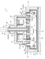
- 진공배기 가능하게 이루어진 처리용기내에서 피처리체에 대하여 소정의 처리를 실시하는 처리 장치에 있어서,상기 처리 장치를 구성함과 동시에 상기 처리용기내의 처리 분위기에 노출되는 구성 부재를 가지고,이 구성 부재의 표면에 자기조직화 단분자막(SAM)으로 이루어지는 막부착 방지층이 형성되어 있는 것을 특징으로 하는처리 장치.
- 제 1 항에 있어서,상기 구성 부재는 적어도 그 표면이 석영으로 구성되고, 이 석영의 표면에 상기 막부착 방지층이 직접 형성되어 있는 것을 특징으로 하는처리 장치.
- 제 2 항에 있어서,상기 구성 부재의 전체가 석영으로 구성되어 있는 것을 특징으로 하는처리 장치.
- 제 1 항에 있어서,상기 구성 부재는 석영이외의 재료로 구성되는 본체 부분과, 상기 본체부분의 표면을 덮는 석영제의 보호 커버를 가지고, 상기 보호 커버의 표면에 상기 막부착 방지층이 형성되어 있는 것을 특징으로 하는처리 장치.
- 제 4 항에 있어서,상기 보호 커버는 상기 본체 부분에 대하여 장착 및 분리가 가능한 것을 특징으로 하는처리 장치.
- 제 1 항에 있어서,상기 구성 부재는 석영이외의 재료로 구성된 본체 부분과, 상기 본체부분의 표면을 피복하는 코팅층을 가지고, 상기 코팅층의 표면에 상기 막부착 방지층이 형성되어 있는 것을 특징으로 하는처리 장치.
- 제 6 항에 있어서,상기 코팅층은 SiO2막인 것을 특징으로 하는처리 장치.
- 제 1 항에 있어서,상기 구성 부재는 상기 처리 용기인 것을 특징으로 하는처리 장치.
- 제 8 항에 있어서,상기 처리용기는 석영제이며, 상기 막부착 방지층은 석영 상에 직접 형성되어 있는 것을 특징으로 하는처리 장치.
- 제 8 항에 있어서,상기 처리용기는 석영이외의 재료로 이루어지고, 상기 처리용기의 내벽면을 덮는 석영제의 보호 커버의 표면에 상기 막부착 방지층이 형성되어 있는 것을 특징으로 하는처리 장치.
- 제 8 항에 있어서,상기 처리용기는 석영이외의 재료로 이루어지고, 상기 처리용기의 내벽면에 SiO2막이 코팅되어, 상기 SiO2막 상에 상기 막부착 방지층이 형성되어 있는 것을 특징으로 하는처리 장치.
- 제 1 항에 있어서,상기 SAM은, OTS(Octadecyltrichlorosilane), DTS(Docosyltrichlorsilane), 및 APTS(3-aminoproyltriethoxysilane)중 어느 하나에 유래하는 것을 특징으로 하는처리 장치.
- 제 1 항에 있어서,상기 소정의 처리는, 성막 처리 또는 스퍼터 처리인 것을 특징으로 하는처리 장치.
- 제 1 항에 있어서,상기 소정의 처리는, 고유전체막, 절연막, 금속막, 금속질화물막 및 금속산화물막 중 어느 하나를 형성하는 성막 처리인 것을 특징으로 하는처리 장치.
Applications Claiming Priority (2)
| Application Number | Priority Date | Filing Date | Title |
|---|---|---|---|
| JPJP-P-2006-104731 | 2006-04-05 | ||
| JP2006104731A JP2007281150A (ja) | 2006-04-05 | 2006-04-05 | 処理装置 |
Publications (2)
| Publication Number | Publication Date |
|---|---|
| KR20080098687A true KR20080098687A (ko) | 2008-11-11 |
| KR101028605B1 KR101028605B1 (ko) | 2011-04-11 |
Family
ID=38581226
Family Applications (1)
| Application Number | Title | Priority Date | Filing Date |
|---|---|---|---|
| KR1020087024299A Expired - Fee Related KR101028605B1 (ko) | 2006-04-05 | 2007-04-05 | 처리 장치 |
Country Status (5)
| Country | Link |
|---|---|
| US (1) | US20090277389A1 (ko) |
| JP (1) | JP2007281150A (ko) |
| KR (1) | KR101028605B1 (ko) |
| CN (1) | CN101356630A (ko) |
| WO (1) | WO2007116940A1 (ko) |
Cited By (6)
| Publication number | Priority date | Publication date | Assignee | Title |
|---|---|---|---|---|
| KR101271499B1 (ko) * | 2011-09-20 | 2013-06-05 | 한국에너지기술연구원 | 반도체 박막 제조용 반응기 및 그를 이용한 반도체 박막 제조 방법 |
| KR20170066081A (ko) * | 2015-12-04 | 2017-06-14 | 삼성전자주식회사 | 수소 플라스마 어닐링 처리 준비 방법, 수소 플라스마 어닐링 처리 방법, 및 수소 플라스마 어닐링 장치 |
| US10508338B2 (en) | 2015-05-26 | 2019-12-17 | The Japan Steel Works, Ltd. | Device for atomic layer deposition |
| US10519549B2 (en) | 2015-05-26 | 2019-12-31 | The Japan Steel Works, Ltd. | Apparatus for plasma atomic layer deposition |
| US10604838B2 (en) | 2015-05-26 | 2020-03-31 | The Japan Steel Works, Ltd. | Apparatus for atomic layer deposition and exhaust unit for apparatus for atomic layer deposition |
| US10633737B2 (en) | 2015-05-26 | 2020-04-28 | The Japan Steel Works, Ltd. | Device for atomic layer deposition |
Families Citing this family (18)
| Publication number | Priority date | Publication date | Assignee | Title |
|---|---|---|---|---|
| CN103014658A (zh) * | 2011-09-28 | 2013-04-03 | 吉富新能源科技(上海)有限公司 | 设计加热平板作升降动作以进行硅薄膜镀膜 |
| JP2014049667A (ja) * | 2012-09-03 | 2014-03-17 | Tokyo Electron Ltd | プラズマ処理装置及びこれを備えた基板処理装置 |
| JP2014154866A (ja) * | 2013-02-14 | 2014-08-25 | Fujifilm Corp | ドライエッチング装置及びドライエッチング装置用のクランプ |
| CN105210173A (zh) * | 2013-05-23 | 2015-12-30 | 应用材料公司 | 用于半导体处理腔室的经涂布的衬里组件 |
| JP6001131B1 (ja) * | 2015-04-28 | 2016-10-05 | 株式会社日立国際電気 | 基板処理装置、半導体装置の製造方法、プログラム |
| JP2017157778A (ja) * | 2016-03-04 | 2017-09-07 | 東京エレクトロン株式会社 | 基板処理装置 |
| CN106222617A (zh) * | 2016-08-26 | 2016-12-14 | 武汉华星光电技术有限公司 | 用于镀膜设备的防着板结构及其制造方法、镀膜设备 |
| JP6309598B2 (ja) * | 2016-11-24 | 2018-04-11 | 株式会社日本製鋼所 | 原子層成長装置 |
| TWI616555B (zh) * | 2017-01-17 | 2018-03-01 | 漢民科技股份有限公司 | 應用於半導體設備之噴氣裝置 |
| WO2019139043A1 (ja) * | 2018-01-10 | 2019-07-18 | Jsr株式会社 | パターン形成方法 |
| US20200075313A1 (en) * | 2018-08-31 | 2020-03-05 | Mattson Technology, Inc. | Oxide Removal From Titanium Nitride Surfaces |
| JP7101628B2 (ja) * | 2019-02-04 | 2022-07-15 | 東京エレクトロン株式会社 | プラズマ処理装置および電極構造体 |
| KR102709799B1 (ko) * | 2019-08-21 | 2024-09-26 | 캐논 톡키 가부시키가이샤 | 밸브 장치 및 성막 장치 |
| KR102404528B1 (ko) | 2019-09-02 | 2022-06-02 | 세메스 주식회사 | 노즐, 이를 포함하는 기판 처리 장치 및 기판 처리 방법 |
| KR102731904B1 (ko) | 2019-12-04 | 2024-11-20 | 주성엔지니어링(주) | 기판 처리 장치, 기판 처리 장치 마련 방법 및 기판 처리 방법 |
| JP2022050198A (ja) * | 2020-09-17 | 2022-03-30 | 東京エレクトロン株式会社 | 成膜方法及び成膜装置 |
| US12606912B2 (en) * | 2020-10-23 | 2026-04-21 | Applied Materials, Inc. | High heat loss heater and electrostatic chuck for semiconductor processing |
| US20250132189A1 (en) * | 2023-10-20 | 2025-04-24 | Applied Materials, Inc. | Lift pins including opening, and related components and chamber kits, for processing chambers |
Family Cites Families (4)
| Publication number | Priority date | Publication date | Assignee | Title |
|---|---|---|---|---|
| JPH11238728A (ja) * | 1997-12-16 | 1999-08-31 | Fujitsu Ltd | 半導体デバイスの製造の際に使用される熱処理治具及びその製造法 |
| JP2000031136A (ja) * | 1998-07-09 | 2000-01-28 | Tokai Carbon Co Ltd | プラズマ処理装置用保護部材 |
| JP4180948B2 (ja) * | 2003-03-24 | 2008-11-12 | 東京エレクトロン株式会社 | 基板処理装置および基板処理方法、ガスノズル |
| EP1623454A2 (en) * | 2003-05-09 | 2006-02-08 | ASM America, Inc. | Reactor surface passivation through chemical deactivation |
-
2006
- 2006-04-05 JP JP2006104731A patent/JP2007281150A/ja active Pending
-
2007
- 2007-04-05 KR KR1020087024299A patent/KR101028605B1/ko not_active Expired - Fee Related
- 2007-04-05 CN CNA2007800012971A patent/CN101356630A/zh active Pending
- 2007-04-05 US US12/296,167 patent/US20090277389A1/en not_active Abandoned
- 2007-04-05 WO PCT/JP2007/057666 patent/WO2007116940A1/ja not_active Ceased
Cited By (6)
| Publication number | Priority date | Publication date | Assignee | Title |
|---|---|---|---|---|
| KR101271499B1 (ko) * | 2011-09-20 | 2013-06-05 | 한국에너지기술연구원 | 반도체 박막 제조용 반응기 및 그를 이용한 반도체 박막 제조 방법 |
| US10508338B2 (en) | 2015-05-26 | 2019-12-17 | The Japan Steel Works, Ltd. | Device for atomic layer deposition |
| US10519549B2 (en) | 2015-05-26 | 2019-12-31 | The Japan Steel Works, Ltd. | Apparatus for plasma atomic layer deposition |
| US10604838B2 (en) | 2015-05-26 | 2020-03-31 | The Japan Steel Works, Ltd. | Apparatus for atomic layer deposition and exhaust unit for apparatus for atomic layer deposition |
| US10633737B2 (en) | 2015-05-26 | 2020-04-28 | The Japan Steel Works, Ltd. | Device for atomic layer deposition |
| KR20170066081A (ko) * | 2015-12-04 | 2017-06-14 | 삼성전자주식회사 | 수소 플라스마 어닐링 처리 준비 방법, 수소 플라스마 어닐링 처리 방법, 및 수소 플라스마 어닐링 장치 |
Also Published As
| Publication number | Publication date |
|---|---|
| US20090277389A1 (en) | 2009-11-12 |
| JP2007281150A (ja) | 2007-10-25 |
| WO2007116940A1 (ja) | 2007-10-18 |
| KR101028605B1 (ko) | 2011-04-11 |
| CN101356630A (zh) | 2009-01-28 |
Similar Documents
| Publication | Publication Date | Title |
|---|---|---|
| KR101028605B1 (ko) | 처리 장치 | |
| CN100474517C (zh) | Ti膜及TiN膜的成膜方法 | |
| KR101804003B1 (ko) | 성막 방법 | |
| US11127597B2 (en) | Etching method | |
| TWI447791B (zh) | 氮化鋁或氧化鈹的陶瓷覆蓋晶圓 | |
| US20190148144A1 (en) | Enhanced selective deposition process | |
| TW201131773A (en) | Semiconductor device, method of manufacturing semiconductor device, and substrate processing apparatus | |
| JP5046506B2 (ja) | 基板処理装置,基板処理方法,プログラム,プログラムを記録した記録媒体 | |
| WO2004021425A1 (ja) | エッチング方法及びエッチング装置 | |
| US20200370174A1 (en) | Substrate support cover for high-temperature corrosive environment | |
| KR100989028B1 (ko) | 반도체 장치의 제조 방법 및 기판 처리 장치 | |
| JP2002035572A (ja) | 真空処理装置と多室型真空処理装置 | |
| KR102023434B1 (ko) | 성막 방법 및 성막 시스템, 그리고 표면 처리 방법 | |
| WO2005054543A1 (ja) | クリーニング方法 | |
| EP1454879A1 (en) | Process for producing thin oxide film and production apparatus | |
| JP4260590B2 (ja) | 基板処理装置のクリーニング方法 | |
| KR20010107744A (ko) | 에칭방법, 처리장치 및 에칭장치 | |
| KR20030083730A (ko) | 기판 처리 장치의 클리닝 방법 및 기판 처리 장치 | |
| TW200416841A (en) | Semiconductor processing method and apparatus for processing target substrate | |
| JP2002008991A (ja) | クリーニング方法 | |
| JP2017212320A (ja) | 酸化チタン膜の形成方法および形成システム、ならびにコンタクト構造の形成方法 | |
| JP5568342B2 (ja) | 半導体装置の製造方法、基板処理方法および基板処理システム | |
| KR102876047B1 (ko) | 성막 방법, 반도체 장치의 제조 방법, 처리 시스템 및 커패시터 | |
| JP2010212391A (ja) | 半導体装置の製造方法及び基板処理装置 | |
| JP4529261B2 (ja) | 複合金属酸化物膜の除去方法、クリーニング方法及びエッチング方法 |
Legal Events
| Date | Code | Title | Description |
|---|---|---|---|
| A201 | Request for examination | ||
| PA0105 | International application |
St.27 status event code: A-0-1-A10-A15-nap-PA0105 |
|
| PA0201 | Request for examination |
St.27 status event code: A-1-2-D10-D11-exm-PA0201 |
|
| PG1501 | Laying open of application |
St.27 status event code: A-1-1-Q10-Q12-nap-PG1501 |
|
| E902 | Notification of reason for refusal | ||
| PE0902 | Notice of grounds for rejection |
St.27 status event code: A-1-2-D10-D21-exm-PE0902 |
|
| E13-X000 | Pre-grant limitation requested |
St.27 status event code: A-2-3-E10-E13-lim-X000 |
|
| P11-X000 | Amendment of application requested |
St.27 status event code: A-2-2-P10-P11-nap-X000 |
|
| P13-X000 | Application amended |
St.27 status event code: A-2-2-P10-P13-nap-X000 |
|
| E701 | Decision to grant or registration of patent right | ||
| PE0701 | Decision of registration |
St.27 status event code: A-1-2-D10-D22-exm-PE0701 |
|
| R17-X000 | Change to representative recorded |
St.27 status event code: A-3-3-R10-R17-oth-X000 |
|
| GRNT | Written decision to grant | ||
| PR0701 | Registration of establishment |
St.27 status event code: A-2-4-F10-F11-exm-PR0701 |
|
| PR1002 | Payment of registration fee |
St.27 status event code: A-2-2-U10-U12-oth-PR1002 Fee payment year number: 1 |
|
| PG1601 | Publication of registration |
St.27 status event code: A-4-4-Q10-Q13-nap-PG1601 |
|
| LAPS | Lapse due to unpaid annual fee | ||
| PC1903 | Unpaid annual fee |
St.27 status event code: A-4-4-U10-U13-oth-PC1903 Not in force date: 20140405 Payment event data comment text: Termination Category : DEFAULT_OF_REGISTRATION_FEE |
|
| PC1903 | Unpaid annual fee |
St.27 status event code: N-4-6-H10-H13-oth-PC1903 Ip right cessation event data comment text: Termination Category : DEFAULT_OF_REGISTRATION_FEE Not in force date: 20140405 |
|
| P22-X000 | Classification modified |
St.27 status event code: A-4-4-P10-P22-nap-X000 |