KR100894306B1 - Organic electroluminescent device - Google Patents
Organic electroluminescent device Download PDFInfo
- Publication number
- KR100894306B1 KR100894306B1 KR1020040082844A KR20040082844A KR100894306B1 KR 100894306 B1 KR100894306 B1 KR 100894306B1 KR 1020040082844 A KR1020040082844 A KR 1020040082844A KR 20040082844 A KR20040082844 A KR 20040082844A KR 100894306 B1 KR100894306 B1 KR 100894306B1
- Authority
- KR
- South Korea
- Prior art keywords
- layer
- organic
- light emitting
- electrode layer
- hole injection
- Prior art date
Links
- 238000002347 injection Methods 0.000 claims abstract description 120
- 239000007924 injection Substances 0.000 claims abstract description 120
- 150000002894 organic compounds Chemical class 0.000 claims abstract description 47
- 229910044991 metal oxide Inorganic materials 0.000 claims abstract description 34
- 150000004706 metal oxides Chemical class 0.000 claims abstract description 33
- 238000006479 redox reaction Methods 0.000 claims abstract description 8
- 239000010410 layer Substances 0.000 claims description 424
- -1 porphyrin compound Chemical class 0.000 claims description 38
- 238000000151 deposition Methods 0.000 claims description 31
- 238000000034 method Methods 0.000 claims description 30
- 239000000758 substrate Substances 0.000 claims description 26
- 238000004544 sputter deposition Methods 0.000 claims description 17
- 230000008021 deposition Effects 0.000 claims description 16
- 239000012044 organic layer Substances 0.000 claims description 11
- 238000012546 transfer Methods 0.000 claims description 11
- 150000005839 radical cations Chemical class 0.000 claims description 8
- 230000008569 process Effects 0.000 claims description 7
- 230000005684 electric field Effects 0.000 claims description 6
- 150000005838 radical anions Chemical class 0.000 claims description 4
- 238000010438 heat treatment Methods 0.000 claims description 3
- 239000000872 buffer Substances 0.000 claims description 2
- 238000000313 electron-beam-induced deposition Methods 0.000 claims 1
- IEQIEDJGQAUEQZ-UHFFFAOYSA-N phthalocyanine Chemical class N1C(N=C2C3=CC=CC=C3C(N=C3C4=CC=CC=C4C(=N4)N3)=N2)=C(C=CC=C2)C2=C1N=C1C2=CC=CC=C2C4=N1 IEQIEDJGQAUEQZ-UHFFFAOYSA-N 0.000 claims 1
- 229910052751 metal Inorganic materials 0.000 description 39
- 239000002184 metal Substances 0.000 description 39
- BAWFJGJZGIEFAR-XUWLLVQESA-N [[(2r,3s,4r,5s)-5-(6-aminopurin-9-yl)-3,4-dihydroxyoxolan-2-yl]methoxy-hydroxyphosphoryl] [(2r,3s,4r,5s)-5-(3-carbamoylpyridin-1-ium-1-yl)-3,4-dihydroxyoxolan-2-yl]methyl phosphate Chemical compound NC(=O)C1=CC=C[N+]([C@@H]2[C@@H]([C@H](O)[C@@H](COP([O-])(=O)OP(O)(=O)OC[C@@H]3[C@H]([C@@H](O)[C@H](O3)N3C4=NC=NC(N)=C4N=C3)O)O2)O)=C1 BAWFJGJZGIEFAR-XUWLLVQESA-N 0.000 description 25
- 230000005525 hole transport Effects 0.000 description 22
- 229910052782 aluminium Inorganic materials 0.000 description 19
- XAGFODPZIPBFFR-UHFFFAOYSA-N aluminium Chemical compound [Al] XAGFODPZIPBFFR-UHFFFAOYSA-N 0.000 description 17
- 230000015572 biosynthetic process Effects 0.000 description 16
- 239000011521 glass Substances 0.000 description 16
- 150000001875 compounds Chemical class 0.000 description 15
- 238000000295 emission spectrum Methods 0.000 description 15
- 238000000862 absorption spectrum Methods 0.000 description 11
- 230000004888 barrier function Effects 0.000 description 11
- 238000012360 testing method Methods 0.000 description 10
- 239000007772 electrode material Substances 0.000 description 9
- 150000002739 metals Chemical class 0.000 description 9
- 238000003475 lamination Methods 0.000 description 8
- 238000006722 reduction reaction Methods 0.000 description 8
- 239000000523 sample Substances 0.000 description 8
- 239000002841 Lewis acid Substances 0.000 description 7
- 239000011777 magnesium Substances 0.000 description 7
- 238000004519 manufacturing process Methods 0.000 description 7
- 230000009467 reduction Effects 0.000 description 7
- AMGQUBHHOARCQH-UHFFFAOYSA-N indium;oxotin Chemical compound [In].[Sn]=O AMGQUBHHOARCQH-UHFFFAOYSA-N 0.000 description 6
- 229910052749 magnesium Inorganic materials 0.000 description 6
- 229910052709 silver Inorganic materials 0.000 description 6
- WHXSMMKQMYFTQS-UHFFFAOYSA-N Lithium Chemical compound [Li] WHXSMMKQMYFTQS-UHFFFAOYSA-N 0.000 description 5
- FYYHWMGAXLPEAU-UHFFFAOYSA-N Magnesium Chemical compound [Mg] FYYHWMGAXLPEAU-UHFFFAOYSA-N 0.000 description 5
- 238000011156 evaluation Methods 0.000 description 5
- 229910052744 lithium Inorganic materials 0.000 description 5
- BQCADISMDOOEFD-UHFFFAOYSA-N Silver Chemical compound [Ag] BQCADISMDOOEFD-UHFFFAOYSA-N 0.000 description 4
- 229910052783 alkali metal Inorganic materials 0.000 description 4
- 150000001340 alkali metals Chemical class 0.000 description 4
- 229910045601 alloy Inorganic materials 0.000 description 4
- 239000000956 alloy Substances 0.000 description 4
- 238000011161 development Methods 0.000 description 4
- ZUOUZKKEUPVFJK-UHFFFAOYSA-N diphenyl Chemical compound C1=CC=CC=C1C1=CC=CC=C1 ZUOUZKKEUPVFJK-UHFFFAOYSA-N 0.000 description 4
- 230000000694 effects Effects 0.000 description 4
- 239000005357 flat glass Substances 0.000 description 4
- IBHBKWKFFTZAHE-UHFFFAOYSA-N n-[4-[4-(n-naphthalen-1-ylanilino)phenyl]phenyl]-n-phenylnaphthalen-1-amine Chemical compound C1=CC=CC=C1N(C=1C2=CC=CC=C2C=CC=1)C1=CC=C(C=2C=CC(=CC=2)N(C=2C=CC=CC=2)C=2C3=CC=CC=C3C=CC=2)C=C1 IBHBKWKFFTZAHE-UHFFFAOYSA-N 0.000 description 4
- 230000003287 optical effect Effects 0.000 description 4
- 238000011160 research Methods 0.000 description 4
- 239000004332 silver Substances 0.000 description 4
- 229910001413 alkali metal ion Inorganic materials 0.000 description 3
- XCJYREBRNVKWGJ-UHFFFAOYSA-N copper(II) phthalocyanine Chemical compound [Cu+2].C12=CC=CC=C2C(N=C2[N-]C(C3=CC=CC=C32)=N2)=NC1=NC([C]1C=CC=CC1=1)=NC=1N=C1[C]3C=CC=CC3=C2[N-]1 XCJYREBRNVKWGJ-UHFFFAOYSA-N 0.000 description 3
- 230000005284 excitation Effects 0.000 description 3
- 229910021645 metal ion Inorganic materials 0.000 description 3
- 239000002245 particle Substances 0.000 description 3
- 125000002924 primary amino group Chemical group [H]N([H])* 0.000 description 3
- 229910052761 rare earth metal Inorganic materials 0.000 description 3
- 238000001228 spectrum Methods 0.000 description 3
- 238000001771 vacuum deposition Methods 0.000 description 3
- 125000001637 1-naphthyl group Chemical group [H]C1=C([H])C([H])=C2C(*)=C([H])C([H])=C([H])C2=C1[H] 0.000 description 2
- MQRCTQVBZYBPQE-UHFFFAOYSA-N 189363-47-1 Chemical compound C1=CC=CC=C1N(C=1C=C2C3(C4=CC(=CC=C4C2=CC=1)N(C=1C=CC=CC=1)C=1C=CC=CC=1)C1=CC(=CC=C1C1=CC=C(C=C13)N(C=1C=CC=CC=1)C=1C=CC=CC=1)N(C=1C=CC=CC=1)C=1C=CC=CC=1)C1=CC=CC=C1 MQRCTQVBZYBPQE-UHFFFAOYSA-N 0.000 description 2
- 241000284156 Clerodendrum quadriloculare Species 0.000 description 2
- UFWIBTONFRDIAS-UHFFFAOYSA-N Naphthalene Chemical compound C1=CC=CC2=CC=CC=C21 UFWIBTONFRDIAS-UHFFFAOYSA-N 0.000 description 2
- 229910001420 alkaline earth metal ion Inorganic materials 0.000 description 2
- 150000004982 aromatic amines Chemical class 0.000 description 2
- 235000010290 biphenyl Nutrition 0.000 description 2
- 239000004305 biphenyl Substances 0.000 description 2
- 238000010586 diagram Methods 0.000 description 2
- 239000010408 film Substances 0.000 description 2
- 230000009477 glass transition Effects 0.000 description 2
- 239000000463 material Substances 0.000 description 2
- 238000005259 measurement Methods 0.000 description 2
- 238000000691 measurement method Methods 0.000 description 2
- 239000000203 mixture Substances 0.000 description 2
- UHVLDCDWBKWDDN-UHFFFAOYSA-N n-phenyl-n-[4-[4-(n-pyren-2-ylanilino)phenyl]phenyl]pyren-2-amine Chemical group C1=CC=CC=C1N(C=1C=C2C=CC3=CC=CC4=CC=C(C2=C43)C=1)C1=CC=C(C=2C=CC(=CC=2)N(C=2C=CC=CC=2)C=2C=C3C=CC4=CC=CC5=CC=C(C3=C54)C=2)C=C1 UHVLDCDWBKWDDN-UHFFFAOYSA-N 0.000 description 2
- 239000011368 organic material Substances 0.000 description 2
- 125000002524 organometallic group Chemical group 0.000 description 2
- 229910052718 tin Inorganic materials 0.000 description 2
- 229910052720 vanadium Inorganic materials 0.000 description 2
- LEONUFNNVUYDNQ-UHFFFAOYSA-N vanadium atom Chemical compound [V] LEONUFNNVUYDNQ-UHFFFAOYSA-N 0.000 description 2
- YJTKZCDBKVTVBY-UHFFFAOYSA-N 1,3-Diphenylbenzene Chemical group C1=CC=CC=C1C1=CC=CC(C=2C=CC=CC=2)=C1 YJTKZCDBKVTVBY-UHFFFAOYSA-N 0.000 description 1
- XJKSTNDFUHDPQJ-UHFFFAOYSA-N 1,4-diphenylbenzene Chemical group C1=CC=CC=C1C1=CC=C(C=2C=CC=CC=2)C=C1 XJKSTNDFUHDPQJ-UHFFFAOYSA-N 0.000 description 1
- LQRAULANJCQXAM-UHFFFAOYSA-N 1-n,5-n-dinaphthalen-1-yl-1-n,5-n-diphenylnaphthalene-1,5-diamine Chemical compound C1=CC=CC=C1N(C=1C2=CC=CC(=C2C=CC=1)N(C=1C=CC=CC=1)C=1C2=CC=CC=C2C=CC=1)C1=CC=CC2=CC=CC=C12 LQRAULANJCQXAM-UHFFFAOYSA-N 0.000 description 1
- ZDAWFMCVTXSZTC-UHFFFAOYSA-N 2-n',7-n'-dinaphthalen-1-yl-2-n',7-n'-diphenyl-9,9'-spirobi[fluorene]-2',7'-diamine Chemical compound C1=CC=CC=C1N(C=1C2=CC=CC=C2C=CC=1)C1=CC=C(C=2C(=CC(=CC=2)N(C=2C=CC=CC=2)C=2C3=CC=CC=C3C=CC=2)C23C4=CC=CC=C4C4=CC=CC=C43)C2=C1 ZDAWFMCVTXSZTC-UHFFFAOYSA-N 0.000 description 1
- DJIXFCSAUCLVLK-UHFFFAOYSA-N 2-n,2-n,6-n,6-n-tetranaphthalen-2-yl-9h-fluorene-2,6-diamine Chemical compound C1=CC=CC2=CC(N(C=3C=C4C=CC=CC4=CC=3)C3=CC=C4CC5=CC(=CC=C5C4=C3)N(C=3C=C4C=CC=CC4=CC=3)C=3C=C4C=CC=CC4=CC=3)=CC=C21 DJIXFCSAUCLVLK-UHFFFAOYSA-N 0.000 description 1
- 125000001622 2-naphthyl group Chemical group [H]C1=C([H])C([H])=C2C([H])=C(*)C([H])=C([H])C2=C1[H] 0.000 description 1
- OGGKVJMNFFSDEV-UHFFFAOYSA-N 3-methyl-n-[4-[4-(n-(3-methylphenyl)anilino)phenyl]phenyl]-n-phenylaniline Chemical group CC1=CC=CC(N(C=2C=CC=CC=2)C=2C=CC(=CC=2)C=2C=CC(=CC=2)N(C=2C=CC=CC=2)C=2C=C(C)C=CC=2)=C1 OGGKVJMNFFSDEV-UHFFFAOYSA-N 0.000 description 1
- AHDTYXOIJHCGKH-UHFFFAOYSA-N 4-[[4-(dimethylamino)-2-methylphenyl]-phenylmethyl]-n,n,3-trimethylaniline Chemical compound CC1=CC(N(C)C)=CC=C1C(C=1C(=CC(=CC=1)N(C)C)C)C1=CC=CC=C1 AHDTYXOIJHCGKH-UHFFFAOYSA-N 0.000 description 1
- DUSWRTUHJVJVRY-UHFFFAOYSA-N 4-methyl-n-[4-[2-[4-(4-methyl-n-(4-methylphenyl)anilino)phenyl]propan-2-yl]phenyl]-n-(4-methylphenyl)aniline Chemical compound C1=CC(C)=CC=C1N(C=1C=CC(=CC=1)C(C)(C)C=1C=CC(=CC=1)N(C=1C=CC(C)=CC=1)C=1C=CC(C)=CC=1)C1=CC=C(C)C=C1 DUSWRTUHJVJVRY-UHFFFAOYSA-N 0.000 description 1
- MVIXNQZIMMIGEL-UHFFFAOYSA-N 4-methyl-n-[4-[4-(4-methyl-n-(4-methylphenyl)anilino)phenyl]phenyl]-n-(4-methylphenyl)aniline Chemical group C1=CC(C)=CC=C1N(C=1C=CC(=CC=1)C=1C=CC(=CC=1)N(C=1C=CC(C)=CC=1)C=1C=CC(C)=CC=1)C1=CC=C(C)C=C1 MVIXNQZIMMIGEL-UHFFFAOYSA-N 0.000 description 1
- XIQGFRHAIQHZBD-UHFFFAOYSA-N 4-methyl-n-[4-[[4-(4-methyl-n-(4-methylphenyl)anilino)phenyl]-phenylmethyl]phenyl]-n-(4-methylphenyl)aniline Chemical compound C1=CC(C)=CC=C1N(C=1C=CC(=CC=1)C(C=1C=CC=CC=1)C=1C=CC(=CC=1)N(C=1C=CC(C)=CC=1)C=1C=CC(C)=CC=1)C1=CC=C(C)C=C1 XIQGFRHAIQHZBD-UHFFFAOYSA-N 0.000 description 1
- VIJYEGDOKCKUOL-UHFFFAOYSA-N 9-phenylcarbazole Chemical compound C1=CC=CC=C1N1C2=CC=CC=C2C2=CC=CC=C21 VIJYEGDOKCKUOL-UHFFFAOYSA-N 0.000 description 1
- 229910000861 Mg alloy Inorganic materials 0.000 description 1
- 229910003023 Mg-Al Inorganic materials 0.000 description 1
- DWHUCVHMSFNQFI-UHFFFAOYSA-N N-[4-[4-(N-coronen-1-ylanilino)phenyl]phenyl]-N-phenylcoronen-1-amine Chemical group C1=CC=CC=C1N(C=1C2=CC=C3C=CC4=CC=C5C=CC6=CC=C(C7=C6C5=C4C3=C72)C=1)C1=CC=C(C=2C=CC(=CC=2)N(C=2C=CC=CC=2)C=2C3=CC=C4C=CC5=CC=C6C=CC7=CC=C(C8=C7C6=C5C4=C83)C=2)C=C1 DWHUCVHMSFNQFI-UHFFFAOYSA-N 0.000 description 1
- 229910052772 Samarium Inorganic materials 0.000 description 1
- PJANXHGTPQOBST-VAWYXSNFSA-N Stilbene Natural products C=1C=CC=CC=1/C=C/C1=CC=CC=C1 PJANXHGTPQOBST-VAWYXSNFSA-N 0.000 description 1
- 239000007983 Tris buffer Substances 0.000 description 1
- QCWXUUIWCKQGHC-UHFFFAOYSA-N Zirconium Chemical compound [Zr] QCWXUUIWCKQGHC-UHFFFAOYSA-N 0.000 description 1
- XHCLAFWTIXFWPH-UHFFFAOYSA-N [O-2].[O-2].[O-2].[O-2].[O-2].[V+5].[V+5] Chemical compound [O-2].[O-2].[O-2].[O-2].[O-2].[V+5].[V+5] XHCLAFWTIXFWPH-UHFFFAOYSA-N 0.000 description 1
- 238000010521 absorption reaction Methods 0.000 description 1
- 239000002253 acid Substances 0.000 description 1
- 229910052784 alkaline earth metal Inorganic materials 0.000 description 1
- 150000001342 alkaline earth metals Chemical class 0.000 description 1
- 150000001412 amines Chemical class 0.000 description 1
- 125000002029 aromatic hydrocarbon group Chemical group 0.000 description 1
- 229910052792 caesium Inorganic materials 0.000 description 1
- TVFDJXOCXUVLDH-UHFFFAOYSA-N caesium atom Chemical compound [Cs] TVFDJXOCXUVLDH-UHFFFAOYSA-N 0.000 description 1
- 239000010406 cathode material Substances 0.000 description 1
- 238000006243 chemical reaction Methods 0.000 description 1
- 238000010276 construction Methods 0.000 description 1
- 238000007796 conventional method Methods 0.000 description 1
- 239000013078 crystal Substances 0.000 description 1
- 238000005137 deposition process Methods 0.000 description 1
- 238000013461 design Methods 0.000 description 1
- 238000005401 electroluminescence Methods 0.000 description 1
- 238000005516 engineering process Methods 0.000 description 1
- 230000001747 exhibiting effect Effects 0.000 description 1
- RBTKNAXYKSUFRK-UHFFFAOYSA-N heliogen blue Chemical compound [Cu].[N-]1C2=C(C=CC=C3)C3=C1N=C([N-]1)C3=CC=CC=C3C1=NC([N-]1)=C(C=CC=C3)C3=C1N=C([N-]1)C3=CC=CC=C3C1=N2 RBTKNAXYKSUFRK-UHFFFAOYSA-N 0.000 description 1
- 238000011065 in-situ storage Methods 0.000 description 1
- 229910052738 indium Inorganic materials 0.000 description 1
- 150000002484 inorganic compounds Chemical class 0.000 description 1
- 229910010272 inorganic material Inorganic materials 0.000 description 1
- 239000011810 insulating material Substances 0.000 description 1
- 229910052745 lead Inorganic materials 0.000 description 1
- 150000007517 lewis acids Chemical class 0.000 description 1
- 239000004973 liquid crystal related substance Substances 0.000 description 1
- FUJCRWPEOMXPAD-UHFFFAOYSA-N lithium oxide Chemical compound [Li+].[Li+].[O-2] FUJCRWPEOMXPAD-UHFFFAOYSA-N 0.000 description 1
- 229910001947 lithium oxide Inorganic materials 0.000 description 1
- 229910052748 manganese Inorganic materials 0.000 description 1
- 229910000476 molybdenum oxide Inorganic materials 0.000 description 1
- BBDFECYVDQCSCN-UHFFFAOYSA-N n-(4-methoxyphenyl)-4-[4-(n-(4-methoxyphenyl)anilino)phenyl]-n-phenylaniline Chemical group C1=CC(OC)=CC=C1N(C=1C=CC(=CC=1)C=1C=CC(=CC=1)N(C=1C=CC=CC=1)C=1C=CC(OC)=CC=1)C1=CC=CC=C1 BBDFECYVDQCSCN-UHFFFAOYSA-N 0.000 description 1
- RBFKMWWGVFIFIP-UHFFFAOYSA-N n-(4-naphthalen-1-ylphenyl)-n,2-diphenylaniline Chemical group C1=CC=CC=C1N(C=1C(=CC=CC=1)C=1C=CC=CC=1)C1=CC=C(C=2C3=CC=CC=C3C=CC=2)C=C1 RBFKMWWGVFIFIP-UHFFFAOYSA-N 0.000 description 1
- OMQCLPPEEURTMR-UHFFFAOYSA-N n-[4-[4-(n-fluoranthen-8-ylanilino)phenyl]phenyl]-n-phenylfluoranthen-8-amine Chemical group C1=CC=CC=C1N(C=1C=C2C(C=3C=CC=C4C=CC=C2C=34)=CC=1)C1=CC=C(C=2C=CC(=CC=2)N(C=2C=CC=CC=2)C=2C=C3C(C=4C=CC=C5C=CC=C3C=45)=CC=2)C=C1 OMQCLPPEEURTMR-UHFFFAOYSA-N 0.000 description 1
- BLFVVZKSHYCRDR-UHFFFAOYSA-N n-[4-[4-(n-naphthalen-2-ylanilino)phenyl]phenyl]-n-phenylnaphthalen-2-amine Chemical group C1=CC=CC=C1N(C=1C=C2C=CC=CC2=CC=1)C1=CC=C(C=2C=CC(=CC=2)N(C=2C=CC=CC=2)C=2C=C3C=CC=CC3=CC=2)C=C1 BLFVVZKSHYCRDR-UHFFFAOYSA-N 0.000 description 1
- LUBWJINDFCNHLI-UHFFFAOYSA-N n-[4-[4-(n-perylen-2-ylanilino)phenyl]phenyl]-n-phenylperylen-2-amine Chemical group C1=CC=CC=C1N(C=1C=C2C=3C=CC=C4C=CC=C(C=34)C=3C=CC=C(C2=3)C=1)C1=CC=C(C=2C=CC(=CC=2)N(C=2C=CC=CC=2)C=2C=C3C=4C=CC=C5C=CC=C(C=45)C=4C=CC=C(C3=4)C=2)C=C1 LUBWJINDFCNHLI-UHFFFAOYSA-N 0.000 description 1
- TUPXWIUQIGEYST-UHFFFAOYSA-N n-[4-[4-(n-phenanthren-2-ylanilino)phenyl]phenyl]-n-phenylphenanthren-2-amine Chemical group C1=CC=CC=C1N(C=1C=C2C(C3=CC=CC=C3C=C2)=CC=1)C1=CC=C(C=2C=CC(=CC=2)N(C=2C=CC=CC=2)C=2C=C3C(C4=CC=CC=C4C=C3)=CC=2)C=C1 TUPXWIUQIGEYST-UHFFFAOYSA-N 0.000 description 1
- NBHXGUASDDSHGV-UHFFFAOYSA-N n-[4-[4-[4-(n-naphthalen-1-ylanilino)phenyl]phenyl]phenyl]-n-phenylnaphthalen-1-amine Chemical group C1=CC=CC=C1N(C=1C2=CC=CC=C2C=CC=1)C1=CC=C(C=2C=CC(=CC=2)C=2C=CC(=CC=2)N(C=2C=CC=CC=2)C=2C3=CC=CC=C3C=CC=2)C=C1 NBHXGUASDDSHGV-UHFFFAOYSA-N 0.000 description 1
- RJSTZCQRFUSBJV-UHFFFAOYSA-N n-[4-[4-[n-(1,2-dihydroacenaphthylen-3-yl)anilino]phenyl]phenyl]-n-phenyl-1,2-dihydroacenaphthylen-3-amine Chemical group C1=CC(C2=3)=CC=CC=3CCC2=C1N(C=1C=CC(=CC=1)C=1C=CC(=CC=1)N(C=1C=CC=CC=1)C=1C=2CCC3=CC=CC(C=23)=CC=1)C1=CC=CC=C1 RJSTZCQRFUSBJV-UHFFFAOYSA-N 0.000 description 1
- 239000007800 oxidant agent Substances 0.000 description 1
- 230000001590 oxidative effect Effects 0.000 description 1
- PQQKPALAQIIWST-UHFFFAOYSA-N oxomolybdenum Chemical compound [Mo]=O PQQKPALAQIIWST-UHFFFAOYSA-N 0.000 description 1
- 229930184652 p-Terphenyl Natural products 0.000 description 1
- GPRIERYVMZVKTC-UHFFFAOYSA-N p-quaterphenyl Chemical group C1=CC=CC=C1C1=CC=C(C=2C=CC(=CC=2)C=2C=CC=CC=2)C=C1 GPRIERYVMZVKTC-UHFFFAOYSA-N 0.000 description 1
- 229920000642 polymer Polymers 0.000 description 1
- 238000007639 printing Methods 0.000 description 1
- 150000002910 rare earth metals Chemical class 0.000 description 1
- 230000009257 reactivity Effects 0.000 description 1
- 230000027756 respiratory electron transport chain Effects 0.000 description 1
- KZUNJOHGWZRPMI-UHFFFAOYSA-N samarium atom Chemical compound [Sm] KZUNJOHGWZRPMI-UHFFFAOYSA-N 0.000 description 1
- 230000000087 stabilizing effect Effects 0.000 description 1
- PJANXHGTPQOBST-UHFFFAOYSA-N stilbene Chemical compound C=1C=CC=CC=1C=CC1=CC=CC=C1 PJANXHGTPQOBST-UHFFFAOYSA-N 0.000 description 1
- 235000021286 stilbenes Nutrition 0.000 description 1
- 229910052712 strontium Inorganic materials 0.000 description 1
- CIOAGBVUUVVLOB-UHFFFAOYSA-N strontium atom Chemical compound [Sr] CIOAGBVUUVVLOB-UHFFFAOYSA-N 0.000 description 1
- 125000005504 styryl group Chemical group 0.000 description 1
- 239000000126 substance Substances 0.000 description 1
- 125000001424 substituent group Chemical group 0.000 description 1
- 239000010409 thin film Substances 0.000 description 1
- 238000002834 transmittance Methods 0.000 description 1
- LENZDBCJOHFCAS-UHFFFAOYSA-N tris Chemical compound OCC(N)(CO)CO LENZDBCJOHFCAS-UHFFFAOYSA-N 0.000 description 1
- 238000007738 vacuum evaporation Methods 0.000 description 1
- 229910001935 vanadium oxide Inorganic materials 0.000 description 1
- 229910052726 zirconium Inorganic materials 0.000 description 1
Images


Classifications
-
- H—ELECTRICITY
- H10—SEMICONDUCTOR DEVICES; ELECTRIC SOLID-STATE DEVICES NOT OTHERWISE PROVIDED FOR
- H10K—ORGANIC ELECTRIC SOLID-STATE DEVICES
- H10K50/00—Organic light-emitting devices
- H10K50/10—OLEDs or polymer light-emitting diodes [PLED]
- H10K50/17—Carrier injection layers
-
- C—CHEMISTRY; METALLURGY
- C09—DYES; PAINTS; POLISHES; NATURAL RESINS; ADHESIVES; COMPOSITIONS NOT OTHERWISE PROVIDED FOR; APPLICATIONS OF MATERIALS NOT OTHERWISE PROVIDED FOR
- C09K—MATERIALS FOR MISCELLANEOUS APPLICATIONS, NOT PROVIDED FOR ELSEWHERE
- C09K11/00—Luminescent, e.g. electroluminescent, chemiluminescent materials
- C09K11/06—Luminescent, e.g. electroluminescent, chemiluminescent materials containing organic luminescent materials
-
- H—ELECTRICITY
- H05—ELECTRIC TECHNIQUES NOT OTHERWISE PROVIDED FOR
- H05B—ELECTRIC HEATING; ELECTRIC LIGHT SOURCES NOT OTHERWISE PROVIDED FOR; CIRCUIT ARRANGEMENTS FOR ELECTRIC LIGHT SOURCES, IN GENERAL
- H05B33/00—Electroluminescent light sources
- H05B33/12—Light sources with substantially two-dimensional radiating surfaces
- H05B33/14—Light sources with substantially two-dimensional radiating surfaces characterised by the chemical or physical composition or the arrangement of the electroluminescent material, or by the simultaneous addition of the electroluminescent material in or onto the light source
-
- H—ELECTRICITY
- H10—SEMICONDUCTOR DEVICES; ELECTRIC SOLID-STATE DEVICES NOT OTHERWISE PROVIDED FOR
- H10K—ORGANIC ELECTRIC SOLID-STATE DEVICES
- H10K85/00—Organic materials used in the body or electrodes of devices covered by this subclass
- H10K85/30—Coordination compounds
-
- H—ELECTRICITY
- H10—SEMICONDUCTOR DEVICES; ELECTRIC SOLID-STATE DEVICES NOT OTHERWISE PROVIDED FOR
- H10K—ORGANIC ELECTRIC SOLID-STATE DEVICES
- H10K85/00—Organic materials used in the body or electrodes of devices covered by this subclass
- H10K85/30—Coordination compounds
- H10K85/321—Metal complexes comprising a group IIIA element, e.g. Tris (8-hydroxyquinoline) gallium [Gaq3]
- H10K85/324—Metal complexes comprising a group IIIA element, e.g. Tris (8-hydroxyquinoline) gallium [Gaq3] comprising aluminium, e.g. Alq3
-
- H—ELECTRICITY
- H10—SEMICONDUCTOR DEVICES; ELECTRIC SOLID-STATE DEVICES NOT OTHERWISE PROVIDED FOR
- H10K—ORGANIC ELECTRIC SOLID-STATE DEVICES
- H10K85/00—Organic materials used in the body or electrodes of devices covered by this subclass
- H10K85/60—Organic compounds having low molecular weight
- H10K85/615—Polycyclic condensed aromatic hydrocarbons, e.g. anthracene
-
- H—ELECTRICITY
- H10—SEMICONDUCTOR DEVICES; ELECTRIC SOLID-STATE DEVICES NOT OTHERWISE PROVIDED FOR
- H10K—ORGANIC ELECTRIC SOLID-STATE DEVICES
- H10K85/00—Organic materials used in the body or electrodes of devices covered by this subclass
- H10K85/60—Organic compounds having low molecular weight
- H10K85/631—Amine compounds having at least two aryl rest on at least one amine-nitrogen atom, e.g. triphenylamine
-
- H—ELECTRICITY
- H10—SEMICONDUCTOR DEVICES; ELECTRIC SOLID-STATE DEVICES NOT OTHERWISE PROVIDED FOR
- H10K—ORGANIC ELECTRIC SOLID-STATE DEVICES
- H10K85/00—Organic materials used in the body or electrodes of devices covered by this subclass
- H10K85/60—Organic compounds having low molecular weight
- H10K85/649—Aromatic compounds comprising a hetero atom
Abstract
유기전계발광소자는 양극전극층, 양극전극층에 대향되는 음극전극층, 양극전극층에 접하게 제공된 홀주입층 및 양극전극층과 음극전극층 사이에 적어도 하나의 발광층 또는 적어도 하나의 발광층을 가지는 적어도 하나의 발광유닛을 포함하는 유기구조체를 포함한다. 양극전극층과 음극전극층 중 적어도 하나는 투명하다. 홀주입층은 금속산화물과 유기화합물의 혼합층을 포함한다. 혼합층은 금속산화물과 유기화합물의 공증착으로 형성된다.The organic light emitting device includes an anode electrode layer, a cathode electrode layer facing the anode electrode layer, a hole injection layer provided in contact with the anode electrode layer, and at least one light emitting unit having at least one emitting layer or at least one emitting layer between the anode electrode layer and the cathode electrode layer. It includes an organic structure. At least one of the anode electrode layer and the cathode electrode layer is transparent. The hole injection layer includes a mixed layer of a metal oxide and an organic compound. The mixed layer is formed by co-deposition of metal oxides and organic compounds.
홀주입층, 금속산화물, 유기화합물, 혼합층, 공증착, 산화환원반응, 일함수Hole injection layer, metal oxide, organic compound, mixed layer, co-deposition, redox reaction, work function
Description
도 1은 전하인가시 전하이동착체의 형성 및 홀의 이동을 설명하는 홀주입층의 개략도이다.1 is a schematic diagram of a hole injection layer illustrating the formation of charge transfer complexes and the movement of holes upon charge application.
도 2는 아릴아민화합물인 2-TNATA, α-NPD, 스피로(spiro)-TAD 또는 스피로(spiro)-NPB 또는 금속산화물인 V2O5(바나디움펜토사이드)를 단독으로 사용해 얻어지는 흡수스펙트럼과 각 아릴아민화합물과 바나디움펜토사이드의 혼합층의 흡수스펙트럼이다.2 is an absorption spectrum obtained by using an arylamine compound, 2-TNATA, α-NPD, spiro-TAD or spiro-NPB, or a metal oxide, V 2 O 5 (vanadium pentoside) alone, and Absorption spectrum of the mixed layer of an arylamine compound and vanadium pentoside.
도 3은 α-NPD 및 Re2O7(디레니움헵토사이드)의 혼합층으로 얻어지는 흡수스펙트럼이다.FIG. 3 is an absorption spectrum obtained with a mixed layer of α-NPD and Re 2 O 7 (dreniumheptoside). FIG.
도 4는 기준예에 따른 유기EL소자의 적층구조를 보여주는 개략도이다.4 is a schematic diagram showing a laminated structure of an organic EL element according to a reference example.
도 5는 실시예1에 따른 유기EL소자의 적층구조를 보여주는 개략도이다.5 is a schematic view showing the laminated structure of the organic EL device according to the first embodiment.
도 6은 실시예2에 따른 유기EL소자의 적층구조를 보여주는 개략도이다.6 is a schematic view showing the lamination structure of the organic EL device according to the second embodiment.
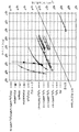
도 7은 기준예, 실시예1 및 2에 따른 유기EL소자의 구동전압(V)에 대한 전류밀도(㎃/㎠)의 특성곡선을 보여주는 그래프이다.7 is a graph showing characteristic curves of current density (kW / cm 2) with respect to the driving voltage V of the organic EL device according to the reference example, Examples 1 and 2;
도 8은 기준예, 실시예1 및 2에 따른 유기EL소자의 구동전압(V)에 대한 휘도(cd/㎡)의 특성곡선을 보여주는 그래프이다. FIG. 8 is a graph showing a characteristic curve of luminance (cd / m 2) with respect to the driving voltage V of the organic EL device according to the reference example, Examples 1 and 2. FIG.
도 9는 기준예, 실시예1 및 2에 따른 유기EL소자의 전류밀도(㎃/㎠)에 대한 전류효율(cd/A)의 특성곡선을 보여주는 그래프이다.9 is a graph showing characteristic curves of current efficiency (cd / A) versus current density (밀도 / cm 2) of organic EL devices according to Reference Examples, Examples 1 and 2;
도 10은 기준예, 실시예1 및 2에 따른 유기EL소자의 휘도(cd/㎡)에 대한 전력효율(1m/W)의 특성곡선을 보여주는 그래프이다.FIG. 10 is a graph showing characteristic curves of power efficiency (1 m / W) with respect to luminance (cd / m 2) of organic EL devices according to Reference Examples, Examples 1 and 2. FIG.
도 11은 기준예, 실시예1 및 2에 따른 유기EL소자의 발광스펙트럼을 보여주는 그래프이다.FIG. 11 is a graph showing emission spectra of organic EL devices according to Reference Examples and Examples 1 and 2. FIG.
도 12는 실시예3에 따른 유기EL소자의 적층구조를 보여주는 개략도이다. 12 is a schematic view showing the laminated structure of the organic EL device according to the third embodiment.
도 13은 실시예3에 따른 유기EL소자의 구동전압(V)에 대한 전류밀도(㎃/㎠)의 특성곡선을 보여주는 그래프이다.FIG. 13 is a graph showing a characteristic curve of current density (kW / cm 2) with respect to the driving voltage V of the organic EL device according to Example 3. FIG.
도 14는 실시예3에 따른 유기EL소자의 구동전압(V)에 대한 휘도(cd/㎡)의 특성곡선을 보여주는 그래프이다. 14 is a graph showing a characteristic curve of luminance (cd / m 2) with respect to the driving voltage V of the organic EL device according to the third embodiment.
도 15는 실시예3에 따른 유기EL소자의 전류밀도(㎃/㎠)에 대한 전류효율(cd/A)의 특성곡선을 보여주는 그래프이다.FIG. 15 is a graph showing a characteristic curve of current efficiency (cd / A) versus current density (㎃ / cm 2) of the organic EL device according to Example 3. FIG.
도 16은 실시예3에 따른 유기EL소자의 휘도(cd/㎡)에 대한 전력효율(1m/W)의 특성곡선을 보여주는 그래프이다.16 is a graph showing a characteristic curve of power efficiency (1 m / W) with respect to luminance (cd / m 2) of the organic EL device according to Example 3. FIG.
도 17은 실시예3에 따른 유기EL소자의 발광스펙트럼을 보여주는 그래프이다.17 is a graph showing the emission spectrum of the organic EL device according to the third embodiment.
도 18은 실시예4에 따른 유기EL소자의 적층구조를 보여주는 개략도이다.18 is a schematic view showing the laminated structure of the organic EL device according to the fourth embodiment.
도 19는 실시예4에 따른 유기EL소자의 구동전압(V)에 대한 전류밀도(㎃/㎠)의 특성곡선을 보여주는 그래프이다.19 is a graph showing a characteristic curve of current density (kW / cm 2) with respect to the driving voltage V of the organic EL device according to the fourth embodiment.
도 20은 실시예4에 따른 유기EL소자의 구동전압(V)에 대한 휘도(cd/㎡)의 특 성곡선을 보여주는 그래프이다. 20 is a graph showing a characteristic curve of luminance (cd / m 2) with respect to the driving voltage V of the organic EL device according to the fourth embodiment.
도 21은 실시예4에 따른 유기EL소자의 전류밀도(㎃/㎠)에 대한 전류효율(cd/A)의 특성곡선을 보여주는 그래프이다.FIG. 21 is a graph showing a characteristic curve of current efficiency (cd / A) versus current density (밀도 / cm 2) of the organic EL device according to Example 4. FIG.
도 22는 실시예4에 따른 유기EL소자의 휘도(cd/㎡)에 대한 전력효율(1m/W)의 특성곡선을 보여주는 그래프이다. 22 is a graph showing a characteristic curve of power efficiency (1 m / W) with respect to luminance (cd / m 2) of the organic EL device according to Example 4. FIG.
도 23은 실시예4에 따른 유기EL소자의 발광스펙트럼을 보여주는 그래프이다.Fig. 23 is a graph showing the emission spectrum of the organic EL device according to the fourth embodiment.
도 24는 실시예5에 따른 유기EL소자의 적층구조를 부요주는 개략도이다.Fig. 24 is a schematic view that gives the laminated structure of the organic EL element according to the fifth embodiment.
도 25는 실시예5에 따른 유기EL소자의 구동전압(V)에 대한 전류밀도(㎃/㎠)의 특성곡선을 보여주는 그래프이다.FIG. 25 is a graph showing a characteristic curve of current density (kW / cm 2) with respect to the driving voltage V of the organic EL device according to Example 5. FIG.
도 26은 실시예5에 따른 유기EL소자의 구동전압(V)에 대한 휘도(cd/㎡)의 특성곡선을 보여주는 그래프이다.FIG. 26 is a graph showing a characteristic curve of luminance (cd / m 2) with respect to the driving voltage V of the organic EL element according to Example 5. FIG.
도 27은 실시예5에 따른 유기EL소자의 전류밀도(㎃/㎠)에 대한 전류효율(cd/A)의 특성곡선을 보여주는 그래프이다.FIG. 27 is a graph showing a characteristic curve of current efficiency (cd / A) versus current density (밀도 / cm 2) of the organic EL device according to Example 5. FIG.
도 28은 실시예5에 따른 유기EL소자의 휘도(cd/㎡)에 대한 전력효율(1m/W)의 특성곡선을 보여주는 그래프이다.FIG. 28 is a graph showing a characteristic curve of power efficiency (1 m / W) with respect to luminance (cd / m 2) of the organic EL device according to Example 5. FIG.
도 29는 실시예5에 따른 유기EL소자의 발광스펙트럼을 보여주는 그래프이다.29 is a graph showing light emission spectra of the organic EL device according to the fifth embodiment.
도 30은 비저항평가에 사용되는 샌드위치구조를 가진 소자를 보여주는 평면도이다.30 is a plan view showing a device having a sandwich structure used for resistivity evaluation.
도 31은 도 30의 EL소자의 A-A선을 따른 단면도이다.FIG. 31 is a cross-sectional view along the line A-A of the EL element of FIG.
도 32는 비저항평가에 사용되는 병치구조를 가진 소자를 보여주는 평면도이 다.32 is a plan view showing a device having a juxtaposition structure used for resistivity evaluation.
도 33은 도 32의 EL소자의 B-B선을 따른 단면도이다.33 is a cross-sectional view along the B-B line of the EL element of FIG.
도 34는 기준예에 따른 유기EL소자의 전계(V/㎝)에 대한 전류밀도(A/㎠)의 특성곡선을 보여주는 그래프이다.34 is a graph showing a characteristic curve of current density (A / cm 2) versus an electric field (V / cm) of an organic EL device according to a reference example.
도 35는 V2O5와 α-NPD의 공증착층의 혼합비(몰분율)과 비저항(Ω㎝) 사이의 관계를 보여주는 그래프이다.35 is a graph showing the relationship between the mixing ratio (mole fraction) and the specific resistance (저항 cm) of the co-deposited layer of V 2 O 5 and α-NPD.
본 발명은 평면광원이나 디스플레이장치에 이용될 수 있는 유기전계발광소자(이하에서는 "유기EL소자"라 함)에 관한 것이다.The present invention relates to an organic electroluminescent element (hereinafter referred to as an "organic EL element") that can be used in a planar light source or a display device.
유기전계발광소자는 낮은 구동전압으로 큰 면적의 디스플레이를 가능하게 하기 때문에 발광층이 유기화합물로 구성되는 이런 소자가 주목되어 왔다. 유기EL소자의 고효율화를 위해, Appl, Phys. Lett, 51, 913(1987)에 개시된 바와 같이 Eastman Kodak 사의 Tang 등은 다른 캐리어수송성을 가진 유기화합물층들이 적층되어 홀과 전자가 각각 양극전극층과 음극전극층에 발란스가 좋게 주입되고 유기화합물층들의 두께가 2,000Å이하로 제어되는 구조를 생산된 EL소자가 가지는 경우, 실제사용시 고휘도와 고효율, 즉, 10V 이하로 인가된 전압에서 휘도 1,000cd/㎡ 및 외부양자효율 1%을 나타낼 수 있는 EL소자를 성공적으로 완성했다.
Since the organic light emitting device enables a large area display with a low driving voltage, such a device in which the light emitting layer is composed of an organic compound has been noted. For higher efficiency of organic EL devices, Appl, Phys. As disclosed in Lett, 51, 913 (1987), Tang et al., Eastman Kodak Co., Ltd. has a layer of organic carrier layers having different carrier transport properties, so that holes and electrons are well injected into the anode and cathode electrode layers, respectively, and the thickness of the organic compound layers is 2,000. In the case where the produced EL device has a structure controlled to be less than EL, an EL device capable of displaying high luminance and high efficiency, that is, a luminance of 1,000 cd /
이런 고휴율 EL소자의 개발에 있어서, 음극전층에서의 전자들과 양극전극층에서의 홀을 에너지장벽 없이 EL소자의 유기층에 주입하는 기술이 중요하다는 것은 이미 알려져 있다. 상술한 바와 같이, Tang 등은 금속전극으로부터 전기절연재로 일반적으로 간주되는 유기화합물에 전자가 주입되는 경우 문제를 일으킬 수 있는 에너지장벽을 제거하기 위해, 낮은 일함수(3.6eV: 1eV=1.60218×10⁻¹⁹J)를 가지는 마그네슘(Mg)이 사용되었다. 여기서 언급되는 일함수는 화학과 물리의 CRC 핸드북 제64판에 개시된 데이터에 기초한 것이다. 그러나, 마그네슘은 산화되기 쉽고 불안정하며 유기재의 표면에 접착성도 약하기 때문에, Tang 등은 은이 상대적으로 안정하고 높은 일함수를 가지며 유기재의 표면에 접착성이 좋기 때문에 은(Ag: 일함수 4.6eV)을 마그네슘과 합금해 사용하는 것을 제안했다. 마그네슘과 은은 공증착되어 합금을 형성한다. Tang 등이 마그네슘합금의 사용을 개발할 때까지의 경위는 유기EL소자와 관련한 Kodak 특허에 자세히 기재되어 있기 때문에 이를 참조로 할 수 있다.In the development of such a high idle EL device, it is already known that the technology of injecting electrons in the cathode electrode layer and holes in the anode electrode layer into the organic layer of the EL device without an energy barrier is important. As described above, Tang et al. Have a low work function (3.6 eV: 1 eV = 1.60218 × 10) to remove energy barriers that can cause problems when electrons are injected from metal electrodes into organic compounds that are generally considered as electrical insulating materials. Magnesium (Mg) with -19 J) was used. The work function referred to here is based on data disclosed in the 64th edition of the CRC Handbook of Chemistry and Physics. However, since magnesium is easy to oxidize and is unstable and has low adhesiveness to the surface of organic materials, Tang et al. Has a silver (Ag: work function 4.6 eV) because silver is relatively stable, has a high work function, and has good adhesion to the surface of organic materials. Alloyed with magnesium offered to use. Magnesium and silver are co-deposited to form an alloy. The process until the development of magnesium alloys by Tang et al. Is detailed in the Kodak patents relating to organic EL devices, which can be referred to.
Kodak 특허를 참조하면, 미국특허 제4,356,429호 및 제4,539,507호와 같은 초기 Kodak 특허들은 유기EL소자의 음극전극층의 형성에 유용한 낮은 일함수 금속으로 Al, In, Ag, Sn, Pb, Mg, Mn 등을 포함한다는 것을 개시하고 있다. 즉, 이 특허에서는 낮은 일함수 값에 의해 낮은 일함수 금속을 정의하지 않고 있다. 최근 미국특허 제4,885,211호, 제4,720,432호, 및 제5,059,862와 같은 Kodak 특허들은 음극전극층에 사용되는 금속의 일함수의 감소로 요구되는 구동전압이 낮춰질 수 있다 는 것을 개시하고 있다. 게다가, 낮은 일함수 금속은 4.0eV 이하의 일함수를 가지는 금속으로 정의되고, 4.0eV 이상의 일함수를 가지는 어떤 금속은 화학적으로 다소 불안정한 4.0eV 이하의 일함수를 가지는 낮은 일함수 금속과 혼합해 사용되어 합금을 형성함으로써 결과적으로 합금음극전극층에 화학적으로 안정함을 줄 수 있다는 것도 개시되어 있다.Referring to Kodak patents, earlier Kodak patents, such as US Pat. Nos. 4,356,429 and 4,539,507, are low work function metals useful for the formation of cathode electrode layers of organic EL devices, such as Al, In, Ag, Sn, Pb, Mg, Mn, etc. It discloses that it includes. That is, this patent does not define a low work function metal by a low work function value. Recent Kodak patents, such as US Pat. Nos. 4,885,211, 4,720,432, and 5,059,862, disclose that the required driving voltage can be lowered by reducing the work function of the metal used in the cathode electrode layer. In addition, a low work function metal is defined as a metal having a work function of 4.0 eV or less, and some metals having a work function of 4.0 eV or more are mixed with a low work function metal having a work function of 4.0 eV or less which is chemically rather unstable. It is also disclosed that forming an alloy can result in chemical stability to the alloy cathode electrode layer as a result.
이 안정화금속은 높은 일함수 제2금속으로 언급되고 이것의 예들로 상술된 초기 Kodak 특허들에서 낮은 일함수금속으로 개시된 Al, Ag, Sn 및 Pn을 포함한다. 초기와 후기특허들 사이의 개시의 불일치들은 Kodak 특허들이 개발 초기단계에서 반복된 시행착오의 결과로 발명되었음을 보여준다. 게다가, 상술된 Kodak 특허들에서, 이들이 원리적으로 우수한 함수를 나타낼 수 있더라도, EL소자의 안정한 구동을 이루기 위해 과도하게 높은 반응성을 가지기 때문에, 최저일함수를 가지는 알카리금속들은 음극금속의 예에서 제거되어야 한다는 것이 개시되어 있다.These stabilizing metals include Al, Ag, Sn and Pn, referred to as high work function second metals and disclosed as low work function metals in the earlier Kodak patents mentioned above as examples. Discrepancies in the disclosure between early and late patents indicate that Kodak patents were invented as a result of repeated trial and error at an early stage of development. Furthermore, in the above mentioned Kodak patents, alkali metals having the lowest work function are eliminated in the example of the cathode metal, even though they may exhibit an excellent function in principle, since they have excessively high reactivity to achieve stable driving of the EL element. It is disclosed that it should be.
한편, Toppan Printing 주식회사의 리서치그룹(51st periodical meeting, Society of Applied Physics, Preprint 28a-PB-4, p.1040 참조) 및 Pioneer 주식회사의 리서치그룹(54th periodical meeting, Society of Applied Physics, Preprint 29p-ZC-15, p.1127 참조)은 알카리 금속이고 마그네슘보다 낮은 일함수를 가지며, Kodak 특허들의 청구항에서 배제된 리튬(Li: 일함수 2.9eV)이 사용되고 알루미늄(Al: 일함수 4.2eV)과 합금화되어 안정한 전자주입음극전극층을 형성한다면, Mg-Al합금을 사용하는 EL소자에 비해 낮은 구동전압과 높은 발광휘도가 EL소자에서 얻어질 수 있다는 것을 발견했다. 게다가, IEEE Trans. Electron Device, 40, 1342(1993)에서 보고된 바와 같이, 본 발명의 발명자들은 유기화합물층에 약 10Å의 매우 작은 두께로 리튬만을 증착하고, 이어서, 증착된 리튬층 상에 은을 적층하는 것에 의해 생성된 2층의 음극전극층이 EL소자에 낮은 구동전압을 실현시키는데 효과적이라는 것을 발견했다. Meanwhile, Toppan Printing's Research Group (see 51st periodical meeting, Society of Applied Physics, Preprint 28a-PB-4, p.1040) and Pioneer's Research Group (54th periodical meeting, Society of Applied Physics, Preprint 29p-ZC) -15, p. 1127) are alkali metals and have a lower work function than magnesium, and lithium (Li: work function 2.9 eV), excluded from the claims of Kodak patents, is alloyed with aluminum (Al: work function 4.2 eV). When a stable electron injection cathode electrode layer is formed, it has been found that low driving voltage and high luminous luminance can be obtained in an EL element as compared with an EL element using Mg-Al alloy. In addition, IEEE Trans. As reported in Electron Device, 40, 1342 (1993), the inventors of the present invention created by depositing only lithium in an organic compound layer with a very small thickness of about 10 [mu] s, followed by depositing silver on the deposited lithium layer. It was found that the two-layered cathode electrode layer was effective in realizing a low driving voltage for the EL element.
게다가, 최근, 본 발명의 발명자들은 Appl. Phys. Lett., 73 (1998) 2886, "SID97DIGEST, p.775", 일본공개특허공보 평10-2701171호 및 이와 대응되는 미국특허 제6,013,384호에서 보고된 바와 같이, EL소자에서, 리튬과 같은 알카리금속, 스트론튬과 같은 알카리토금속 또는 사마리움과 같은 희토류금속이 음극전극층의 금속에 도핑되는 대신에 음극전극층에 접하는 유기층에 도핑된다면, 구동전압이 감소될 수 있다는 것을 성공적으로 발견했다. 이것은 전극에 접하는 유기층에 유기분자가 금속도핑에 의해 대응되는 라디칼 음이온으로 변화되고 따라서, 음극전극층으로부터 전자주입에 대한 장벽레벨을 크게 감소시키기 때문이라고 생각된다. 이 경우에, 알루미늄과 같은 4.0eV 보다 큰 일함수를 가진 높은 일함수 금속이 음극전극층의 금속으로 사용되더라도, EL소자에서 구동전압을 감소시킬 수 있게 된다. 게다가, 일본공개특허공보 제2002-332567호에 개시된 바와 같이, 종래 양극전극층의 형성에 사용되고 음극전극층의 형성을 위해서는 가장 바람직하지 않다고 생각되는 ITO와 같은 높은 일함수 전극재료들이 음극재료로 사용되어 발광소자를 구동하도록 제공된다는 것이 확인되었다.In addition, recently, the inventors of the present invention have described Appl. Phys. Lett., 73 (1998) 2886, " SID97DIGEST, p.775 ", Japanese Patent Application Laid-open No. Hei 10-2701171 and the corresponding US Pat. No. 6,013,384, in an EL element, an alkali metal such as lithium It has been successfully found that the driving voltage can be reduced if an alkaline earth metal such as strontium or a rare earth metal such as samarium is doped into the organic layer in contact with the cathode electrode layer instead of the metal of the cathode electrode layer. It is considered that this is because organic molecules in the organic layer in contact with the electrodes are changed into radical anions corresponding to the metal doping, thereby greatly reducing the barrier level for electron injection from the cathode electrode layer. In this case, even if a high work function metal having a work function larger than 4.0 eV such as aluminum is used as the metal of the cathode electrode layer, the driving voltage can be reduced in the EL element. Furthermore, as disclosed in Japanese Laid-Open Patent Publication No. 2002-332567, high work function electrode materials such as ITO, which are conventionally used for the formation of the anode electrode layer and which are considered most undesirable for the formation of the cathode electrode layer, are used as the cathode material to emit light. It has been confirmed that it is provided to drive the device.
게다가, 본 발명의 발명자들은 일본공개특허공보 평11-233262호 및 제2000-182774호에서 유기EL소자를 제안했다. 이 EL소자들은 음극전극층에 접한 부분의 유 기층이 알카리금속이온, 알카리토금속이온 및 희토류금속이온 중 적어도 하나의 금속이온을 함유하는 유기금속착체화합물(organometallic complex compound)로 형성되거나 유기금속착제화합물 및 전자수송성유기화합물(electron-transporting organic compound)의 혼합층으로 형성되며 음극전극층은 이 혼합층의 유기금속착제화합물에 포함된 알카리금속이온, 알카리토금속이온 및 희토류금속이온을 진공에서, 대응하는 금속으로 환원할 수 있는 열환원성 금속을 포함하는 전극재료로 형성된다는 점에 특징이 있다(The 10th International Workshop on Inorganic and Organic Electroluminescence, p.61; Jpn. J. Appl., phy., Vol. 38(1999) L1348, Part 2, No 11B, 15 November, Reference 12; Jpn. J. Appl., Phy., Vol. 41(2002) pp.L800 참조).In addition, the inventors of the present invention have proposed organic EL devices in Japanese Patent Laid-Open Nos. 11-233262 and 2000-182774. These EL elements are formed of an organometallic complex compound in which the organic layer in contact with the cathode electrode layer contains at least one metal ion of alkali metal ions, alkaline earth metal ions, and rare earth metal ions, or an organic metal complex compound and It is formed of a mixed layer of electron-transporting organic compounds, and the cathode electrode layer is used to reduce alkali metal ions, alkaline earth metal ions, and rare earth metal ions contained in the organic metal complex compound of the mixed layer to a corresponding metal under vacuum. It is characterized by the fact that it is formed of an electrode material containing a heat-reducible metal (The 10 th International Workshop on Inorganic and Organic Electroluminescence, p. 61; Jpn. J. Appl., Phy., Vol. 38 (1999)). L 1348,
상기 구조를 가진 전자주입층에서, 알루미늄 및 지르코늄과 같은 열환원성 금속들이 진공환경하에서 진공증착하는 동안, 열환원성 금속들은 원자상태, 즉, 매우 반응이 활성한 상태에서 기화될 수 있고 유기금속착체화합물에 증착되어 착체화합물의 금속이온들을 대응하는 금속상태로 환원시키고 환원된 금속을 유리시킨다. 게다가, 환원되고 유리된 금속들은 환원되고 유리된 금속들 근처에 존재하는 전자전송성유기화합물을 인-시츄도핑(in-situ doping)하고 환원시킨다(여기서 일어나는 환원은 루이스에 의해 정의된 환원을 의미하므로 전자들을 얻는 것이다). 따라서, 상술된 직접적인 금속도핑방법과 같이, 전자전송성유기화합물은 라디칼음이온으로 변할 수 있다. 즉, 이 방법에 따르면, 종래 방법과 같이 일함수 레벨에 의해서가 아니라 진공상태에서의 열환원성에 의해 알루미늄이 선택된다. 게다가, 유사한 현상이 알카리금속이온과 같은 낮은 일함수금속이온을 포함하는 무기화합물에 대해 관찰되고 보고되어 왔다(Appl. phy. Lett., Vol. 70, p.152(1997); 및 IEEE Trans. Electron Device, Vol. 44, No. 8, p.1245(1997) 참조).In the electron injection layer having the above structure, while the heat-reducing metals such as aluminum and zirconium are vacuum deposited in a vacuum environment, the heat-reducing metals can be evaporated in an atomic state, that is, in a very active reaction state, and the organometallic complex compound Deposited to reduce the metal ions of the complex to the corresponding metal state and liberate the reduced metal. In addition, the reduced and liberated metals in-situ doping and reducing electron transport organic compounds present near the reduced and liberated metals (the reduction occurring here means a reduction defined by Lewis). To get electrons). Thus, like the direct metal doping method described above, the electron transport organic compound can be converted into a radical anion. That is, according to this method, aluminum is selected not by the work function level but by the heat reduction property in a vacuum state as in the conventional method. In addition, similar phenomena have been observed and reported for inorganic compounds containing low work function metal ions such as alkali metal ions (Appl. Phy. Lett., Vol. 70, p. 152 (1997); and IEEE Trans. Electron Device, Vol. 44, No. 8, p. 1245 (1997)).
상술된 전자주입기술에 대한 경위의 설명으로부터 알 수 있는 바와 같이 유기EL소자의 개발에 있어, 전자주입전극들을 개선시키고 음극전극층과의 계면에 전자주입층을 형성하는 방법을 개선하기 위한 계속적인 시도가 있어 왔다. 그 결과, EL소자들의 발광효율은 매우 개선될 수 있었고 낮은 전압으로 EL소자들을 구동하는 것도 가능하게 되었다. 따라서, 현재에는, 전자주입이 유기EL소자들의 생산에 있어 EL소자특성을 향상시키기 위한 중요한 기술로 인식되어 왔다.As can be seen from the above description of the electron injection technique described above, in the development of the organic EL device, a continuous attempt to improve the electron injection electrodes and improve the method of forming the electron injection layer at the interface with the cathode electrode layer Has been. As a result, the luminous efficiency of the EL elements could be greatly improved and it was also possible to drive the EL elements with low voltage. Therefore, at present, electron injection has been recognized as an important technique for improving EL device characteristics in the production of organic EL devices.
게다가, 유기층으로 홀을 주입하기 위해, 유기EL장치들의 양극전극층을 형성하는 상대적으로 높은 일함수를 가지는 투명한 산화물전극재료로 인듐-틴-옥사이드(ITO)가 널리 사용된다. ITO는 이미 액정디스플레이장치의 생산에 널리 사용되어 왔고 이런 상황에서 ITO는 높은 일함수 때문에 유기층에 홀을 주입하는 것이 상대적으로 적절한 금속이고 또한 말할 필요도 없이 빛은 EL장치들에 평평한 쪽으로 방출되어져야만 하기 때문에 EL장치들에 대해 ITO와 같은 투명전극의 적합성은 예상치 않은 행운의 결과로 생각될 수 있다. 그와 더불어 LCD산업에서 유리기판에 코팅된 ITO를 대량생산규모로 사용하기 때문에 ITO는 현재 널리 유용될 수 있다. In addition, in order to inject holes into the organic layer, indium tin oxide (ITO) is widely used as a transparent oxide electrode material having a relatively high work function for forming the anode electrode layer of organic EL devices. ITO has already been widely used in the production of liquid crystal display devices. In this situation, ITO is a relatively suitable metal for injecting holes into the organic layer because of its high work function, and needless to say, light must be emitted flat to the EL devices. Therefore, the suitability of transparent electrodes such as ITO for EL devices can be considered as the result of unexpected luck. In addition, ITO can be widely used now because the LCD industry uses ITO coated on glass substrates in mass production.
게다가, Eastman Kodak사의 Tang 등은 양극전극층과 홀전송유기화합물 사이에 200Å 이하의 두께를 가진 구리프탈로시아닌(이하 CuPc라 함)층을 삽입하는 것 에 의해 양극전극층으로 유기층의 적합성을 더욱 개선시켜 EL소자들이 낮은 전압과 보다 안정한 상태에서 동작할 수 있게 하였다(상기 인용된 Kodak 특허 참조). 또한, Pioneer사의 리서치그룹은 Osaka 대학의 Shirota 등에 의해 제안된 스타버스트형(star-byrst type) 아릴아민화합물을 사용하는 것에 의해 유사한 효과를 얻었다(Appl. Phy. Lett., 64, 807(1994) 참조). CuPc와 스타버스트형 아릴아민화합물 모두는 ITO보다 작은 이온화전위(Ip)를 가지고 홀이동도가 상대적으로 크다는 특성을 가지며, 따라서, 낮은 구동전압특성과 함께 계면의 적합성을 개선하는 기능으로서, 연속적인 구동시 EL소자의 안정성을 개선할 수 있다.Moreover, Tang et al., Eastman Kodak, Inc. further improved the suitability of the organic layer to the anode electrode layer by inserting a copper phthalocyanine (hereinafter referred to as CuPc) layer having a thickness of 200 m or less between the anode electrode layer and the hole transport organic compound. Allow them to operate at lower voltages and more stable conditions (see the Kodak patent cited above). In addition, Pioneer's research group achieved similar effects by using a star-byrst type arylamine compound proposed by Shirota et al. Of Osaka University (Appl. Phy. Lett., 64, 807 (1994). Reference). Both CuPc and starburst type arylamine compounds have an ionization potential (Ip) less than ITO and relatively high hole mobility. Thus, CuPc and starburst type arylamine compounds have a low driving voltage characteristic and improve the compatibility of the interface. It is possible to improve the stability of the EL element during driving.
또한, Toyota CRDL의 조사그룹은 ITO보다 큰 일함수를 가진 산화바나디움(VOX), 산화리데니움(RuOX), 산화몰리브데늄(MoOX)과 같은 금속산화물을 ITO층에 스퍼터링함으로써 50 내지 300Å의 두께로 증착하여 ITO층(양극전극층)으로부터 유기층(일본특허 제2824411호 참조)까지 홀주입시 발생되는 에너지장벽을 감소시키는 유기EL소자를 제안했다. 이 유기EL소자에서, 구동전압은 ITO를 단독으로 사용하는 경우에 비해 구동전압이 상당히 감소될 수 있다.In addition, the Toyota CRDL research group sputtered metal oxides such as vanadium oxide (VO X ), lithium oxide (RuO X ), and molybdenum oxide (MoO X ) with a larger work function than ITO by sputtering 50 An organic EL device has been proposed that reduces the energy barrier generated during hole injection from an ITO layer (anode electrode layer) to an organic layer (see Japanese Patent No. 2824411) by depositing a thickness of 300 to 300 kW. In this organic EL element, the driving voltage can be significantly reduced as compared with the case of using ITO alone.
유사하게, 본 발명의 양수인은, 양극층으로부터의 홀주입에 대해서, 일본공개특허공보 평10-49771호(일본공개특허공보 평11-251067호(대응미국특허 제6,423,429B2)) 및 제2001-244079호(대응미국특허 제6,589,673B1)에 개시된 바와 같이, 루이스산화합물과 홀전송성유기화합물을 공증착방법을 사용하여 적절한 비로 적절히 선택하고 혼합해 홀주입층을 형성하여 EL소자의 홀주입성을 개선하는데 성 공했다(Jpn. J. Appl. Phys. Vol. 41(2002) L358 참조).Similarly, the assignee of the present invention relates to Japanese Unexamined Patent Publication No. Hei 10-49771 (Japanese Patent Application Laid-Open No. Hei 11-251067 (corresponding U.S. Patent No. 6,423,429B2)) and 2001- for hole injection from an anode layer. As disclosed in US Pat. No. 2,440,79 (corresponding US Pat. No. 6,589,673B1), a hole injection layer of an EL device is formed by appropriately selecting and mixing a Lewis acid compound and a hole transportable organic compound at an appropriate ratio using a co-deposition method. Success has been achieved (see Jpn. J. Appl. Phys. Vol. 41 (2002) L358).
이 EL소자에서, 유기화합물의 산화제로 기능할 수 있는 루이스산화합물이 양극전극층에 접한 유기화합물 층으로 도핑되기 때문에, 유기화합물은 산화상태의 분자로 존재하고 그 결과 홀 주입시 에너지장벽이 감소될 수 있어 종래 EL소자에 비해 EL소자의 구동전압을 더욱 저감할 수 있다. 또한, 유기화합물과 루이스산화합물의 적절한 조합이 이 화학도핑층으로 선택되면, 종래 도핑되지 않은 유기화합물만으로 구성된 층에 비해 이 층의 두께가 마이크로미터정도로 증가되더라도 구동전압의 증가가 피해질 수 있고, 따라서, 화학도핑층의 층두께에 대한 구동전압의 의존성이 EL소자에서 제거될 수 있다(제47회 고분자학회예고집 47권 9호 1940쪽(1998)참조). 또한, 일본공개특허공보 제2001-244079호(일본특허출원 제2000-54176호)에 개시된 바와 같이 상술한 루이스산도핑층은 EL소자의 광로길이를 조정하도록 사용될 수 있어서 이 층이 디스플레이화상의 색순도를 향상시키기 위해 사용될 수 있는 발광스펙트럼프로파일의 제어층으로서 기능할 수 있게 한다.In this EL element, since the Lewis acid compound, which can function as an oxidant of the organic compound, is doped into the organic compound layer in contact with the anode electrode layer, the organic compound is present as an oxidized molecule, and as a result, the energy barrier is reduced during hole injection. Therefore, the driving voltage of the EL element can be further reduced as compared with the conventional EL element. In addition, if an appropriate combination of an organic compound and a Lewis acid compound is selected as the chemically doped layer, an increase in driving voltage can be avoided even if the thickness of the layer is increased to about micrometers compared with a layer composed only of an undoped organic compound. Therefore, the dependence of the driving voltage on the layer thickness of the chemically doped layer can be eliminated in the EL element (see 47th Polymer Society of
상술한 홀주입기술에 관해, 이들의 특징 및 단점이 다음과 같이 요약될 것이다. 우선, 본 발명의 양수인에 의해 제안된 혼합된 루이스산화합물을 가진 홀주입층은 홀주입층의 낮은 비저항 때문에 홀주입층 두께의 증가에 따라 EL소자의 구동전압이 실질적으로 증가되지 않는 특성과 같은 다른 홀주입층들에서 관찰될 수 없는 특성을 가지며 이 층은 이용될 수 있는 홀주입층들 사이에 가장 효과적인 홀주입층으로 고려된다. 한편, 일반적으로 많은 루이스산화합물들은 화학적으로 불안정하고 따라서 보존안정성이 부족하다. 또한 본 발명의 발명자들은 루이스산화합물들 이 EL소자들의 전류효율(양자효율)을 약간 저하시킬 수 있다는 것을 발견했다. 유사하게 본 발명의 발명자들은 홀주입층이 전극층 형성시 프로세스데미지를 감소시키기 위한 범퍼층으로서 기능할 수 없다는 것을 발견했다. Tang 들 및 Shirota 들에 의해 제안된 작은 이온화전위를 가진 유기화합물을 사용하는 홀주입층은 양극전극층 계면에서 적합성을 개선할 수 있으나 사용할 수 있는 두께의 상한 때문에 EL소자의 층설계(층두께 포함)는 무제한으로 변화될 수 없다.With regard to the above-described hole injection technique, their features and disadvantages will be summarized as follows. First, the hole injection layer having the mixed Lewis acid compound proposed by the assignee of the present invention is characterized in that the driving voltage of the EL element does not increase substantially with the increase of the hole injection layer thickness because of the low resistivity of the hole injection layer. It has properties that cannot be observed in other hole injection layers and this layer is considered to be the most effective hole injection layer among the hole injection layers that can be used. On the other hand, many Lewis acid compounds are chemically unstable and thus lack stability. The inventors of the present invention have also found that Lewis acid compounds can slightly reduce the current efficiency (quantum efficiency) of EL devices. Similarly, the inventors of the present invention have found that the hole injection layer cannot function as a bumper layer for reducing process damage in forming the electrode layer. The hole injection layer using organic compounds with small ionization potential proposed by Tangs and Shirota can improve the suitability at the interface of the anode electrode layer, but the layer design of the EL element due to the upper limit of the available thickness (including layer thickness) Cannot be changed indefinitely.
유사하게, Toyota CRDL에 의해 제안된 양극전극층 상에 큰 일함수를 가진 금속산화물의 적층은 금속산화물의 낮은 광투과율로 인해 사용할 수 있는 층두께에 제한이 있고 예시된 화합물들 모두가 실질적으로 스퍼터링방법으로만 증착될 수 있다는 제한이 있다.Similarly, the stacking of metal oxides with a large work function on the anode electrode layer proposed by Toyota CRDL has limited layer thicknesses due to the low light transmittance of the metal oxides and substantially all of the compounds illustrated can be sputtered. There is a limitation that it can be deposited only.
어느 경우에도, 홀주입층으로서 기능과 함께, 홀주입층의 낮은 비저항 때문에 층두께가 구동전압에 의존성을 가지지 않고 고전류 효율(양자효율)을 유지할 수 있게 하고 전극층의 형성시 층의 프로세스데미지를 감소시키는 특성 또는 기능을 가지는 것으로 특징지어지는 본 발명의 홀주입층은 아직 제안되지 않았다. In any case, with the function as the hole injection layer, due to the low resistivity of the hole injection layer, the layer thickness can maintain high current efficiency (quantum efficiency) without depending on the driving voltage and reduce the process damage of the layer when forming the electrode layer. The hole injection layer of the present invention, which is characterized as having a characteristic or function to make, has not been proposed yet.
본 발명은 종래 유기EL소자의 상술된 문제의 관점에서 도출되었다. 본 발명의 목적은 EL소자의 양극전극층으로부터 유기화합물층으로 홀을 주입하는 동안 발생되는 에너지장벽을 감소시키고, 동시에 본 발명에 따른 EL소자에 새롭게 도입되고 다른 사용할 수 있는 유기층들과는 다른 스케일의 낮은 비저항을 가진 홀주입층을 사용하여 EL소자의 구동전압을 낮추고, 상한에 의해 실질적으로 제한됨이 없이 홀주입층의 층두께를 제한하여 음극전극층과 양극전극층 사이에 구동전압의 증가없이 전기적 단락의 위험을 대폭적으로 감소시키는 것이다.The present invention has been derived in view of the above-mentioned problems of the conventional organic EL element. The object of the present invention is to reduce the energy barrier generated during the injection of holes from the anode electrode layer of the EL element into the organic compound layer, and at the same time provide a low specific resistance on a scale different from the newly introduced and other usable organic layers in the EL element according to the present invention. By using the excitation hole injection layer, the driving voltage of the EL element is lowered, and the thickness of the hole injection layer is limited without being substantially limited by the upper limit, thereby greatly reducing the risk of electrical short circuit without increasing the driving voltage between the cathode electrode layer and the anode electrode layer. To reduce.
또한, 본 발명의 다른 목적은 금속산화물과 유기화합물로 혼합된 층인 홀주입층이 스퍼터링방법을 사용해 전극들을 형성하는 경우 야기되는 고에너지입자들로 인한 어떤 손상들을 감소시키기 위한 장벽으로서 기능하도록 하는 것이다.Another object of the present invention is to allow the hole injection layer, which is a layer mixed with a metal oxide and an organic compound, to function as a barrier for reducing any damages due to high energy particles caused when forming electrodes using a sputtering method. .
또한, 본 발명의 발명자들은 종래 유기EL소자의 구조와는 다른 신규한 구조를 가진 유기EL소자를 제안했다. 이 EL소자는 종래 소자들에서 음극전극층과 양극전극층에 의해 끼워진 층들의 부분에 대응하는 2이상의 발광유닛이 "전하발생층"으로 불리는 층으로 분할되고 전하발생층은 전압인가시 홀들과 전자들을 발생하기 위한 층으로서 기능할 수 있도록 함으로써 2이상의 종래 EL소자들이 직렬로 접속되는 경우 관찰되는 바와 같이 EL소자에서 다수로 동시에 발광하도록 하는 특징이 있다. 상기 EL소자에서, 전하발생층이 음극전극층 또는 양극전극층에 접하게 배치되는 경우, 전하발생층이 음극전극층 측에 접하게 배치된 발광유닛에 홀주입층으로 기능할 수 있고 또한 전하발생층이 양극전극층 측에 접하게 배치된 발광유닛에 전자주입층으로 기능할 수 있기 때문에 전자주입층 또는 홀주입층으로서 기능할 수 있다고 예상되었다. 따라서, 본 발명은 전하발생층의 이런 구조를 양극전극층에 접한 층에 사용하여 EL소자의 낮은 전압구동과 안정한 구동을 이룰 수 있다.In addition, the inventors of the present invention have proposed an organic EL device having a novel structure different from that of a conventional organic EL device. This EL element is divided into two or more light emitting units corresponding to portions of layers sandwiched by a cathode electrode layer and an anode electrode layer in a conventional element into a layer called a "charge generating layer" and the charge generating layer generates holes and electrons when voltage is applied. By allowing it to function as a layer for this purpose, there is a characteristic that a plurality of simultaneous EL elements emit light simultaneously as observed when two or more conventional EL elements are connected in series. In the EL element, when the charge generation layer is disposed in contact with the cathode electrode layer or the anode electrode layer, the charge generation layer can function as a hole injection layer in the light emitting unit disposed in contact with the cathode electrode layer side, and the charge generation layer is in the anode electrode layer side. Since it can function as an electron injection layer in the light emitting unit arrange | positioned in contact with, it was expected that it can function as an electron injection layer or a hole injection layer. Therefore, the present invention can achieve low voltage driving and stable driving of the EL element by using this structure of the charge generating layer in a layer in contact with the anode electrode layer.
또한, 종래 EL소자들의 구동전압과 발광효율을 제어하기 위해 일함수가 중요한 요소로 고려되었지만, 본 발명은 또한 전극들(본 발명을 위한 양극전극층)의 일함수를 고려하지 않는 유기EL소자를 제공한다. 즉, 본 발명은 EL소자의 양극전극층 의 형성시 전극재료의 선택성의 범위를 넓힐 수 있다. 따라서, 본 발명의 EL소자들에서는 어떤 전극재료들도 그것들이 전기전도성을 가지는 한 양극전극의 형성에 사용될 수 있다. 일반적으로 전극이 약 4.2eV의 일함수를 가지는 알루미늄과 같이 ITO(약 5.0eV) 보다 낮은 일함수를 가진 금속으로 형성된다면, EL소자에서 구동전압은 증가될 수 있고 또한 EL소자들의 구동안정성도 감소될 수 있다는 것이 이 기술분야의 숙련자에게 잘 알려져 있다.In addition, although the work function has been considered as an important factor for controlling the driving voltage and luminous efficiency of the conventional EL elements, the present invention also provides an organic EL element that does not consider the work function of the electrodes (anode electrode layer for the present invention). do. That is, the present invention can broaden the range of selectivity of the electrode material when forming the anode electrode layer of the EL element. Therefore, in the EL elements of the present invention, any electrode materials can be used for forming the anode electrode as long as they have electrical conductivity. In general, if the electrode is formed of a metal having a work function lower than ITO (about 5.0 eV), such as aluminum having a work function of about 4.2 eV, the driving voltage can be increased in the EL element and the driving stability of the EL element is also reduced. It is well known to those skilled in the art.
한편, 상술된 혼합층이 본 발명의 EL소자의 양극전극층에 접한 홀주입층으로서 사용되는 경우 아릴아민들과 다른 유기분자들이 이미 혼합층에 라디칼양이온상태로 있기 때문에 전압인가시 에너지장벽 없이 사용된 전극재료의 유형에도 불구하고 홀들이 발광층을 포함하는 유기구조체에 주입될 수 있다. On the other hand, when the above-mentioned mixed layer is used as the hole injection layer in contact with the anode electrode layer of the EL device of the present invention, the electrode material used without an energy barrier when voltage is applied because arylamines and other organic molecules are already in a radical cation state in the mixed layer. Despite the type of holes may be injected into the organic structure including the light emitting layer.
본 발명은 또한 이런 사정의 관점에서 도출된 것이고, 따라서, 본 발명은 양극전극층으로부터 홀들의 주입시 발생되는 에너지장벽을 줄일 수 있는 신규한 구조를 가진 홀주입층을 양극전극층에 접하게 배치함으로써 저전압구동화와 구동안정성을 가지는 유기EL소자를 달성할 수 있다.The present invention is also derived from this point of view, and therefore, the present invention provides a low voltage sphere by arranging a hole injection layer having a novel structure in contact with the anode electrode layer, which can reduce the energy barrier generated when the holes are injected from the anode electrode layer. An organic EL device having an assimilation and driving stability can be achieved.
도 1은 본 발명의 실시예에 따른 유기EL소자의 구조를 보여주는 개략도이다. 도시된 EL소자는 양극전극층(양극)(1)과 발광층을 구비한 유기구조체(2) 사이에 끼워진 홀주입층(3)이 금속산화물과 유기화합물의 혼합층을 가지고 이 두화합물들이 서로 반응하여 산화환원반응을 함으로써 라디컬양이온과 라디컬음이온을 가지는 전하이동착체를 형성하는 것을 특징으로 한다. 즉, 혼합층의 라디컬양이온들(홀들)이 EL소자의 전압인가시에 EL소자의 음극전극층(음극)의 방향으로 이동하기 때문에 혼합층은 홀주입층으로 작용할 수 있다. 1 is a schematic view showing the structure of an organic EL device according to an embodiment of the present invention. In the illustrated EL device, a
즉, 실시예에 따른 유기EL소자에서, 홀주입층(3)은 다음을 포함한다.That is, in the organic EL device according to the embodiment, the
(a) 5.7 eV보다 작은 이온화전위를 가지고 또한 홀전송성, 즉, 전자공여성을 보여주는 유기화합물, 및(a) an organic compound having an ionization potential of less than 5.7 eV and also exhibiting hole transport, ie electron donating, and
(b) 유기화합물(a)과 반응하여 산화환원반응을 할 수 있고 이에 의해 전하이동착체를 형성하는 금속산화물 (b) a metal oxide capable of reacting with the organic compound (a) to undergo a redox reaction, thereby forming a charge transfer complex
일반적으로, 작은 이온화 전위는 유기화합물이 라디컬양이온상태로 쉽게 변화되도록 하기 때문에 전자공여성 유기화합물(a)은 5.7eV 보다 작은 이온화전위를 가진다. 유기화합물의 이온화전위가 5.7eV 이상일 경우에는, 화합물(a)과 금속산화물(b) 사이에 산화환원반응이 일어나서 본 발명의 전하이동착체를 형성하는 것은 어렵게 된다.In general, the electron donating organic compound (a) has an ionization potential of less than 5.7 eV because the small ionization potential causes the organic compound to be easily changed to the radical cation state. When the ionization potential of the organic compound is 5.7 eV or more, a redox reaction occurs between the compound (a) and the metal oxide (b), making it difficult to form the charge transfer complex of the present invention.
보다 상세하게는, 유기화합물(a)이 아릴아민화합물이고 아릴아민화합물은 바람직하게는 다음의 일반식(I)More specifically, the organic compound (a) is an arylamine compound and the arylamine compound is preferably of the following general formula (I)

에 의해 나타내어지는 아릴아민화합물이다. 여기서, Ar1, Ar2 및 Ar3 각각은 독립적으로 다른 치환기로 치환될 수 있는 방향족탄화수소기를 나타낸다.It is an arylamine compound represented by. Here, Ar 1 , Ar 2 and Ar 3 each independently represent an aromatic hydrocarbon group which may be substituted with another substituent.
상술된 아릴아민화합물의 예들은 예컨대, 일본공개특허공보 평6-25629호, 평 6-203963호, 평6-215874호, 평7-145116호, 평7-224012호, 평7-157473호, 평8-48656호, 평7-126226호, 평7-188130호, 평8-40995호, 평8-40996호, 평8-40997호, 평7-126225호, 평7-101911호 및 평7-97355호에 개시된 아릴아민화합물들을 포함하나 이에 한정되는 것은 아니다.Examples of the above-described arylamine compound include, for example, Japanese Patent Application Laid-Open No. Hei 6-25629, Hei 6-203963, Hei 6-215874, Hei 7-145116, Hei 7-224012, Hei 7-157473, Flat 8-48656, Flat 7-126226, Flat 7-188130, Flat 8-40995, Flat 8-40996, Flat 8-40997, Flat 7-126225, Flat 7-101911 and Flat 7 Arylamine compounds disclosed in -97355, including but not limited to.
적절한 아릴아민화합물들의 전형적인 예들은 다음식(Ⅱ)Typical examples of suitable arylamine compounds are shown in the following formula (II)

으로 나타내어 지는 N,N,N',N'-테트라페틸-4,4'-디아미노페닐, N,N'-디페닐-N,N'-디(3-메틸페닐)-4, 4'-디아미노비페닐, 2,2-비스(4-디-p-토릴아미노페닐)프로판, N,N,N',N'-디페닐-N,N'-디(4-메스옥시페닐)-4,4'-디아미노바이페닐, N,N,N',N'-테트라-p-토릴-4,4'-디아미노비페닐, 비스(4-디-p-토릴아미노페닐)페닐메탄, N,N'-디페닐-N,N'-디(4-메토시페닐)-4,4'-디아미노비페닐, N,N,N',N'-테트라페닐-4,4'-디아미노디페닐에테르, 4,4'비스(디페닐아미노)콰드리페닐, 4-N,N-디페닐아미노-(2-디페닐비닐)벤젠, 3-메토시-4'-N,N-디페닐아미노스틸벤젠, N-페닐카바졸, 1,1-비스(4-디-p-트리아미노페닐)시클로섹산, 1,1-비스(4-디-p-트리아미노페닐)-4-페닐시크로헥산, 비스(4-디메틸아미노-2-메틸페닐)페닐메탄, N,N,N-트리(p-토릴)아민, 4-(디-p-토릴아미노)-4'-4[-(디-p-토릴아미노)스티릴]스틸벤, N,N,N',N'-테트라페닐-4,4'-디아미노비페닐N-페닐카바졸, 4, 4'-비스[N-(1-나프틸)-N-페닐아미노]비페닐, 4,4''-비스[N-(1-나프닐)-N-페닐아미노]p-터페닐, 4,4'-비스[N-(2-나프닐)-N-페닐 아미노]비페닐, 4,4'-비스[N-(3-아세나프테닐)-N-페닐아미노]비페닐, 1,5-비스[N-(1-나프틸)-N-페닐아미노]나프탈렌, 4,4'-비스[N-(9-안드릴)-N-페닐아미노]비페닐, 4,4''-비스[N-(1-안드릴)-N-페닐아미노]p-터페닐, 4,4'-비스[N-(2-페난드릴)-N-페닐아미노]비페닐, 4,4'-비스[N-(8-플루오란테닐)-N-페닐아미노]비페닐, 4,4'-비스[N-(2-피레닐)-N-페닐아미노]비페닐, 4,4'-비스[N-(2-페릴에닐)-N-페닐아미노]비페닐, 4,4'-비스[N-(1-코로네닐)-N-페닐아미노]비페닐, 2,6-비스(디-p-토릴아미노)나프날렌, 2,6-비스[디-(1-나프틸)아미노]나프날렌, 2,6-비스[N-(1-나프닐)-N-(2-나프닐)아미노]나프탈렌, 4,4''-비스[N,N-디(2-나프틸)아미노]털페닐, 4,4'-비스{N-페닐-N-[4-(1-나프틸)페닐]아미노}비페닐, 4,4'-비스[N-페닐-N-(2-피레닐)아미노]비페닐, 2,6-비스[N,N-디(2-나프틸)아미노]플루오렌, 4,4''-비스(N,N-디-p-토릴아미노)털페닐, 비스(N-1-나프틸)(N-2-나프틸)아민, 4,4'-비스[N-(2-나프틸)-N-페닐아미노]비페닐(α-NAD), 다음식(Ⅲ)N, N, N ', N'-tetrapetyl-4,4'-diaminophenyl, N, N'-diphenyl-N, N'-di (3-methylphenyl) -4,4'- Diaminobiphenyl, 2,2-bis (4-di-p-tolylaminophenyl) propane, N, N, N ', N'-diphenyl-N, N'-di (4-mesoxyphenyl)- 4,4'-diaminobiphenyl, N, N, N ', N'-tetra-p-tolyl-4,4'-diaminobiphenyl, bis (4-di-p-tolylaminophenyl) phenylmethane , N, N'-diphenyl-N, N'-di (4-methoxyphenyl) -4,4'-diaminobiphenyl, N, N, N ', N'-tetraphenyl-4,4' -Diaminodiphenylether, 4,4'bis (diphenylamino) quadriphenyl, 4-N, N-diphenylamino- (2-diphenylvinyl) benzene, 3-methoxy-4'-N, N-diphenylaminosteelbenzene, N-phenylcarbazole, 1,1-bis (4-di-p-triaminophenyl) cyclosecmic acid, 1,1-bis (4-di-p-triaminophenyl)- 4-phenylcyclohexane, bis (4-dimethylamino-2-methylphenyl) phenylmethane, N, N, N-tri (p-tolyl) amine, 4- (di-p-tolylamino) -4'-4 [-(Di-p-tolylamino) styryl] stilbene, N, N, N ', N'-tetra Nyl-4,4'-diaminobiphenylN-phenylcarbazole, 4, 4'-bis [N- (1-naphthyl) -N-phenylamino] biphenyl, 4,4 ''-bis [N -(1-naphthyl) -N-phenylamino] p-terphenyl, 4,4'-bis [N- (2-naphyl) -N-phenyl amino] biphenyl, 4,4'-bis [N -(3-acenaphthenyl) -N-phenylamino] biphenyl, 1,5-bis [N- (1-naphthyl) -N-phenylamino] naphthalene, 4,4'-bis [N- (9 -Andryl) -N-phenylamino] biphenyl, 4,4 ''-bis [N- (1-androyl) -N-phenylamino] p-terphenyl, 4,4'-bis [N- ( 2-phenanthryl) -N-phenylamino] biphenyl, 4,4'-bis [N- (8-fluoranthenyl) -N-phenylamino] biphenyl, 4,4'-bis [N- (2 -Pyrenyl) -N-phenylamino] biphenyl, 4,4'-bis [N- (2-perylenyl) -N-phenylamino] biphenyl, 4,4'-bis [N- (1- Coronyl) -N-phenylamino] biphenyl, 2,6-bis (di-p-tolylamino) naphnalene, 2,6-bis [di- (1-naphthyl) amino] naphnalene, 2, 6-bis [N- (1-naphthyl) -N- (2-naphyl) amino] naphthalene, 4,4 ''-bis [N, N-di (2-naphthyl) amino] talphenyl, 4 , 4'-rain {N-phenyl-N- [4- (1-naphthyl) phenyl] amino} biphenyl, 4,4'-bis [N-phenyl-N- (2-pyrenyl) amino] biphenyl, 2,6 -Bis [N, N-di (2-naphthyl) amino] fluorene, 4,4 ''-bis (N, N-di-p-tolylamino) terphenyl, bis (N-1-naphthyl) (N-2-naphthyl) amine, 4,4'-bis [N- (2-naphthyl) -N-phenylamino] biphenyl (α-NAD), formula (III)

으로 나타내어지는 스피로-NPD(spiro-NPD), 다음식(Ⅳ)Spiro-NPD represented by the following formula (IV)

으로 나타내어지는 스피로-TAD(spiro-TAD), 다음식(Ⅴ) Spiro-TAD represented by the following formula (V)

으로 나타내어지는 2-TNATA 등을 포함한다. 또한 종래 유기EL소자들의 생산에 사용되는 알려진 아릴아민화합물들이 적절하게 사용될 수 있다.2-TNATA etc. which are represented by these are included. In addition, known arylamine compounds used in the production of conventional organic EL devices can be suitably used.
또한, EL소자들의 내열성의 관점에서, 여기서 사용된 아릴아민화합물은 90℃보다 낮은 유리전이온도를 가지는 아릴아민화합물인 것이 바람직하다. In addition, in view of the heat resistance of the EL elements, the arylamine compound used here is preferably an arylamine compound having a glass transition temperature lower than 90 ° C.
식(Ⅱ) 내지 (Ⅴ)를 참조로 하여 상술된 아릴아민화합물들은 90℃보다 낮은 유리전이온도를 가지는 아릴아민화합물의 적절한 예들이라는 점에 유의하자.Note that the arylamine compounds described above with reference to formulas (II) to (V) are suitable examples of arylamine compounds having a glass transition temperature lower than 90 ° C.
또한, 피타로시아닌유도체를 포함하는 포르피린화합물은 본 발명의 금속산화막으로 혼합될 수 있는 유기화합물로 사용될 수 있다.In addition, the porphyrin compound containing a phytarocyanine derivative can be used as an organic compound that can be mixed into the metal oxide film of the present invention.
또한, 상술된 실시예에 따른 유기EL소자에서, 양극층에 접하게 배치되는 홀주입층의 가장 적절한 예로 아릴아민화합물(a) 및 아릴아민화합물(a)과 산화환원반 응시 전하이동착체를 형성할 수 있는 금속산화물(b)로부터 형성된 혼합층을 포함한다. Further, in the organic EL device according to the embodiment described above, the most suitable example of the hole injection layer disposed in contact with the anode layer is to form a redox stare charge transfer complex with the arylamine compound (a) and the arylamine compound (a). And a mixed layer formed from the metal oxide (b).
또한, 본 발명의 상술한 실시예에서, 홀주입층의 구성에 사용된 두 종류의 화합물들이 이들 화합물들 사이의 산화환원반응에 의해 전하이동착체를 형성하는지 여부는 각 화합물과 이들의 혼합물들의 흡수스펙트럼을 비교하는 것에 의해 확인될 수 있다. 화합물들의 흡수스펙트럼은 분광학적분석장치(흡수스펙트럼측정)를 사용하여 측정될 수 있다. 도 2를 참조하면, 두 종류의 화합물들(상술된 아릴아민화합물과 금속산화물)이 이들 흡수스펙트럼들에 대해 보여지고, 단독으로 사용되는 경우, 아릴아민화합물과 금속산화물은 각각 약 800 내지 2,000㎚의 근적외영역에 흡수스펙트럼의 피크를 나타낼 수 없으나, 이 화합물들의 혼합층은 약 800 내지 2,000㎚의 근적외영역에 흡수스펙트럼의 피크를 현저히 나타낼 수 있다. 이 결과는 이 두 종류의 화합물들 사이에서 전하이동에 의해 수반되는 산화환원반응에 의해 혼합층에서 전하이동착체가 형성되었다는 것을 입증한다.In addition, in the above-described embodiment of the present invention, whether two kinds of compounds used in the construction of the hole injection layer form a charge transfer complex by redox reaction between these compounds is determined by the absorption of each compound and mixtures thereof. By comparing the spectra. The absorption spectrum of the compounds can be measured using a spectroscopic analyzer (absorption spectrum measurement). Referring to FIG. 2, two kinds of compounds (the arylamine compound and the metal oxide described above) are shown for these absorption spectra, and when used alone, the arylamine compound and the metal oxide are about 800 to 2,000 nm, respectively. Although the peak of the absorption spectrum cannot be exhibited in the near infrared region of, the mixed layer of these compounds can exhibit the peak of the absorption spectrum in the near infrared region of about 800 to 2,000 nm. This result demonstrates that charge transfer complexes were formed in the mixed layer by the redox reaction accompanied by charge transfer between these two kinds of compounds.
도 2 및 3에서 보여진 혼합층들의 흡수스펙트럼들에 관해, 혼합층들 각각의 흡수스펙트럼은 혼합층을 구성하는 화합물들 각각의 스펙트럼의 단순한 중첩으로 되는 것이 아니고, 각 혼합물의 흡수스펙트럼들은 약 800 내지 2,000㎚의 근적외영역에서 제3 및/또는 새로운 피크를 나타낸다는 것이 관찰되었다. 본 발명의 발명자들은 혼합층에서 생성된 산화환원반응은 전압인가시 EL소자의 전극으로부터 전하주입을 유용하게 할 수 있고 그 결과 EL소자들의 구동전압이 낮아질 수 있다는 것을 연구하고 발견하였다. With respect to the absorption spectra of the mixed layers shown in Figs. 2 and 3, the absorption spectra of each of the mixed layers are not merely superimposition of the spectra of each of the compounds constituting the mixed layer, and the absorption spectra of each mixture are from about 800 to 2,000 nm. It was observed to exhibit third and / or new peaks in the near infrared region. The inventors of the present invention have studied and found that the redox reaction generated in the mixed layer can make the charge injection from the electrode of the EL element useful when voltage is applied, and as a result, the driving voltage of the EL element can be lowered.
본 발명의 상술된 실시예에 따른 유기EL소자에서 EL소자를 구성하는 층들은 종래 유기EL소자의 그것과 유사한 층형성순서에 따라 적층된다. 즉, 유리기판상에 양극전극층, 홀주입층, 발광층을 포함하는 유기구조체 및 음극전극층이 이 순서로 적층된다. 음극전극층은 저항가열증착 또는 스퍼터링과 같은 층형성방법을 사용하여 금속 또는 ITO로 형성될 수 있다. 이 경우에, 다음의 실시예3에서 설명되는 바와 같이, 알루미늄이 기판에 증착되어 양극전극층을 형성하고 이어서 홀 주입층으로서 본 발명의 혼합층을 형성하며 최종적으로 ITO를 증착하여 투명음극전극층으로 형성하는 것에 의해 EL소자의 적층된 면측(ITO층)으로부터 광이 나오는 탑에미션(top emission)구조를 가진 유기EL소자를 달성할 수 있다. 일반적으로 알루미늄(Al)은 낮은 일함수 때문에 홀주입전극을 형성하기에는 적절하지 않다. 그러나, 본 발명에 따르면, 제안된 혼합층이 홀주입층으로 사용되는 경우, 알루미늄과 같은 낮은 일함수금속을 사용하는 것에 대한 상기 제한을 없애는 것이 예상 밖으로 가능하게 된다.In the organic EL element according to the above-described embodiment of the present invention, the layers constituting the EL element are stacked in a layer formation procedure similar to that of the conventional organic EL element. That is, an anode structure, a hole injection layer, an organic structure including a light emitting layer and a cathode electrode layer are stacked in this order on a glass substrate. The cathode electrode layer may be formed of metal or ITO using a layer forming method such as resistance heating deposition or sputtering. In this case, as described in Example 3 below, aluminum is deposited on the substrate to form the anode electrode layer, followed by forming the mixed layer of the present invention as a hole injection layer, and finally depositing ITO to form a transparent cathode electrode layer. In this way, an organic EL device having a top emission structure in which light is emitted from the stacked surface side (ITO layer) of the EL device can be achieved. In general, aluminum (Al) is not suitable for forming hole injection electrodes because of its low work function. However, according to the present invention, when the proposed mixed layer is used as the hole injection layer, it is unexpectedly possible to remove the above limitation on using a low work function metal such as aluminum.
반대로, 본 발명의 다른 실시예에 따르면, 유기EL소자를 구성하는 층들은 종래의 유기EL소자와는 반대인 층형성순서에 따라 적층될 수 있다. 즉, 기판상에, 음극전극층, 발광층을 포함하는 유기구조체, 홀주입층 및 양극전극층이 이 순서로 적층된다. 양극전극층은 홀주입층의 형성 후, 저항가열증착 또는 스퍼터링과 같은 층형성방법을 사용하여 금속이나 ITO로 형성될 수 있다. 이 경우에, 본 발명의 홀주입층(혼합층)은 양극전극층을 형성하는 동안, 특히, 양극전극층이 스퍼터링공정을 사용해 투명ITO층으로 형성될 때 데미지저감층으로 기능할 수 있다. 실제로, 홀 주입층의 데미지저감층으로서 효과적인 기능은 이하 실시예5에서 입증된다. On the contrary, according to another embodiment of the present invention, the layers constituting the organic EL element may be stacked in the layer formation order opposite to that of the conventional organic EL element. That is, on the substrate, the cathode electrode layer, the organic structure including the light emitting layer, the hole injection layer and the anode electrode layer are laminated in this order. After forming the hole injection layer, the anode electrode layer may be formed of metal or ITO by using a layer forming method such as resistance heating deposition or sputtering. In this case, the hole injection layer (mixed layer) of the present invention can function as a damage reduction layer during the formation of the anode electrode layer, particularly when the anode electrode layer is formed of a transparent ITO layer using a sputtering process. Indeed, an effective function as a damage reduction layer of the hole injection layer is demonstrated in Example 5 below.
또한, 일본공개특허공보 제2001-142672호의 명세서에서, 본 발명의 발명자들은 유기층의 데미지를 줄이기 위해 도입된 스퍼터링방법을 사용하여 음극전극층으로서 기능하는 투명도전 ITO층이 금속이 도핑된 전자주입층 상에 형성될 수 있다는 것을 개시하였다.In addition, in the specification of Japanese Patent Laid-Open No. 2001-142672, the inventors of the present invention use a sputtering method introduced to reduce damage of an organic layer, and a transparent conductive ITO layer functioning as a cathode electrode layer is formed on a metal-doped electron injection layer. It is disclosed that it can be formed in.
(실시예들)(Examples)
본 발명은 실시예들을 참조하여 더욱 설명될 것이다. 그러나, 본 발명은 이들 실시예들에 제한되지 않는다는 것에 유의하자. 다음 예들에서, 유기화합물, 금속산화물, 금속 및 투명ITO전극의 층형성은 Anelva사제의 진공증착기 및 FTS사제의 스퍼터링장치를 사용하여 수행되었다. 진공증착재료의 증착율과 증착된 층들의 두께에 대한 제어는 진공증착기에 부착된 수정진동자를 사용한 두께모니터 "ULVAC의 CRTM-8000"에 의해 수행되었다. 또한 층형성후 실제 층두께를 결정하기 위해 Tencor사제 촉침식단차계 "P10"을 사용했다. 또한 유기EL소자의 특성은 KEITHLEY의 소스미터 "2400" 및 TOPCON의 휘도계 "BM-8"로 평가되었다. EL소자에 2초당 0.2V의 증가율로 직류전압이 계단형으로 인가되어 전압상승 1초후에 휘도 및 전류값을 측정했다. 또한, EL소자의 스펙트럼은 정전류로 구동되는 광학멀티채널측정기 HAMAMATSU PHOTONICS의 "PMA-11"을 사용해 측정되었다.The invention will be further described with reference to the embodiments. However, note that the present invention is not limited to these embodiments. In the following examples, the layering of the organic compound, the metal oxide, the metal and the transparent ITO electrode was performed using a vacuum deposition machine manufactured by Anelva and a sputtering apparatus manufactured by FTS. Control of the deposition rate of the vacuum evaporation material and the thickness of the deposited layers was performed by a thickness monitor "CRTM-8000 of ULVAC" using a crystal oscillator attached to the vacuum evaporator. In addition, Tencor's tactile stepmeter "P10" was used to determine the actual layer thickness after layer formation. In addition, the characteristics of the organic EL device were evaluated by the source meter "2400" of KEITHLEY and the luminance meter "BM-8" of TOPCON. DC voltage was applied stepwise to the EL element at a rate of 0.2 V per second, and luminance and current values were measured after 1 second of voltage rise. In addition, the spectrum of the EL element was measured using "PMA-11" of HAMAMATSU PHOTONICS, an optical multi-channel measuring instrument driven by constant current.
기준예Reference example
이 기준예로, 도 4의 적층구조를 가진 종래 유기EL소자가 생성되었다.In this reference example, a conventional organic EL device having the lamination structure of Fig. 4 was produced.
유리기판(11)은 투명양극전극층(12)으로서 약 10Ω/□ 시트저항을 가지는 ITO(인듐-틴 옥사이드)로 코팅된다. 다음식(Ⅱ) The

에 의해 나타내어지는 홀전송성(전자공여성)을 가지는 알파(α)-NPD가 약 10-6Torr의 진공하에서 약 2Å/s의 증착율로 ITO로 코팅된 유리기판(11)에 증착되어 약 600Å의 두께를 가진 홀전송층(13)을 형성한다. 다음으로, 다음식(Ⅵ) The alpha (α) -NPD having hole transportability (electron donating) represented by is deposited on an ITO coated

으로 나타내어지는 트리스(8-퀴노리노라토, 이하 "Aiq"라 함)의 알루미늄착체층이 홀전송층(13)의 형성에 적용된 진공증착조건과 동일한 조건하에서 홀전송층(13) 상에 증착되어 약 400Å의 두께를 가진 발광층(14)을 형성한다.An aluminum complex layer of Tris (8-quinolinorato, hereinafter referred to as "Aiq"), deposited on the
다음으로, 다음식(Ⅶ) Next, the following equation

에 의해 나타내어지는 바소쿠프로린(이하, "BCP"라 함) 및 알카리금속인 세슘(Cs)은 몰비율 BCP:Cs이 약 4:1로 공증착되어 발광층(14) 상에 약 300Å의 두께를 가진 전자주입층(금속도핑층/저저항전자전송층)(15)을 형성한다. 본 발명의 발명자들은 일본공개특허공보 평10-270171호에서 이런 전자주입층의 형성을 개시하고 있다는 것에 유의하자. 전자주입층(15)은 홀전송층(13) 및 발광층(14)과 함께 발광층을 구비한 유기구조체(18)를 구성한다.Cesium (Cs), which is an alkali metal and cesoprene (hereinafter referred to as "BCP"), is co-deposited at a molar ratio of BCP: Cs of about 4: 1 to form a thickness of about 300 kPa on the
전자주입층(15)의 형성에 이어서 알루미늄(Al)이 약 10Å/sec의 증착율로 증착되어 약 1,000Å의 두께를 가진 음극전극층(음극/음극전극, 16)을 형성한다. 폭 0.2㎝, 길이 0.2㎝인 정사각형의 발광영역을 가지는 유기EL소자는 이렇게 얻어진다. Following formation of the
이 기준예의 유기EL소자에서, 직류전압이 투명양극전극층(ITO)(12)과 음극전극층(Al)(16) 사이에 인가되었고 발광층(Alq)(14)으로부터 방출된 녹색발광휘도가 측정되었다. 결과는 도 7 내지 도 10에서 흰색원형부호들(○)로 나타내어지고, 여기서, 도 7은 EL소자의 전류밀도(㎃/㎠)-전압(V)특성곡선의 그래프를 나타내고, 도 8은 EL소자의 휘도(cd/㎡)-전압(V)특성곡선의 그래프를 나타내고, 도 9는 EL소자의 전류효율(cd/A)-전류밀도(㎃/㎠)특성곡선의 그래프를 나타내고, 도 10은 EL소자의 전력효율(1m/W)- 및 휘도(cd/㎡)특성곡선의 그래프를 나타낸다. 도 7 내지 도 10 각각은 이 기준예의 결과와 함께 다음 예들(실시예1 및 2)에서 얻어진 결과를 포함한다는 점에 유의하자. 또한, 이 기준예에서 생성된 EL소자의 발광스펙트럼은 도 11에서 두꺼운 선으로 표시된다. In the organic EL device of this reference example, a direct current voltage was applied between the transparent anode electrode layer (ITO) 12 and the cathode electrode layer (Al) 16 and the green light emission luminance emitted from the light emitting layer (Alq) 14 was measured. The results are shown by white circular symbols (○) in Figs. 7 to 10, where Fig. 7 shows a graph of the current density (k / cm < 2 >)-voltage (V) characteristic curve of the EL element, and Fig. 8 is EL. Fig. 9 shows a graph of the luminance (cd / m 2) -voltage (V) characteristic curve of the device, and Fig. 9 shows a graph of the current efficiency (cd / A) -current density (㎃ / cm 2) characteristic curve of the EL device. Shows a graph of the power efficiency (1 m / W)-and luminance (cd / m 2) characteristic curves of the EL element. Note that each of FIGS. 7 to 10 includes the results obtained in the following examples (Examples 1 and 2) together with the results of this reference example. Further, the light emission spectrum of the EL element produced in this reference example is indicated by thick lines in FIG.
실시예1Example 1
이 실시예에서, 도 5의 적층구조를 가진 유기EL소자가 제조된다.In this embodiment, an organic EL element having the lamination structure of Fig. 5 is manufactured.
유리기판(21)은 투명양극전극층(양극전극층)(22)으로서 약 10Ω/□의 시트저항을 가진 ITO(인듐-틴-옥사이드; Nippon Sheet Glass사제)로 코팅된다. 금속산화물 V2O5 및 홀전송성을 가진 유기구조체 α-NAD가 ITO로 코팅된 유리기판(21) 상에 몰비율 V2O5:α-NAD가 약 4:1로 공층착되어 홀주입층으로 기능하는 약 100Å의 두께를 가진 혼합층(27)을 형성한다.The
다음으로, 홀전송층(α-NAD)(23), 발광층(Alq)(24), 전자주입층(금속도핑층, 저저항전자전송층)(25) 및 음극전극층(음극)(26)이 상술된 기준예의 EL소자의 생성에서와 같이 순서대로 적층된다. 발광층을 포함하는 유기구조체(28)는 홀전송층(23), 발광층(24) 및 전자주입층(25)으로 구성된다는 것에 유의하자.Next, the hole transport layer (α-NAD) 23, the light emitting layer (Alq) 24, the electron injection layer (metal doping layer, low resistance electron transport layer) 25 and the cathode electrode layer (cathode) 26 are It is stacked in order as in the production of the EL element of the above-described reference example. Note that the
이 실시예의 유기EL소자에서, 직류전압이 투명양극전극층(ITO)(22)과 음극전극층(Al)(26) 사이에 인가되었고 발광층(Alq)(24)으로부터 방출된 녹색광의 휘도가 측정되었다. 그 결과는 도 7 내지 도 10의 흰색 사각형부호들(□)로 나타내어졌다. 또한, 이 예에서 생성된 EL소자의 발광스펙트럼은 도 11에서 점선으로 나타내어졌다.In the organic EL device of this embodiment, a DC voltage was applied between the transparent anode electrode layer (ITO) 22 and the cathode electrode layer (Al) 26 and the luminance of the green light emitted from the light emitting layer (Alq) 24 was measured. The result is shown by the white square symbols (□) in FIGS. 7 to 10. In addition, the light emission spectrum of the EL element produced in this example is shown by a dotted line in FIG.
실시예2Example 2
이 실시예에서 도 6의 적층구조를 가지는 유기EL소자가 제조된다.In this embodiment, an organic EL device having the lamination structure of Fig. 6 is manufactured.
유리기판(31)은 투명양극전극층(32)으로서 약 10Ω/□의 시트저항을 가지는 ITO(인듐-틴-옥사이드; Nippon Sheet Glass사제)로 코팅된다. 금속산화물 V2O5 및 홀전송성을 가진 유기화합물 α-NAD이 ITO로 코팅된 유리기판(31) 상에 약 4:1의 몰비율로 공증착되어 본 발명의 홀주입층으로서 기능하는 약 1,000Å의 두께를 가진 혼합층(37)을 형성한다.The
다음으로, 홀전송층(α-NAD)(33), 발광층(Alq)(34), 전자주입층(금속도핑층)(35) 및 음극전극층(36)이 상술된 기준예의 EL소자의 제조에서와 같이 순서대로 적층된다. 발광층을 포함하는 유기구조체(38)는 홀전송층(33), 발광층(34) 및 전자주입층(35)으로 구성된다는 것에 유의하자. 이 실시예의 유기EL소자에서, 직류전압이 투명양극전극층(ITO)(32)과 음극전극층(Al)(36) 사이에 인가되었고 발광층(Alq)(34)으로부터 방출된 녹색광의 휘도가 측정되었다. 그 결과는 도 7 내지 도 10의 흰색 삼각형부호들(△)로 나타내어졌다. 또한, 이 예에서 생성된 EL소자의 발광스펙트럼은 도 11에서 얇은 선으로 나타내어졌다.Next, the hole transport layer (? -NAD) 33, the light emitting layer (Alq) 34, the electron injection layer (metal doped layer) 35, and the
도 7 내지 11에서 나타내어진 데이터를 참조하여 기준예와 실시예1 및 2로 생성된 EL소자들 사이의 비교가 행해졌다.With reference to the data shown in Figs. 7 to 11, a comparison was made between the reference examples and the EL elements generated in Examples 1 and 2.
(1) 실시예1 및 2의 EL소자들은 실시예1 및 2의 EL소자에 포함된 홀주입층을 가지지 않은 기준예의 EL소자에 비해 낮은 구동전압(도 7)과 높은 최고휘도(도 8 및 10)를 보여준다.(1) The EL elements of
(2) 실시예1 및 2의 EL소자들은 도 9에서 관찰된 바와 같이 기준예의 EL소자와 비교해 높은 전류밀도영역(약 1,000㎃/㎠인 전류밀도영역)에서 전류효율(양자효 율)의 실질적인 감소를 일으키지 않기 때문에 EL소자의 높은 신뢰성을 보장한다.(2) The EL elements of Examples 1 and 2 were substantially observed in current efficiency (quantum efficiency) in a high current density region (current density region of about 1,000 mA / cm 2) compared with the EL element of the reference example as observed in FIG. Since no reduction is caused, high reliability of the EL element is guaranteed.
(3) 실시예1 및 2의 EL소자에서, 홀주입층의 두께가 상술된 바와 같이 증가되더라도 EL소자의 구동전압은 증가되지 않고, 실시예2에서 보여진 바와 같이 두꺼운 층이 홀주입층으로 적용되는 경우, 보다 저전압에서 소망의 전류밀도가 얻어질 수 있다(도 7). (3) In the EL elements of Examples 1 and 2, even if the thickness of the hole injection layer is increased as described above, the driving voltage of the EL element does not increase, and as shown in Example 2, a thick layer is applied as the hole injection layer. If desired, the desired current density can be obtained at a lower voltage (Fig. 7).
(4) 발광스펙트럼에 대해, 약 1,000Å의 두꺼운 두께를 가진 홀주입층이 EL소자에 포함된다면, 발광스펙트럼의 피크는 광간섭효과 때문에 긴파장측으로 이동될 수 있고(도 11), 따라서, 본 발명의 홀주입층은 칼라톤의 제어를 위해 사용될 수 있다는 것이 발견되었다. 실시예1의 값에 비해 실시예2의 EL소자에서 전류효율의 값이 낮은 것은 광간섭효과 때문일 수 있다. (4) For the light emission spectrum, if the hole injection layer having a thick thickness of about 1,000 mW is included in the EL element, the peak of the light emission spectrum can be shifted to the long wavelength side because of the optical interference effect (Fig. 11), thus, the present It has been found that the hole injection layer of the invention can be used for the control of color tone. The lower value of the current efficiency in the EL device of Example 2 than that of Example 1 may be due to the optical interference effect.
실시예3Example 3
이 실시예에서, 도 12의 탑에미션구조를 가진 유기EL소자가 제조된다. 알루미늄(Al: 일함수 약 4.2eV)이 약 10-6Torr(1Torr=133.32Pa)의 압력하에서 약 10Å/sec의 증착비율로 유리기판(41) 상에 증착되어(여기서 모든 증착공정은 동일한 조건하에 이루어진다) 약 1000Å의 두께를 가진 양극전극층(42)이 형성된다. 금속산화물 V2O5와 홀전송성을 가진 유기화합물 α-NAD가 양극전극층(42)상에 약 4:1의 몰비율로 공층착되어 본 발명의 홀주입층으로 기능하는 약 100Å의 두께를 가진 혼합층(47)을 형성한다. 다음으로, α-NAD가 홀주입층(47) 상에 약 2Å/sec의 증착비율로 증착되어 약 600Å의 두께를 가진 홀전송층(43)을 형성한다. 이어서, Alq가 홀 전송층(43)의 형성에서와 같이 동일한 증착조건하에서 홀전송층(43) 상에 증착되어 약 600Å의 두께를 가진 발광층(44)을 형성한다.In this embodiment, an organic EL device having the top emission structure of Fig. 12 is manufactured. Aluminum (Al: work function about 4.2 eV) was deposited on the
다음으로, 발광층(44) 상에 본 발명의 발명자들에 의해 일본공개특허공보 평11-233262호에 개시된 전자주입층을 형성하기 위해, 다음식(Ⅷ) Next, in order to form the electron injection layer disclosed in Japanese Patent Laid-Open No. 11-233262 by the inventors of the present invention on the

에 의해 나타내어지는 (8-퀴노리나토)리튬착체(이하, 간단히 "Liq"라 함)가 약 10Å의 두께로 증착되고 이어서 약 15Å의 두께로 알루미늄(Al)을 증착하여 열환원반응에 의해 전자주입층(45)을 형성한다. 발광층을 포함하는 유기구조체(48)는 홀전송층(43), 발광층(44) 및 전자주입층(45)으로 형성된다는 점에 유의하자. 다음으로, 본 발명의 발명자들에 의해 일본공개특허공보 제2001-142627호에 개시된 스퍼터링방법을 사용하여 약 4Å/sec의 증착율로 ITO가 증착되어 약 1000Å의 두께를 가진 투명음극전극층(46)을 형성한다. 이렇게 얻어진 EL소자는 길이 0.2㎝, 폭 0.2㎝인 정사각형의 발광영역을 가진다.The (8-quinolinato) lithium complex (hereinafter referred to simply as " Liq ") represented by < RTI ID = 0.0 > of < / RTI > is deposited to a thickness of about 10 GPa, followed by deposition of aluminum (Al) to a thickness of about 15 GPa, The
이 실시예의 유기EL소자에서, 직류전압이 양극전극층(Al)(42)과 투명음극전극층(ITO)(46) 사이에 인가되었고 발광층(Alq)(44)으로부터 방출된 녹색광의 휘도가 측정되었다. 그 결과는 도 13 내지 16에 나타내어져 있고 여기서 도 13은 EL소자의 전류밀도(㎃/㎠)-전압(V)특성곡선의 그래프를 나타내고, 도 14는 EL소자의 휘도(cd/㎡)-전압(V)특성곡선의 그래프를 나타내고, 도 15는 EL소자의 전류효율 (cd/A)-전류밀도(㎃/㎠)특성곡선의 그래프를 나타내고, 도 16은 EL소자의 전력효율(1m/W)- 및 휘도(cd/㎡)특성곡선의 그래프를 나타낸다. 또한, 이 실시예에서 생성된 EL소자의 발광스펙트럼은 도 17에 나타내어진다.In the organic EL device of this embodiment, a DC voltage was applied between the anode electrode layer (Al) 42 and the transparent cathode electrode layer (ITO) 46 and the luminance of the green light emitted from the light emitting layer (Alq) 44 was measured. The results are shown in Figs. 13 to 16, where Fig. 13 shows a graph of the current density (kW / cm 2) -voltage (V) characteristic curve of the EL element, and Fig. 14 shows the luminance (cd / m 2)-of the EL element. Fig. 15 shows a graph of the voltage (V) characteristic curve, Fig. 15 shows a graph of the current efficiency (cd / A) -current density (㎃ / cm 2) characteristic curve of the EL element, and Fig. 16 shows the power efficiency of the EL element (1 m / The graph of the W)-and luminance (cd / m 2) characteristic curves is shown. Further, the light emission spectrum of the EL element produced in this embodiment is shown in FIG.
도 14에서 보여지는 바와 같이 이 실시예의 EL소자에서 관측되는 최고휘도는 약 25,000cd/㎡를 초과했고 또한 이것의 전류효율은 기준예와 실시예1의 EL소자에서 관측된 결과와 동등했다(도 15 및 16). 따라서, 양극전극층이 ITO(5.0eV)에 비해 Al(4.2eV)과 같은 낮은 일함수의 금속으로 형성되더라도 본 발명의 홀주입층은 이런 층과 같이 효과적으로 기능할 수 있다는 것이 발견되었다.As shown in Fig. 14, the highest luminance observed in the EL element of this embodiment exceeded about 25,000 cd /
실시예4Example 4
이 실시예에서, 도 18의 적층구조를 가지는 유기EL소자가 생성된다. 이 실시예에서 생성된 EL소자는 종래 유기EL소자들의 순서와는 반대로, 즉, 투명음극전극층, 발광층을 포함하는 유기구조체, 홀주입층 및 양극전극층이 이 순서로 기판에 적층되어 있다는 점에 유의하자. 유리기판(51) 상에 투명음극전극층(56)으로서 약 10Ω/□의 시트저항을 가지는 ITO(인듐-틴-옥사이드;Nippon sheet Glass사제)가 코팅된다. 다음으로 BCP와 Cs가 ITO로 코팅된 유리기판(51) 상에 약 4:1의 몰비율로 공증착되어 전자주입층(금속도핑층)(55)으로서 약 100Å의 두께를 가진 혼합층을 형성한다.In this embodiment, an organic EL element having the lamination structure of Fig. 18 is produced. Note that the EL element generated in this embodiment is reversed from the conventional organic EL elements, that is, the transparent cathode electrode layer, the organic structure including the light emitting layer, the hole injection layer and the anode electrode layer are stacked on the substrate in this order. lets do it. On the
다음으로, Alq가 전자주입층(55) 상에 진공증착되어 약 600Å의 두께를 가지는 발광층(54)을 형성한다. 발광층(54)의 형성 후, α-NAD가 발광층(54) 상에 증착되어 약 600Å의 두께를 가지는 홀전송층(53)을 형성한다. 다음으로, 금속산화물 V2O5 및 홀전송성을 가지는 유기화합물 α-NAD가 홀전송층(53) 상에 약 4:1의 몰비율로 공증착되어 약 100Å의 두께를 가지는 홀주입층(57)을 형성한다. 이어서, 알루미늄(Al)이 약 10Å/sec의 증착율로 증착되어 약 1000Å(1Å=1×10⁻¹⁰)의 두께를 가지는 양극전극층(52)을 형성한다. 이렇게 얻어진 EL소자는 길이 0.2㎝, 폭 0.2㎝인 정사각형의 발광영역을 가진다. EL소자에서, 발광층을 포함하는 유기구조체(58)는 홀전송층(53), 발광층(54) 및 전자주입층(55)으로 형성된다는 것에 유의하자.Next, Alq is vacuum deposited on the
이 실시예의 유기EL소자에서, 직류전압이 투명음극전극층(ITO)(56)과 양극전극층(Al)(52) 사이에 인가되었고 발광층(Alq)(54)으로부터 방출된 녹색광의 휘도가 측정되었다. 그 결과들이 도 19 내지 도 22에 나타내어져 있고 여기서 도 19는 EL소자의 전류밀도(㎃/㎠)-전압(V)특성곡선의 그래프를 나타내고, 도 20은 EL소자의 휘도(cd/㎡)-전압(V)특성곡선의 그래프를 나타내고, 도 21은 EL소자의 전류효율(cd/A)-전류밀도(㎃/㎠)특성곡선의 그래프를 나타내고, 도 22는 EL소자의 전력효율(1m/W)- 및 휘도(cd/㎡)특성곡선을 나타낸다. 또한, 이 실시예에서 생성된 EL소자의 발광스펙트럼은 도 23에 나타나 있다.In the organic EL device of this embodiment, a DC voltage was applied between the transparent cathode electrode layer (ITO) 56 and the anode electrode layer (Al) 52 and the luminance of the green light emitted from the light emitting layer (Alq) 54 was measured. The results are shown in Figs. 19 to 22, where Fig. 19 shows a graph of the current density (kW / cm 2) -voltage (V) characteristic curve of the EL element, and Fig. 20 shows the luminance (cd / m 2) of the EL element. Fig. 21 shows a graph of the voltage (V) characteristic curve, Fig. 21 shows a graph of the current efficiency (cd / A) -current density (㎃ / cm 2) characteristic curve of the EL element, and Fig. 22 shows the power efficiency (1 m) of the EL element. / W)-and luminance (cd / m 2) characteristic curves. Further, the light emission spectrum of the EL element produced in this embodiment is shown in FIG.
도 20에서 보여지는 바와 같이, 이 실시예의 EL소자에서, 최고휘도는 약 20,000cd/㎡에 달하고 또한 이것의 전류효율은 기준예와 실시예1의 EL소자들에서 관측된 결과와 거의 동등했다(도 21 및 22). 따라서, 이 실시예의 유기EL소자는 EL소자를 구성하는 층들이 종래 EL소자에 대한 순서와는 반대로 적층되고 양극전극층이 최종적으로 형성되기 전에 홀주입층이 형성되며 Al과 같이 상대적으로 낮은 일 함수 금속이 양극전극층의 형성에 사용되더라도 소자로서 효과적으로 기능할 수 있다는 것이 발견되었다.As shown in Fig. 20, in the EL element of this embodiment, the highest luminance reached about 20,000 cd /
실시예5Example 5
이 실시예에서 도 24의 적층구조를 가진 유기EL소자가 생성된다. 이 실시예에서 생성된 유기EL소자는 종래 유기EL소자의 순서와는 반대로 즉, 투명음극전극층, 발광층을 포함하는 유기구조체, 홀주입층 및 투명양극전극층이 이 순서로 기판에 적층되어 있다는 점에 유의하자. 유리기판(61) 상에 투명음극전극층(66)으로서 약 10Ω/□의 시트저항을 가지는 ITO(인듐-틴-옥사이드;Nippon sheet Glass사제)가 코팅된다. 다음으로 BCP와 Cs가 ITO로 코팅된 유리기판(51) 상에 약 4:1의 몰비율로 공증착되어 전자주입층(금속도핑층)(65)으로서 약 100Å의 두께를 가진 혼합층을 형성한다.In this embodiment, an organic EL element having the lamination structure of Fig. 24 is produced. The organic EL device produced in this embodiment is opposite to that of the conventional organic EL device, i.e., the transparent cathode electrode layer, the organic structure including the light emitting layer, the hole injection layer and the transparent anode electrode layer are stacked on the substrate in this order. Note that On the
다음으로, Alq는 전자주입층(65) 상에 진공증착되어 약 600Å의 두께를 가지는 발광층(64)을 형성한다. 발광층(64)의 형성 후, α-NAD가 발광층(64) 상에 증착되고 약 600Å의 두께를 가지는 홀전송층(63)을 형성한다. 다음으로, 금속산화물 V2O5 및 홀전송성을 가지는 유기화합물 α-NAD는 홀전송층(63) 상에 약 4:1의 몰비율로 공증착되어 약 100Å의 두께를 가지는 홀주입층(57)을 형성한다. 발광층을 포함하는 유기구조체(68)는 홀전송층(63), 발광층(64) 및 전자주입층(65)으로 구성된다는 것에 유의하자. 다음으로 ITO가 스퍼터링법을 사용하여 약 4Å의 증착율로 증착되어 약 1,000Å의 두께를 가진 투명양극전극층(양극층)(62)을 형성한다. 이렇게 얻어진 EL소자는 길이 0.2㎝, 폭 0.2㎝인 정사각형의 발광영역을 가진다.Next, Alq is vacuum deposited on the
이 실시예의 유기EL소자에서, 직류전압이 투명음극전극층(ITO)(66)과 투명양극전극층(ITO)(62) 사이에 인가되었고 발광층(Alq)(64)으로부터 방출된 녹색광의 휘도가 측정되었다. 그 결과들이 도 25 내지 도 28에 나타내어져 있고 여기서 도 25는 EL소자의 전류밀도(㎃/㎠)-전압(V)특성곡선의 그래프를 나타내고, 도 26은 EL소자의 휘도(cd/㎡)-전압(V)특성곡선의 그래프를 나타내고, 도 27은 EL소자의 전류효율(cd/A)-전류밀도(㎃/㎠)특성곡선의 그래프를 나타내고, 도 28은 EL소자의 전력효율(1m/W)-휘도(cd/㎡)특성곡선을 나타낸다. 이 도면들에서, EL소자의 유리기판(기판) 측에서 측정된 결과들이 흰색원형부호들(○)로 나타내어졌고, EL소자의 적층면측에서 측정된 결과는 검은색원형부호들(●)로 나타내어졌다. 또한, 도 29에서, EL소자의 유리기판(기판)측에서 측정된 발광스펙트럼들은 직선으로 나타내었고 EL소자의 적층면측에서 측정된 발광스펙트럼들은 점선으로 나타내었다.In the organic EL device of this embodiment, a DC voltage was applied between the transparent cathode electrode layer (ITO) 66 and the transparent cathode electrode layer (ITO) 62 and the luminance of the green light emitted from the light emitting layer (Alq) 64 was measured. . The results are shown in Figs. 25 to 28, where Fig. 25 shows a graph of the current density (kW / cm 2) -voltage (V) characteristic curve of the EL element, and Fig. 26 shows the luminance (cd / m 2) of the EL element. -Shows a graph of the voltage (V) characteristic curve, Figure 27 shows a graph of the current efficiency (cd / A)-current density (㎃ / ㎠) characteristic curve of the EL element, Figure 28 is a power efficiency (1m) of the EL element / W) -luminance (cd / m 2) characteristic curve. In these figures, the results measured at the glass substrate (substrate) side of the EL element are shown by white circular symbols (○), and the results measured at the lamination plane side of the EL element are indicated by black circular symbols (●). lost. In Fig. 29, the light emission spectra measured at the glass substrate (substrate) side of the EL element are shown by a straight line and the light emission spectra measured at the lamination plane side of the EL element are shown by a dotted line.
이 실시예에서 생성된 유기EL소자는 발광층이 유리기판측과 EL소자의 적층면측(투명양극전극층의 측) 모두에서 관측될 수 있는 투명발광소자이다. 그러나, 도 29에서 볼 수 있는 바와 같이, EL소자의 이 측들로부터 발광된 광의 발광스펙트럼들은 상술된 광간섭효과 때문에 서로 다르다.The organic EL device produced in this embodiment is a transparent light emitting device in which the light emitting layer can be observed both on the glass substrate side and on the laminated surface side of the EL element (side of the transparent anode electrode layer). However, as can be seen in Fig. 29, the emission spectra of the light emitted from these sides of the EL element are different from each other because of the above-described light interference effect.
또한, 이 실시예의 EL소자에서, EL소자를 구성하는 층들은 종래EL소자의 순서와는 반대로 적층되고 홀주입층은 양극전극층의 최종형성전에 형성된다. 따라서, 발광층을 포함하는 유기구조체(68)가 투명양극전극층(62)의 형성에 사용되는 ITO스퍼터링공정과 같은 공정에 의해 유발되는 고에너지입자로부터 홀주입층(67)에 의해 보호되고 이런 공정에 의해 유기구조체(68)에 야기된 어떤 데미지가 감소될 수 있다. 따라서, 홀주입층(67)이 데미지저감층으로 효과적으로 기능할 수 있다는 것이 발견되었다.Further, in the EL element of this embodiment, the layers constituting the EL element are laminated in the reverse order of the conventional EL element and the hole injection layer is formed before the final formation of the anode electrode layer. Thus, the
본 발명에 따른 유기EL소자에서, 2이상의 발광유닛들(음극전극층과 양극전극층 사이에 끼워진 층부분; 예를들면, EL소자가 "(양극)/홀주입층/홀전송층/발광층/전자주입층/(음극)"의 층구조를 포함하는 경우, "홀주입층/홀전송층/발광층/전자주입층"이 발광유닛에 대응한다)이 전하발생층에 의해 분할된다. 이 구조에서, 전하발생층은 전압인가시 홀발생층과 전하발생층으로 기능할 수 있고, 그 결과 발광유닛들은 직렬로 접속된 2이상의 유기EL소자의 동작에서와 같이 동시에 광을 방출할 수 있다. 즉, 전하발생층은 음극전극측에 접하게 배치된 발광유닛에 대해 홀주입층으로서 기능할 수 있고 또한 양극전극층측에 접하게 배치된 발광유닛에 대해 전자주입층으로서 기능할 수도 있다.In the organic EL device according to the present invention, two or more light emitting units (layer portion sandwiched between the cathode electrode layer and the anode electrode layer; for example, the EL element is " (anode) / hole injection layer / hole transport layer / light emitting layer / electron injection). In the case of including the layer structure of the layer / (cathode), " hole injection layer / hole transport layer / light emitting layer / electron injection layer " corresponds to the light emitting unit. In this structure, the charge generating layer can function as a hole generating layer and a charge generating layer when voltage is applied, so that the light emitting units can emit light simultaneously as in the operation of two or more organic EL elements connected in series. . That is, the charge generating layer can function as a hole injection layer for the light emitting unit disposed in contact with the cathode electrode side, and can also function as an electron injection layer for the light emitting unit disposed in contact with the anode electrode layer side.
참고예Reference Example
이 참고예에서, 본 발명에 따른 홀주입층의 비저항(Ω㎝)이 참고로 측정된다. 측정은 참고예들의 비저항의 값들(범위)에 따라 2개의 다른 방법들로 수행된다.In this reference example, the specific resistance (Ωcm) of the hole injection layer according to the present invention is measured by reference. The measurement is performed in two different ways depending on the values (range) of the resistivity of the reference examples.
제1측정법(샌드위치법)은 상대적으로 큰 비저항을 가진 테스트샘플들에 대해 적절한 방법이고 측정방법은 테스트샘플의 진공증착층을 전극들(도 30 및 31에 보여지는 샌드위치구조를 가진 비저항평가소자)로 끼우는 것에 의해 실시된다. 이 방법을 사용하여, 테스트샘플의 비저항이 인가된 전압(V) 및 샘플의 증착층의 층착두 께(㎝), 즉, 전극 사이의 거리로부터 얻어진 전계 E(V/㎝)와 측정된 전류값(A) 및 전류가 흐르는 영역의 단면적(㎠)으로부터 얻어진 전류밀도(A/㎠)의 비로부터 계산된다. 즉, 비저항은 다음식으로부터 계산된다.The first measurement method (sandwich method) is an appropriate method for test samples having a relatively large resistivity, and the measuring method is a vacuum deposition layer of a test sample with electrodes (resistance evaluation device having a sandwich structure shown in FIGS. 30 and 31). It is carried out by sandwiching. Using this method, the voltage (V) to which the resistivity of the test sample was applied and the layer thickness (cm) of the deposited layer of the sample, i.e., the electric field E (V / cm) obtained from the distance between the electrodes and the measured current value (A) and the ratio of the current density (A / cm 2) obtained from the cross-sectional area (cm 2) of the region where the current flows. That is, the specific resistance is calculated from the following equation.
(Ω㎝)=(V/㎝)/(A/㎠)(Ωcm) = (V / cm) / (A / cm2)
이 참고예에 사용된 비저항평가소자는 ITO전극(101) 또는 필요하다면, 약 2㎜의 폭을 가지는 알루미늄전극 상에 소망의 두께로 테스트샘플(측정될 재료)(103)을 증착하고 이어서 최종적으로 알루미늄전극(상기 알루미늄전극과 같이 약 2㎜의 폭을 가짐)(102)이 ITO전극(101)과 직교하는 방법으로 알루미늄전극(102)을 증착하는 것에 의해 이루어진다.The resistivity evaluation element used in this reference example deposits a test sample (material to be measured) 103 to a desired thickness on an
제2측정법(병치법)은 상대적으로 작은 비저항을 가진 테스트샘플에 대해 적절한 방법이고 측정방법은 병치구조를 가진 비저항평가소자를 사용하는 것에 의해 수행된다. 즉, 도 32 및 33에서 보여지는 바와 같이 동일한 평면상에 양극전극층(201) 및 음극전극층(202)으로 사용되는 전극들을 미리 증착한 기판(200)이 마련된다. 양극층(201)과 음극층(202)은 일정거리 L(㎝)로 배치된다. 다음으로 증착영역을 규정하고 일정폭 W(㎝)의 개구를 가지는 금속마스크를 통해 테스트샘플재료가 기판(200) 상에 증착되어 기설정된 두께 t(㎝)를 가지는 테스트샘풀의 증착층(203)을 형성한다. 이 방법에서, 테스트샘플의 전계 E(V/㎝)는 인가된 전압(V)을 전극들 사이의 거리 L(㎝)로 나누는 것에 의해 계산되고 전류밀도(A/㎠)는 측정된 전류값(A)을 전류가 흐르는 영역의 단면적[이 예에서, W×t(㎠)]에 의해 나누는 것에 의해 계산된다. 계산된 값을 사용하여 테스트샘플의 비저항(Ω㎝)이 제1측정법(샌드 위치법)에 대해 상술된 식에 의해 계산될 수 있다.The second measuring method (parallel method) is an appropriate method for test samples having a relatively small resistivity and the measuring method is performed by using a resistivity evaluation device having a juxtaposition structure. That is, as shown in FIGS. 32 and 33, a
여기서 사용된 테스트샘플들은 ITO(투명전극재료); V2O5 ; V2O5와 α-NAD의 공증착층[V2O5:α-NAD=4:1; 1:1 및 1:2(3개의 다른 몰비); V2O5와 2-TNATA의 공증착층[V2O5:2-TNATA=4:1(몰비); Cs와 BCP의 공증착층[Cs:BCP=1:1(몰비), 본 발명의 전자주입층]; α-NAD; 및 Alq3이다. ITO, V2O5와 α-NAD의 공증착층 및 V2 O5와 2-TNATA의 공증착층은 병치구조를 가진 측정소자를 사용해 측정된다. Cs와 BCP, α-NAD와 Alq3의 공증착층 각각의 비저항은 샌드위치구조를 가진 측정소자를 사용해 측정된다. 또한, α-NAD에 대해서는, 저항 조건하에서 전극으로부터 전하를 주입하도록 하기 위해, V2O5와 α-NAD의 공증착층, 즉, 본 발명의 홀주입층을 전극들 각각에 접하는 부분에 상대적으로 얇은 50Å의 두께로 형성한 후 1,000Å 두께의 α-NAD층을 전극들에 끼운 뒤에 비저항의 측정이 실시된다. 또한, V2O5의 비저항은 병치법과 샌드위치법 모두를 사용해 측정되어 사용된 방법에도 불구하고 실질적으로 동일한 비저항이 얻어질 수 있다는 것을 확인할 수 있다.The test samples used here were made of ITO (transparent electrode material); V 2 O 5 ; Co-deposition layer of V 2 O 5 and α-NAD [V 2 O 5 : α-NAD = 4: 1; 1: 1 and 1: 2 (three different molar ratios); Co-deposition layer of V 2 O 5 and 2-TNATA [V 2 O 5 : 2-TNATA = 4: 1 (molar ratio); Co-deposition layer of Cs and BCP [Cs: BCP = 1: 1 (molar ratio), electron injection layer of this invention]; α-NAD; And Alq 3 . ITO, co-deposited layers of V 2 O 5 and α-NAD, and co-deposited layers of V 2 O 5 and 2-TNATA were measured using a measuring element with a juxtaposed structure. The resistivity of each of the co-deposited layers of Cs, BCP, α-NAD and Alq 3 was measured using a measuring device with a sandwich structure. In addition, for α-NAD, in order to inject charge from the electrode under resistance conditions, the co-deposition layer of V 2 O 5 and α-NAD, that is, the hole injection layer of the present invention is relative to the portion in contact with each of the electrodes. After forming a thin film thickness of 50 으로, the α-NAD layer having a thickness of 1,000 에 was inserted into the electrodes, and then the resistivity was measured. In addition, the specific resistance of V 2 O 5 was measured using both the juxtaposition method and the sandwich method, and it can be confirmed that substantially the same specific resistance can be obtained despite the method used.
도 34에서 보여지는 결과로부터 계산된 비저항은 다음과 같다.The specific resistance calculated from the results shown in FIG. 34 is as follows.
(1) 병치법을 사용하여 측정(1) measured using juxtaposition
-○-: ITO-○-: ITO
4.6×10⁻⁴Ω㎝;
4.6 × 10 −4
-●-: V2O5 -●-: V 2 O 5
7.2×10⁴Ω㎝;7.2 × 10 4 μm;
-▲-: V2O5:α-NAD=4:1인 공증착층-▲-: co-deposition layer with V 2 O 5 : α-NAD = 4: 1
2.0×10³Ω㎝;2.0 x 10 3 cm 3 ;
-◇-: V2O5:α-NAD=1:1인 공증착층-◇-: co-deposition layer with V 2 O 5 : α-NAD = 1: 1
3.6×10⁴Ω㎝;3.6 × 10 4
-+-: V2O5:α-NAD=1:2인 공증착층-+-: Co-deposition layer with V 2 O 5 : α-NAD = 1: 2
2.9×10⁵Ω㎝;2.9 × 10 5
-□-: V2O5:2-TNATA=4:1인 공증착층-□-: Co-deposition layer with V 2 O 5 : 2-TNATA = 4: 1
5.8×10³Ω㎝;5.8 x 10 3 cm 3 ;
(2)샌드위치법을 사용하여 측정(2) using the sandwich method
-△-: ITO/V2O5/Al-△-: ITO / V 2 O 5 / Al
2.8×10⁵Ω㎝;2.8 x 10 5
-☆-: ITO/Cs:BCP/Al-☆-: ITO / Cs: BCP / Al
1.7×10⁵Ω㎝;
1.7 × 10 5
-▼-: ITO/Alq3/Al-▼-: ITO / Alq 3 / Al
4.8×10¹³Ω㎝;4.8 × 10 13
-★-: ITO/α-NAD/Al-★-: ITO / α-NAD / Al
1.5×10¹³Ω㎝;1.5 × 10 13
-■-: ITO/V2O5:α-NAD(50Å)/α-NAD(1,000Å)/V2O5:α-NAD(50Å)Al -:-: ITO / V 2 O 5 : α-NAD (50 μs) / α-NAD (1,000 μs) / V 2 O 5 : α-NAD (50 μs) Al
8.0×10⁸Ω㎝.8.0 x 10 8 cm.
이 결과들로부터 알 수 있는 바와 같이, V2O5를 포함하는 홀주입층의 비저항들은 1.0×10² 이상 1.0×10¹⁰ 미만인 범위 내에 있다.As can be seen from these results, the specific resistances of the hole injection layer containing V 2 O 5 are in a range of 1.0 × 10 2 or more and less than 1.0 × 10 10 .
도 35에서 보여지는 바와 같이, 상술된 실시예들에 따른 홀주입층은 금속산화막과 유기화합물의 혼합층을 가지고 이 두 화합물들의 혼합 때문에 홀주입층은 화합물들 각각을 단독으로 사용하여 얻어질 수 없는 낮은 비저항을 보여준다. 또한, 이 사실은 홀주입층이 전자이동의 결과로서 산화환원반응을 포함하는 것을 알려주고 따라서, 홀주입층은 EL소자의 구동전압을 낮추고 효율을 증가시키는데 효과적이라는 것을 기초적으로 증명한다.As shown in FIG. 35, the hole injection layer according to the above-described embodiments has a mixed layer of a metal oxide film and an organic compound and because of the mixing of the two compounds, the hole injection layer cannot be obtained by using each of the compounds alone. Low resistivity. In addition, this fact indicates that the hole injection layer contains a redox reaction as a result of electron transfer, and thus, fundamentally proves that the hole injection layer is effective in lowering the driving voltage and increasing the efficiency of the EL element.
청구된 발명의 정신과 범위 내에서 수정이 있는 것과 같이, 여기에 기술된 본 발명의 특정한 실시예들에 대해 분명한 변화들이 이루어질 수 있다. 여기에 포함된 모든 문제는 예시적이고 본 발명의 범위를 제한하는 것이 아니라는 것을 알 수 있다. Obvious changes may be made to the specific embodiments of the invention described herein, as may be modified within the spirit and scope of the claimed invention. It is to be understood that all matters contained herein are exemplary and do not limit the scope of the invention.
본 발명의 상기 실시예들에서 홀주입층의 두께는 특히 제한되지 않지만 5Å이상의 두께가 바람직하다. 홀주입층에서, 전계가 소자에 인가되지 않는 경우라도 아릴아민화합물이 홀주입층에 내부전하로서 기능할 수 있는 라디칼양이온의 상태로 포함되어 있기 때문에 홀주입층에서, 그것의 두께는 상한을 가지지 않는다. 또한, 홀주입층의 두께가 증가되더라도, 낮은 비저항 때문에, 홀주입층은 EL소자의 전압을 증가시키지 않고 따라서, 전극들과의 사이에 거리가 종래 유기EL소자 보다 크게 되도록 연장될 경우 홀주입층은 EL소자에서 단락의 위험을 크게 감소시키는데 유용하다. 따라서, 본 발명의 유기EL소자는 전극들 사이의 층의 모든 두께가 약 2000Å 이상으로 증가되더라도 종래 유기EL소자에서와 같이 낮은 전압으로 동작될 수 있다.In the above embodiments of the present invention, the thickness of the hole injection layer is not particularly limited, but a thickness of 5 GPa or more is preferable. In the hole injection layer, in the hole injection layer, its thickness has an upper limit because the arylamine compound is contained in the hole injection layer in the state of radical cations which can function as internal charge even when no electric field is applied to the device. Do not. Further, even if the thickness of the hole injection layer is increased, because of the low resistivity, the hole injection layer does not increase the voltage of the EL element, and therefore, the hole injection layer when the distance between the electrodes is extended to be larger than the conventional organic EL element. Is useful for greatly reducing the risk of short circuit in EL devices. Therefore, the organic EL element of the present invention can be operated at a low voltage as in the conventional organic EL element even if all the thicknesses of the layers between the electrodes are increased to about 2000 kΩ or more.
본 발명의 상기 자세한 설명으로부터 알 수 있는 바와 같이, 본 발명에 따르면, 양극전극층에서 유기화합물층으로 홀주입시 에너지장벽을 낮춤으로써 유기EL소자의 구동전압은 감소될 수 있고 동시에 홀주입층의 두께를 제어하는 것에 의해 음극전극층과 양극전극층 사이의 전기적 단락의 위험을 상당히 줄일 수 있다. 또한, 스퍼터링방법을 사용하여 전극들을 형성함으로써 야기되는 고에너지입자들로 인한 손상을 감소시키기 위해 금속산화화합물과 유기화합물의 혼합층인 홀주입층이 버퍼층으로서 기능할 수 있다. 또한, 양극전극층에 접하는 층으로 홀주입층을 배치하는 것에 의해 EL소자들의 저전압구동과 안정한 구동을 얻을 수 있다. 또한, 종래 유기EL소자들에서 구동전압과 발광효율을 제어하는 한 요소로서 사용되는 전극(양극전극층)의 일함수 값이 무시될 수 있기 때문에, EL소자들의 생산을 위해 양극전극재료의 선택을 다양화할 수 있게 된다. 반면, 양극전극층에 접하는 홀주입층으로서 혼합층이 사용되는 경우, 아릴아민과 같은 혼합층의 형성에 사용되는 유기분자들이 이미 라디칼양이온의 상태이기 때문에, 사용된 양극전극재료의 유형들에도 불구하고, 전압인가시 에너지장벽의 방해없이 발광층을 포함하는 유기구조체에 홀을 주입할 수 있게 된다.As can be seen from the above detailed description of the present invention, according to the present invention, the driving voltage of the organic EL device can be reduced by lowering the energy barrier when the hole is injected from the anode electrode layer into the organic compound layer, and at the same time, the thickness of the hole injection layer can be reduced. By controlling, the risk of an electrical short circuit between the cathode electrode layer and the anode electrode layer can be significantly reduced. In addition, a hole injection layer, which is a mixed layer of a metal oxide compound and an organic compound, may function as a buffer layer to reduce damage due to high energy particles caused by forming electrodes using a sputtering method. Further, by arranging the hole injection layer as a layer in contact with the anode electrode layer, low voltage driving and stable driving of the EL elements can be obtained. In addition, since the work function value of the electrode (anode electrode layer) used as an element controlling the driving voltage and luminous efficiency in the conventional organic EL devices can be ignored, the selection of the anode electrode material for the production of EL devices is varied. You can become angry. On the other hand, when a mixed layer is used as the hole injection layer in contact with the anode electrode layer, the organic molecules used to form the mixed layer such as arylamine are already in the state of radical cations, so that despite the types of anode electrode materials used When applied, holes can be injected into the organic structure including the light emitting layer without disturbing the energy barrier.
Claims (17)
Applications Claiming Priority (2)
| Application Number | Priority Date | Filing Date | Title |
|---|---|---|---|
| JPJP-P-2003-00358402 | 2003-10-17 | ||
| JP2003358402A JP4476594B2 (en) | 2003-10-17 | 2003-10-17 | Organic electroluminescent device |
Publications (2)
| Publication Number | Publication Date |
|---|---|
| KR20050037390A KR20050037390A (en) | 2005-04-21 |
| KR100894306B1 true KR100894306B1 (en) | 2009-04-24 |
Family
ID=34373644
Family Applications (1)
| Application Number | Title | Priority Date | Filing Date |
|---|---|---|---|
| KR1020040082844A KR100894306B1 (en) | 2003-10-17 | 2004-10-15 | Organic electroluminescent device |
Country Status (7)
| Country | Link |
|---|---|
| US (1) | US8558451B2 (en) |
| EP (1) | EP1524706B1 (en) |
| JP (1) | JP4476594B2 (en) |
| KR (1) | KR100894306B1 (en) |
| CN (1) | CN100466331C (en) |
| ES (1) | ES2636486T3 (en) |
| TW (1) | TWI367048B (en) |
Families Citing this family (127)
| Publication number | Priority date | Publication date | Assignee | Title |
|---|---|---|---|---|
| EP1641092B1 (en) * | 2003-06-27 | 2012-02-22 | Semiconductor Energy Laboratory Co., Ltd. | Organic laser device |
| US20050008052A1 (en) * | 2003-07-01 | 2005-01-13 | Ryoji Nomura | Light-emitting device |
| KR101286219B1 (en) | 2003-09-26 | 2013-07-15 | 가부시키가이샤 한도오따이 에네루기 켄큐쇼 | A method for manufacturing a light-emitting element |
| US7605534B2 (en) * | 2003-12-02 | 2009-10-20 | Semiconductor Energy Laboratory Co., Ltd. | Light-emitting element having metal oxide and light-emitting device using the same |
| CN101673808B (en) | 2003-12-26 | 2012-05-23 | 株式会社半导体能源研究所 | Light-emitting element |
| WO2005115060A1 (en) | 2004-05-21 | 2005-12-01 | Semiconductor Energy Laboratory Co., Ltd. | Light emitting element and light emitting device |
| JP4925569B2 (en) * | 2004-07-08 | 2012-04-25 | ローム株式会社 | Organic electroluminescent device |
| JP2006295104A (en) | 2004-07-23 | 2006-10-26 | Semiconductor Energy Lab Co Ltd | Light emitting element and light emitting device using the same |
| EP1624502B1 (en) | 2004-08-04 | 2015-11-18 | Semiconductor Energy Laboratory Co., Ltd. | Light-emitting element, display device, and electronic appliance |
| EP1803172B1 (en) | 2004-09-24 | 2017-10-25 | Semiconductor Energy Laboratory Co., Ltd. | Light emitting device |
| WO2006035958A1 (en) * | 2004-09-30 | 2006-04-06 | Semiconductor Energy Laboratory Co., Ltd. | Light emitting element |
| WO2006046678A1 (en) * | 2004-10-29 | 2006-05-04 | Semiconductor Energy Laboratory Co., Ltd. | Composite material, light-emittintg element, light-emitting device, and manufacturing method thereof |
| US7683532B2 (en) | 2004-11-02 | 2010-03-23 | Semiconductor Energy Laboratory Co., Ltd. | Semiconductor device and light emitting device |
| KR101326286B1 (en) | 2004-11-30 | 2013-11-11 | 가부시키가이샤 한도오따이 에네루기 켄큐쇼 | Light emitting element and light emitting device |
| CN100592548C (en) * | 2004-11-30 | 2010-02-24 | 株式会社半导体能源研究所 | Light emitting element, light emitting device, and electronic appliance |
| JP4789598B2 (en) * | 2004-12-06 | 2011-10-12 | 株式会社半導体エネルギー研究所 | LIGHT EMITTING ELEMENT AND ELECTRONIC DEVICE |
| JP2006164708A (en) | 2004-12-06 | 2006-06-22 | Semiconductor Energy Lab Co Ltd | Electronic equipment and light-emitting device |
| US7989694B2 (en) | 2004-12-06 | 2011-08-02 | Semiconductor Energy Laboratory Co., Ltd. | Photoelectric conversion element, solar battery, and photo sensor |
| EP1820218A4 (en) * | 2004-12-06 | 2010-03-24 | Semiconductor Energy Lab | Organic field-effect transistor and semiconductor device including the same |
| WO2006062218A1 (en) * | 2004-12-06 | 2006-06-15 | Semiconductor Energy Laboratory Co., Ltd. | Light-emitting element and light-emitting device using the same |
| JP2006190995A (en) * | 2004-12-06 | 2006-07-20 | Semiconductor Energy Lab Co Ltd | Composite material comprising organic compound and inorganic compound, light emitting element and light emitting device employing the composite material as well as manufacturing method of the light emitting element |
| WO2006062177A1 (en) * | 2004-12-06 | 2006-06-15 | Semiconductor Energy Laboratory Co., Ltd. | Composite material including organic compound and inorganic compound, light-emitting element and light-emitting device using the composite compound, and manufacturing method of the light-emitting element |
| KR101169407B1 (en) * | 2004-12-14 | 2012-07-30 | 가부시키가이샤 한도오따이 에네루기 켄큐쇼 | Semiconductor device and manufacturing method thereof |
| WO2006070913A1 (en) * | 2004-12-28 | 2006-07-06 | Semiconductor Energy Laboratory Co., Ltd. | Light emitting element |
| CN101167196B (en) * | 2005-01-31 | 2012-10-31 | 株式会社半导体能源研究所 | Hole-injecting material, light emitting device material, light emitting device, organic compound, monomer and monomer mixture |
| JP5159042B2 (en) * | 2005-02-08 | 2013-03-06 | 株式会社半導体エネルギー研究所 | LIGHT EMITTING ELEMENT, LIGHT EMITTING DEVICE, AND ELECTRONIC DEVICE |
| US8426034B2 (en) | 2005-02-08 | 2013-04-23 | Semiconductor Energy Laboratory Co., Ltd. | Light-emitting element, light-emitting device, and electronic appliance |
| US9530968B2 (en) * | 2005-02-15 | 2016-12-27 | Semiconductor Energy Laboratory Co., Ltd. | Light emitting element and light emitting device |
| EP2423994A1 (en) * | 2005-02-28 | 2012-02-29 | Semiconductor Energy Laboratory Co, Ltd. | Composite material, light emitting element, light emitting device and electronic appliance using the composite material |
| JP5707013B2 (en) * | 2005-02-28 | 2015-04-22 | 株式会社半導体エネルギー研究所 | COMPOSITE MATERIAL, AND LIGHT EMITTING ELEMENT, LIGHT EMITTING DEVICE, AND ELECTRIC DEVICE USING THE COMPOSITE MATERIAL |
| US7626198B2 (en) | 2005-03-22 | 2009-12-01 | Semiconductor Energy Laboratory Co., Ltd. | Nonlinear element, element substrate including the nonlinear element, and display device |
| EP1866984B1 (en) | 2005-03-23 | 2017-08-30 | Semiconductor Energy Laboratory Co., Ltd. | Composite material, light emitting element and light emitting device |
| US7977865B2 (en) * | 2005-03-23 | 2011-07-12 | Semiconductor Energy Laboratory Co., Ltd. | Composite material, material for light-emitting element, light-emitting element, light-emitting device and electronic device |
| US7649197B2 (en) | 2005-03-23 | 2010-01-19 | Semiconductor Energy Laboratory Co., Ltd. | Composite material, and light emitting element and light emitting device using the composite material |
| US7851989B2 (en) | 2005-03-25 | 2010-12-14 | Semiconductor Energy Laboratory Co., Ltd. | Light emitting device |
| JP5072243B2 (en) * | 2005-03-25 | 2012-11-14 | 株式会社半導体エネルギー研究所 | Light emitting device |
| US7777232B2 (en) * | 2005-04-11 | 2010-08-17 | Semiconductor Energy Laboratory Co., Ltd. | Display device and electronic device using the same |
| WO2006109878A1 (en) | 2005-04-11 | 2006-10-19 | Semiconductor Energy Laboratory Co., Ltd. | Light-emitting element, light-emitting device, and vapor deposition apparatus |
| KR101296712B1 (en) * | 2005-04-21 | 2013-08-20 | 가부시키가이샤 한도오따이 에네루기 켄큐쇼 | Light emitting element, light emitting device, and electronic device |
| JP5314834B2 (en) * | 2005-04-21 | 2013-10-16 | 株式会社半導体エネルギー研究所 | LIGHT EMITTING ELEMENT, LIGHT EMITTING DEVICE, LIGHTING DEVICE, AND ELECTRONIC DEVICE |
| US8049208B2 (en) * | 2005-04-22 | 2011-11-01 | Semiconductor Energy Laboratory Co., Ltd. | Organic semiconductor device having composite electrode |
| US7745019B2 (en) * | 2005-04-28 | 2010-06-29 | Semiconductor Energy Laboratory Co., Ltd. | Light emitting element and light emitting device and method of manufacturing light emitting element |
| US20060250078A1 (en) * | 2005-05-09 | 2006-11-09 | City University Of Hong Kong | Organic electroluminescent devices incorporating UV-illuminated fluorocarbon layers |
| EP1724852A3 (en) | 2005-05-20 | 2010-01-27 | Semiconductor Energy Laboratory Co., Ltd. | Light emitting element, light emitting device, and electronic device |
| JP4596976B2 (en) * | 2005-05-20 | 2010-12-15 | 株式会社 日立ディスプレイズ | Organic light emitting display |
| JP2006324537A (en) * | 2005-05-20 | 2006-11-30 | Hitachi Displays Ltd | Display device |
| JP5116992B2 (en) * | 2005-05-27 | 2013-01-09 | 富士フイルム株式会社 | Organic EL device |
| US7687986B2 (en) | 2005-05-27 | 2010-03-30 | Fujifilm Corporation | Organic EL device having hole-injection layer doped with metallic oxide |
| US8334057B2 (en) | 2005-06-08 | 2012-12-18 | Semiconductor Energy Laboratory Co., Ltd. | Light-emitting element, light-emitting device, and electronic device |
| JP2007019487A (en) * | 2005-06-09 | 2007-01-25 | Semiconductor Energy Lab Co Ltd | Light emitting device and electronic device |
| US8269227B2 (en) | 2005-06-09 | 2012-09-18 | Semiconductor Energy Laboratory Co., Ltd. | Light emitting device and electronic device |
| JP2006344774A (en) * | 2005-06-09 | 2006-12-21 | Rohm Co Ltd | Organic el device, organic el display using the same, and method of manufacturing organic el device |
| EP1894262B1 (en) * | 2005-06-10 | 2013-01-23 | Thomson Licensing | Light-emitting organic diode comprising not more than two layers of different organic materials |
| JP5072271B2 (en) * | 2005-06-22 | 2012-11-14 | 株式会社半導体エネルギー研究所 | LIGHT EMITTING DEVICE AND ELECTRONIC DEVICE USING THE SAME |
| US8017252B2 (en) * | 2005-06-22 | 2011-09-13 | Semiconductor Energy Laboratory Co., Ltd. | Light emitting device and electronic appliance using the same |
| JP4890117B2 (en) * | 2005-06-30 | 2012-03-07 | 株式会社半導体エネルギー研究所 | Light emitting device and manufacturing method thereof |
| JP5132092B2 (en) * | 2005-06-30 | 2013-01-30 | 株式会社半導体エネルギー研究所 | Method for manufacturing light emitting device |
| US7745989B2 (en) * | 2005-06-30 | 2010-06-29 | Semiconductor Energy Laboratory Co., Ltd | Light emitting element, light emitting device, and electronic apparatus |
| US8729795B2 (en) | 2005-06-30 | 2014-05-20 | Semiconductor Energy Laboratory Co., Ltd. | Light emitting device and electronic device |
| US8288180B2 (en) | 2005-07-04 | 2012-10-16 | Semiconductor Energy Laboratory Co., Ltd. | Method for manufacturing light emitting device |
| WO2007004729A1 (en) | 2005-07-06 | 2007-01-11 | Semiconductor Energy Laboratory Co., Ltd. | Light-emitting element, light-emitting device, and electronic device |
| JP4954623B2 (en) * | 2005-07-08 | 2012-06-20 | 株式会社半導体エネルギー研究所 | Light emitting device |
| US8659008B2 (en) | 2005-07-08 | 2014-02-25 | Semiconductor Energy Laboratory Co., Ltd. | Composite material and light emitting element, light emitting device, and electronic device using the composite material |
| CN101263616B (en) | 2005-07-25 | 2011-05-11 | 株式会社半导体能源研究所 | Light emitting element, light emitting device, and electronic apparatus |
| KR101288588B1 (en) * | 2005-08-12 | 2013-07-22 | 가부시키가이샤 한도오따이 에네루기 켄큐쇼 | Arylamine compound and synthetic method thereof |
| CN101263126B (en) | 2005-09-12 | 2013-11-20 | 株式会社半导体能源研究所 | Quinoxaline derivative, and light emitting element, light emitting device and electronic equipment using the quinoxaline derivative |
| US20070108894A1 (en) * | 2005-11-17 | 2007-05-17 | Idemitsu Kosan Co., Ltd. | Organic electroluminescent device |
| JP5078329B2 (en) * | 2005-11-30 | 2012-11-21 | 株式会社半導体エネルギー研究所 | LIGHT EMITTING ELEMENT, LIGHT EMITTING DEVICE, AND ELECTRONIC DEVICE |
| JP2007227907A (en) * | 2006-01-26 | 2007-09-06 | Semiconductor Energy Lab Co Ltd | Organic field effect transistor and semiconductor device |
| WO2007086534A1 (en) | 2006-01-26 | 2007-08-02 | Semiconductor Energy Laboratory Co., Ltd. | Organic field effect transistor and semiconductor device |
| US20070194321A1 (en) * | 2006-02-17 | 2007-08-23 | Semiconductor Energy Laboratory Co., Ltd. | Light emitting element, light emitting device, and electronic device |
| EP1821579A3 (en) * | 2006-02-17 | 2008-04-02 | Semiconductor Energy Laboratory Co., Ltd. | Light emitting element, light emitting device, and electronic appliance |
| TWI277367B (en) * | 2006-03-03 | 2007-03-21 | Au Optronics Corp | Hole injection structure of organic electroluminescence device and method for manufacturing the same |
| KR100847219B1 (en) * | 2006-03-07 | 2008-07-17 | 주식회사 엘지화학 | Oled and fabricating method of the same |
| JP5064482B2 (en) * | 2006-03-14 | 2012-10-31 | エルジー・ケム・リミテッド | High-efficiency organic light-emitting device and manufacturing method thereof |
| US20070215889A1 (en) | 2006-03-20 | 2007-09-20 | Semiconductor Energy Laboratory Co., Ltd. | Aromatic amine compound, and light-emitting element, light-emitting device, and electronic appliance using the aromatic amine compound |
| US9112170B2 (en) | 2006-03-21 | 2015-08-18 | Semiconductor Energy Laboratory Co., Ltd. | Light-emitting element, light-emitting device, and electronic device |
| JP2008034367A (en) * | 2006-07-04 | 2008-02-14 | Semiconductor Energy Lab Co Ltd | Display device |
| US8974918B2 (en) | 2006-07-04 | 2015-03-10 | Semiconductor Energy Laboratory Co., Ltd. | Display device and electronic device |
| JP2008112904A (en) * | 2006-10-31 | 2008-05-15 | Idemitsu Kosan Co Ltd | Organic electroluminescent element |
| US20080111131A1 (en) * | 2006-11-10 | 2008-05-15 | Nam-Choul Yang | Organic thin film transistor, method of fabricating the same, and display device including the same |
| TW200824497A (en) * | 2006-11-21 | 2008-06-01 | Au Optronics Corp | Organic electro-luminescent device |
| CN1976087B (en) * | 2006-12-04 | 2010-09-08 | 友达光电股份有限公司 | Organic electroluminescent device |
| WO2008069259A1 (en) | 2006-12-05 | 2008-06-12 | Semiconductor Energy Laboratory Co., Ltd. | Film formation apparatus, film formation method, manufacturing apparatus, and method for manufacturing light-emitting device |
| WO2008075615A1 (en) * | 2006-12-21 | 2008-06-26 | Semiconductor Energy Laboratory Co., Ltd. | Light-emitting element and light-emitting device |
| WO2008108254A1 (en) * | 2007-03-07 | 2008-09-12 | Semiconductor Energy Laboratory Co., Ltd. | Light-emitting element and light-emitting device |
| CN101271869B (en) * | 2007-03-22 | 2015-11-25 | 株式会社半导体能源研究所 | The manufacture method of luminescent device |
| JP2008251626A (en) * | 2007-03-29 | 2008-10-16 | Kyocera Corp | Organic electroluminescence element, manufacturing process of organic electroluminescence element and organic electroluminescence display |
| US7875881B2 (en) * | 2007-04-03 | 2011-01-25 | Semiconductor Energy Laboratory Co., Ltd. | Memory device and semiconductor device |
| PL1986473T3 (en) * | 2007-04-03 | 2017-07-31 | Tsinghua University | Organic electroluminescent device |
| KR101482760B1 (en) | 2007-06-14 | 2015-01-15 | 가부시키가이샤 한도오따이 에네루기 켄큐쇼 | Light-emitting device, electronic device, and manufacturing method of light-emitting device |
| US8093806B2 (en) | 2007-06-20 | 2012-01-10 | Semiconductor Energy Laboratory Co., Ltd. | Light-emitting device, method for manufacturing the same, and electronic apparatus |
| JP5208591B2 (en) | 2007-06-28 | 2013-06-12 | 株式会社半導体エネルギー研究所 | Light emitting device and lighting device |
| KR20160027225A (en) * | 2007-12-03 | 2016-03-09 | 가부시키가이샤 한도오따이 에네루기 켄큐쇼 | Carbazole derivative, and light-emitting element, light-emitting device, and electronic device using carbazole derivative |
| EP2075850A3 (en) * | 2007-12-28 | 2011-08-24 | Semiconductor Energy Laboratory Co, Ltd. | Photoelectric conversion device and manufacturing method thereof |
| CN101940065A (en) * | 2008-01-23 | 2011-01-05 | Lg化学株式会社 | Organic luminescent device and a production method for the same |
| JP2010153365A (en) | 2008-11-19 | 2010-07-08 | Semiconductor Energy Lab Co Ltd | Light-emitting element, light-emitting device, electronic equipment, and illumination device |
| JP5717944B2 (en) * | 2008-11-21 | 2015-05-13 | ユー・ディー・シー アイルランド リミテッド | Organic electroluminescent device and manufacturing method thereof |
| US9741955B2 (en) * | 2009-05-29 | 2017-08-22 | Semiconductor Energy Laboratory Co., Ltd. | Light-emitting element, light-emitting device, and method for manufacturing the same |
| KR101707430B1 (en) * | 2009-05-29 | 2017-02-16 | 가부시키가이샤 한도오따이 에네루기 켄큐쇼 | Light-emitting element, light-emitting device, lighting device, and electronic appliance |
| KR101691395B1 (en) * | 2009-09-04 | 2017-01-02 | 가부시키가이샤 한도오따이 에네루기 켄큐쇼 | Light-emitting element, light-emitting device, and method for manufacturing the same |
| DE102009047883A1 (en) * | 2009-09-30 | 2011-03-31 | Osram Opto Semiconductors Gmbh | Opto-electronic organic component and method for its production |
| US8404500B2 (en) | 2009-11-02 | 2013-03-26 | Semiconductor Energy Laboratory Co., Ltd. | Method for manufacturing light-emitting element, light-emitting element, light-emitting device, lighting device, and electronic appliance |
| JP2011139044A (en) | 2009-12-01 | 2011-07-14 | Semiconductor Energy Lab Co Ltd | Luminous element, luminous device, electronic equipment, and lighting device |
| WO2012046560A1 (en) | 2010-10-04 | 2012-04-12 | Semiconductor Energy Laboratory Co., Ltd. | Composite material, light-emitting element, light-emitting device, electronic device, and lighting device |
| JP5969216B2 (en) | 2011-02-11 | 2016-08-17 | 株式会社半導体エネルギー研究所 | Light emitting element, display device, lighting device, and manufacturing method thereof |
| JP2012182443A (en) | 2011-02-11 | 2012-09-20 | Semiconductor Energy Lab Co Ltd | Light-emitting element and light-emitting device |
| KR101894898B1 (en) * | 2011-02-11 | 2018-09-04 | 가부시키가이샤 한도오따이 에네루기 켄큐쇼 | Light-emitting device and electronic device using light-emitting device |
| US20120234392A1 (en) * | 2011-03-17 | 2012-09-20 | Semiconductor Energy Laboratory Co., Ltd. | Photoelectric conversion device |
| EP2503618B1 (en) | 2011-03-23 | 2014-01-01 | Semiconductor Energy Laboratory Co., Ltd. | Composite material, light-emitting element, light-emitting device, electronic device, and lighting device |
| KR101960759B1 (en) * | 2011-04-08 | 2019-03-21 | 가부시키가이샤 한도오따이 에네루기 켄큐쇼 | Light-emitting device, electronic appliance, and lighting device |
| JP6023461B2 (en) | 2011-05-13 | 2016-11-09 | 株式会社半導体エネルギー研究所 | Light emitting element, light emitting device |
| US9419239B2 (en) | 2011-07-08 | 2016-08-16 | Semiconductor Energy Laboratory Co., Ltd. | Composite material, light-emitting element, light-emitting device, electronic device, lighting device, and organic compound |
| US9159939B2 (en) | 2011-07-21 | 2015-10-13 | Semiconductor Energy Laboratory Co., Ltd. | Photoelectric conversion device |
| JP2013058562A (en) | 2011-09-07 | 2013-03-28 | Semiconductor Energy Lab Co Ltd | Photoelectric conversion device |
| US9136478B2 (en) * | 2011-10-14 | 2015-09-15 | Lg Display Co., Ltd. | Organic light emitting device and display panel using the same method, terminal, and server for implementing fast playout |
| DE102012200084B4 (en) | 2012-01-04 | 2021-05-12 | Pictiva Displays International Limited | RADIATION-EMITTING ORGANIC COMPONENT |
| JP5892924B2 (en) * | 2012-12-28 | 2016-03-23 | エルジー ディスプレイ カンパニー リミテッド | Organic EL device, method for manufacturing organic EL device, and organic EL display |
| CN104051632A (en) * | 2013-03-11 | 2014-09-17 | 海洋王照明科技股份有限公司 | Organic light-emitting device and preparation method thereof |
| JP6174877B2 (en) | 2013-03-21 | 2017-08-02 | 株式会社半導体エネルギー研究所 | Display device and electronic device |
| JP6114592B2 (en) | 2013-03-21 | 2017-04-12 | 株式会社半導体エネルギー研究所 | Display device, manufacturing method thereof, and electronic apparatus |
| ES2808862T3 (en) * | 2013-03-27 | 2021-03-02 | Isarna Therapeutics Gmbh | Modified TGF-beta oligonucleotides |
| CN103500801B (en) * | 2013-10-12 | 2016-08-24 | 上海和辉光电有限公司 | The luminous blue light organic emissive diode in top and manufacture method thereof |
| KR102377360B1 (en) | 2014-08-08 | 2022-03-21 | 가부시키가이샤 한도오따이 에네루기 켄큐쇼 | Light-emitting element, light-emitting device, lighting device, display device, display panel, and electronic appliance |
| KR101774900B1 (en) | 2015-03-25 | 2017-09-05 | (주)부흥산업사 | Preparing method of aromatic triazine derivatives for organic electroluminescent device |
| JPWO2019220283A1 (en) | 2018-05-18 | 2021-07-01 | 株式会社半導体エネルギー研究所 | Light emitting elements, light emitting devices, electronic devices and lighting devices |
| US11903232B2 (en) | 2019-03-07 | 2024-02-13 | Semiconductor Energy Laboratory Co., Ltd. | Light-emitting device comprising charge-generation layer between light-emitting units |
Citations (2)
| Publication number | Priority date | Publication date | Assignee | Title |
|---|---|---|---|---|
| US5925980A (en) * | 1997-05-01 | 1999-07-20 | Motorola, Inc. | Organic electroluminescent device with graded region |
| EP1351558A1 (en) * | 2002-03-26 | 2003-10-08 | Junji Kido | Organic electroluminescent device |
Family Cites Families (69)
| Publication number | Priority date | Publication date | Assignee | Title |
|---|---|---|---|---|
| US4356429A (en) * | 1980-07-17 | 1982-10-26 | Eastman Kodak Company | Organic electroluminescent cell |
| US4539507A (en) * | 1983-03-25 | 1985-09-03 | Eastman Kodak Company | Organic electroluminescent devices having improved power conversion efficiencies |
| US5089862A (en) * | 1986-05-12 | 1992-02-18 | Warner Jr Raymond M | Monocrystalline three-dimensional integrated circuit |
| US4847749A (en) * | 1986-06-13 | 1989-07-11 | International Business Machines Corporation | Job interrupt at predetermined boundary for enhanced recovery |
| US4885211A (en) * | 1987-02-11 | 1989-12-05 | Eastman Kodak Company | Electroluminescent device with improved cathode |
| US4720432A (en) * | 1987-02-11 | 1988-01-19 | Eastman Kodak Company | Electroluminescent device with organic luminescent medium |
| JPS6449771A (en) | 1987-08-20 | 1989-02-27 | Mitsubishi Electric Corp | Mechanical seal |
| US5218672A (en) * | 1990-01-19 | 1993-06-08 | Sony Corporation Of America | Offline editing system with user interface for controlling edit list generation |
| US5059862A (en) | 1990-07-26 | 1991-10-22 | Eastman Kodak Company | Electroluminescent device with improved cathode |
| JPH0625659A (en) | 1992-07-07 | 1994-02-01 | Idemitsu Kosan Co Ltd | Phosphamine derivative, its preparation, and electroluminescent element made using the same |
| DE69318571T2 (en) * | 1992-12-01 | 1998-09-17 | Microsoft Corp | METHOD AND SYSTEM FOR IN-LOCAL INTERACTION WITH EMBEDDED OBJECTS |
| JPH06203963A (en) | 1993-01-08 | 1994-07-22 | Idemitsu Kosan Co Ltd | Organic electroluminescent element |
| JPH06215874A (en) | 1993-01-20 | 1994-08-05 | Idemitsu Kosan Co Ltd | Organic electroluminescent element |
| JP3419534B2 (en) | 1993-02-10 | 2003-06-23 | 靖彦 城田 | Trisarylaminobenzene derivative, compound for organic EL device and organic EL device |
| JP3549555B2 (en) | 1993-10-04 | 2004-08-04 | 株式会社リコー | Novel pyrene derivative and method for producing the same |
| JP3220950B2 (en) | 1993-11-01 | 2001-10-22 | 保土谷化学工業株式会社 | Benzidine compound |
| JP3574860B2 (en) | 1993-11-01 | 2004-10-06 | 保土谷化学工業株式会社 | Tetraphenylbenzidine compound |
| JPH07145116A (en) | 1993-11-25 | 1995-06-06 | Nisshinbo Ind Inc | Aromatic diamine compound |
| JPH07157473A (en) | 1993-12-06 | 1995-06-20 | Chisso Corp | Triazine derivative, its production and electric field luminescent element using the same |
| JP3594642B2 (en) | 1993-12-24 | 2004-12-02 | 保土谷化学工業株式会社 | Diaminodiphenyl compound and organic electroluminescent device using the compound |
| JP3579746B2 (en) | 1994-02-07 | 2004-10-20 | チッソ株式会社 | Diphenylamine derivative |
| JP3828595B2 (en) | 1994-02-08 | 2006-10-04 | Tdk株式会社 | Organic EL device |
| JP3593718B2 (en) | 1994-08-04 | 2004-11-24 | 東洋インキ製造株式会社 | Novel triphenylamine derivative, its production method and use |
| JP3593717B2 (en) | 1994-08-04 | 2004-11-24 | 東洋インキ製造株式会社 | Novel triphenylamine derivative, its production method and use |
| JP3593719B2 (en) | 1994-08-04 | 2004-11-24 | 東洋インキ製造株式会社 | Novel triphenylamine derivative, its production method and use |
| US5862372A (en) * | 1994-11-16 | 1999-01-19 | Morris; Robert M. | Visually oriented computer implemented application development system utilizing standardized objects and multiple views |
| JPH08278957A (en) * | 1995-04-04 | 1996-10-22 | Fujitsu Ltd | Analysis support device for unexecutable solution and infinite solution |
| JP2824411B2 (en) * | 1995-08-25 | 1998-11-11 | 株式会社豊田中央研究所 | Organic thin-film light emitting device |
| US6195142B1 (en) * | 1995-12-28 | 2001-02-27 | Matsushita Electrical Industrial Company, Ltd. | Organic electroluminescence element, its manufacturing method, and display device using organic electroluminescence element |
| US6144969A (en) * | 1996-02-09 | 2000-11-07 | Sony Corporation | File name conversion |
| JPH10270171A (en) * | 1997-01-27 | 1998-10-09 | Junji Kido | Organic electroluminescent element |
| US5956481A (en) * | 1997-02-06 | 1999-09-21 | Microsoft Corporation | Method and apparatus for protecting data files on a computer from virus infection |
| US6658417B1 (en) * | 1997-12-31 | 2003-12-02 | International Business Machines Corporation | Term-based methods and apparatus for access to files on shared storage devices |
| JP4514841B2 (en) | 1998-02-17 | 2010-07-28 | 淳二 城戸 | Organic electroluminescent device |
| JPH11251067A (en) * | 1998-03-02 | 1999-09-17 | Junji Kido | Organic electroluminescence element |
| US6442755B1 (en) * | 1998-07-07 | 2002-08-27 | United Video Properties, Inc. | Electronic program guide using markup language |
| JP4069505B2 (en) * | 1998-07-27 | 2008-04-02 | チッソ株式会社 | Trinaphthylbenzene derivative and organic electroluminescence device using the same |
| JP3978757B2 (en) | 1998-08-05 | 2007-09-19 | 株式会社ジーエス・ユアサコーポレーション | Gas diffusion electrode-electrolyte membrane assembly for fuel cell and method for producing the same |
| US6487566B1 (en) * | 1998-10-05 | 2002-11-26 | International Business Machines Corporation | Transforming documents using pattern matching and a replacement language |
| US6192367B1 (en) * | 1998-11-23 | 2001-02-20 | International Business Machines Corporation | Data file editor presenting semi-formatted view |
| CA2255017A1 (en) * | 1998-11-30 | 2000-05-30 | Christina P. Lau | Method and mechanism for a task oriented xml data model |
| JP4505067B2 (en) | 1998-12-16 | 2010-07-14 | 淳二 城戸 | Organic electroluminescent device |
| JP3440991B2 (en) * | 1999-03-05 | 2003-08-25 | 日本電気株式会社 | File revision management system |
| US6476828B1 (en) * | 1999-05-28 | 2002-11-05 | International Business Machines Corporation | Systems, methods and computer program products for building and displaying dynamic graphical user interfaces |
| US7086002B2 (en) * | 1999-09-27 | 2006-08-01 | International Business Machines Corporation | System and method for creating and editing, an on-line publication |
| JP4824848B2 (en) | 2000-02-29 | 2011-11-30 | 淳二 城戸 | Organic electroluminescent device, organic electroluminescent device group, and method for identifying emission spectrum thereof |
| KR20010050711A (en) * | 1999-09-29 | 2001-06-15 | 준지 키도 | Organic electroluminescent device, group of organic electroluminescent devices and controlling method of emission spectrum in such devices |
| US6549922B1 (en) * | 1999-10-01 | 2003-04-15 | Alok Srivastava | System for collecting, transforming and managing media metadata |
| JP2001142627A (en) | 1999-11-15 | 2001-05-25 | Brother Ind Ltd | Coordinate reader |
| KR100377321B1 (en) * | 1999-12-31 | 2003-03-26 | 주식회사 엘지화학 | Electronic device comprising organic compound having p-type semiconducting characteristics |
| US20040205473A1 (en) * | 2000-01-27 | 2004-10-14 | Gwyn Fisher | Method and system for implementing an enterprise information portal |
| US6760723B2 (en) * | 2000-01-31 | 2004-07-06 | Commvault Systems Inc. | Storage management across multiple time zones |
| US6874130B1 (en) * | 2000-02-17 | 2005-03-29 | International Business Machines Corporation | Copy/move graphical user interface apparatus and method |
| US6901403B1 (en) * | 2000-03-02 | 2005-05-31 | Quovadx, Inc. | XML presentation of general-purpose data sources |
| JP4617019B2 (en) * | 2000-04-25 | 2011-01-19 | 大日本印刷株式会社 | EL device having photocatalyst containing layer and method for producing the same |
| US6654737B1 (en) * | 2000-05-23 | 2003-11-25 | Centor Software Corp. | Hypertext-based database architecture |
| JP4076769B2 (en) * | 2000-12-28 | 2008-04-16 | 株式会社半導体エネルギー研究所 | Light emitting device and electric appliance |
| US6968505B2 (en) * | 2001-04-27 | 2005-11-22 | International Business Machines Corporation | Use of conceptual diagrams to support relationships between launchpads and its wizards |
| JP3955744B2 (en) | 2001-05-14 | 2007-08-08 | 淳二 城戸 | Manufacturing method of organic thin film element |
| JP4154869B2 (en) * | 2001-06-21 | 2008-09-24 | 株式会社豊田中央研究所 | Organic electroluminescence device |
| JP3825395B2 (en) * | 2001-10-30 | 2006-09-27 | 株式会社半導体エネルギー研究所 | Light emitting device and electric appliance |
| US7080083B2 (en) * | 2001-12-21 | 2006-07-18 | Kim Hong J | Extensible stylesheet designs in visual graphic environments |
| US7188160B2 (en) * | 2002-01-22 | 2007-03-06 | Ericsson Ab | Method and apparatus for updating network device configuration information in a network management system |
| JP4032783B2 (en) * | 2002-03-15 | 2008-01-16 | 株式会社デンソー | Organic EL device |
| US7490167B2 (en) * | 2002-05-22 | 2009-02-10 | Sony Corporation | System and method for platform and language-independent development and delivery of page-based content |
| US7143344B2 (en) * | 2002-06-12 | 2006-11-28 | Microsoft Corporation | Transformation stylesheet editor |
| CA2414479A1 (en) * | 2002-12-16 | 2004-06-16 | Ibm Canada Limited - Ibm Canada Limitee | A visual debugger for stylesheets |
| KR101286219B1 (en) | 2003-09-26 | 2013-07-15 | 가부시키가이샤 한도오따이 에네루기 켄큐쇼 | A method for manufacturing a light-emitting element |
| US7441011B2 (en) * | 2003-10-23 | 2008-10-21 | Microsoft Corporation | Truth on client persistent caching |
-
2003
- 2003-10-17 JP JP2003358402A patent/JP4476594B2/en not_active Expired - Lifetime
-
2004
- 2004-09-30 CN CNB2004100805030A patent/CN100466331C/en active Active
- 2004-10-08 TW TW093130520A patent/TWI367048B/en active
- 2004-10-15 ES ES04024610.0T patent/ES2636486T3/en active Active
- 2004-10-15 EP EP04024610.0A patent/EP1524706B1/en active Active
- 2004-10-15 US US10/966,251 patent/US8558451B2/en active Active
- 2004-10-15 KR KR1020040082844A patent/KR100894306B1/en active IP Right Grant
Patent Citations (2)
| Publication number | Priority date | Publication date | Assignee | Title |
|---|---|---|---|---|
| US5925980A (en) * | 1997-05-01 | 1999-07-20 | Motorola, Inc. | Organic electroluminescent device with graded region |
| EP1351558A1 (en) * | 2002-03-26 | 2003-10-08 | Junji Kido | Organic electroluminescent device |
Also Published As
| Publication number | Publication date |
|---|---|
| ES2636486T3 (en) | 2017-10-05 |
| JP4476594B2 (en) | 2010-06-09 |
| JP2005123095A (en) | 2005-05-12 |
| US8558451B2 (en) | 2013-10-15 |
| CN100466331C (en) | 2009-03-04 |
| KR20050037390A (en) | 2005-04-21 |
| TWI367048B (en) | 2012-06-21 |
| TW200524477A (en) | 2005-07-16 |
| CN1610470A (en) | 2005-04-27 |
| EP1524706A3 (en) | 2006-05-10 |
| EP1524706A2 (en) | 2005-04-20 |
| US20050084712A1 (en) | 2005-04-21 |
| EP1524706B1 (en) | 2017-05-03 |
Similar Documents
| Publication | Publication Date | Title |
|---|---|---|
| KR100894306B1 (en) | Organic electroluminescent device | |
| KR100858111B1 (en) | Organic electroluminescent devices | |
| US10312474B2 (en) | Organic electroluminescent device comprising a plurality of light emissive units | |
| KR100858106B1 (en) | Organic electroluminescent device and production process thereof | |
| KR20010050711A (en) | Organic electroluminescent device, group of organic electroluminescent devices and controlling method of emission spectrum in such devices | |
| JP4926229B2 (en) | Organic electroluminescent device |
Legal Events
| Date | Code | Title | Description |
|---|---|---|---|
| A201 | Request for examination | ||
| N231 | Notification of change of applicant | ||
| E902 | Notification of reason for refusal | ||
| N231 | Notification of change of applicant | ||
| AMND | Amendment | ||
| E601 | Decision to refuse application | ||
| J201 | Request for trial against refusal decision | ||
| AMND | Amendment | ||
| B701 | Decision to grant | ||
| GRNT | Written decision to grant | ||
| FPAY | Annual fee payment |
Payment date: 20130327 Year of fee payment: 5 |
|
| FPAY | Annual fee payment |
Payment date: 20140220 Year of fee payment: 6 |
|
| FPAY | Annual fee payment |
Payment date: 20150126 Year of fee payment: 7 |
|
| FPAY | Annual fee payment |
Payment date: 20160322 Year of fee payment: 8 |
|
| FPAY | Annual fee payment |
Payment date: 20170316 Year of fee payment: 9 |
|
| FPAY | Annual fee payment |
Payment date: 20180319 Year of fee payment: 10 |
|
| FPAY | Annual fee payment |
Payment date: 20190326 Year of fee payment: 11 |