JP2007019487A - Light emitting device and electronic device - Google Patents
Light emitting device and electronic device Download PDFInfo
- Publication number
- JP2007019487A JP2007019487A JP2006159200A JP2006159200A JP2007019487A JP 2007019487 A JP2007019487 A JP 2007019487A JP 2006159200 A JP2006159200 A JP 2006159200A JP 2006159200 A JP2006159200 A JP 2006159200A JP 2007019487 A JP2007019487 A JP 2007019487A
- Authority
- JP
- Japan
- Prior art keywords
- light
- layer
- electrode
- emitting device
- light emitting
- Prior art date
- Legal status (The legal status is an assumption and is not a legal conclusion. Google has not performed a legal analysis and makes no representation as to the accuracy of the status listed.)
- Withdrawn
Links
Images


Landscapes
- Electroluminescent Light Sources (AREA)
Abstract
Description
本発明は電流を流すことで発光する発光素子を用いた発光装置に関する。特に発光素子に有機材料を含む層を有し、色変換層を用いることによってフルカラー表示を実現した発光装置に関する。 The present invention relates to a light emitting device using a light emitting element that emits light when an electric current is passed. In particular, the present invention relates to a light emitting device that has a layer containing an organic material in a light emitting element and realizes full color display by using a color conversion layer.
有機材料を含む層を一対の電極間に有し、当該電極間に電流を流すことで発光する発光素子を用いた発光装置の開発が進められている。このような発光装置は他の薄型表示装置と呼ばれる表示装置と比較して薄型軽量化に有利であり、自発光であるため視認性も良く、応答速度も速い。また、消費電力も潜在的には非常に小さくできる可能性があり、次世代の表示装置として盛んに開発が進められ、一部実用化もされている。 Development of a light-emitting device using a light-emitting element that has a layer containing an organic material between a pair of electrodes and emits light by passing a current between the electrodes is in progress. Such a light-emitting device is advantageous in reducing the thickness and weight as compared to other display devices called thin display devices, and since it is self-luminous, it has good visibility and quick response. In addition, there is a possibility that the power consumption can potentially be very small, and it is actively developed as a next-generation display device, and partly put into practical use.
このような発光装置をフルカラー表示とするためにはいくつかの方法がある。一つは赤、緑、青の発光を呈する材料を、マスクを用い塗り分けてそれぞれの発光を示す発光素子を作製する方法、一つは白色発光を呈する発光素子に赤、緑、青のカラーフィルターを組み合わせて3色を得る方法、もう一つは波長が短い単色光を、色変換層を通して必要な色に変換する方法である。これらはそれぞれ便宜的に塗り分け法、カラーフィルター(CF)法、色変換法と呼ばれている。 There are several methods for making such a light emitting device display in full color. One is a method of fabricating light emitting elements that emit light of red, green, and blue using different masks and a light emitting element that emits each light. The other is a red, green, and blue color for light emitting elements that emit white light. A method for obtaining three colors by combining filters, and another method for converting monochromatic light having a short wavelength into a necessary color through a color conversion layer. For convenience, these are called a separate coating method, a color filter (CF) method, and a color conversion method.
これら3つの方法にはそれぞれメリットもデメリットもあるが、このうち、色変換法に関しては、発光素子から発する発光色が1色であるため、発光層の塗り分けが必要ないことが大きなメリットであるといえる。また、単純に発光スペクトルの一部をカットするCF法と比較して、色変換法は色変換層により光の吸収、励起、発光の経過を用いて所望の発光を得るため効率が良いとされている。 Each of these three methods has both merits and demerits. Among them, the color conversion method has a great merit that the light emitting layer emits only one color, so that it is not necessary to separately coat the light emitting layer. It can be said. Also, compared to the CF method, which simply cuts a part of the emission spectrum, the color conversion method is said to be more efficient because it obtains the desired light emission using the process of light absorption, excitation and light emission by the color conversion layer. ing.
しかし、3色各々を発光素子から直接発光させる塗り分け法と比較するとその効率はまだまだ低く、さらなる効率の向上を目指して研究がなされている(例えば特許文献1、特許文献2参照)。
これら特許文献に記載の方法はいずれも、発光素子外に形成した誘電体ミラーによる微小共振構造を用いて、光の指向性を改善し色変換層に入射する光の量を増やしたり(特許文献1)、色変換層の吸収ピークに発光ピークをあわせこんだり(特許文献2)し、効率の向上を図っている。 All of the methods described in these patent documents improve the directivity of light and increase the amount of light incident on the color conversion layer by using a microresonance structure formed by a dielectric mirror formed outside the light emitting element (see Patent Documents). 1) The emission peak is aligned with the absorption peak of the color conversion layer (Patent Document 2) to improve efficiency.
特許文献1、特許文献2のように微小共振構造を発光素子外に設けた場合、発光素子から発光した光が微小共振構造にたどり着くまでに透明導電膜よりなる電極を通過しなければならず、その際の光の損失が効率を下げてしまう。
When the microresonance structure is provided outside the light emitting element as in
そこで本発明では色変換層を用いた発光装置において、より効率の高い発光装置を提供することを課題とする。 Accordingly, an object of the present invention is to provide a light emitting device with higher efficiency in a light emitting device using a color conversion layer.
また、発光素子内の一対の電極間に挟まれる有機材料を含む層は非常に薄く、薄い故に導電性の低い材料であっても現実的な駆動電圧範囲内で素子の駆動を行うことができている。しかし、発光素子内に共振構造を作製する場合、該有機材料を含む層の光学膜厚は発光波長程度(450〜650nm)となり、屈折率を1.7とした場合の実際の膜厚は265nm〜380nm程度となるため、駆動電圧は大きく上昇してしまうと考えられる。 In addition, a layer including an organic material sandwiched between a pair of electrodes in a light-emitting element is very thin, and thus the element can be driven within a realistic driving voltage range even with a material having low conductivity. ing. However, when a resonant structure is fabricated in a light emitting element, the optical film thickness of the layer containing the organic material is about the emission wavelength (450 to 650 nm), and the actual film thickness when the refractive index is 1.7 is 265 nm. Since it is about ˜380 nm, the driving voltage is considered to increase significantly.
そこで、本発明では、色変換層を用いて発光装置において効率が高く、且つ駆動電圧が低い発光装置を提供することを課題とする。 Therefore, an object of the present invention is to provide a light-emitting device that uses a color conversion layer and has high efficiency and low driving voltage in the light-emitting device.
上記課題を解決する為の本発明の構成の一つは、一対の電極と、前記一対の電極間に挟まれた有機化合物とを含む層を有する発光素子と、前記発光素子から発する光を吸収し、前記光の波長より長い波長の光を発する色変換層とを有し、前記有機化合物を含む層の一部に正孔輸送性を示す有機化合物と金属化合物を含む複合材料を有するバッファ層が含まれていることを特徴とする発光装置である。 One of the structures of the present invention for solving the above problems is a light-emitting element having a layer including a pair of electrodes and an organic compound sandwiched between the pair of electrodes, and absorbing light emitted from the light-emitting element. And a color conversion layer that emits light having a wavelength longer than the wavelength of the light, and a buffer layer having a composite material including a metal compound and an organic compound exhibiting hole transportability in a part of the layer including the organic compound Is included in the light emitting device.
上記課題を解決する為の本発明の構成の一つは、一対の電極と、前記一対の電極間に挟まれた有機化合物とを含む層を有する発光素子と、前記発光素子から発する光を吸収し、前記光の波長より長い波長の光を発する色変換層とを有し、前記有機化合物を含む層の一部に、正孔輸送性を示す有機化合物と金属化合物とを含む複合材料を有するバッファ層が含まれており、前記バッファ層の膜厚は発光効率が高くなるように決定されたことを特徴とする発光装置である。発光効率が高められたかを検証するには、前記バッファ層を有する発光素子と前記バッファ層を有さない発光素子の電流効率を比較するとよい。前記バッファ層を有する発光素子の電流効率が大きければ、発光効率が高められているとみなすことができる。 One of the structures of the present invention for solving the above problems is a light-emitting element having a layer including a pair of electrodes and an organic compound sandwiched between the pair of electrodes, and absorbing light emitted from the light-emitting element. And a color conversion layer that emits light having a wavelength longer than the wavelength of the light, and a composite material that includes an organic compound and a metal compound exhibiting hole transportability in a part of the layer including the organic compound. The light-emitting device includes a buffer layer, and the film thickness of the buffer layer is determined so as to increase light emission efficiency. In order to verify whether the light emission efficiency is increased, it is preferable to compare the current efficiency of the light emitting element having the buffer layer and the light emitting element not having the buffer layer. If the current efficiency of the light emitting element having the buffer layer is large, it can be considered that the light emission efficiency is increased.
上記課題を解決する為の本発明の構成の一つは、上記構成において、前記一対の電極のいずれか一方は高い反射率を有する材料よりなり、他方は透明導電材料よりなることを特徴とする発光装置である。 One of the structures of the present invention for solving the above problems is that, in the above structure, one of the pair of electrodes is made of a material having a high reflectance, and the other is made of a transparent conductive material. A light emitting device.
上記課題を解決する為の本発明の構成の一つは、一対の電極と、前記一対の電極間に挟まれた有機化合物とを含む層を有する発光素子と、前記発光素子から発する光を吸収し、前記光の波長より長い波長の光を発する色変換層とを有し、前記有機化合物を含む層は、少なくとも発光層と、正孔輸送性を示す有機化合物と金属化合物を含む複合材料を有するバッファ層が含まれており、前記発光層における発光領域と、前記発光層を基準として前記バッファ層が形成されている方の電極との光学的距離Lは前記バッファ層の厚さによって調節されていることを特徴とする発光装置である。 One of the structures of the present invention for solving the above problems is a light-emitting element having a layer including a pair of electrodes and an organic compound sandwiched between the pair of electrodes, and absorbing light emitted from the light-emitting element. And a color conversion layer that emits light having a wavelength longer than the wavelength of the light, and the layer including the organic compound includes at least a light-emitting layer, a composite material including a metal compound and an organic compound exhibiting hole transportability. And an optical distance L between the light emitting region in the light emitting layer and the electrode on which the buffer layer is formed with reference to the light emitting layer is adjusted by the thickness of the buffer layer. It is the light-emitting device characterized by the above.
上記課題を解決する為の本発明の構成の一つは、上記構成において、前記発光領域と前記電極との光学的距離Lは前記発光素子が発する光の極大波長をλとすると、L=(2m−1)λ/4を満たすことを特徴とする発光装置である。 One of the configurations of the present invention for solving the above-described problems is that, in the above-described configuration, the optical distance L between the light emitting region and the electrode is L = (where the maximum wavelength of light emitted from the light emitting element is λ. 2m-1) A light emitting device satisfying λ / 4.
上記課題を解決する為の本発明の構成の一つは、上記構成において、前記発光層を基準として前記バッファ層が形成されている方の電極は高い反射率を有する材料よりなり、他方の電極は透明導電材料よりなることを特徴とする発光装置である。 One of the configurations of the present invention for solving the above problem is that, in the above configuration, the electrode on which the buffer layer is formed on the basis of the light emitting layer is made of a material having a high reflectance, and the other electrode Is a light emitting device made of a transparent conductive material.
上記課題を解決する為の本発明の構成の一つは、上記構成において、前記金属化合物は、遷移金属の酸化物もしくは窒化物であることを特徴とする発光装置である。 One of the structures of the present invention for solving the above problems is a light emitting device according to the above structure, wherein the metal compound is an oxide or nitride of a transition metal.
上記課題を解決する為の本発明の構成の一つは、上記構成において、前記金属化合物は、周期表における4〜8族に属する金属の酸化物もしくは窒化物であることを特徴とする発光装置である。 One of the structures of the present invention for solving the above problems is the light emitting device according to the above structure, wherein the metal compound is an oxide or nitride of a metal belonging to Group 4 to 8 in the periodic table. It is.
上記課題を解決する為の本発明の構成の一つは、上記構成において、前記金属化合物は、バナジウム酸化物、タンタル酸化物、モリブデン酸化物、タングステン酸化物、レニウム酸化物及びルテニウム酸化物であることを特徴とする発光装置である。 One of the structures of the present invention for solving the above problems is that in the above structure, the metal compound is vanadium oxide, tantalum oxide, molybdenum oxide, tungsten oxide, rhenium oxide, and ruthenium oxide. This is a light-emitting device.
本発明を用いることによって色変換層を用いた発光装置において、より効率の高い発光装置を提供することができる。また、色変換層を用いた発光装置において効率が高く、且つ駆動電圧が低い発光装置を提供することができる。 By using the present invention, a light-emitting device using a color conversion layer can provide a light-emitting device with higher efficiency. In addition, a light-emitting device using a color conversion layer can be provided with high efficiency and low driving voltage.
以下、本発明の実施の形態について図面を参照しながら説明する。但し、本発明は多くの異なる態様で実施することが可能であり、本発明の趣旨及びその範囲から逸脱することなくその形態及び詳細を様々に変更し得ることは当業者であれば容易に理解される。従って、本実施の形態の記載内容に限定して解釈されるものではない。 Hereinafter, embodiments of the present invention will be described with reference to the drawings. However, the present invention can be implemented in many different modes, and those skilled in the art can easily understand that the modes and details can be variously changed without departing from the spirit and scope of the present invention. Is done. Therefore, the present invention is not construed as being limited to the description of this embodiment mode.
(実施の形態1)
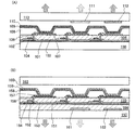
図1(A)に本発明の発光装置の構成の一例を示す。図1(A)はアクティブマトリクス型の発光装置の画素部における断面図の一部である。図1(A)に示した本発明の発光装置は基板100、下地絶縁膜101、半導体層102、ゲート絶縁膜103、ゲート電極104、層間絶縁膜105、接続部106、発光素子の第1の電極107、隔壁108、有機化合物を含む層109、発光素子の第2の電極110、色変換層(緑)111、色変換層(赤)112、対向基板113の構成を含む。なお、図1では、シール材を省略した。
(Embodiment 1)
FIG. 1A illustrates an example of a structure of the light-emitting device of the present invention. FIG. 1A is a part of a cross-sectional view of a pixel portion of an active matrix light-emitting device. A light-emitting device of the present invention illustrated in FIG. 1A includes a
発光素子は、発光素子の第1の電極107と第2の電極110との間に有機化合物を含む層109が挟まれている部分に形成される。発光素子は第1の電極107と電気的に接触する接続部106を介して半導体層102、ゲート絶縁膜103、ゲート電極104よりなる薄膜トランジスタに接続され、発光の制御がなされる。また、本実施の形態において、第1の電極107は反射率の高い材料により形成された反射電極とし、第2の電極110は透光性を有する導電材料により形成された透明電極とし、第2の電極110の方向から光を射出する構成となっている。
The light-emitting element is formed in a portion where the layer 109 containing an organic compound is sandwiched between the
本実施の形態において、発光素子から発する光は近紫外領域〜青緑領域の光である。発光素子からの発光を発光装置外部に射出する際に、色変換層(緑)111、色変換層(赤)112を介して緑や赤の光を射出し、青色の光は、色変換層を介さず発光装置外部に射出することで、赤、緑、青の3色の光を得ることができる。色変換層はある波長帯の光を吸収し、吸収した波長の光より波長の長い波長帯の光を発する層である。 In this embodiment mode, light emitted from the light emitting element is light in the near ultraviolet region to blue-green region. When light emitted from the light emitting element is emitted outside the light emitting device, green or red light is emitted through the color conversion layer (green) 111 and the color conversion layer (red) 112, and the blue light is emitted from the color conversion layer. By emitting the light to the outside of the light emitting device without going through the light, it is possible to obtain light of three colors of red, green, and blue. The color conversion layer is a layer that absorbs light in a certain wavelength band and emits light in a wavelength band longer than the absorbed wavelength light.
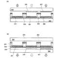
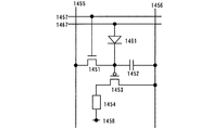
また、有機化合物を含む層109は図2(A)に示したような積層構造を有している。なお、図2(A)の第1の電極400は図1(A)の第1の電極107、図2(A)の第2の電極403は図1(A)の第2の電極110に相当する。また、図2(A)におけるバッファ層401と発光層402の積層が図1(A)における有機化合物を含む層109に相当する。即ち、有機化合物を含む層109はバッファ層401と発光層402との積層からなる。また、バッファ層は反射電極である第1の電極107側に設けられる。
In addition, the layer 109 containing an organic compound has a stacked structure as shown in FIG. Note that the
まず、発光層402について説明する。発光層402は少なくとも発光物質を含む層を有する単層もしくは積層構造よりなる層である。発光層402の詳しい積層構造については図3(A)〜(D)に示した。図3(A)〜(D)において、410が正孔注入性を有する材料で形成した正孔注入層、411が正孔輸送性を有する材料を用いた正孔輸送層、412が電子輸送性を有する材料を用いた電子輸送層、413が電子注入性を有する材料を用いた電子注入層を表す。また、420、422、424、426は発光物質を含む層、421、423、425は発光領域を表している。なお、これらの層の他に電子と正孔が発光物質を含む層において効率よく再結合することが出来るようにする為のブロッキング層等、他の機能を有する層が形成されていても良い。
First, the
正孔注入層410、正孔輸送層411、電子輸送層412、電子注入層413は各々設けても設けなくとも良く、また、複数の機能を同時に有する層として形成しても良い。なお、バッファ層401と発光物質を含む層420、422、424、426は離れて形成されていることが望ましい。
The
発光物質を含む層の構成としては大きく分けて2種類の構成が挙げられる。すなわち、一つは発光物質(ドーパント)が当該発光物質よりバンドギャップの大きい材料(ホスト)中に分散されてなるホスト−ゲスト型、もう一つは発光物質のみで構成された型である。本発明はそのどちらの構成も適用することができる。 As the structure of the layer containing the light emitting substance, there are roughly two kinds of structures. That is, one is a host-guest type in which a light-emitting substance (dopant) is dispersed in a material (host) having a band gap larger than that of the light-emitting substance, and the other is a type composed of only a light-emitting substance. Either of the configurations can be applied to the present invention.
続いてバッファ層401について説明する。バッファ層401は、その厚みを調節することにより反射電極で反射され戻ってくる光の光路長を調節する役割を有する。反射電極で反射され、戻ってきた光は直接発光素子外部に射出する光と干渉を起こす。バッファ層の401の厚みを調節し、直接発光素子外部に射出する光と反射電極で反射され戻ってくる光の位相を合わせることによって発光を増幅し、同じ電流を流した場合により大きな輝度を得ることができるようになる。すなわち、発光効率を向上させることができるようになる。
Next, the
また、光の位相を合わせることはある特定の波長においてなされるため、色純度も向上する。すなわち、発光層の発光スペクトルがシャープになる。したがって、色変換層の吸収スペクトルに、該発光スペクトルを合わせこむことで、色変換層は発光層からの発光を効率よく吸収することができる。その結果、発光効率を向上させることができる。 Further, since the phase of light is adjusted at a specific wavelength, the color purity is also improved. That is, the emission spectrum of the light emitting layer becomes sharp. Therefore, by matching the emission spectrum with the absorption spectrum of the color conversion layer, the color conversion layer can efficiently absorb light emitted from the light emitting layer. As a result, luminous efficiency can be improved.
また、バッファ層401は正孔輸送性を有する有機化合物と金属化合物との複合材料によって形成される。金属化合物としては、遷移金属の酸化物や窒化物が望ましく、4〜8族に属する金属の酸化物もしくは窒化物がさらに望ましい。その中でもバナジウム酸化物、タンタル酸化物、モリブデン酸化物、タングステン酸化物、レニウム酸化物及びルテニウム酸化物は好適である。正孔輸送性を有する有機化合物としては4,4’−ビス[N−(1−ナフチル)−N−フェニルアミノ]ビフェニル(略称:NPB)、4,4’−ビス[N−(3−メチルフェニル)−N−フェニルアミノ]ビフェニル(略称:TPD)、4,4’,4’’−トリス(N,N−ジフェニルアミノ)トリフェニルアミン(略称:TDATA)、4,4’,4’’−トリス[N−(3−メチルフェニル)−N−フェニルアミノ]トリフェニルアミン(略称:MTDATA)、4,4’−ビス{N−[4−(N,N−ジ−m−トリルアミノ)フェニル]−N−フェニルアミノ}ビフェニル(略称:DNTPD)、1,3,5−トリス[N,N−ジ(m−トリル)アミノ]ベンゼン(略称:m−MTDAB)、4,4’,4’’−トリス(N−カルバゾリル)トリフェニルアミン(略称:TCTA)等のアリールアミノ基を有する有機材料や、フタロシアニン(略称:H2Pc)、銅フタロシアニン(略称:CuPc)、バナジルフタロシアニン(略称:VOPc)等も用いることができる。
The
また、下記一般式(1)で表されるような有機材料も正孔輸送性を有する有機化合物として好適に用いることができ、その具体例としては3−[N−(9−フェニルカルバゾール−3−イル)−N−フェニルアミノ]−9−フェニルカルバゾール(略称:PCzPCA1)、3,6−ビス[N−(9−フェニルカルバゾール−3−イル)−N−フェニルアミノ]−9−フェニルカルバゾール(略称:PCzPCA2)等を挙げることができる。この構造を有する有機化合物を用いた第1の複合材料は熱的安定性に優れ、信頼性が良い。 In addition, an organic material represented by the following general formula (1) can also be suitably used as the organic compound having a hole transporting property, and specific examples thereof include 3- [N- (9-phenylcarbazole-3]. -Yl) -N-phenylamino] -9-phenylcarbazole (abbreviation: PCzPCA1), 3,6-bis [N- (9-phenylcarbazol-3-yl) -N-phenylamino] -9-phenylcarbazole ( Abbreviations: PCzPCA2) and the like. The first composite material using an organic compound having this structure has excellent thermal stability and good reliability.

また、下記一般式(3)乃至(6)のいずれかで示されるような有機材料も好適に用いることができる。下記一般式(3)乃至(6)のいずれかで表される有機化合物の具体例としては、N−(2−ナフチル)カルバゾール(略称:NCz)、4,4’−ジ(N−カルバゾリル)ビフェニル(略称:CBP)、9,10−ビス[4−(N−カルバゾリル)フェニル]アントラセン(略称:BCPA)、3,5−ビス[4−(N−カルバゾリル)フェニル]ビフェニル(略称:BCPBi)、1,3,5−トリス[4−(N−カルバゾリル)フェニル]ベンゼン(略称:TCPB)等を挙げることができる。 An organic material represented by any one of the following general formulas (3) to (6) can also be suitably used. Specific examples of the organic compound represented by any one of the following general formulas (3) to (6) include N- (2-naphthyl) carbazole (abbreviation: NCz), 4,4′-di (N-carbazolyl). Biphenyl (abbreviation: CBP), 9,10-bis [4- (N-carbazolyl) phenyl] anthracene (abbreviation: BCPA), 3,5-bis [4- (N-carbazolyl) phenyl] biphenyl (abbreviation: BCPBi) 1,3,5-tris [4- (N-carbazolyl) phenyl] benzene (abbreviation: TCPB) and the like.
さらに、アントラセン、9,10−ジフェニルアントラセン(略称:DPA)、2−tert−ブチル−9,10−ジ(2−ナフチル)アントラセン(略称:t−BuDNA)、テトラセン、ルブレン、ペンタセン等の芳香族炭化水素も用いることができる。 Furthermore, aromatics such as anthracene, 9,10-diphenylanthracene (abbreviation: DPA), 2-tert-butyl-9,10-di (2-naphthyl) anthracene (abbreviation: t-BuDNA), tetracene, rubrene, pentacene, etc. Hydrocarbons can also be used.
バッファ層401は上述した金属化合物と正孔輸送性を有する有機化合物とを共蒸着することによって作製することができるが、湿式法やその他のどの方法によって形成されていても良い。なお、バッファ層401において有機化合物と金属化合物とは質量比で95:5〜20:80、さらには90:10〜50:50であることが望ましい。
The
なお、バッファ層401を発光層402に対して陰極として機能する電極側に設ける場合は、バッファ層401を2層構造として形成することが好ましい。具体的には電子を発生する機能を有する層を発光層402に接するように設ける。電子を発生する機能を有する層は、透明導電材料や、電子輸送性を有する有機化合物と無機化合物との複合材料で形成すればよい。無機化合物としてはアルカリ金属及びアルカリ土類金属、もしくはそれらを含む酸化物や窒化物が望ましく、具体的には、リチウム、ナトリウム、カリウム、セシウム、マグネシウム、カルシウム、ストロンチウム、バリウム、リチウム酸化物、マグネシウム窒化物、カルシウム窒化物であることが好ましい。また、電子輸送性を有する有機化合物としては、例えば、トリス(8−キノリノラト)アルミニウム(略称:Alq3)、トリス(4−メチル−8−キノリノラト)アルミニウム(略称:Almq3)、ビス(10−ヒドロキシベンゾ[h]−キノリナト)ベリリウム(略称:BeBq2)、ビス(2−メチル−8−キノリノラト)−4−フェニルフェノラト−アルミニウム(略称:BAlq)等キノリン骨格またはベンゾキノリン骨格を有する金属錯体等からなる材料を用いることができる。また、この他、ビス[2−(2−ヒドロキシフェニル)ベンゾオキサゾラト]亜鉛(略称:Zn(BOX)2)、ビス[2−(2−ヒドロキシフェニル)ベンゾチアゾラト]亜鉛(略称:Zn(BTZ)2)などのオキサゾール系、チアゾール系配位子を有する金属錯体などの材料も用いることができる。さらに、金属錯体以外にも、2−(4−ビフェニリル)−5−(4−tert−ブチルフェニル)−1,3,4−オキサジアゾール(略称:PBD)、1,3−ビス[5−(p−tert−ブチルフェニル)−1,3,4−オキサジアゾール−2−イル]ベンゼン(略称:OXD−7)、3−(4−tert−ブチルフェニル)−4−フェニル−5−(4−ビフェニリル)−1,2,4−トリアゾール(略称:TAZ)、3−(4−tert−ブチルフェニル)−4−(4−エチルフェニル)−5−(4−ビフェニリル)−1,2,4−トリアゾール(略称:p−EtTAZ)、バソフェナントロリン(略称:BPhen)、バソキュプロイン(略称:BCP)等を用いることができる。
Note that in the case where the
バッファ層401の厚みは発光装置の発光効率が向上するように設定される。具体的には、発光領域と反射電極との光学的距離L、目的とする波長をλとするとL=(2m−1)λ/4(但しmは1以上の自然数)を満たすようにする。また、発光領域と反射電極との光学的距離Lは、発光層402とバッファ層401との界面から第1の電極400までの距離をd1、発光層402と第2の電極403との界面から第1の電極400までの距離をd2(ただし、d1<d2)としたとき、d1≦L≦d2の範囲で規定される。材料の異なる複数の層が存在する場合は各々の光学的距離の和が上記式を満たすようにする。光学的距離は「実際の距離×波長λにおける屈折率」で算出される。
The thickness of the
なお、バッファ層401の膜厚が非常に厚い構成であったり、バッファ層401の導電率が高かったりした場合、発光素子の形成密度によっては隣接する素子間でクロストークが発生してしまうことが考えられる。このような場合は、バッファ層401のみパターン形成し、画素毎に独立して設けるのがよい。但し、このようなクロストークは、通常の構成であればあまり問題にならない。
Note that when the
発光領域は発光物質を含む層のどこかに存在するがそれを厳密に決定することは困難である。しかし、発光物質を含む層の任意の位置を発光領域と仮定することで充分に本発明の効果を得ることができる。なお、さらに厳密に発光領域の特定を行いたい場合は以下のように発光領域の位置を見積もることによってより正確な光学調整を行うことができる。 The light emitting region exists somewhere in the layer containing the light emitting substance, but it is difficult to determine it precisely. However, the effect of the present invention can be sufficiently obtained by assuming an arbitrary position of the layer containing the light emitting material as the light emitting region. If it is desired to specify the light emitting area more strictly, more accurate optical adjustment can be performed by estimating the position of the light emitting area as follows.
図3(A)〜(D)は発光物質を含む層のホスト材料によって発光領域がどの位置に来るのかを示した概略図である。なお、図3(A)〜(C)の発光物質を含む層はホスト−ゲスト型、図3(D)の発光物質を含む層は発光物質のみで形成された型を示した。 FIGS. 3A to 3D are schematic views showing where the light emitting region comes depending on the host material of the layer containing the light emitting substance. 3A to 3C show the host-guest type, and the layer containing the luminescent material in FIG. 3D shows a type formed only of the luminescent material.
図3(A)は発光物質を含む層420のホスト材料が電子輸送性の材料で形成されている場合を示した図である。この場合、発光領域421は、発光物質を含む層420の正孔輸送層411に近い側に形成されると考えられる。図3(B)は発光物質を含む層422のホスト材料が正孔輸送性の材料で形成されている場合を示した図である。この場合、発光領域423は発光物質を含む層422のホスト材料が電子輸送層412に近い側に形成されると考えられる。図3(C)は発光物質を含む層424のホスト材料がバイポーラ性の材料で形成されている場合を示した図である。この場合、発光領域425の位置の見積もりは困難であるので、発光物質を含む層424の真ん中を発光領域425と仮定するか、使用したホスト材料のキャリア輸送性のバランスを考慮してホスト材料の正孔輸送性が電子輸送性より高い場合は電子輸送層412側に、逆の場合は正孔輸送層411側に発光領域425を若干ずらして仮定すると良い。図3(D)は発光物質のみで発光物質を含む層426が形成されている場合を示した図である。この場合、発光物質が正孔輸送性を有していれば発光領域は電子輸送層側に、電子輸送性を有していれば発光領域は正孔輸送層側に偏ると考えられるが、図3(C)同様、発光領域位置の見積もりは困難であるので、発光物質を含む層426の真ん中を発光領域と仮定するか、発光物質のキャリア輸送性のバランスを考慮してホスト材料の正孔輸送性が電子輸送性より高い場合は電子輸送層412側に、逆の場合は正孔輸送層411側に発光領域425を若干ずらして仮定すると良い。なお、このような見積もりによらずとも、他の実験などにおいて発光領域の位置が確定している場合はそれを用いれば良い。
FIG. 3A illustrates a case where the host material of the
上述した複合材料は、その膜厚を厚く形成しても駆動電圧の上昇が起こらないため、バッファ層401として非常に好適に用いることができる。このような複合材料をバッファ層401とした発光素子を用いた本発明発光素子は、大幅な駆動電圧の上昇を招かずに光の光路長を制御することができ、発光効率や色純度が良く、且つ駆動電圧の低い発光装置である。
The above-described composite material can be used very favorably as the
一対の電極間に有機化合物を含む層を挟んでなる発光素子を用いた発光装置の大きな問題点の一つは発光素子の寿命、すなわち長期使用における信頼性である。発光効率が高いと、発光効率の低い発光装置と比較して小さい電流密度で同じ輝度を得ることができるため、発光装置の寿命を延ばすことができ、長期使用における信頼性が向上する。また、駆動電圧は特にモバイル機器用途での使用が有望視されている発光装置においては非常に重要なファクターである。これらのことから発光効率が高く、駆動電圧が低い本発明の発光装置は特にモバイル機器用途において非常に大きなメリットを有する。 One of the major problems of a light-emitting device using a light-emitting element in which a layer containing an organic compound is sandwiched between a pair of electrodes is the life of the light-emitting element, that is, reliability in long-term use. When the light emission efficiency is high, the same luminance can be obtained with a small current density as compared with a light emission device with low light emission efficiency, so that the life of the light emission device can be extended and the reliability in long-term use is improved. In addition, the driving voltage is a very important factor particularly in a light-emitting device that is expected to be used in mobile device applications. For these reasons, the light-emitting device of the present invention having high luminous efficiency and low driving voltage has a great advantage especially in mobile device applications.
本実施の形態におけるその他の構成について説明する。図1における基板100及び対向基板113は薄膜トランジスタや発光素子の支持体として用いられ、その材料としてはガラス、石英やプラスチック(ポリイミド、アクリル、ポリエチレンテレフタラート、ポリカーボネート、ポリアクリレート、ポリエーテルスルホンなど)等を用いることができるが、その他薄膜トランジスタや発光素子の支持体として用いることが出来るものであればこれら以外の材料で形成されていても良い。また、基板は必要に応じてCMP等により研磨されていても良い。
Other configurations in the present embodiment will be described. The
基板100と半導体層102との間には下地絶縁膜が単層もしくは多層で設けられていても良い。下地絶縁膜は、基板100中のアルカリ金属やアルカリ土類金属など、半導体膜の特性に悪影響を及ぼすような元素が半導体層中に拡散するのを防ぐ為に設ける。材料としては酸化ケイ素、窒化ケイ素、窒素を含む酸化ケイ素、酸素を含む窒化ケイ素などを用いることができる。なお、基板からの不純物の拡散が気にならないようであれば下地絶縁層は設ける必要がない。
A base insulating film may be provided as a single layer or a multilayer between the
薄膜トランジスタは本発明ではトップゲート型の薄膜トランジスタの例を示したが、ボトムゲート型(逆スタガ型)など他の既存の薄膜トランジスタでも良く、本発明は発光素子を駆動するトランジスタの種類及び駆動方法によって限定されることはない。 In the present invention, an example of a top gate type thin film transistor is shown in the present invention, but other existing thin film transistors such as a bottom gate type (reverse stagger type) may be used, and the present invention is limited by the type and driving method of the transistor driving the light emitting element. It will never be done.
層間絶縁膜105は薄膜トランジスタと発光素子が不要な部分において電気的に接触することを防ぐ為に設けられ、単層であっても多層であっても良い。層間絶縁膜105は少なくとも一層が下部の薄膜トランジスタなどにより発生した凹凸を緩和できるような自己平坦性を有する材料で形成することが好ましい。例えば、アクリル、ポリイミド、もしくはケイ素と酸素との結合で骨格構造が構成され、置換基として少なくとも水素を含む有機基(例えばアルキル基、アリール基)、フルオロ基、又は少なくとも水素を含む有機基及びフロオロ基を有する材料、いわゆるシロキサンなどの材料を用いることが望ましい。また、その他の材料としては酸化ケイ素、窒化ケイ素、窒化ケイ素を含む酸化ケイ素、酸化ケイ素を含む窒化ケイ素、低誘電率材料等を用いて形成することができる。
The
発光素子の第1の電極107及び第2の電極110は金属、合金、電気伝導性化合物、およびこれらの混合物を用いることができる。例えば、アルミニウム(Al)、銀(Ag)、金(Au)、白金(Pt)、ニッケル(Ni)、タングステン(W)、クロム(Cr)、モリブデン(Mo)、鉄(Fe)、コバルト(Co)、銅(Cu)、パラジウム(Pd)、リチウム(Li)、セシウム(Cs)、マグネシウム(Mg)、カルシウム(Ca)、ストロンチウム(Sr)、チタン(Ti)などの導電性を有する金属、又はアルミニウム−ケイ素(Al−Si)、アルミニウム−チタン(Al−Ti)、アルミニウム−ケイ素−銅(Al−Si−Cu)等それらの合金、または窒化チタン(TiN)等の金属材料の窒化物、インジウム錫酸化物(ITO:Indium Tin Oxide)、酸化ケイ素を含有するインジウム錫酸化物(ITSO)、酸化インジウムに2〜20wt%の酸化亜鉛(ZnO)を混合した酸化インジウム酸化亜鉛(IZO:Indium Zinc Oxide)等の金属化合物などを用いることができるが、第1の電極107を発光素子が発光する際に高い電圧がかかる方の電極(陽極として機能する電極)とする場合には、その中でも、仕事関数の大きい(仕事関数4.0eV以上)材料で形成されていることが好ましい。また、第1の電極107を発光素子が発光する際に低い電圧がかかる方の電極(陰極として機能する電極)とする場合にはその中でも、仕事関数の小さい(仕事関数3.8eV以下)材料で形成されていることが好ましい。
For the
なお、発光を取り出す側の電極はITOやITSO、IZOなどの透光性を有する導電材料で形成することが望ましい。なお、アルミニウムや銀など厚膜で形成すると非透光性であるが、薄膜化すると透光性を有するようになるため、アルミニウムや銀の薄膜を透光性を有する電極として用いることもできる。本実施の形態では発光素子の第2の電極110側から発光を取り出すため、第2の電極110を透光性を有する導電材料で形成する。また、反射電極となる電極はアルミニウムや銀などの反射率の高い導電材料(発光層から発する光に対する反射率が70%以上)を用いることが望ましい。もちろん、反射電極としてアルミニウム、銀を使用する時は透光性を有さない程度に厚膜化して形成する。
Note that the electrode from which light is extracted is preferably formed using a light-transmitting conductive material such as ITO, ITSO, or IZO. In addition, although it is non-light-transmitting when formed with a thick film such as aluminum or silver, it becomes light-transmitting when it is thinned, so that a thin film of aluminum or silver can also be used as a light-transmitting electrode. In this embodiment mode, the
有機化合物を含む層109は図2に示したようにバッファ層401と発光層402で構成される。バッファ層401の構成は前述した通りである。発光層402は少なくとも発光物質を含む層を含む単層もしくは積層からなる層である。
The layer 109 containing an organic compound includes a
発光層402の積層構造は、図3に示したように機能分離型の積層構造が代表的である。正孔と電子が再結合する発光物質を含む層を挟んで正孔の輸送性が高い材料による層を陽極として機能する電極側に、電子の輸送性が高い材料による層を陰極側に配置することによって効率良く正孔及び電子の輸送を行うことが出来、さらに正孔及び電子が再結合する確率も高めることができる。
The laminated structure of the
正孔注入層410を形成するのに用いることのできる物質の具体例として、フタロシアニン(略称:H2Pc)や銅フタロシアニン(略称:CuPC)等のフタロシアニン系の化合物、或いはポリ(エチレンジオキシチオフェン)/ポリ(スチレンスルホン酸)水溶液(PEDOT/PSS)等の高分子等が挙げられる。正孔注入層に用いる材料のイオン化ポテンシャルが、正孔輸送層のイオン化ポテンシャルよりも相対的に小さくなるような物質を、正孔輸送性を有する物質の中から選択することによって、正孔注入層を形成することができる。
Specific examples of a substance that can be used to form the hole-injecting
正孔輸送層411を形成するのに用いることができる物質の具体例としては、4,4’−ビス[N−(1−ナフチル)−N−フェニルアミノ]ビフェニル(略称:α−NPD)、4,4’−ビス[N−(3−メチルフェニル)−N−フェニルアミノ]ビフェニル(略称:TPD)、4,4’,4’’−トリス(N,N−ジフェニルアミノ)トリフェニルアミン(略称:TDATA)、4,4’,4’’−トリス[N−(3−メチルフェニル)−N−フェニルアミノ]トリフェニルアミン(略称:MTDATA)、4,4’−ビス{N−[4−(N,N−ジ−m−トリルアミノ)フェニル]−N−フェニルアミノ}ビフェニル(略称:DNTPD)、1,3,5−トリス[N,N−ジ(m−トリル)アミノ]ベンゼン(略称:m−MTDAB)、4,4’,4’’−トリス(N−カルバゾリル)トリフェニルアミン(略称:TCTA)、フタロシアニン(略称:H2Pc)、銅フタロシアニン(略称:CuPc)、バナジルフタロシアニン(略称:VOPc)等が挙げられる。また、正孔輸送層は、以上に述べた物質から成る層を二以上組み合わせて形成した多層構造の層であってもよい。
Specific examples of a substance that can be used to form the hole-
また、正孔輸送層411を設けることによって、第1の電極107と発光物質を含む層との距離を離すことができ、第1の電極107に含まれている金属に起因して発光が消光することを防ぐことができる。正孔輸送層411は、正孔輸送性の高い物質を用いて形成することが好ましく、特に10〜1×10⁻⁶cm2/Vsの正孔移動度を有する物質を用いて形成することが好ましい。
In addition, by providing the hole-
発光物質を含む層420、422、424、426として機能する層には大きく分けて2つの態様がある。一つは発光中心となる発光物質の有するエネルギーギャップよりも大きいエネルギーギャップを有する材料(ホスト材料)からなる層に発光材料を分散して含むホスト−ゲスト型の層(420、422、424)と、もう一つは発光物質のみで発光層を構成する層(426)であるが、前者は濃度消光が起こりにくく、好ましい構成である。本発明の発光装置においては発光層から近紫外領域〜青緑領域の光を発する様な構成を選択する。このような発光材料としては、クマリン誘導体、オリゴフェニレン誘導体、オキサゾール誘導体、スチルベン誘導体、キノロン誘導体、アクリドン誘導体、アントラセン誘導体、ピレン誘導体、フェナントレン誘導体、ピレン誘導体などが好適である。これらのドーパントを少量、具体的にはホスト材料に対して0.001から50wt%、好ましくは0.03から20wt%の割合で添加する。また、上記発光材料を分散してなる層を形成する場合に母体となるホスト材料としては、テトラアリールシラン誘導体、ジナフタレン誘導体、ピレン誘導体、オリゴチオフェン誘導体、ベンゾフェノン誘導体、ベンゾニトリル誘導体等などが挙げられる。
The layers functioning as the
電子輸送層412を形成するのに用いることができる物質の具体例としては、トリス(8−キノリノラト)アルミニウム(略称:Alq3)、トリス(4−メチル−8−キノリノラト)アルミニウム(略称:Almq3)、ビス(10−ヒドロキシベンゾ[h]−キノリナト)ベリリウム(略称:BeBq2)、ビス(2−メチル−8−キノリノラト)−4−フェニルフェノラト−アルミニウム(略称:BAlq)、ビス[2−(2−ヒドロキシフェニル)ベンゾオキサゾラト]亜鉛(略称:Zn(BOX)2)、ビス[2−(2−ヒドロキシフェニル)ベンゾチアゾラト]亜鉛(略称:Zn(BTZ)2)等の他、2−(4−ビフェニリル)−5−(4−tert−ブチルフェニル)−1,3,4−オキサジアゾール(略称:PBD)、1,3−ビス[5−(p−tert−ブチルフェニル)−1,3,4−オキサジアゾール−2−イル]ベンゼン(略称:OXD−7)、3−(4−ビフェニリル)−4−フェニル−5−(4−tert−ブチルフェニル)−1,2,4−トリアゾール(略称:TAZ)、3−(4−ビフェニリル)−4−(4−エチルフェニル)−5−(4−tert−ブチルフェニル)−1,2,4−トリアゾール(略称:p−EtTAZ))、バソフェナントロリン(略称:BPhen)、バソキュプロイン(略称:BCP)、2,2’,2’’−(1,3,5−ベンゼントリイル)−トリス(1−フェニル−1H−ベンゾイミダゾール)(略称:TPBI)、4,4−ビス(5−メチルベンズオキサゾル−2−イル)スチルベン(略称:BzOs)等が挙げられる。また、電子輸送層は、以上に述べた物質から成る層を二以上組み合わせて形成した多層構造の層であってもよい。 Specific examples of a substance that can be used for forming the electron-transport layer 412 include tris (8-quinolinolato) aluminum (abbreviation: Alq 3 ), tris (4-methyl-8-quinolinolato) aluminum (abbreviation: Almq 3). ), Bis (10-hydroxybenzo [h] -quinolinato) beryllium (abbreviation: BeBq 2 ), bis (2-methyl-8-quinolinolato) -4-phenylphenolato-aluminum (abbreviation: BAlq), bis [2- In addition to (2-hydroxyphenyl) benzoxazolate] zinc (abbreviation: Zn (BOX) 2 ), bis [2- (2-hydroxyphenyl) benzothiazolate] zinc (abbreviation: Zn (BTZ) 2 ), etc., 2- (4-Biphenylyl) -5- (4-tert-butylphenyl) -1,3,4-oxadiazole (abbreviation: PBD) ), 1,3-bis [5- (p-tert-butylphenyl) -1,3,4-oxadiazol-2-yl] benzene (abbreviation: OXD-7), 3- (4-biphenylyl)- 4-phenyl-5- (4-tert-butylphenyl) -1,2,4-triazole (abbreviation: TAZ), 3- (4-biphenylyl) -4- (4-ethylphenyl) -5- (4- tert-butylphenyl) -1,2,4-triazole (abbreviation: p-EtTAZ)), bathophenanthroline (abbreviation: BPhen), bathocuproin (abbreviation: BCP), 2,2 ′, 2 ″-(1,3 , 5-benzenetriyl) -tris (1-phenyl-1H-benzimidazole) (abbreviation: TPBI), 4,4-bis (5-methylbenzoxazol-2-yl) stilbene (abbreviation: BzOs), and the like. It is below. The electron transport layer may be a layer having a multilayer structure formed by combining two or more layers made of the substances described above.
また、電子輸送層412を設けることによって、第2の電極110と発光層との距離を離すことができ、第2の電極110に含まれている金属に起因して発光が消光することを防ぐことができる。電子輸送層412は、電子輸送性の高い物質を用いて形成することが好ましく、特に10〜1×10⁻⁶cm2/Vsの電子移動度を有する物質を用いて形成することが好ましい。
In addition, by providing the
電子注入層413を形成するのに用いることができる物質の具体例としては、アルカリ金属またはアルカリ土類金属、アルカリ金属のフッ化物、アルカリ土類金属のフッ化物、アルカリ金属の酸化物、アルカリ土類金属の酸化物等の無機物が挙げられる。また、無機物の他、BPhen、BCP、p−EtTAZ、TAZ、BzOs等の電子輸送層を形成するのに用いることのできる物質も、これらの物質の中から、電子輸送層の形成に用いる物質よりも電子親和力が大きい物質を選択することによって、電子注入層を形成する物質として用いることができる。つまり、電子注入層における電子親和力が電子輸送層における電子親和力よりも相対的に大きくなるような物質を電子輸送性を有する物質の中から選択することによって、電子注入層を形成することもできる。
Specific examples of a substance that can be used to form the
発光素子の第1の電極107は隔壁108によってその端部が覆われており、隔壁108より第1の電極107が露出している部分が当該発光素子の発光領域となる。隔壁108は層間絶縁膜105の材料として挙げた材料と同様の材料を使用することができる。
The edge of the
発光素子の第1の電極107と薄膜トランジスタとを電気的に接続する接続部106はアルミニウム、銅、アルミニウムと炭素とニッケルの合金、アルミニウムと炭素とモリブデンの合金等の単層や多層で形成する。多層構造の場合例えば、薄膜トランジスタ側からモリブデン、アルミニウム、モリブデンやチタン、アルミニウム、チタンもしくはチタン、窒化チタン、アルミニウム、チタンといった積層構造等が考えられる。
The
発光装置は基板100上に形成された上記素子を図示しないシール材を用いて対向基板113により外部雰囲気から封止することによって完成する。対向基板113には各発光素子に対応して色変換層(緑)111、色変換層(赤)112が設けられている。発光素子から発した光は当該色変換層(緑)111もしくは色変換層(赤)112に入射し、色変換層が発光素子からの光を吸収し、フォトルミネッセンスを発することで緑、赤の発光色を得ることができ、発光素子から発する青、色変換層で変換された緑、赤の3色よりなるフルカラー表示を行う発光装置を得ることができる。対向基板113は基板100と同様の材料を用いることができる。
The light-emitting device is completed by sealing the element formed on the
色変換層については、本実施の形態では青色領域の光を吸収して赤色領域の蛍光を発する物質を有する層、青色領域の光を吸収して緑色領域の蛍光を発する物質を含有する層の2種類を用いる。青色領域の光を吸収して赤色領域の蛍光を発する物質としては、例えばローダミンB、ローダミン6G、ローダミン3B、ローダミン101、ローダミン110、スルホローダミン、ベーシックバイオレット11、ベーシックレッド2等のローダミン系色素、シアニン系色素、1−エチル−2−[4−(p−ジメチルアミノフェニル)−1,3−ブタジエニル]ピリジニウムパークロレート(ピリジン1)等のピリジン系の色素、オキサジン系色素等が挙げられる。さらに各種染料も青色領域の光を吸収して赤色領域の蛍光を発する性質を有していれば使用することができる。青色領域の光を吸収して緑色領域の蛍光を発する物質としては、例えば、クマリン6、クマリン7、クマリン30、クマリン153等のクマリン系色素、ベーシックイエロー51等のクマリン色素系染料、ソルベントイエロー11、ソルベントイエロー116等のナフタルイミド系染料などが挙げられる。さらに各種染料も青色領域の光を吸収して緑色領域の蛍光を発する性質を有していれば使用することができる。
Regarding the color conversion layer, in this embodiment, a layer having a substance that absorbs light in the blue region and emits fluorescence in the red region, and a layer that contains a substance that absorbs light in the blue region and emits fluorescence in the green region. Two types are used. Examples of the substance that absorbs light in the blue region and emits fluorescence in the red region include rhodamine dyes such as rhodamine B, rhodamine 6G, rhodamine 3B,
色変換層を溶解、もしくは分散させる基材となる樹脂としては、ポリメチルメタクリレート樹脂、ポリアクリレート樹脂、ポリカーボネート樹脂、ポリビニルアルコール樹脂、ポリビニルピロリドン樹脂、ヒドロキシエチルセルロース樹脂、カルボキシメチルセルロース樹脂、ポリ塩化ビニル樹脂、メラミン樹脂、フェノール樹脂、アルキッド樹脂、エポキシ樹脂、ポリウレタン樹脂、ポリエステル樹脂、マレイン酸樹脂、ポリアミド樹脂などの透明樹脂をもちいることができる。また、アクリレート系、メタクリレート系、ポリ桂皮酸ビニル系もしくは環化ゴム系の反応性ビニル基を有する電離放射線硬化性樹脂も用いることができる。 Examples of the resin serving as a base material for dissolving or dispersing the color conversion layer include polymethyl methacrylate resin, polyacrylate resin, polycarbonate resin, polyvinyl alcohol resin, polyvinyl pyrrolidone resin, hydroxyethyl cellulose resin, carboxymethyl cellulose resin, polyvinyl chloride resin, Transparent resins such as melamine resin, phenol resin, alkyd resin, epoxy resin, polyurethane resin, polyester resin, maleic acid resin, and polyamide resin can be used. An ionizing radiation curable resin having a reactive vinyl group of acrylate type, methacrylate type, polyvinyl cinnamate type or cyclized rubber type can also be used.
以上の様な構成を有する本発明の発光装置は、バッファ層を厚く形成しても大幅な駆動電圧の上昇を招かないため、発光素子内で光の光路長を制御することで、発光効率や色純度が良く、且つ駆動電圧の低い発光装置とすることができる。 The light-emitting device of the present invention having the above-described configuration does not cause a significant increase in driving voltage even when the buffer layer is formed thick. Therefore, by controlling the optical path length of light in the light-emitting element, A light emitting device with high color purity and low driving voltage can be obtained.
一対の電極間に有機化合物を含む層を挟んでなる発光素子を用いた発光装置の大きな問題点の一つは発光素子の寿命、すなわち長期使用における信頼性である。発光効率が高いと、発光効率の低い発光装置と比較して小さい電流密度で同じ輝度を得ることができるため、発光装置の寿命を延ばすことができ、長期使用における信頼性が向上する。また、駆動電圧は特にモバイル機器用途での使用が有望視されている発光装置においては非常に重要なファクターである。これらのことから発光効率が高く、駆動電圧が低い本発明の発光装置は特にモバイル機器用途において非常に大きなメリットを有する。 One of the major problems of a light-emitting device using a light-emitting element in which a layer containing an organic compound is sandwiched between a pair of electrodes is the life of the light-emitting element, that is, reliability in long-term use. When the light emission efficiency is high, the same luminance can be obtained with a small current density as compared with a light emission device with low light emission efficiency, so that the life of the light emission device can be extended and the reliability in long-term use is improved. In addition, the driving voltage is a very important factor particularly in a light-emitting device that is expected to be used in mobile device applications. For these reasons, the light-emitting device of the present invention having high luminous efficiency and low driving voltage has a great advantage especially in mobile device applications.
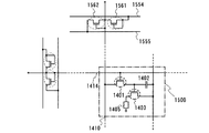
(実施の形態2)
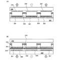
図1(B)は図1(A)と異なる構成を有する本発明の発光装置を表す図である。図1(B)に示した本発明の発光装置は、基板150、下地絶縁膜151、半導体層152、ゲート絶縁膜153、ゲート電極154、層間絶縁膜155、接続部156、発光素子の第1の電極157、隔壁158、有機化合物を含む層159、発光素子の第2の電極160、色変換層(緑)161、色変換層(赤)162、対向基板163、凹凸緩和層164の構成を含む。本実施の形態では、発光素子の第1の電極157側に発光素子が光を射出する構成のボトムエミッション型の発光装置の例を示した。本実施の形態では第1の電極157側から発光を取り出す為、第1の電極157を透光性を有する導電材料で形成し、第2の電極160を反射電極として反射率の高い導電材料(発光層から発する光に対する反射率が70%以上)を用いて作製する。これらの具体的な材料については実施の形態1の記載を参照すればよい。
(Embodiment 2)
FIG. 1B illustrates a light-emitting device of the present invention having a structure different from that in FIG. 1B includes a
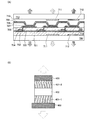
有機化合物を含む層159は図2(B)に示したような積層構造を有している。なお、図2(B)の第1の電極450は図1(B)の第1の電極157、図2(B)の第2の電極453は図1(B)の第2の電極160に相当する。また、図2(B)におけるバッファ層401と発光層402の積層が図1(B)における有機化合物を含む層159に相当する。即ち、有機化合物を含む層159はバッファ層401と発光層402との積層からなる。バッファ層401は反射電極である第2の電極160側に設けられる。この場合、発光領域と反射電極との光学的距離Lは、発光層402とバッファ層401との界面から第2の電極453までの距離をd1、発光層402と第1の電極450との界面から第2の電極453までの距離をd2(ただし、d1<d2)としたとき、d1≦L≦d2の範囲で規定される。
The
本実施の形態では、基板150側から発光を取り出す構造であるため、対向基板163に色変換層は設けず、基板150上に色変換層(緑)161、色変換層(赤)162を形成する。基板上に色変換層を設けたことによって生じる凹凸がその後の素子作製に悪影響を及ぼす場合は、アクリル、ポリイミド、シロキサンなどの自己平坦性を有する材料によって凹凸緩和層164を設けると良い。凹凸緩和層164が良好な絶縁性を有し、且つ充分に基板からの不純物の拡散を抑制できる場合、下地絶縁膜151は設けずとも良い。
In this embodiment mode, light emission is extracted from the
その他の構成及び効果については実施の形態1に記載の通りであるため説明を省略する。実施の形態1の記載を参照されたい。
Since other configurations and effects are the same as those described in the first embodiment, the description thereof is omitted. Refer to the description in
(実施の形態3)
図4(A)は図1(A)と異なる構成を有する本発明の発光装置を表す図である。本実施の形態の構成は実施の形態1の構成とほとんど同じであるが、青色のカラーフィルター115が設けられている点が異なる。発光層からの発光を青色のカラーフィルターを介して射出することによってより色純度を高めた構成とすることができる。発光素子から発する光が青色に近い領域の波長を有するため、光のロスも比較的少ない好ましい構成である。発光素子から発する光を色変換層(緑)111と色変換層(赤)112の吸収に合わせた波長とし、カラーフィルターで青色の色純度を向上させるといった構成も好ましい構成である。なお、図4(A)において、シール材は省略した。
(Embodiment 3)
FIG. 4A illustrates a light-emitting device of the present invention having a structure different from that in FIG. The configuration of the present embodiment is almost the same as the configuration of the first embodiment, except that a
115は近紫外領域〜青領域の光を青色の光に変換する色変換層(青)であっても良い。色変換層(青)は発光素子からの発光を効率よく色純度の高い青色とすることができる。この場合、発光素子からの発光は、得ようとする青色より波長の短いスペクトル成分を有する発光であることが必要である。 115 may be a color conversion layer (blue) that converts light in the near ultraviolet region to blue region into blue light. The color conversion layer (blue) can efficiently emit light from the light emitting element into blue having high color purity. In this case, light emission from the light emitting element needs to be light emission having a spectral component having a shorter wavelength than the blue color to be obtained.
その他の構成及び効果については実施の形態1と同様であるので繰り返しの説明を省略する。実施の形態1の記載を参照されたい。
Other configurations and effects are the same as those of the first embodiment, and thus the repeated description is omitted. Refer to the description in
(実施の形態4)
図4(B)は図1(A)と異なる構成を有する本発明の発光装置を表す図である。本実施の形態の構成は実施の形態2の構成(図1(B)参照)とほとんど同じであるが、青色のカラーフィルター165が設けられている点が異なる。発光層からの発光を青色のカラーフィルターを介して射出することによってより色純度を高めた構成とすることができる。発光素子から発する光が青色に近い領域の波長を有するため、光のロスも比較的少ない好ましい構成である。発光素子から発する光を色変換層(緑)161と色変換層(赤)162の吸収に合わせた波長とし、カラーフィルターで青色の色純度を向上させるといった構成も好ましい構成である。なお、図4(B)において、シール材は省略した。
(Embodiment 4)
FIG. 4B illustrates a light-emitting device of the present invention having a structure different from that in FIG. The configuration of this embodiment is almost the same as the configuration of Embodiment 2 (see FIG. 1B), except that a
165は近紫外領域〜青領域の光を青色の光に変換する色変換層(青)であっても良い。色変換層(青)は発光素子からの発光を効率よく色純度の高い青色とすることができる。この場合、発光素子からの発光は、得ようとする青色より波長の短いスペクトル成分を有する発光であることが必要である。 165 may be a color conversion layer (blue) that converts light in the near ultraviolet region to blue region into blue light. The color conversion layer (blue) can efficiently emit light from the light emitting element into blue having high color purity. In this case, light emission from the light emitting element needs to be light emission having a spectral component having a shorter wavelength than the blue color to be obtained.
その他の構成及び効果については実施の形態2と同様であるので繰り返しの説明を省略する。実施の形態2の記載を参照されたい。
Since other configurations and effects are the same as those of the second embodiment, repeated description is omitted. Refer to the description in
(実施の形態5)
図5(A)に本発明の発光装置の構成の一例を示す。図5(A)は順テーパー構造を有するパッシブマトリクス型の発光装置の画素部における断面図の一部である。図5(A)に示した本発明の発光装置は基板200、発光素子の第1の電極201、隔壁202、有機化合物を含む層203、発光素子の第2の電極204、色変換層(緑)205、色変換層(赤)206、対向基板207の構成を含む。なお、図5(A)において、シール材は省略した。
(Embodiment 5)
FIG. 5A illustrates an example of a structure of the light-emitting device of the present invention. FIG. 5A is a part of a cross-sectional view of a pixel portion of a passive matrix light-emitting device having a forward tapered structure. The light-emitting device of the present invention illustrated in FIG. 5A includes a
発光素子は、発光素子の第1の電極201と第2の電極204とに有機化合物を含む層203が挟まれている部分に形成される。第1の電極201と第2の電極204とは互いに直交するストライプ状に形成され、交差部分に発光素子が形成される。隔壁202は第2の電極204と平行に形成され、発光素子は第1の電極201を同一とする他の発光素子と隔壁202によって絶縁されている。
The light-emitting element is formed in a portion where the
本実施の形態において、第1の電極201は反射率の高い材料(発光層から発する光に対する反射率が70%以上)により形成された反射電極とし、第2の電極204は透光性を有する導電材料により形成された透明電極とし、第2の電極204の方向から光を射出する構成となっている。これらの具体的な材料については実施の形態1を参照すればよい。
In this embodiment mode, the
その他、図5(A)における基板200、隔壁202、有機化合物を含む層203、色変換層(緑)205、色変換層(赤)206、対向基板207は各々図1(A)における基板100、隔壁108、有機化合物を含む層109、色変換層(緑)111、色変換層(赤)112、対向基板113に対応し、それらの構成、材料、及び効果については実施の形態1と同様であるので繰り返しとなる説明を省略する。実施の形態1の記載を参照されたい。
In addition, the
(実施の形態6)
本実施の形態では実施の形態5と類似の構成について図5(B)を参照しながら説明する。図5(B)に示した本発明の発光装置は、基板250、発光素子の第1の電極251、隔壁252、有機化合物を含む層253、発光素子の第2の電極254、色変換層(緑)255、色変換層(赤)256、対向基板257の構成を含む。なお、図5(B)において、シール材は省略した。本実施の形態では発光素子の第1の電極251側に発光素子が光を射出する構成のボトムエミッション型の発光装置の例を示した。本実施の形態では第1の電極251側から発光を取り出す為、第1の電極251を透光性を有する導電材料で形成し、第2の電極254を反射電極として反射率の高い導電材料(発光層から発する光に対する反射率が70%以上)を用いて形成する。これらの具体的な材料については実施の形態1を参照すればよい。
(Embodiment 6)
In this embodiment, a structure similar to that in Embodiment 5 is described with reference to FIG. A light-emitting device of the present invention illustrated in FIG. 5B includes a
有機化合物を含む層253は図2(B)に示したような積層構造を有している。なお、図2(B)の第1の電極450は図5(B)の第1の電極251、図2(B)の第2の電極453は図5(B)の第2の電極254に相当する。また、図2(B)におけるバッファ層401と発光層402の積層が図5(B)における有機化合物を含む層253に相当する。即ち、有機化合物を含む層253はバッファ層401と発光層402との積層からなる。バッファ層401は反射電極である第2の電極254側に設けられる。
The
本実施の形態では、第1の電極251側、すなわち基板250側から発光を取り出す構造であるため、対向基板257に色変換層は設けず、基板250上に色変換層(緑)255、色変換層(赤)256を形成する。基板上に色変換層を設けたことによって生じる凹凸がその後の素子作製に悪影響を及ぼす場合は、図5(C)のようにアクリル、ポリイミド、シロキサンなどの自己平坦性を有する材料によって凹凸緩和層258を設けると良い。
In this embodiment mode, light emission is extracted from the
その他の図5(B)、図5(C)における基板250、隔壁252、有機化合物を含む層253、色変換層(緑)255、色変換層(赤)256、対向基板257は各々図1(B)における基板150、隔壁158、有機化合物を含む層159、色変換層(緑)161、色変換層(赤)162、対向基板163に、図5(C)における凹凸緩和層258は図1(B)における凹凸緩和層164に対応し、それらの構成、材料及び効果については実施の形態2と同様であるので繰り返しとなる説明を省略する。実施の形態2の記載を参照されたい。
(実施の形態7)
図6(A)は実施の形態5と類似の構成を有する本発明の発光装置を表す図である。本実施の形態の構成は実施の形態5に記載の構成とほとんど同じであるが、青色のカラーフィルター209が設けられている点が異なる。発光層からの発光を青色のカラーフィルターを介して射出することによってより色純度を高めた構成とすることができる。発光素子から発する光が青色に近い領域の波長を有するため、光のロスも比較的少ない好ましい構成である。発光素子から発する光を色変換層(緑)205と色変換層(赤)206の吸収に合わせた波長とし、カラーフィルターで青色の色純度を向上させるといった構成も好ましい構成である。なお、図6(A)において、シール材は省略した。
(Embodiment 7)
FIG. 6A illustrates a light-emitting device of the present invention having a structure similar to that of Embodiment Mode 5. The configuration of this embodiment is almost the same as the configuration described in Embodiment 5, except that a
209は近紫外領域〜青領域の光を青色の光に変換する色変換層(青)であっても良い。色変換層(青)は発光素子からの発光を効率よく色純度の高い青色とすることができる。この場合、発光素子からの発光は、得ようとする青色より波長の短いスペクトル成分を有する発光であることが必要である。 209 may be a color conversion layer (blue) that converts light in the near ultraviolet region to blue region into blue light. The color conversion layer (blue) can efficiently emit light from the light emitting element into blue having high color purity. In this case, light emission from the light emitting element needs to be light emission having a spectral component having a shorter wavelength than the blue color to be obtained.
その他の構成、及び効果については実施の形態5と同様であるので繰り返しの説明を省略する。実施の形態5の記載を参照されたい。 Other configurations and effects are the same as those in the fifth embodiment, and thus the repeated description is omitted. Refer to the description in the fifth embodiment.
(実施の形態8)
図6(B)、図6(C)は実施の形態6と類似の構成を有する本発明の発光装置を表す図である。本実施の形態の構成は実施の形態6に記載の構成(図5(B)(C)参照)とほとんど同じであるが、青色のカラーフィルター259が設けられている点が異なる。発光層からの発光を青色のカラーフィルターを介して射出することによってより色純度を高めた構成とすることができる。発光素子から発する光が青色に近い領域の波長を有するため、光のロスも比較的少ない好ましい構成である。発光素子から発する光を色変換層(緑)255と色変換層(赤)256の吸収に合わせた波長とし、カラーフィルターで青色の色純度を向上させるといった構成も好ましい構成である。なお、図6(B)(C)においても、シール材は省略した。
(Embodiment 8)
6B and 6C are diagrams illustrating a light-emitting device of the present invention having a structure similar to that of Embodiment 6. FIG. The configuration of this embodiment is almost the same as the configuration described in Embodiment 6 (see FIGS. 5B and 5C), except that a
259は近紫外領域〜青領域の光を青色の光に変換する色変換層(青)であっても良い。色変換層(青)は発光素子からの発光を効率よく色純度の高い青色とすることができる。この場合、発光素子からの発光は、得ようとする青色より波長の短いスペクトル成分を有する発光であることが必要である。
なお、図6(B)は図5(B)に、図6(C)は図5(C)に各々対応する。その他の構成及び効果については実施の形態6と同様であるので繰り返しの説明を省略する。実施の形態6の記載を参照されたい。 6B corresponds to FIG. 5B, and FIG. 6C corresponds to FIG. 5C. Since other configurations and effects are the same as those of the sixth embodiment, repeated description will be omitted. Refer to the description in Embodiment Mode 6.
(実施の形態9)
図7(A)に本発明の発光装置の構成の一例を示す。図7(A)は逆テーパー構造を有するパッシブマトリクス型の発光装置の画素部における断面図の一部である。図7(A)に示した本発明の発光装置は基板300、発光素子の第1の電極301、第1の隔壁302、第2の隔壁303、有機化合物を含む層304、発光素子の第2の電極305、色変換層(緑)306、色変換層(赤)307、対向基板308の構成を含む。第2の隔壁303はその形状が底部に対して頂部の外端が外側に出ている逆テーパー形状を有している。なお、図7(A)において、シール材は省略した。
(Embodiment 9)
FIG. 7A illustrates an example of a structure of the light-emitting device of the present invention. FIG. 7A is a part of a cross-sectional view of a pixel portion of a passive matrix light-emitting device having an inverted taper structure. A light-emitting device of the present invention illustrated in FIG. 7A includes a
発光素子は、発光素子の第1の電極301と第2の電極305とに有機化合物を含む層304が挟まれている部分に形成される。第1の電極301と第2の電極305とは互いに直交するストライプ状に形成され、交差部分に発光素子が形成される。第1の隔壁302及び第2の隔壁303は第2の電極305と平行に形成され、発光素子は第1の電極301を同一とする他の発光素子と第1の隔壁302、第2の隔壁303によって絶縁されている。また、逆テーパー形状の第2の隔壁303が設けられていることによって、セルフアラインで有機化合物を含む層304、第2の電極305を形成することができる。
The light-emitting element is formed in a portion where the
本実施の形態において、第1の電極301は反射率の高い材料(発光層から発する光に対する反射率が70%以上)により形成された反射電極とし、第2の電極305は透光性を有する導電材料により形成された透明電極とし、第2の電極305の方向から光を射出する構成となっている。これらの具体的な材料については実施の形態1を参照すればよい。
In this embodiment mode, the
その他、図7(A)における基板300、隔壁(第1の隔壁302、第2の隔壁303)、有機化合物を含む層304、色変換層(緑)306、色変換層(赤)307、対向基板308は各々図1(A)における基板100、隔壁108、有機化合物を含む層109、色変換層(緑)111、色変換層(赤)112、対向基板113に対応し、それらの構成、材料、及び効果については実施の形態1と同様であるので繰り返しとなる説明を省略する。実施の形態1の記載を参照されたい。
7A, the
(実施の形態10)
本実施の形態では実施の形態9と類似の構成について図7(B)を参照しながら説明する。図7(B)に示した本発明の発光装置は、基板350、発光素子の第1の電極351、第1の隔壁352、第2の隔壁353、有機化合物を含む層354、発光素子の第2の電極355、色変換層(緑)356、色変換層(赤)357、対向基板358の構成を含む。第2の隔壁353はその形状が底部に対して頂部の外端が外側に出ている逆テーパー形状を有している。なお、図7(B)において、シール材は省略した。本実施の形態では発光素子の第1の電極351側に発光素子が光を射出する構成のボトムエミッション型の発光装置の例を示した。本実施の形態では第1の電極351側から発光を取り出す為、第1の電極351を透光性を有する導電材料で形成し、第2の電極355を反射電極として反射率の高い導電材料(発光層から発する光に対する反射率が70%以上)を用いて形成する。これらの具体的な材料については実施の形態1を参照すればよい。
(Embodiment 10)
In this embodiment, a structure similar to that in Embodiment 9 is described with reference to FIG. A light-emitting device of the present invention illustrated in FIG. 7B includes a
有機化合物を含む層354は図2(B)に示したような積層構造を有している。なお、図2(B)の第1の電極450は図7(B)の第1の電極351、図2(B)の第2の電極453は図7(B)の第2の電極355に相当する。また、図2(B)におけるバッファ層401と発光層402の積層が図7(B)における有機化合物を含む層354に相当する。即ち、有機化合物を含む層354はバッファ層401と発光層402との積層からなる。バッファ層401は反射電極である第2の電極355側に設けられる。
The
本実施の形態では、第1の電極351側、すなわち基板350側から発光を取り出す構造であるため、対向基板358に色変換層は設けず、基板350上に色変換層(緑)356、色変換層(赤)357を形成する。基板350上に色変換層を設けたことによって生じる凹凸がその後の素子作製に悪影響を及ぼす場合は、アクリル、ポリイミド、シロキサンなどの自己平坦性を有する材料によって凹凸緩和層359を設けると良い。
In this embodiment mode, light emission is extracted from the
その他の図7(B)における基板350、隔壁(第1の隔壁352、第2の隔壁353)、有機化合物を含む層354、色変換層(緑)356、色変換層(赤)357、対向基板358、凹凸緩和層359は各々図1(B)における基板150、隔壁158、有機化合物を含む層159、色変換層(緑)161、色変換層(赤)162、対向基板163、凹凸緩和層164に対応し、それらの構成、材料及び効果については実施の形態2と同様であるので繰り返しとなる説明を省略する。実施の形態2の記載を参照されたい。
7B, the
(実施の形態11)
図8(A)は実施の形態9と類似の構成を有する本発明の発光装置を表す図である。本実施の形態の構成は実施の形態9に記載の構成(図7(A)参照)とほとんど同じであるが、青色のカラーフィルター310が設けられている点が異なる。発光層からの発光を青色のカラーフィルター310を介して射出することによってより色純度を高めた構成とすることができる。発光素子から発する光が青色に近い領域の波長を有するため、光のロスも比較的少ない好ましい構成である。発光素子から発する光を色変換層(緑)306と色変換層(赤)307の吸収に合わせた波長とし、カラーフィルターで青色の色純度を向上させるといった構成も好ましい構成である。なお、図8(A)において、シール材は省略した。
(Embodiment 11)
FIG. 8A illustrates a light-emitting device of the present invention having a structure similar to that in Embodiment 9. The configuration of this embodiment is almost the same as the configuration described in Embodiment 9 (see FIG. 7A), except that a
310は近紫外領域〜青領域の光を青色の光に変換する色変換層(青)であっても良い。色変換層(青)は発光素子からの発光を効率よく色純度の高い青色とすることができる。この場合、発光素子からの発光は、得ようとする青色より波長の短いスペクトル成分を有する発光であることが必要である。 310 may be a color conversion layer (blue) that converts light in the near ultraviolet region to blue region into blue light. The color conversion layer (blue) can efficiently emit light from the light emitting element into blue having high color purity. In this case, light emission from the light emitting element needs to be light emission having a spectral component having a shorter wavelength than the blue color to be obtained.
その他の構成及び効果については実施の形態9と同様であるので繰り返しの説明を省略する。実施の形態9の記載を参照されたい。 Since other configurations and effects are the same as those of the ninth embodiment, repeated description is omitted. Refer to the description in Embodiment Mode 9.
(実施の形態12)
図8(B)は実施の形態10と類似の構成を有する本発明の発光装置を表す図である。本実施の形態の構成は実施の形態10に記載の構成(図7(B)参照)とほとんど同じであるが、青色のカラーフィルター360が設けられている点が異なる。発光層からの発光を青色のカラーフィルター360を介して射出することによってより色純度を高めた構成とすることができる。発光素子から発する光が青色に近い領域の波長を有するため、光のロスも比較的少ない好ましい構成である。発光素子から発する光を色変換層(緑)356と色変換層(赤)357の吸収に合わせた波長とし、カラーフィルターで青色の色純度を向上させるといった構成も好ましい構成である。なお、図8(B)において、シール材は省略した。
(Embodiment 12)
FIG. 8B illustrates a light-emitting device of the present invention having a structure similar to that in
360は近紫外領域〜青領域の光を青色の光に変換する色変換層(青)であっても良い。色変換層(青)は発光素子からの発光を効率よく色純度の高い青色とすることができる。この場合、発光素子からの発光は、得ようとする青色より波長の短いスペクトル成分を有する発光であることが必要である。 360 may be a color conversion layer (blue) that converts light in the near ultraviolet region to blue region into blue light. The color conversion layer (blue) can efficiently emit light from the light emitting element into blue having high color purity. In this case, light emission from the light emitting element needs to be light emission having a spectral component having a shorter wavelength than the blue color to be obtained.
なお、その他の構成、及び効果については実施の形態10と同様であるので繰り返しの説明を省略する。実施の形態10の記載を参照されたい。 Since other configurations and effects are the same as those in the tenth embodiment, repeated description is omitted. Refer to the description in the tenth embodiment.
(実施の形態13)
本実施の形態では本発明の他の実施の形態について図9を参照しながら説明する。図9(A)に示した本実施の形態の発光装置は、基板700、下地膜701、半導体層702、ゲート絶縁膜703、ゲート電極704、層間絶縁膜705、接続部706、発光素子の第1の電極707、隔壁708、有機化合物を含む層709、発光素子の第2の電極710、色変換層(緑)711、色変換層(赤)712、対向基板713、凹凸緩和層714の構成を含み、基板700、対向基板713の両側から発光を取り出す発光装置である。なお、図9(A)において、シール材は省略した。両側から光を取り出すことから色変換層は基板700、対向基板713側のどちらにも設けられている。第1の電極707、第2の電極710はどちらも透光性を有する導電材料により形成する。本実施の形態において反射電極は設けられていないが、有機化合物を含む層709と透光性を有する導電材料との間には大なり小なり屈折率の差が生じる為、そこで多少の反射が起こる。この反射光を利用することで色純度や発光効率の向上を実現することができる。有機化合物を含む層709は図9(B)に示したように、発光層402の両側にバッファ層401−1、バッファ層401−2が設けられた構成である。バッファ層401−1、バッファ層401−2の膜厚の設定方法については実施の形態1と同様である。また、陰極として機能する電極側に設置されるバッファ層は電子を発生する層との2層構造をしていることが望ましい。詳細については実施の形態1と同様である。その他の構成、材料及び効果についても実施の形態1と同様であるので繰り返しとなる説明を省略する。実施の形態1を参照されたい。尚、本実施の形態の要素は他の適当な実施の形態と組み合わせて用いることが可能である。
(Embodiment 13)
In the present embodiment, another embodiment of the present invention will be described with reference to FIG. A light-emitting device of this embodiment mode illustrated in FIG. 9A includes a
(実施の形態14)
本実施の形態では本発明の他の実施の形態について説明する。色変換層は光を吸収して光を発するため、外光が入ると発光してしまい、コントラストが悪くなってしまう場合がある。この場合は、色変換層と基板、もしくは対向基板との間に色変換層から得られる発光に合わせた波長の光を通すカラーフィルターを設けることでコントラストが向上する。また、カラーフィルターを設けることによって色純度も向上させることが可能である。本実施の形態は他の適当な実施の形態と組み合わせて用いることができる。
(Embodiment 14)
In this embodiment mode, another embodiment mode of the present invention will be described. Since the color conversion layer absorbs light and emits light, it emits light when external light enters, and the contrast may deteriorate. In this case, the contrast is improved by providing a color filter that allows light having a wavelength matched to light emission obtained from the color conversion layer between the color conversion layer and the substrate or the counter substrate. In addition, the color purity can be improved by providing a color filter. This embodiment can be used in combination with any other suitable embodiment.
(実施の形態15)
本実施の形態では、本発明の発光装置の作製方法について図10〜図12を参照しながら説明する。なお、本実施の形態では、実施の形態1の発光装置に相当するアクティブマトリクス型で対向基板側に光を射出する発光装置を作製する例を示した。
(Embodiment 15)
In this embodiment mode, a method for manufacturing a light-emitting device of the present invention will be described with reference to FIGS. Note that in this embodiment mode, an example of manufacturing a light-emitting device that emits light to the counter substrate side with an active matrix type corresponding to the light-emitting device of
まず、基板50上に第1の下地絶縁層51a、第2の下地絶縁層51bを形成した後、さらに半導体層を第2の下地絶縁層51b上に形成する。(図10(A))
First, after the first
基板50の材料としてはガラス、石英やプラスチック(ポリイミド、アクリル、ポリエチレンテレフタラート、ポリカーボネート、ポリアクリレート、ポリエーテルスルホンなど)等を用いることができる。これら基板は必要に応じてCMP等により研磨してから使用しても良い。本実施の形態においてはガラス基板を用いる。
As a material of the
第1の下地絶縁層51a、第2の下地絶縁層51bは基板50中のアルカリ金属やアルカリ土類金属など、半導体膜の特性に悪影響を及ぼすような元素が半導体層中に拡散するのを防ぐ為に設ける。材料としては酸化ケイ素、窒化ケイ素、窒素を含む酸化ケイ素、酸素を含む窒化ケイ素などを用いることができる。本実施の形態では第1の下地絶縁層51aを窒化ケイ素で、第2の下地絶縁層51bを酸化ケイ素で形成する。本実施の形態では、下地絶縁層を第1の下地絶縁層51a、第2の下地絶縁層51bの2層で形成したが、単層で形成してもかまわないし、2層以上の多層であってもかまわない。また、基板からの不純物の拡散が気にならないようであれば下地絶縁層は設ける必要がない。
The first
下地絶縁層は基板50の表面を高密度プラズマによって処理することによって形成しても良い。高密度プラズマは例えば2.45GHzのマイクロ波を用いることによって生成され、電子密度が1011〜1013/cm3且つ電子温度が2eV以下、イオンエネルギーが5eV以下であるものとする。このような高密度プラズマは活性種の運動エネルギーが低く、従来のプラズマ処理と比較してプラズマによるダメージが少なく、欠陥の少ない膜を形成することができる。マイクロ波を発生するアンテナから基板50までの距離は20〜80mm、好ましくは20〜60mmとすると良い。
The base insulating layer may be formed by treating the surface of the
窒化性雰囲気、例えば、窒素と希ガスとを含む雰囲気下、または窒素と水素と希ガスを含む雰囲気下、またはアンモニアと希ガスを含む雰囲気下において、上記高密度プラズマ処理を行うことによって基板50の表面を窒化することができる。基板50としてガラス基板、石英基板またはシリコンウエハなどを用いた場合、上記高密度プラズマによる窒化処理を行った場合、基板50表面に形成される窒化膜は窒化ケイ素を主成分とするため、第1の下地絶縁層51aとして利用することができる。この窒化物層の上に酸化ケイ素または酸化窒化ケイ素をプラズマCVD法により第2の下地絶縁層51bを形成しても良い。
The
また、酸化ケイ素や酸化窒化ケイ素などからなる下地絶縁層の表面に同様の高密度プラズマによる窒化処理を行うことによって、その表面に窒化膜を形成することができる。この窒化膜は基板50からの不純物の拡散を抑制することができるが、きわめて薄く形成することができる為、その上に形成する半導体層への応力の影響が少ないので好ましい。
In addition, a nitride film can be formed on the surface of the base insulating layer made of silicon oxide, silicon oxynitride, or the like by performing nitriding treatment using the same high-density plasma. Although this nitride film can suppress the diffusion of impurities from the
続いて形成される半導体層は本実施の形態では非晶質ケイ素膜をレーザ結晶化して得る。第2の下地絶縁層51b上に非晶質ケイ素膜を25〜100nm(好ましくは30〜60nm)の膜厚で形成する。作製方法としては公知の方法、例えばスパッタ法、減圧CVD法またはプラズマCVD法などが使用できる。その後、500℃で1時間の加熱処理を行い、水素出しをする。
The semiconductor layer formed subsequently is obtained by laser crystallization of an amorphous silicon film in this embodiment mode. An amorphous silicon film is formed to a thickness of 25 to 100 nm (preferably 30 to 60 nm) over the second
続いてレーザ照射装置を用いて非晶質ケイ素膜を結晶化して結晶質ケイ素膜を形成する。本実施の形態のレーザ結晶化ではエキシマレーザを使用し、発振されたレーザビームを光学系を用いて線状のビームスポットに加工し非晶質ケイ素膜に照射することで結晶質ケイ素膜とし、半導体層として用いる。 Subsequently, the amorphous silicon film is crystallized using a laser irradiation apparatus to form a crystalline silicon film. In the laser crystallization of this embodiment, an excimer laser is used, and a laser beam oscillated is processed into a linear beam spot using an optical system and irradiated to an amorphous silicon film to form a crystalline silicon film. Used as a semiconductor layer.
非晶質ケイ素膜の他の結晶化の方法としては、他に、熱処理のみにより結晶化を行う方法や結晶化を促進する触媒元素を用い加熱処理を行う事によって行う方法もある。結晶化を促進する元素としてはニッケル、鉄、パラジウム、スズ、鉛、コバルト、白金、銅、金などが挙げられ、このような元素を用いることによって熱処理のみで結晶化を行った場合に比べ、低温、短時間で結晶化が行われるため、ガラス基板などへのダメージが少ない。熱処理のみにより結晶化をする場合は、基板50を熱に強い石英基板などにすればよい。
Other crystallization methods for the amorphous silicon film include a method for crystallization only by heat treatment and a method for heat treatment using a catalyst element that promotes crystallization. Examples of elements that promote crystallization include nickel, iron, palladium, tin, lead, cobalt, platinum, copper, and gold. Compared to the case where crystallization is performed only by heat treatment by using such an element, Since crystallization is performed at a low temperature for a short time, there is little damage to the glass substrate. When crystallization is performed only by heat treatment, the
続いて、必要に応じて半導体層にしきい値をコントロールする為に微量の不純物添加、いわゆるチャネルドーピングを行う。要求されるしきい値を得る為にN型もしくはP型を呈する不純物(リン、ボロンなど)をイオンドーピング法などにより添加する。 Subsequently, in order to control the threshold value in the semiconductor layer as required, a small amount of impurity addition, so-called channel doping is performed. In order to obtain a required threshold value, N-type or P-type impurities (phosphorus, boron, etc.) are added by an ion doping method or the like.
その後、図10(A)に示すように半導体層を所定の形状に加工し、島状の半導体層52を得る。この工程は半導体層にフォトレジストを塗布し、所定のマスク形状を露光し、焼成して、半導体層上にレジストマスクを形成し、このマスクを用いてエッチングをすることにより行われる。
After that, as shown in FIG. 10A, the semiconductor layer is processed into a predetermined shape, and an island-shaped
続いて半導体層52を覆うようにゲート絶縁膜53を形成する。ゲート絶縁膜53はプラズマCVD法またはスパッタ法を用いて膜厚を40〜150nmとしてケイ素を含む絶縁層で形成する。本実施の形態では酸化ケイ素を用いて形成する。この場合、ゲート絶縁膜53の表面を酸化雰囲気もしくは窒化雰囲気で高密度プラズマにより処理し、酸化または窒化処理を行い緻密化しても良い。
Subsequently, a
なお、ゲート絶縁膜53を形成する前に、半導体層52の表面に対し、高密度プラズマ処理を行って、半導体層の表面を酸化または窒化処理しても良い。このとき、基板300の温度を300〜450℃とし、酸化雰囲気または窒化雰囲気で処理することにより、その上に形成するゲート絶縁膜53と良好な界面を形成することができる。
Note that before the
次いで、ゲート絶縁膜53上にゲート電極54を形成する。ゲート電極54はタンタル、タングステン、チタン、モリブデン、アルミニウム、銅、クロム、ニオブから選ばれた元素、または元素を主成分とする合金材料若しくは化合物材料で形成してもよい。また、リン等の不純物元素をドーピングした多結晶ケイ素膜に代表される半導体膜を用いてもよい。また、AgPdCu合金を用いてもよい。
Next, a
また、本実施の形態ではゲート電極54は単層で形成されているが、下層にタングステン、上層にモリブデンなどの2層以上の積層構造でもかまわない。積層構造としてゲート電極を形成する場合であっても前段で述べた材料を使用するとよい。また、その組み合わせも適宜選択すればよい。ゲート電極54の加工はフォトレジストを用いたマスクを利用し、エッチングをして行う。
Further, although the
続いて、ゲート電極54をマスクとして半導体層52に高濃度の不純物を添加する。これによって半導体層52、ゲート絶縁膜53、及びゲート電極54を含む薄膜トランジスタ70が形成される。
Subsequently, a high concentration impurity is added to the
なお、薄膜トランジスタの作製工程については特に限定されず、所望の構造のトランジスタを作製できるように適宜変更すればよい。 Note that there is no particular limitation on the manufacturing process of the thin film transistor, and it may be changed as appropriate so that a transistor with a desired structure can be manufactured.
本実施の形態では、レーザ結晶化を使用して結晶化した結晶性ケイ素膜を用いたトップゲートの薄膜トランジスタを用いたが、非晶質半導体膜を用いたボトムゲート型の薄膜トランジスタを画素部に用いることも可能である。非晶質半導体はケイ素だけではなくSiGeも用いることができ、SiGeを用いる場合、ゲルマニウムの濃度は0.01〜4.5atomic%程度であることが好ましい。 In this embodiment mode, a top-gate thin film transistor using a crystalline silicon film crystallized by laser crystallization is used; however, a bottom-gate thin film transistor using an amorphous semiconductor film is used for a pixel portion. It is also possible. As the amorphous semiconductor, not only silicon but also SiGe can be used. When SiGe is used, the germanium concentration is preferably about 0.01 to 4.5 atomic%.
また非晶質半導体中に0.5nm〜20nmの結晶粒を観察することができる微結晶半導体膜(セミアモルファス半導体)を用いてもよい。また0.5nm〜20nmの結晶を粒観察することができる微結晶はいわゆるマイクロクリスタル(μc)とも呼ばれている。 Alternatively, a microcrystalline semiconductor film (semi-amorphous semiconductor) in which a crystal grain of 0.5 nm to 20 nm can be observed in an amorphous semiconductor may be used. Microcrystals capable of observing 0.5 nm to 20 nm crystals are also called so-called microcrystals (μc).
セミアモルファス半導体であるセミアモルファスシリコン(SASとも表記する)は、ケイ素を含む気体をグロー放電分解することにより得ることができる。代表的なケイ素を含む気体としては、SiH4であり、その他にもSi2H6、SiH2Cl2、SiHCl3、SiCl4、SiF4などを用いることができる。このケイ素を含む気体を水素、水素とヘリウム、アルゴン、クリプトン、ネオンから選ばれた一種または複数種の希ガス元素で希釈して用いることでSASの形成を容易なものとすることができる。希釈率は10倍〜1000倍の範囲でケイ素を含む気体を希釈することが好ましい。グロー放電分解による被膜の反応生成は0.1Pa〜133Paの範囲の圧力で行えば良い。グロー放電を形成するための電力は1MHz〜120MHz、好ましくは13MHz〜60MHzの高周波電力を供給すれば良い。基板加熱温度は300度以下が好ましく、100〜250度の基板加熱温度が好適である。 Semi-amorphous silicon (also referred to as SAS) which is a semi-amorphous semiconductor can be obtained by glow discharge decomposition of a gas containing silicon. A typical gas containing silicon is SiH 4 , and Si 2 H 6 , SiH 2 Cl 2 , SiHCl 3 , SiCl 4 , SiF 4, and the like can also be used. The formation of SAS can be facilitated by diluting the silicon-containing gas with one or plural kinds of rare gas elements selected from hydrogen, hydrogen and helium, argon, krypton, and neon. It is preferable to dilute the gas containing silicon within a range of 10 to 1000 times. The reaction generation of the film by glow discharge decomposition may be performed at a pressure in the range of 0.1 Pa to 133 Pa. The power for forming the glow discharge may be high frequency power of 1 MHz to 120 MHz, preferably 13 MHz to 60 MHz. The substrate heating temperature is preferably 300 ° C. or less, and a substrate heating temperature of 100 to 250 ° C. is suitable.
このようにして形成されたSASはラマンスペクトルが520cm−1よりも低波数側にシフトしており、X線回折ではSi結晶格子に由来するとされる(111)、(220)の回折ピークが観測される。未結合手(ダングリングボンド)の終端化剤として水素またはハロゲンを少なくとも1原子%またはそれ以上含ませている。膜中の不純物元素として、酸素、窒素、炭素などの大気成分の不純物は1×10²⁰/cm3以下とすることが望ましく、特に、酸素濃度は5×1019/cm3以下、好ましくは1×1019/cm3以下とする。TFTにしたときのμ=1〜10cm2/Vsecとなる。 The SAS thus formed has a Raman spectrum shifted to a lower wavenumber than 520 cm −1 , and diffraction peaks of (111) and (220), which are considered to be derived from the Si crystal lattice in X-ray diffraction, are observed. Is done. As a terminator for dangling bonds, hydrogen or halogen is contained at least 1 atomic% or more. As an impurity element in the film, impurities of atmospheric components such as oxygen, nitrogen, and carbon are desirably 1 × 10 20 / cm 3 or less, and in particular, the oxygen concentration is 5 × 10 19 / cm 3 or less, preferably 1 × 10 19 / cm 3 or less. When TFT is used, μ = 1 to 10 cm 2 / Vsec.
また、このSASをレーザでさらに結晶化して用いても良い。 Further, this SAS may be further crystallized with a laser.
続いて、ゲート電極54、ゲート絶縁膜53を覆って絶縁膜(水素化膜)59を窒化ケイ素により形成する。絶縁膜(水素化膜)59を形成したら480℃で1時間程度加熱を行って、不純物元素の活性化及び半導体層52の水素化を行う。絶縁膜(水素化膜)59を形成した後に、水素ガスを導入して高密度プラズマ処理をすることで絶縁膜(水素化膜)59の水素化を行っても良い。これにより当該層を緻密化することができる。また、その後400〜450℃の熱処理を行って水素を放出させ、半導体層52の水素化をすることができる。
Subsequently, an insulating film (hydrogenated film) 59 is formed of silicon nitride so as to cover the
続いて、絶縁膜(水素化膜)59を覆う第1の層間絶縁層60を形成する。第1の層間絶縁層60を形成する材料としては酸化ケイ素、アクリル、ポリイミドやシロキサン、低誘電率材料等をもちいるとよい。本実施の形態では酸化ケイ素膜を第1の層間絶縁層として形成した。(図10(B))
Subsequently, a first
次に、半導体層52に至るコンタクトホールを開口する。コンタクトホールはレジストマスクを用いて、半導体層52が露出するまでエッチングを行うことで形成することができ、ウエットエッチング、ドライエッチングどちらでも形成することができる。なお、条件によって一回でエッチングを行ってしまっても良いし、複数回に分けてエッチングを行っても良い。また、複数回でエッチングする際は、ウエットエッチングとドライエッチングの両方を用いても良い。(図10(C))
Next, a contact hole reaching the
そして、当該コンタクトホールや第1の層間絶縁層60を覆う導電層を形成する。当該導電層を所望の形状に加工し、接続部61a、配線61bなどが形成される。この配線はアルミニウム、銅、アルミニウムと炭素とニッケルの合金、アルミニウムと炭素とモリブデンの合金等の単層でも良いが、基板側からモリブデン、アルミニウム、モリブデンの積層構造やチタン、アルミニウム。チタンやチタン、窒化チタン、アルミニウム、チタンといった構造でも良い。(図10(D))
Then, a conductive layer covering the contact hole and the first
その後、接続部61a、配線61b、第1の層間絶縁層60を覆って第2の層間絶縁層63を形成する。第2の層間絶縁層63の材料としては自己平坦性を有するアクリル、ポリイミド、シロキサンなどが好適に利用できる。本実施の形態ではシロキサンを第2の層間絶縁層63として用いる。(図10(E))
Thereafter, a second
続いて第2の層間絶縁層63上に窒化ケイ素などで絶縁層を形成してもよい。これは後の画素電極のエッチングにおいて、第2の層間絶縁層63が必要以上にエッチングされてしまうのを防ぐ為に形成する。そのため、画素電極と第2の層間絶縁層のエッチングレートの比が大きい場合には特に設けなくとも良い。続いて、第2の層間絶縁層63を貫通して接続部61aに至るコンタクトホールを形成する。
Subsequently, an insulating layer may be formed of silicon nitride or the like on the second
そして当該コンタクトホールと第2の層間絶縁層63(もしくは絶縁層)を覆って、透光性を有する導電層を形成したのち、当該透光性を有する導電層を加工して薄膜発光素子の第1の電極64を形成する。ここで第1の電極64は接続部61aと電気的に接触している。
Then, after forming the light-transmitting conductive layer so as to cover the contact hole and the second interlayer insulating layer 63 (or insulating layer), the light-transmitting conductive layer is processed to form the first light-emitting element in the thin film light-emitting element. 1
第1の電極64の材料としてはアルミニウム(Al)、銀(Ag)、金(Au)、白金(Pt)、ニッケル(Ni)、タングステン(W)、クロム(Cr)、モリブデン(Mo)、鉄(Fe)、コバルト(Co)、銅(Cu)、パラジウム(Pd)、リチウム(Li)、セシウム(Cs)、マグネシウム(Mg)、カルシウム(Ca)、ストロンチウム(Sr)、チタン(Ti)などの導電性を有する金属、又はアルミニウム−ケイ素(Al−Si)、アルミニウム−チタン(Al−Ti)、アルミニウム−ケイ素−銅(Al−Si−Cu)等それらの合金、または窒化チタン(TiN)等の金属材料の窒化物、ITO(Indium Tin Oxide)、ケイ素を含有するITO、酸化インジウムに2〜20wt%の酸化亜鉛(ZnO)を混合したIZO(Indium Zinc Oxide)等の金属化合物など実施の形態1に示したような導電膜により形成することができる。
As the material of the
また、発光を取り出す方の電極は透明性を有する導電膜により形成すれば良く、ITO(Indium Tin Oxide)、ケイ素を含有するITO(ITSO)、酸化インジウムに2〜20wt%の酸化亜鉛(ZnO)を混合したIZO(Indium Zinc Oxide)などの金属化合物の他、Al、Ag等金属の極薄膜を用いる。本実施の形態では、対向基板側(第2の電極側)から発光を取り出すため、第1の電極は反射率の高い材料(Al、Ag等)を用いることが好ましい。本実施の形態ではアルミニウムを第1の電極64として用いた(図11(A))。 The electrode for extracting light may be formed of a conductive film having transparency. ITO (Indium Tin Oxide), ITO containing silicon (ITSO), 2 to 20 wt% zinc oxide (ZnO) in indium oxide. In addition to a metal compound such as IZO (Indium Zinc Oxide) mixed with a metal, an ultrathin film of a metal such as Al or Ag is used. In this embodiment mode, in order to extract light emitted from the counter substrate side (second electrode side), it is preferable to use a material with high reflectance (Al, Ag, or the like) for the first electrode. In this embodiment mode, aluminum is used for the first electrode 64 (FIG. 11A).
本実施の形態では、薄膜トランジスタの接続部61a及び配線61bと発光素子の第1の電極64は異なる絶縁層上に形成された構成の例を示したが、図19のように実施の形態1のように接続部61a(実施の形態1では接続部106)と第1の電極64(実施の形態1では第1の電極107)が同じ絶縁膜上に形成される構成であっても良い。また、接続部61aと第1の電極64は図19のような形状で接触していても良い。すなわち、接続部61aをチタン、アルミニウム、チタンなどの積層膜で形成し、第1の電極64側の一部を最下層のチタンが露出するように加工する。そして、その露出した最下層のチタンと第1の電極64との接触をとる例である。
In this embodiment mode, an example of a structure in which the
次に第2の層間絶縁層63(もしくは絶縁層)及び第1の電極64を覆って有機材料もしくは無機材料からなる絶縁層を形成する。続いて当該絶縁層を第1の電極64の一部が露出するように加工し、隔壁65を形成する。隔壁65の材料としては、感光性を有する有機材料(アクリル、ポリイミドなど)が好適に用いられるが、感光性を有さない有機材料や無機材料で形成してもかまわない。また、隔壁65の材料にチタンブラックやカーボンナイトライドなどの黒色顔料や染料を分散材などを用いて分散し、隔壁65を黒くすることでブラックマトリクスとして用いても良い。隔壁65の第1の電極に向かう端面は曲率を有し、当該曲率が連続的に変化するテーパー形状をしていることが望ましい(図11(B))。
Next, an insulating layer made of an organic material or an inorganic material is formed so as to cover the second interlayer insulating layer 63 (or the insulating layer) and the
次に、有機化合物を含む層66を形成し、続いて有機化合物を含む層66を覆う第2の電極67を形成する。これによって第1の電極64と第2の電極67との間に有機化合物を含む層66を挟んでなる発光素子93を作製することができる。対向基板側から光を射出する発光装置では第2の電極67は透光性を有する導電材料を用い、本実施の形態ではITSOにより第2の電極67を形成する。
Next, a
また、有機化合物を含む層66は実施の形態1で述べたように、バッファ層と発光層よりなり、バッファ層は反射電極である第1の電極64側に形成される。バッファ層は無機材料と有機材料の共蒸着や、ゾル−ゲル法に代表される湿式法、その他の方法によって形成すればよい。発光層は、蒸着法、インクジェット法、スピンコート法、ディップコート法などによって形成すればよい。発光層は実施の形態1で述べたように、各機能を有する層の積層であっても良いし、発光層の単層であっても良い。また、発光物質を含む層は実施の形態1に記載の材料を用いて近赤外領域〜青緑色領域の発光が得られるようにする。
In addition, as described in
その後、プラズマCVD法により窒素を含む酸化ケイ素膜をパッシベーション膜として形成する。窒素を含む酸化ケイ素膜を用いる場合には、プラズマCVD法でSiH4、N2O、NH3から作製される酸化窒化ケイ素膜、またはSiH4、N2Oから作製される酸化窒化ケイ素膜、あるいはSiH4、N2OをArで希釈したガスから形成される酸化窒化ケイ素膜を形成すれば良い。 Thereafter, a silicon oxide film containing nitrogen is formed as a passivation film by a plasma CVD method. In the case of using a silicon oxide film containing nitrogen, a silicon oxynitride film manufactured from SiH 4 , N 2 O, NH 3 by a plasma CVD method, or a silicon oxynitride film manufactured from SiH 4 , N 2 O, Alternatively, a silicon oxynitride film formed from a gas obtained by diluting SiH 4 and N 2 O with Ar may be formed.
また、パッシベーション膜としてSiH4、N2O、H2から作製される酸化窒化水素化ケイ素膜を適用しても良い。もちろん、第1のパッシベーション膜は単層構造に限定されるものではなく、他のケイ素を含む絶縁層を単層構造、もしくは積層構造として用いても良い。また、窒化炭素膜と窒化ケイ素膜の多層膜やスチレンポリマーの多層膜、窒化ケイ素膜やダイヤモンドライクカーボン膜を窒素を含む酸化ケイ素膜の代わりに形成してもよい。 Further, a silicon oxynitride silicon film formed from SiH 4 , N 2 O, and H 2 may be applied as the passivation film. Needless to say, the first passivation film is not limited to a single layer structure, and another insulating layer containing silicon may be used as a single layer structure or a stacked structure. Further, a multilayer film of carbon nitride film and silicon nitride film, a multilayer film of styrene polymer, a silicon nitride film, or a diamond-like carbon film may be formed instead of the silicon oxide film containing nitrogen.
続いて発光素子を水などの劣化を促進する物質から保護するために、表示部の封止を行う。対向基板を封止に用いる場合は、図示しない絶縁性のシール材により、外部接続部が露出するように貼り合わせる。対向基板と素子基板との間の空間には乾燥した窒素などの不活性気体を充填しても良いし、シール材を画素部全面に塗布しそれにより対向基板を貼り合わせても良い。シール材には紫外線硬化樹脂などを用いると好適である。シール材には乾燥剤や基板間のギャップを一定に保つための粒子を混入しておいても良い。続いて外部接続部にフレキシブル配線基板を貼り付けることによって、発光装置が完成する(図12)。本実施の形態では対向基板94と素子との間に透光性を有する樹脂88等を充填し、封止を行う。これにより発光素子93が水分により劣化することを防ぐ事ができる。また、樹脂88が吸湿性を有していることが望ましい。さらに樹脂88中に透光性の高い乾燥剤89を分散させるとさらに水分の影響を抑えることが可能になるためさらに望ましい形態である。
Subsequently, the display portion is sealed in order to protect the light emitting element from a substance that promotes deterioration such as water. When the counter substrate is used for sealing, it is bonded with an insulating seal material (not shown) so that the external connection portion is exposed. A space between the counter substrate and the element substrate may be filled with an inert gas such as dry nitrogen, or a sealing material may be applied to the entire surface of the pixel portion to bond the counter substrate. It is preferable to use an ultraviolet curable resin or the like for the sealing material. The sealing material may contain a desiccant or particles for keeping the gap between the substrates constant. Subsequently, a flexible wiring substrate is attached to the external connection portion, thereby completing the light emitting device (FIG. 12). In this embodiment mode, sealing is performed by filling a light-transmitting
対向基板94には色変換層91が設けられる。この色変換層91によって発光素子93から発した光を所望の色に変換することができる。なお、青の発光を得たい場合は色変換層91を必ずしも設ける必要はない。
The
なお、表示機能を有する本発明の発光装置には、アナログのビデオ信号、デジタルのビデオ信号のどちらを用いてもよい。デジタルのビデオ信号を用いる場合はそのビデオ信号が電圧を用いているものと、電流を用いているものとに分けられる。発光素子の発光時において、画素に入力されるビデオ信号は、定電圧のものと、定電流のものがあり、ビデオ信号が定電圧のものには、発光素子に印加される電圧が一定のものと、発光素子に流れる電流が一定のものとがある。またビデオ信号が定電流のものには、発光素子に印加される電圧が一定のものと、発光素子に流れる電流が一定のものとがある。この発光素子に印加される電圧が一定のものは定電圧駆動であり、発光素子に流れる電流が一定のものは定電流駆動である。定電流駆動は、発光素子の抵抗変化によらず、一定の電流が流れる。本発明の発光装置及びその駆動方法には、上記したどの駆動方法を用いてもよい。 Note that either an analog video signal or a digital video signal may be used for the light-emitting device of the present invention having a display function. When a digital video signal is used, the video signal is classified into one using a voltage and one using a current. When the light emitting element emits light, the video signal input to the pixel has a constant voltage and a constant current. When the video signal has a constant voltage, the voltage applied to the light emitting element is constant. And the current flowing through the light emitting element is constant. In addition, a video signal having a constant current includes a constant voltage applied to the light emitting element and a constant current flowing in the light emitting element. A constant voltage applied to the light emitting element is constant voltage driving, and a constant current flowing through the light emitting element is constant current driving. In constant current driving, a constant current flows regardless of the resistance change of the light emitting element. Any of the above driving methods may be used for the light emitting device and the driving method thereof of the present invention.
以上の様な構成を有する本発明の発光装置は、バッファ層を厚く形成しても大幅な駆動電圧の上昇を招かないため、発光素子内で光の光路長を制御することで、発光効率や色純度が良く、且つ駆動電圧の低い発光装置とすることができる。 The light-emitting device of the present invention having the above-described configuration does not cause a significant increase in driving voltage even when the buffer layer is formed thick. Therefore, by controlling the optical path length of light in the light-emitting element, A light emitting device with high color purity and low driving voltage can be obtained.
一対の電極間に有機化合物を含む層を挟んでなる発光素子を用いた発光装置の大きな問題点の一つは発光素子の寿命、すなわち長期使用における信頼性である。発光効率が高いと、発光効率の低い発光装置と比較して小さい電流密度で同じ輝度を得ることができるため、発光装置の寿命を延ばすことができ、長期使用における信頼性が向上する。また、駆動電圧は特にモバイル機器用途での使用が有望視されている発光装置においては非常に重要なファクターである。これらのことから発光効率が高く、駆動電圧が低い本発明の発光装置は特にモバイル機器用途において非常に大きなメリットを有する。 One of the major problems of a light-emitting device using a light-emitting element in which a layer containing an organic compound is sandwiched between a pair of electrodes is the life of the light-emitting element, that is, reliability in long-term use. When the light emission efficiency is high, the same luminance can be obtained with a small current density as compared with a light emission device with low light emission efficiency, so that the life of the light emission device can be extended and the reliability in long-term use is improved. In addition, the driving voltage is a very important factor particularly in a light-emitting device that is expected to be used in mobile device applications. For these reasons, the light-emitting device of the present invention having high luminous efficiency and low driving voltage has a great advantage especially in mobile device applications.
本実施の形態は他の適当な実施の形態と組み合わせて用いることが可能である。 This embodiment can be combined with any other suitable embodiment.
(実施の形態16)
本実施の形態では本発明の半導体装置を作製する際用いることができるパターン形成方法について説明する。
(Embodiment 16)
In this embodiment mode, a pattern formation method that can be used when manufacturing a semiconductor device of the present invention will be described.
本実施の形態では、半導体装置の集積回路で用いられる薄膜トランジスタ、容量、配線等を形成する際、レジストを露光マスクによってパターン形成したレジストパターンを用いる例を示す。 In this embodiment mode, an example of using a resist pattern in which a resist is patterned using an exposure mask when a thin film transistor, a capacitor, a wiring, or the like used in an integrated circuit of a semiconductor device is formed is shown.
本実施の形態で用いる、回折格子パターン或いは半透過膜からなる光強度低減機能を有する補助パターンを設置した露光マスクについて図20を用いて説明する。 An exposure mask provided with an auxiliary pattern having a light intensity reduction function made of a diffraction grating pattern or a semi-transmissive film used in this embodiment will be described with reference to FIG.
図20(A)は、露光マスクの一部を拡大した上面図である。また、図20(A)に対応する露光マスクの一部の断面図を図20(B)に示す。図20(B)には露光マスクと、レジストが全面に塗布形成された基板とを対応させて図示している。 FIG. 20A is an enlarged top view of a part of the exposure mask. FIG. 20B is a partial cross-sectional view of the exposure mask corresponding to FIG. FIG. 20B shows an exposure mask and a substrate on which resist is applied and formed in correspondence with each other.
図20(A)において、露光マスクは、Crなどの金属膜からなる遮光部601a、601bと、補助パターンとして、半透過膜602が設けられた部分とが設置されている。遮光部601aの幅は、t1と示し、遮光部601bの幅は、t2と示し、半透過膜602が設けられた部分の幅はS1と示している。遮光部601aと遮光部601bとの間隔がS1とも言える。
In FIG. 20A, the exposure mask is provided with
図20(B)において、露光マスクは、透光性の基体600にMoSiNからなる半透過膜602を設け、半透過膜602と積層するようにCrなどの金属膜からなる遮光部601a、601bを設けている。半透過膜602は他にMoSi、MoSiO、MoSiON、CrSiなどを用いて形成することができる。なお、図中、500は基板、501は半導体層、504はゲート絶縁膜、505は第1導電層、506は第2導電層、508は下地絶縁膜を示す。
In FIG. 20B, the exposure mask is provided with a light-transmitting
図20(A)及び図20(B)に示す露光マスクを用いてレジスト膜の露光を行うと、非露光領域603aと露光領域603bが形成される。露光時には光が、遮光部の回り込みや半透過膜を通過することによって図20(B)に示す露光領域603bが形成される。
When the resist film is exposed using the exposure mask shown in FIGS. 20A and 20B, a
そして、現像を行うと、露光領域603bが除去されて、点線で示した非露光領域603aからなるレジストパターンが得られる。
When development is performed, the exposed
また、他の露光マスクの例として、複数のスリットを有する回折格子パターン612を遮光部601aと遮光部601bとの間に設けた露光マスクの上面図を図20(C)に示す。図20(C)に示す露光マスクを用いても同様に非露光領域603aからなるレジストパターンが得られる。
As another example of the exposure mask, FIG. 20C shows a top view of an exposure mask in which a
また、他の露光マスクの例として、遮光部601bと遮光部601bとの間に露光限界以下の間隔を設けた露光マスクの上面図を図20(D)に示す。例えば、t1を6μm、t2を6μm、S1を1μmとした露光マスクを用いて最適な露光条件で露光した後、実施の形態1の作製工程に従えば、2つのチャネル形成領域の間隔が2μm未満であるダブルゲート構造のTFTを作製することができる。図20(D)に示す露光マスクを用いても同様に非露光領域603aからなるレジストパターンが得られる。
As another example of the exposure mask, FIG. 20D shows a top view of an exposure mask in which an interval less than the exposure limit is provided between the
このように図20に示す方法でレジスト膜を加工すると、工程を増やさずに選択的に微細な加工ができ、多様なレジストパターンが得られる。 As described above, when the resist film is processed by the method shown in FIG. 20, fine processing can be selectively performed without increasing the number of steps, and various resist patterns can be obtained.
実施の形態15において図19で示したような接続部61aはこのような方法で作製しても良い。
In the fifteenth embodiment, the connecting
本実施の形態は他の適当な実施の形態と組み合わせて用いることが可能である。 This embodiment can be combined with any other suitable embodiment.
(実施の形態17)
本実施の形態では、本発明の表示装置であるアクティブマトリクス型発光装置のパネルの外観について図13を用いて説明する。図13は基板上に形成されたトランジスタおよび発光素子を対向基板4006との間に形成したシール材によって封止したパネルの上面図であり、図13(B)は図13(A)の断面図に相応する。また、このパネルの画素部が有する構造は、実施の形態1に示したような構成である。
(Embodiment 17)
In this embodiment mode, the appearance of a panel of an active matrix light-emitting device which is a display device of the present invention will be described with reference to FIGS. 13 is a top view of a panel in which a transistor and a light-emitting element formed over a substrate are sealed with a sealant formed between a
基板4001上に設けられた画素部4002と信号線駆動回路4003と走査線駆動回路4004とを囲むようにして、シール材4005が設けられている。また、画素部4002と信号線駆動回路4003と、走査線駆動回路4004の上に対向基板4006が設けられている。よって画素部4002と信号線駆動回路4003と、走査線駆動回路4004とは基板4001とシール材4005と対向基板4006とによって充填材4007と共に密封されている。
A
また、基板4001上に設けられた画素部4002と信号線駆動回路4003と走査線駆動回路4004とは薄膜トランジスタを複数有しており、図13(B)では信号線駆動回路4003に含まれる薄膜トランジスタ4008と、画素部4002に含まれる薄膜トランジスタ4010とを示す。
The
また、発光素子4011は、薄膜トランジスタ4010と電気的に接続されている。
The
また、引き回し配線4014は画素部4002と信号線駆動回路4003と、走査線駆動回路4004とに、信号、または電源電圧を層供給する為の配線に相当する。引き回し配線4014は、引き回し配線4015a及び4015bを介して接続端子4016と接続されている。接続端子4016はフレキシブルプリントサーキット(FPC)4018が有する端子と異方性導電膜4019を介して電気的に接続されている。
The lead wiring 4014 corresponds to a wiring for supplying a signal or a power supply voltage to the
なお、充填材4007としては窒素やアルゴンなどの不活性な気体の他に、紫外線硬化樹脂または熱硬化樹脂を用いることができ、ポリビニルクロライド、アクリル、ポリイミド、エポキシ樹脂、シリコーン樹脂、ポリビニルブチラル、またはエチレンビニレンアセテートを用いる事ができる。
Note that as the
なお、本発明の発光装置は発光素子を有する画素部が形成されたパネルと、該パネルにICが実装されたモジュールとをその範疇に含む。 Note that the light-emitting device of the present invention includes in its category a panel in which a pixel portion having a light-emitting element is formed and a module in which an IC is mounted on the panel.
以上の様な構成を有する本発明の発光装置は、発光効率や色純度が良く、且つ駆動電圧の低い発光装置とすることができる。 The light-emitting device of the present invention having the above-described structure can be a light-emitting device with good luminous efficiency and color purity and low driving voltage.
一対の電極間に有機化合物を含む層を挟んでなる発光素子を用いた発光装置の大きな問題点の一つは発光素子の寿命、すなわち長期使用における信頼性である。発光効率が高いと、発光効率の低い発光装置と比較して小さい電流密度で同じ輝度を得ることができるため、発光装置の寿命を延ばすことができ、長期使用における信頼性が向上する。また、駆動電圧は特にモバイル機器用途での使用が有望視されている発光装置においては非常に重要なファクターである。これらのことから発光効率が高く、駆動電圧が低い本発明の発光装置は特にモバイル機器用途において非常に大きなメリットを有する。 One of the major problems of a light-emitting device using a light-emitting element in which a layer containing an organic compound is sandwiched between a pair of electrodes is the life of the light-emitting element, that is, reliability in long-term use. When the light emission efficiency is high, the same luminance can be obtained with a small current density as compared with a light emission device with low light emission efficiency, so that the life of the light emission device can be extended and the reliability in long-term use is improved. In addition, the driving voltage is a very important factor particularly in a light-emitting device that is expected to be used in mobile device applications. For these reasons, the light-emitting device of the present invention having high luminous efficiency and low driving voltage has a great advantage especially in mobile device applications.
本実施の形態は他の適当な実施の形態と適宜組み合わせて用いることができる。 This embodiment can be combined with any other suitable embodiment as appropriate.
(実施の形態18)
本実施の形態では、実施の形態17で示したパネル、モジュールが有する画素回路、保護回路及びそれらの動作について説明する。なお、実施の形態15に示してきた断面図は駆動用TFT1403と発光素子1405の断面図となっている。
(Embodiment 18)
In this embodiment mode, pixel circuits and protection circuits included in the panel and module described in Embodiment Mode 17 and operations thereof will be described. Note that the cross-sectional view shown in Embodiment Mode 15 is a cross-sectional view of the driving
図14(A)に示す画素は、列方向に信号線1410及び電源線1411、1412、行方向に走査線1414が配置される。また、スイッチング用TFT1401、駆動用TFT1403、電流制御用TFT1404、容量素子1402及び発光素子1405を有する。
In the pixel shown in FIG. 14A, a
図14(C)に示す画素は、駆動用TFT1403のゲート電極が、行方向に配置された電源線1412に接続される点が異なっており、それ以外は図14(A)に示す画素と同じ構成である。つまり、図14(A)(C)に示す両画素は、同じ等価回路図を示す。しかしながら、行方向に電源線1412が配置される場合(図14(A))と、列方向に電源線1412が配置される場合(図14(C))とでは、各電源線は異なるレイヤーの導電膜で形成される。ここでは、駆動用TFT1403のゲート電極が接続される配線に注目し、これらを作製するレイヤーが異なることを表すために、図14(A)(C)として分けて記載する。
The pixel shown in FIG. 14C is different from the pixel shown in FIG. 14A except that the gate electrode of the driving
図14(A)(C)に示す画素の特徴として、画素内に駆動用TFT1403と電流制御用TFT1404が直列に接続されており、駆動用TFT1403のチャネル長L(1403)、チャネル幅W(1403)、電流制御用TFT1404のチャネル長L(1404)、チャネル幅W(1404)は、L(1403)/W(1403):L(1404)/W(1404)=5〜6000:1を満たすように設定するとよい。
14A and 14C, a driving
なお、駆動用TFT1403は、飽和領域で動作し発光素子1405に流れる電流値を制御する役目を有し、電流制御用TFT1404は線形領域で動作し発光素子1405に対する電流の供給を制御する役目を有する。両TFTは同じ導電型を有していると作製工程上好ましく、本実施の形態ではnチャネル型TFTとして形成する。また駆動用TFT1403には、エンハンスメント型だけでなく、ディプリーション型のTFTを用いてもよい。上記構成を有する本発明の発光装置は、電流制御用TFT1404が線形領域で動作するために、電流制御用TFT1404のVgsの僅かな変動は、発光素子1405の電流値に影響を及ぼさない。つまり、発光素子1405の電流値は、飽和領域で動作する駆動用TFT1403により決定することができる。上記構成により、TFTの特性バラツキに起因した発光素子の輝度ムラを改善して、画質を向上させた発光装置を提供することができる。
Note that the driving
図14(A)〜(D)に示す画素において、スイッチング用TFT1401は、画素に対するビデオ信号の入力を制御するものであり、スイッチング用TFT1401がオンとなると、画素内にビデオ信号が入力される。すると、容量素子1402にそのビデオ信号の電圧が保持される。なお図14(A)(C)には、容量素子1402を設けた構成を示したが、本発明はこれに限定されず、ビデオ信号を保持する容量がゲート容量などでまかなうことが可能な場合には、容量素子1402を設けなくてもよい。
In the pixels shown in FIGS. 14A to 14D, the switching
図14(B)に示す画素は、TFT1406と走査線1414を追加している以外は、図14(A)に示す画素構成と同じである。同様に、図14(D)に示す画素は、TFT1406と走査線1414を追加している以外は、図14(C)に示す画素構成と同じである。
The pixel shown in FIG. 14B has the same pixel structure as that shown in FIG. 14A except that a
TFT1406は、新たに配置された走査線1414によりオン又はオフが制御される。TFT1406がオンとなると、容量素子1402に保持された電荷は放電し、電流制御用TFT1404がオフとなる。つまり、TFT1406の配置により、強制的に発光素子1405に電流が流れない状態を作ることができる。そのためTFT1406を消去用TFTと呼ぶことができる。従って、図14(B)(D)の構成は、全ての画素に対する信号の書き込みを待つことなく、書き込み期間の開始と同時又は直後に点灯期間を開始することができるため、デューティ比を向上することが可能となる。
The
図14(E)に示す画素は、列方向に信号線1410、電源線1411、行方向に走査線1414が配置される。また、スイッチング用TFT1401、駆動用TFT1403、容量素子1402及び発光素子1405を有する。図14(F)に示す画素は、TFT1406と走査線1415を追加している以外は、図14(E)に示す画素構成と同じである。なお、図14(F)の構成も、TFT1406の配置により、デューティ比を向上することが可能となる。
In the pixel shown in FIG. 14E, a
駆動用TFT1403を強制的にオフにする場合の画素構成の例を図16に示す。選択TFT1451、駆動用TFT1453、消去ダイオード1461、発光素子1454が配置されている。選択TFT1451のソースとドレインは各々、信号線1455と駆動用TFT1453のゲートに接続されている。選択TFT1451のゲートは、第1ゲート線1457に接続されている。駆動用TFT1453のソースとドレインは各々、第1電源線1456と発光素子1454に接続されている。消去ダイオード1461は、駆動用TFT1453のゲートと第2ゲート線1467に接続されている。
FIG. 16 shows an example of a pixel configuration in the case where the driving
容量素子1452は、駆動用TFT1453のゲート電位を保持する役目をしている。よって、駆動用TFT1453のゲートと電源線1456の間に接続されているが、これに限定されない。駆動用TFT1453のゲート電位を保持できるように配置されていればよい。また、駆動用TFT1453のゲート容量などを用いて、駆動用TFT1453のゲート電位を保持できる場合は、容量素子1452を省いても良い。
The
動作方法としては、第1ゲート線1457を選択して、選択TFT1451をオン状態にして、信号線1455から信号を容量素子1452に入力する。すると、その信号に応じて、駆動用TFT1453の電流が制御され、第1電源線1456から、発光素子1454を通って、第2電源線1458に電流が流れる。
As an operation method, the
信号を消去したい場合は、第2ゲート線1467を選択(ここでは、高い電位にする)して、消去ダイオード1461がオンして、第2ゲート線1467から駆動用TFT1453のゲートへ電流が流れるようにする。その結果、駆動用TFT1453がオフ状態になる。すると、第1電源線1456から、発光素子1454を通って、第2電源線1458には、電流が流れないようになる。その結果、非点灯期間を作ることができ、点灯期間の長さを自由に制御できるようになる。
When the signal is to be erased, the
信号を保持しておきたい場合は、第2ゲート線1467を非選択(ここでは、低い電位にする)しておく。すると、消去ダイオード1461がオフするので、駆動用TFT1453のゲート電位は保持される。
When it is desired to hold the signal, the
なお、消去ダイオード1461は、整流性がある素子であれば、なんでもよい。PN型ダイオードでもよいし、PIN型ダイオードでもよいし、ショットキー型ダイオードでもよいし、ツェナー型ダイオードでもよい。
The erasing
以上のように、多様な画素回路を採用することができる。特に、非晶質半導体膜から薄膜トランジスタを形成する場合、駆動用TFT1403、1453の半導体膜を大きくすると好ましい。そのため、上記画素回路において、発光積層体からの光が対向基板側から射出する上面発光型とすると好ましい。
As described above, various pixel circuits can be employed. In particular, in the case where a thin film transistor is formed from an amorphous semiconductor film, it is preferable to increase the semiconductor film of the driving
このようなアクティブマトリクス型の発光装置は、画素密度が増えた場合、各画素にTFTが設けられているため低電圧駆動でき、有利であると考えられている。 Such an active matrix light-emitting device is considered to be advantageous because it can be driven at a low voltage because a TFT is provided in each pixel when the pixel density is increased.
本実施の形態では、一画素に各TFTが設けられるアクティブマトリクス型の発光装置について説明したが、パッシブマトリクス型の発光装置にも適用可能である。パッシブマトリクス型の発光装置は、各画素にTFTが設けられていないため、高開口率となる。発光が発光積層体の両側へ射出する発光装置の場合、パッシブマトリクス型の発光装置を用いる透過率が高まる。 In this embodiment mode, an active matrix light-emitting device in which each pixel is provided with each TFT has been described; however, the present invention can also be applied to a passive matrix light-emitting device. A passive matrix light-emitting device has a high aperture ratio because a TFT is not provided for each pixel. In the case of a light-emitting device in which light emission is emitted to both sides of a light-emitting stack, transmittance using a passive matrix light-emitting device is increased.
続いて、図14(E)に示す等価回路を用い、走査線及び信号線に保護回路としてダイオードを設ける場合について説明する。 Next, the case where a diode is provided as a protective circuit in the scan line and the signal line will be described using the equivalent circuit illustrated in FIG.
図15には、画素部1500にスイッチング用TFT1401、1403、容量素子1402、発光素子1405が設けられている。信号線1410には、ダイオード1561と1562が設けられている。ダイオード1561と1562は、スイッチング用TFT1401又は1403と同様に、上記実施の形態に基づき作製され、ゲート電極、半導体層、ソース電極及びドレイン電極等を有する。ダイオード1561と1562は、ゲート電極と、ドレイン電極又はソース電極とを接続することによりダイオードとして動作させている。
In FIG. 15, switching
ダイオードと接続する共通電位線1554、1555はゲート電極と同じレイヤーで形成している。従って、ダイオードのソース電極又はドレイン電極と接続するには、ゲート絶縁層にコンタクトホールを形成する必要がある。
Common
走査線1414に設けられるダイオードも同様な構成である。
A diode provided in the
このように、本発明によれば、入力段に設けられる保護ダイオードを同時に形成することができる。なお、保護ダイオードを形成する位置は、これに限定されず、駆動回路と画素との間に設けることもできる。 Thus, according to the present invention, the protection diode provided in the input stage can be formed simultaneously. Note that the position where the protective diode is formed is not limited to this, and the protective diode can be provided between the driver circuit and the pixel.
このような保護回路を有する本発明の発光装置は、当該発光装置は発光効率や色純度が良く且つ駆動電圧も低い発光装置でありまた、上記構成を有することで、発光装置としての信頼性をさらに高めることが可能となる。 The light-emitting device of the present invention having such a protection circuit is a light-emitting device with high luminous efficiency and color purity and low driving voltage. Further, the above-described structure makes the light-emitting device reliable. Further increase is possible.
(実施の形態19)
本実施の形態では、本発明の発光装置であるパッシブ型発光装置のパネルについて図17を用いて説明する。図17(A)は実施の形態5と同じ構成の本発明の発光装置の断面図であるが、その切断方向は図5(A)の断面図における切断方向と直角である方向の断面図である。図5(A)と同一の符号において示された部分は同一の構成を表している。
(Embodiment 19)
In this embodiment mode, a panel of a passive light-emitting device that is a light-emitting device of the present invention will be described with reference to FIGS. FIG. 17A is a cross-sectional view of the light-emitting device of the present invention having the same structure as that of Embodiment Mode 5, and the cutting direction is a cross-sectional view perpendicular to the cutting direction in the cross-sectional view of FIG. is there. Portions denoted by the same reference numerals as those in FIG. 5A represent the same configuration.
発光装置は水分などの侵入を防ぐ為に保護膜210が形成され、ガラス、石英、アルミナなどのセラミック材料又は合成材料などの対向基板207をシール用の接着剤211で固着する。また外部入力端子部には外部回路と接続する際に、異方性導電膜212を介してフレキシブルプリント配線基板213を用い接続をとる。保護膜210は、窒化ケイ素で形成するものの他、応力を低減しつつガスバリア性を高める構成として、窒化炭素と窒化ケイ素の積層体で形成しても良い。
In the light emitting device, a
図17(B)に、図17(A)に示すパネルに外部回路を接続して形成された、モジュールの様子を示す。モジュールは外部入力端子部18、19にフレキシブルプリント配線基板25を固着して、電源回路や信号処理回路が形成された外部回路基板と電気的に接続する。また、外部回路の一つであるドライバIC28の実装方法は、COG法、TAB法のどちらでも良く、図17(B)に、外部回路の一つであるドライバIC28を、COG法を用いて実装している様子を示す。
FIG. 17B illustrates a module formed by connecting an external circuit to the panel illustrated in FIG. In the module, a flexible printed
なおパネルとモジュールは、本発明の発光装置の一形態に相当し、共に本発明の範疇に含まれることとする。 Note that the panel and the module correspond to one mode of the light-emitting device of the present invention, and both are included in the category of the present invention.
(実施の形態20)
本発明の発光装置(モジュール)を搭載した本発明の電子機器として、ビデオカメラ、デジタルカメラ、ゴーグル型ディスプレイ(ヘッドマウントディスプレイ)、ナビゲーションシステム、音響再生装置(カーオーディオコンポ等)、コンピュータ、ゲーム機器、携帯情報端末(モバイルコンピュータ、携帯電話、携帯型ゲーム機または電子書籍等)、記録媒体を備えた画像再生装置(具体的にはDigital Versatile Disc(DVD)等の記録媒体を再生し、その画像を表示しうるディスプレイを備えた装置)などが挙げられる。それらの電子機器の具体例を図18に示す。
(Embodiment 20)
As an electronic device of the present invention equipped with the light emitting device (module) of the present invention, a video camera, a digital camera, a goggle type display (head mounted display), a navigation system, an audio reproduction device (car audio component, etc.), a computer, a game device , A portable information terminal (mobile computer, cellular phone, portable game machine, electronic book, etc.), an image reproducing device (specifically, a digital versatile disc (DVD)) provided with a recording medium, and the image And the like). Specific examples of these electronic devices are shown in FIGS.
図18(A)は発光装置でありテレビ受像器やパーソナルコンピュータのモニターなどがこれに当たる。筐体2001、表示部2003、スピーカー部2004等を含む。本発明の発光装置は表示部2003の発光効率が高く、色純度が良い発光装置である。画素部にはコントラストを高めるため、偏光板、又は円偏光板を備えるとよい。例えば、対向基板へ1/4λ板、1/2λ板、偏光板の順にフィルムを設けるとよい。さらに偏光板上に反射防止膜を設けてもよい。
FIG. 18A illustrates a light-emitting device, such as a television receiver or a personal computer monitor. A
図18(B)は携帯電話であり、本体2101、筐体2102、表示部2103、音声入力部2104、音声出力部2105、操作キー2106、アンテナ2108等を含む。本発明の携帯電話は表示部2103の発光効率が高く、色純度が良い携帯電話である。
FIG. 18B illustrates a mobile phone, which includes a
図18(C)はコンピュータであり、本体2201、筐体2202、表示部2203、キーボード2204、外部接続ポート2205、ポインティングマウス2206等を含む。本発明のコンピュータは表示部2203の発光効率が高く、色純度が良いコンピュータである。図18(C)ではノート型のコンピュータを例示したが、デスクトップ型のコンピュータなどにも適用することが可能である。
FIG. 18C illustrates a computer, which includes a
図18(D)はモバイルコンピュータであり、本体2301、表示部2302、スイッチ2303、操作キー2304、赤外線ポート2305等を含む。本発明のモバイルコンピュータは表示部2302の発光効率が高く、色純度が良いモバイルコンピュータである。
FIG. 18D illustrates a mobile computer, which includes a
図18(E)は携帯型のゲーム機であり、筐体2401、表示部2402、スピーカー部2403、操作キー2404、記録媒体挿入部2405等を含む。本発明の携帯型ゲーム機は表示部2402の発光効率が高く、色純度が良い携帯型ゲーム機である。
FIG. 18E illustrates a portable game machine including a housing 2401, a
以上の様に、本発明の適用範囲は極めて広く、あらゆる分野の電子機器に用いることが可能である。 As described above, the applicable range of the present invention is so wide that it can be used for electronic devices in various fields.
本実施の形態は他の適当な実施の形態と適宜組み合わせて用いることができる。 This embodiment can be combined with any other suitable embodiment as appropriate.
18 外部入力端子部
19 外部入力端子部
23 対向基板
25 フレキシブルプリント配線基板
28 ドライバIC
29 外部回路基板
50 基板
51a 下地絶縁層
51b 下地絶縁層
52 半導体層
53 ゲート絶縁膜
54 ゲート電極
59 絶縁膜(水素化膜)
60 層間絶縁層
61a 接続部
61b 配線
63 層間絶縁層
64 第1の電極
65 隔壁
66 有機化合物を含む層
67 第2の電極
70 薄膜トランジスタ
88 樹脂
89 乾燥剤
91 色変換層
93 発光素子
94 対向基板
100 基板
101 下地絶縁膜
102 半導体層
103 ゲート絶縁膜
104 ゲート電極
105 層間絶縁膜
106 接続部
107 第1の電極
108 隔壁
109 有機化合物を含む層
110 第2の電極
111 色変換層(緑)
112 色変換層(赤)
113 対向基板
115 カラーフィルター
150 基板
151 下地絶縁膜
152 半導体層
153 ゲート絶縁膜
154 ゲート電極
155 層間絶縁膜
156 接続部
157 第1の電極
158 隔壁
159 有機化合物を含む層
160 第2の電極
161 色変換層(緑)
162 色変換層(赤)
163 対向基板
164 凹凸緩和層
165 カラーフィルター
200 基板
201 第1の電極
202 隔壁
203 有機化合物を含む層
204 第2の電極
205 色変換層(緑)
206 色変換層(赤)
207 対向基板
209 カラーフィルター
210 保護膜
211 接着剤
212 異方性導電膜
213 フレキシブルプリント配線基板
250 基板
251 第1の電極
252 隔壁
253 有機化合物を含む層
254 第2の電極
255 色変換層(緑)
256 色変換層(赤)
257 対向基板
258 凹凸緩和層
259 カラーフィルター
300 基板
301 第1の電極
302 隔壁
303 隔壁
304 有機化合物を含む層
305 第2の電極
306 色変換層(緑)
307 色変換層(赤)
308 対向基板
310 カラーフィルター
350 基板
351 第1の電極
352 隔壁
353 隔壁
354 有機化合物を含む層
355 第2の電極
356 色変換層(緑)
357 色変換層(赤)
358 対向基板
359 凹凸緩和層
360 カラーフィルター
400 第1の電極
401 バッファ層
401−1 バッファ層
401−2 バッファ層
402 発光層
403 第2の電極
410 正孔注入層
411 正孔輸送層
412 電子輸送層
413 電子注入層
420 発光物質を含む層
421 発光領域
422 発光物質を含む層
423 発光領域
424 発光物質を含む層
425 発光領域
426 発光物質を含む層
450 第1の電極
453 第2の電極
500 基板
501 半導体層
504 ゲート絶縁膜
505 第1導電層
506 第2導電層
508 下地絶縁膜
600 基体
601a 遮光部
601b 遮光部
602 半透過膜
603a 非露光領域
603b 露光領域
612 回折格子パターン
700 基板
701 下地膜
702 半導体層
703 ゲート絶縁膜
704 ゲート電極
705 層間絶縁膜
706 接続部
707 第1の電極
708 隔壁
709 有機化合物を含む層
710 第2の電極
711 色変換層(緑)
712 色変換層(赤)
713 対向基板
714 凹凸緩和層
1401 スイッチング用TFT
1402 容量素子
1403 駆動用TFT
1404 電流制御用TFT
1405 発光素子
1406 TFT
1410 信号線
1411 電源線
1412 電源線
1414 走査線
1415 走査線
1451 選択TFT
1452 容量素子
1453 駆動用TFT
1454 発光素子
1455 信号線
1456 電源線
1457 ゲート線
1458 電源線
1461 消去ダイオード
1467 ゲート線
1500 画素部
1554 共通電位線
1555 共通電位線
1561 ダイオード
1562 ダイオード
2001 筐体
2003 表示部
2004 スピーカー部
2101 本体
2102 筐体
2103 表示部
2104 音声入力部
2105 音声出力部
2106 操作キー
2108 アンテナ
2201 本体
2202 筐体
2203 表示部
2204 キーボード
2205 外部接続ポート
2206 ポインティングマウス
2301 本体
2302 表示部
2303 スイッチ
2304 操作キー
2305 赤外線ポート
2401 筐体
2402 表示部
2403 スピーカー部
2404 操作キー
2405 記録媒体挿入部
4001 基板
4002 画素部
4003 信号線駆動回路
4004 走査線駆動回路
4005 シール材
4006 対向基板
4007 充填材
4008 薄膜トランジスタ
4010 薄膜トランジスタ
4011 発光素子
4014 引き回し配線
4015a 引き回し配線
4015b 引き回し配線
4016 接続端子
4018 フレキシブルプリントサーキット(FPC)
4019 異方性導電膜
18 External
29
60
112 color conversion layer (red)
113
162 Color conversion layer (red)
163
206 Color conversion layer (red)
207
256 color conversion layer (red)
257
307 Color conversion layer (red)
308
357 color conversion layer (red)
358
712 Color conversion layer (red)
713
1402
1404 Current control TFT
1405
1410
1452
1454 Light-emitting
4019 Anisotropic conductive film
Claims (16)
前記発光素子から発する光を吸収し、前記光の波長より長い波長の光を発する色変換層とを有し、
前記有機化合物を含む層の一部に正孔輸送性を示す有機化合物と金属化合物を含む複合材料を有するバッファ層が含まれていることを特徴とする発光装置。 A light-emitting element having a layer including a pair of electrodes and an organic compound sandwiched between the pair of electrodes;
A color conversion layer that absorbs light emitted from the light emitting element and emits light having a wavelength longer than the wavelength of the light;
A light-emitting device, wherein a part of the layer containing an organic compound includes a buffer layer having a composite material containing an organic compound exhibiting a hole transporting property and a metal compound.
前記発光素子から発する光を吸収し、前記光の波長より長い波長の光を発する色変換層とを有し、
前記有機化合物を含む層の一部に、正孔輸送性を示す有機化合物と金属化合物とを含む複合材料を有するバッファ層が含まれており、
前記バッファ層の膜厚は、発光効率が高くなるように決定されたことを特徴とする発光装置。 A light-emitting element having a layer including a pair of electrodes and an organic compound sandwiched between the pair of electrodes;
A color conversion layer that absorbs light emitted from the light emitting element and emits light having a wavelength longer than the wavelength of the light;
A part of the layer containing the organic compound includes a buffer layer having a composite material containing an organic compound and a metal compound exhibiting hole transport properties,
The light emitting device according to claim 1, wherein the thickness of the buffer layer is determined so as to increase the light emission efficiency.
前記一対の電極は、一方が反射率の高い電極であり、他方が透明電極であることを特徴とする発光装置。 In claim 1 or claim 2,
One of the pair of electrodes is a highly reflective electrode, and the other is a transparent electrode.
前記反射率の高い電極は、発光層から発する光に対する反射率が70%以上であることを特徴とする発光装置。 In any one of Claims 1 thru | or 3,
The light-emitting device, wherein the high-reflectance electrode has a reflectance of 70% or more with respect to light emitted from the light-emitting layer.
前記発光素子から発する光を吸収し、前記光の波長より長い波長の光を発する色変換層とを有し、
前記有機化合物を含む層は、少なくとも発光層と、正孔輸送性を示す有機化合物と金属化合物を含む複合材料を有するバッファ層が含まれており、
前記発光層における発光領域と、前記発光層を基準として前記バッファ層が形成されている方の電極との光学的距離Lは前記バッファ層の厚さによって調節されていることを特徴とする発光装置。 A light-emitting element having a layer including a pair of electrodes and an organic compound sandwiched between the pair of electrodes;
A color conversion layer that absorbs light emitted from the light emitting element and emits light having a wavelength longer than the wavelength of the light;
The layer containing the organic compound includes at least a light emitting layer, and a buffer layer having a composite material containing an organic compound and a metal compound exhibiting hole transportability,
An optical distance L between a light emitting region in the light emitting layer and an electrode on which the buffer layer is formed on the basis of the light emitting layer is adjusted by a thickness of the buffer layer. .
前記金属化合物は、遷移金属の酸化物もしくは窒化物であることを特徴とする発光装置。 In any one of Claims 1 thru | or 7,
The light-emitting device, wherein the metal compound is an oxide or nitride of a transition metal.
前記金属化合物は、周期表における4〜8族に属する金属の酸化物もしくは窒化物であることを特徴とする発光装置。 In any one of Claims 1 thru | or 7,
The light-emitting device, wherein the metal compound is an oxide or nitride of a metal belonging to Group 4 to 8 in the periodic table.
前記金属化合物は、バナジウム酸化物、タンタル酸化物、モリブデン酸化物、タングステン酸化物、レニウム酸化物及びルテニウム酸化物であることを特徴とする発光装置。 In any one of Claims 1 thru | or 7,
The light-emitting device, wherein the metal compound is vanadium oxide, tantalum oxide, molybdenum oxide, tungsten oxide, rhenium oxide, or ruthenium oxide.
前記バッファ層に電子を発生する機能を有する層がバッファ層における陽極として機能する層側に設けられていることを特徴とする発光装置。 In any one of Claims 1 to 10,
A light-emitting device, wherein a layer having a function of generating electrons in the buffer layer is provided on a layer side functioning as an anode in the buffer layer.
前記色変換層は、青色領域の光を吸収して赤色領域の蛍光を発する物質を有する材料を用いて形成されることを特徴とする発光装置。 In any one of Claims 1 to 11,
The light-emitting device, wherein the color conversion layer is formed using a material having a substance that absorbs light in a blue region and emits fluorescence in a red region.
前記色変換層は、青色領域の光を吸収して緑色領域の蛍光を発する物質を有する材料を用いて形成されることを特徴とする発光装置。 In any one of Claims 1 to 11,
The color conversion layer is formed using a material having a substance that absorbs light in a blue region and emits fluorescence in a green region.
前記色変換層は、光を取り出す側の基板と前記発光素子との間に設けられていることを特徴とする発光装置。 In any one of Claims 1 thru / or Claim 13,
The light-emitting device, wherein the color conversion layer is provided between a light-extracting substrate and the light-emitting element.
前記色変換層は、透明導電材料よりなる前記電極に接して形成されることを特徴する発光装置。 In claim 14,
The light emitting device, wherein the color conversion layer is formed in contact with the electrode made of a transparent conductive material.
Priority Applications (1)
| Application Number | Priority Date | Filing Date | Title |
|---|---|---|---|
| JP2006159200A JP2007019487A (en) | 2005-06-09 | 2006-06-08 | Light emitting device and electronic device |
Applications Claiming Priority (2)
| Application Number | Priority Date | Filing Date | Title |
|---|---|---|---|
| JP2005169061 | 2005-06-09 | ||
| JP2006159200A JP2007019487A (en) | 2005-06-09 | 2006-06-08 | Light emitting device and electronic device |
Publications (2)
| Publication Number | Publication Date |
|---|---|
| JP2007019487A true JP2007019487A (en) | 2007-01-25 |
| JP2007019487A5 JP2007019487A5 (en) | 2009-07-09 |
Family
ID=37756326
Family Applications (1)
| Application Number | Title | Priority Date | Filing Date |
|---|---|---|---|
| JP2006159200A Withdrawn JP2007019487A (en) | 2005-06-09 | 2006-06-08 | Light emitting device and electronic device |
Country Status (1)
| Country | Link |
|---|---|
| JP (1) | JP2007019487A (en) |
Cited By (7)
| Publication number | Priority date | Publication date | Assignee | Title |
|---|---|---|---|---|
| JP2009076230A (en) * | 2007-09-19 | 2009-04-09 | Seiko Epson Corp | Organic el device and its manufacturing method |
| WO2010134168A1 (en) * | 2009-05-20 | 2010-11-25 | 富士電機ホールディングス株式会社 | Organic el display |
| KR20140048088A (en) * | 2011-02-11 | 2014-04-23 | 가부시키가이샤 한도오따이 에네루기 켄큐쇼 | Light-emitting device and display device |
| JP5791514B2 (en) * | 2009-11-17 | 2015-10-07 | ユニファイド イノヴェイティヴ テクノロジー, エルエルシー | Organic EL display |
| JP2016006184A (en) * | 2013-12-18 | 2016-01-14 | 横浜ゴム株式会社 | Ultraviolet-curable resin composition and laminate |
| CN109119446A (en) * | 2018-08-28 | 2019-01-01 | 武汉天马微电子有限公司 | Display panel and display device |
| KR102695221B1 (en) * | 2018-12-18 | 2024-08-13 | 엘지디스플레이 주식회사 | Organic light emitting diodes display |
Citations (13)
| Publication number | Priority date | Publication date | Assignee | Title |
|---|---|---|---|---|
| JPH05258860A (en) * | 1991-12-30 | 1993-10-08 | Eastman Kodak Co | Luminescent device |
| JPH09245511A (en) * | 1996-03-12 | 1997-09-19 | Idemitsu Kosan Co Ltd | Fluorescent conversion filter and manufacture thereof |
| JP2000182776A (en) * | 1998-12-09 | 2000-06-30 | Eastman Kodak Co | Organic multilayered electroluminescence element |
| JP2000243573A (en) * | 1999-02-18 | 2000-09-08 | Pioneer Electronic Corp | Organic electroluminescent element and manufacture thereof |
| JP2001244079A (en) * | 2000-02-29 | 2001-09-07 | Junji Kido | Organic electroluminescent element, organic electroluminescent element group and method for controlling its emission spectrum |
| JP2002359076A (en) * | 2001-03-27 | 2002-12-13 | Konica Corp | Organic electroluminescence element, display device, light emitting method, display method and transparent substrate |
| JP2003272860A (en) * | 2002-03-26 | 2003-09-26 | Junji Kido | Organic electroluminescent element |
| JP2003272855A (en) * | 2002-03-18 | 2003-09-26 | Fuji Electric Co Ltd | Organic el element and organic el panel |
| JP2004158469A (en) * | 2004-03-05 | 2004-06-03 | Casio Comput Co Ltd | El device |
| JP2005050597A (en) * | 2003-07-31 | 2005-02-24 | Dainippon Printing Co Ltd | Organic electroluminescent image display device |
| JP2005123095A (en) * | 2003-10-17 | 2005-05-12 | Junji Kido | Organic electroluminescent element |
| JP2005129519A (en) * | 2003-10-03 | 2005-05-19 | Semiconductor Energy Lab Co Ltd | Light-emitting device |
| JP2005129510A (en) * | 2003-09-30 | 2005-05-19 | Sanyo Electric Co Ltd | Organic el element and organic el panel |
-
2006
- 2006-06-08 JP JP2006159200A patent/JP2007019487A/en not_active Withdrawn
Patent Citations (13)
| Publication number | Priority date | Publication date | Assignee | Title |
|---|---|---|---|---|
| JPH05258860A (en) * | 1991-12-30 | 1993-10-08 | Eastman Kodak Co | Luminescent device |
| JPH09245511A (en) * | 1996-03-12 | 1997-09-19 | Idemitsu Kosan Co Ltd | Fluorescent conversion filter and manufacture thereof |
| JP2000182776A (en) * | 1998-12-09 | 2000-06-30 | Eastman Kodak Co | Organic multilayered electroluminescence element |
| JP2000243573A (en) * | 1999-02-18 | 2000-09-08 | Pioneer Electronic Corp | Organic electroluminescent element and manufacture thereof |
| JP2001244079A (en) * | 2000-02-29 | 2001-09-07 | Junji Kido | Organic electroluminescent element, organic electroluminescent element group and method for controlling its emission spectrum |
| JP2002359076A (en) * | 2001-03-27 | 2002-12-13 | Konica Corp | Organic electroluminescence element, display device, light emitting method, display method and transparent substrate |
| JP2003272855A (en) * | 2002-03-18 | 2003-09-26 | Fuji Electric Co Ltd | Organic el element and organic el panel |
| JP2003272860A (en) * | 2002-03-26 | 2003-09-26 | Junji Kido | Organic electroluminescent element |
| JP2005050597A (en) * | 2003-07-31 | 2005-02-24 | Dainippon Printing Co Ltd | Organic electroluminescent image display device |
| JP2005129510A (en) * | 2003-09-30 | 2005-05-19 | Sanyo Electric Co Ltd | Organic el element and organic el panel |
| JP2005129519A (en) * | 2003-10-03 | 2005-05-19 | Semiconductor Energy Lab Co Ltd | Light-emitting device |
| JP2005123095A (en) * | 2003-10-17 | 2005-05-12 | Junji Kido | Organic electroluminescent element |
| JP2004158469A (en) * | 2004-03-05 | 2004-06-03 | Casio Comput Co Ltd | El device |
Cited By (12)
| Publication number | Priority date | Publication date | Assignee | Title |
|---|---|---|---|---|
| JP2009076230A (en) * | 2007-09-19 | 2009-04-09 | Seiko Epson Corp | Organic el device and its manufacturing method |
| WO2010134168A1 (en) * | 2009-05-20 | 2010-11-25 | 富士電機ホールディングス株式会社 | Organic el display |
| JP5378392B2 (en) * | 2009-05-20 | 2013-12-25 | シャープ株式会社 | Organic EL display |
| JP5791514B2 (en) * | 2009-11-17 | 2015-10-07 | ユニファイド イノヴェイティヴ テクノロジー, エルエルシー | Organic EL display |
| US9929370B2 (en) | 2009-11-17 | 2018-03-27 | Unified Innovative Technology, Llc | Organic EL display |
| KR20140048088A (en) * | 2011-02-11 | 2014-04-23 | 가부시키가이샤 한도오따이 에네루기 켄큐쇼 | Light-emitting device and display device |
| KR101880183B1 (en) * | 2011-02-11 | 2018-07-19 | 가부시키가이샤 한도오따이 에네루기 켄큐쇼 | Light-emitting device and display device |
| US10741619B2 (en) | 2011-02-11 | 2020-08-11 | Semiconductor Energy Laboratory Co., Ltd. | Light-emitting device and display device |
| JP2016006184A (en) * | 2013-12-18 | 2016-01-14 | 横浜ゴム株式会社 | Ultraviolet-curable resin composition and laminate |
| CN109119446A (en) * | 2018-08-28 | 2019-01-01 | 武汉天马微电子有限公司 | Display panel and display device |
| CN109119446B (en) * | 2018-08-28 | 2020-12-11 | 武汉天马微电子有限公司 | Display panel and display device |
| KR102695221B1 (en) * | 2018-12-18 | 2024-08-13 | 엘지디스플레이 주식회사 | Organic light emitting diodes display |
Similar Documents
| Publication | Publication Date | Title |
|---|---|---|
| US8461605B2 (en) | Light emitting device and electronic device | |
| KR101251622B1 (en) | Light emitting device | |
| KR101258421B1 (en) | Light emitting device and electronic device | |
| JP5663641B2 (en) | Light emitting element | |
| JP4890117B2 (en) | Light emitting device and manufacturing method thereof | |
| KR101239161B1 (en) | Light emitting element | |
| JP4684042B2 (en) | LIGHT EMITTING ELEMENT, LIGHT EMITTING DEVICE, AND ELECTRONIC DEVICE | |
| JP5078267B2 (en) | Light emitting device | |
| JP5105784B2 (en) | LIGHT EMITTING ELEMENT, LIGHT EMITTING DEVICE, AND ELECTRONIC DEVICE | |
| JP2007073500A (en) | Light emitting element, light emitting device and electronic device | |
| JP2007019487A (en) | Light emitting device and electronic device | |
| JP4823566B2 (en) | Light emitting element, display device, and television receiver | |
| JP5255748B2 (en) | LIGHT EMITTING ELEMENT AND LIGHT EMITTING DEVICE | |
| JP4787094B2 (en) | Method for manufacturing light emitting device | |
| JP5084123B2 (en) | Light emitting device | |
| JP4963214B2 (en) | Stilbene derivative, material for light emitting element, light emitting element, light emitting device and electronic device | |
| JP5648108B2 (en) | Light emitting device |
Legal Events
| Date | Code | Title | Description |
|---|---|---|---|
| A521 | Request for written amendment filed |
Free format text: JAPANESE INTERMEDIATE CODE: A523 Effective date: 20090521 |
|
| A621 | Written request for application examination |
Free format text: JAPANESE INTERMEDIATE CODE: A621 Effective date: 20090521 |
|
| A977 | Report on retrieval |
Free format text: JAPANESE INTERMEDIATE CODE: A971007 Effective date: 20110426 |
|
| A131 | Notification of reasons for refusal |
Free format text: JAPANESE INTERMEDIATE CODE: A131 Effective date: 20110510 |
|
| A521 | Request for written amendment filed |
Free format text: JAPANESE INTERMEDIATE CODE: A523 Effective date: 20110614 |
|
| A131 | Notification of reasons for refusal |
Free format text: JAPANESE INTERMEDIATE CODE: A131 Effective date: 20110823 |
|
| A521 | Request for written amendment filed |
Free format text: JAPANESE INTERMEDIATE CODE: A523 Effective date: 20110928 |
|
| A02 | Decision of refusal |
Free format text: JAPANESE INTERMEDIATE CODE: A02 Effective date: 20111213 |
|
| A521 | Request for written amendment filed |
Free format text: JAPANESE INTERMEDIATE CODE: A523 Effective date: 20120126 |
|
| A911 | Transfer to examiner for re-examination before appeal (zenchi) |
Free format text: JAPANESE INTERMEDIATE CODE: A911 Effective date: 20120214 |
|
| A912 | Re-examination (zenchi) completed and case transferred to appeal board |
Free format text: JAPANESE INTERMEDIATE CODE: A912 Effective date: 20120309 |
|
| A761 | Written withdrawal of application |
Free format text: JAPANESE INTERMEDIATE CODE: A761 Effective date: 20121210 |