JP4476594B2 - Organic electroluminescent device - Google Patents
Organic electroluminescent device Download PDFInfo
- Publication number
- JP4476594B2 JP4476594B2 JP2003358402A JP2003358402A JP4476594B2 JP 4476594 B2 JP4476594 B2 JP 4476594B2 JP 2003358402 A JP2003358402 A JP 2003358402A JP 2003358402 A JP2003358402 A JP 2003358402A JP 4476594 B2 JP4476594 B2 JP 4476594B2
- Authority
- JP
- Japan
- Prior art keywords
- layer
- organic
- organic electroluminescent
- electroluminescent device
- electrode layer
- Prior art date
- Legal status (The legal status is an assumption and is not a legal conclusion. Google has not performed a legal analysis and makes no representation as to the accuracy of the status listed.)
- Expired - Lifetime
Links
- 238000002347 injection Methods 0.000 claims description 117
- 239000007924 injection Substances 0.000 claims description 117
- 150000002894 organic compounds Chemical class 0.000 claims description 53
- -1 arylamine compound Chemical class 0.000 claims description 36
- 229910044991 metal oxide Inorganic materials 0.000 claims description 35
- IBHBKWKFFTZAHE-UHFFFAOYSA-N n-[4-[4-(n-naphthalen-1-ylanilino)phenyl]phenyl]-n-phenylnaphthalen-1-amine Chemical compound C1=CC=CC=C1N(C=1C2=CC=CC=C2C=CC=1)C1=CC=C(C=2C=CC(=CC=2)N(C=2C=CC=CC=2)C=2C3=CC=CC=C3C=CC=2)C=C1 IBHBKWKFFTZAHE-UHFFFAOYSA-N 0.000 claims description 35
- 150000004706 metal oxides Chemical class 0.000 claims description 34
- 238000000034 method Methods 0.000 claims description 34
- 238000004544 sputter deposition Methods 0.000 claims description 22
- 239000000758 substrate Substances 0.000 claims description 22
- 230000005525 hole transport Effects 0.000 claims description 21
- 238000006479 redox reaction Methods 0.000 claims description 12
- 238000012546 transfer Methods 0.000 claims description 12
- 238000007740 vapor deposition Methods 0.000 claims description 12
- 150000005839 radical cations Chemical class 0.000 claims description 10
- 230000008569 process Effects 0.000 claims description 9
- MQRCTQVBZYBPQE-UHFFFAOYSA-N 189363-47-1 Chemical compound C1=CC=CC=C1N(C=1C=C2C3(C4=CC(=CC=C4C2=CC=1)N(C=1C=CC=CC=1)C=1C=CC=CC=1)C1=CC(=CC=C1C1=CC=C(C=C13)N(C=1C=CC=CC=1)C=1C=CC=CC=1)N(C=1C=CC=CC=1)C=1C=CC=CC=1)C1=CC=CC=C1 MQRCTQVBZYBPQE-UHFFFAOYSA-N 0.000 claims description 5
- 239000000872 buffer Substances 0.000 claims description 5
- 238000010549 co-Evaporation Methods 0.000 claims description 5
- ZDAWFMCVTXSZTC-UHFFFAOYSA-N 2-n',7-n'-dinaphthalen-1-yl-2-n',7-n'-diphenyl-9,9'-spirobi[fluorene]-2',7'-diamine Chemical compound C1=CC=CC=C1N(C=1C2=CC=CC=C2C=CC=1)C1=CC=C(C=2C(=CC(=CC=2)N(C=2C=CC=CC=2)C=2C3=CC=CC=C3C=CC=2)C23C4=CC=CC=C4C4=CC=CC=C43)C2=C1 ZDAWFMCVTXSZTC-UHFFFAOYSA-N 0.000 claims description 4
- 230000009477 glass transition Effects 0.000 claims description 4
- 238000010438 heat treatment Methods 0.000 claims description 4
- 150000005838 radical anions Chemical class 0.000 claims description 4
- 125000002029 aromatic hydrocarbon group Chemical group 0.000 claims description 3
- 125000001424 substituent group Chemical group 0.000 claims description 3
- 238000010894 electron beam technology Methods 0.000 claims description 2
- IEQIEDJGQAUEQZ-UHFFFAOYSA-N phthalocyanine Chemical class N1C(N=C2C3=CC=CC=C3C(N=C3C4=CC=CC=C4C(=N4)N3)=N2)=C(C=CC=C2)C2=C1N=C1C2=CC=CC=C2C4=N1 IEQIEDJGQAUEQZ-UHFFFAOYSA-N 0.000 claims 1
- 239000010410 layer Substances 0.000 description 340
- 239000010408 film Substances 0.000 description 72
- 229910052751 metal Inorganic materials 0.000 description 34
- 239000002184 metal Substances 0.000 description 34
- 230000015572 biosynthetic process Effects 0.000 description 15
- 150000001875 compounds Chemical class 0.000 description 14
- 238000000295 emission spectrum Methods 0.000 description 14
- 239000011521 glass Substances 0.000 description 11
- 239000000463 material Substances 0.000 description 11
- 238000000862 absorption spectrum Methods 0.000 description 10
- 230000004888 barrier function Effects 0.000 description 10
- 229910052782 aluminium Inorganic materials 0.000 description 9
- 239000012044 organic layer Substances 0.000 description 9
- 238000010586 diagram Methods 0.000 description 7
- 238000011156 evaluation Methods 0.000 description 7
- 239000000126 substance Substances 0.000 description 7
- 239000002841 Lewis acid Substances 0.000 description 6
- XAGFODPZIPBFFR-UHFFFAOYSA-N aluminium Chemical compound [Al] XAGFODPZIPBFFR-UHFFFAOYSA-N 0.000 description 6
- 238000000151 deposition Methods 0.000 description 6
- 230000008021 deposition Effects 0.000 description 6
- GNTDGMZSJNCJKK-UHFFFAOYSA-N divanadium pentaoxide Chemical compound O=[V](=O)O[V](=O)=O GNTDGMZSJNCJKK-UHFFFAOYSA-N 0.000 description 6
- AMGQUBHHOARCQH-UHFFFAOYSA-N indium;oxotin Chemical compound [In].[Sn]=O AMGQUBHHOARCQH-UHFFFAOYSA-N 0.000 description 6
- 238000005259 measurement Methods 0.000 description 6
- 238000006722 reduction reaction Methods 0.000 description 6
- 229910052709 silver Inorganic materials 0.000 description 6
- 229910052783 alkali metal Inorganic materials 0.000 description 5
- 150000001340 alkali metals Chemical class 0.000 description 5
- 230000000694 effects Effects 0.000 description 5
- 239000011777 magnesium Substances 0.000 description 5
- 230000009467 reduction Effects 0.000 description 5
- ZUOUZKKEUPVFJK-UHFFFAOYSA-N diphenyl Chemical compound C1=CC=CC=C1C1=CC=CC=C1 ZUOUZKKEUPVFJK-UHFFFAOYSA-N 0.000 description 4
- 229910052744 lithium Inorganic materials 0.000 description 4
- 125000002524 organometallic group Chemical group 0.000 description 4
- WHXSMMKQMYFTQS-UHFFFAOYSA-N Lithium Chemical compound [Li] WHXSMMKQMYFTQS-UHFFFAOYSA-N 0.000 description 3
- 150000004982 aromatic amines Chemical class 0.000 description 3
- XCJYREBRNVKWGJ-UHFFFAOYSA-N copper(II) phthalocyanine Chemical compound [Cu+2].C12=CC=CC=C2C(N=C2[N-]C(C3=CC=CC=C32)=N2)=NC1=NC([C]1C=CC=CC1=1)=NC=1N=C1[C]3C=CC=CC3=C2[N-]1 XCJYREBRNVKWGJ-UHFFFAOYSA-N 0.000 description 3
- 230000005684 electric field Effects 0.000 description 3
- 239000007772 electrode material Substances 0.000 description 3
- 230000006872 improvement Effects 0.000 description 3
- 150000002739 metals Chemical class 0.000 description 3
- 239000002245 particle Substances 0.000 description 3
- 229910052761 rare earth metal Inorganic materials 0.000 description 3
- 230000027756 respiratory electron transport chain Effects 0.000 description 3
- 239000004332 silver Substances 0.000 description 3
- 239000010409 thin film Substances 0.000 description 3
- 238000001771 vacuum deposition Methods 0.000 description 3
- YJTKZCDBKVTVBY-UHFFFAOYSA-N 1,3-Diphenylbenzene Chemical group C1=CC=CC=C1C1=CC=CC(C=2C=CC=CC=2)=C1 YJTKZCDBKVTVBY-UHFFFAOYSA-N 0.000 description 2
- 241000284156 Clerodendrum quadriloculare Species 0.000 description 2
- 229910001413 alkali metal ion Inorganic materials 0.000 description 2
- 229910001420 alkaline earth metal ion Inorganic materials 0.000 description 2
- 239000000956 alloy Substances 0.000 description 2
- 229910045601 alloy Inorganic materials 0.000 description 2
- 235000010290 biphenyl Nutrition 0.000 description 2
- 239000004305 biphenyl Substances 0.000 description 2
- 230000008859 change Effects 0.000 description 2
- 238000011161 development Methods 0.000 description 2
- 238000005401 electroluminescence Methods 0.000 description 2
- 238000005516 engineering process Methods 0.000 description 2
- 229910052745 lead Inorganic materials 0.000 description 2
- 150000007517 lewis acids Chemical group 0.000 description 2
- 229910052749 magnesium Inorganic materials 0.000 description 2
- 238000000691 measurement method Methods 0.000 description 2
- 229910021645 metal ion Inorganic materials 0.000 description 2
- 239000000203 mixture Substances 0.000 description 2
- 229910000476 molybdenum oxide Inorganic materials 0.000 description 2
- UHVLDCDWBKWDDN-UHFFFAOYSA-N n-phenyl-n-[4-[4-(n-pyren-2-ylanilino)phenyl]phenyl]pyren-2-amine Chemical group C1=CC=CC=C1N(C=1C=C2C=CC3=CC=CC4=CC=C(C2=C43)C=1)C1=CC=C(C=2C=CC(=CC=2)N(C=2C=CC=CC=2)C=2C=C3C=CC4=CC=CC5=CC=C(C3=C54)C=2)C=C1 UHVLDCDWBKWDDN-UHFFFAOYSA-N 0.000 description 2
- 229910001925 ruthenium oxide Inorganic materials 0.000 description 2
- WOCIAKWEIIZHES-UHFFFAOYSA-N ruthenium(iv) oxide Chemical compound O=[Ru]=O WOCIAKWEIIZHES-UHFFFAOYSA-N 0.000 description 2
- 229910052718 tin Inorganic materials 0.000 description 2
- 229910001935 vanadium oxide Inorganic materials 0.000 description 2
- MNCMBBIFTVWHIP-UHFFFAOYSA-N 1-anthracen-9-yl-2,2,2-trifluoroethanone Chemical group C1=CC=C2C(C(=O)C(F)(F)F)=C(C=CC=C3)C3=CC2=C1 MNCMBBIFTVWHIP-UHFFFAOYSA-N 0.000 description 1
- LQRAULANJCQXAM-UHFFFAOYSA-N 1-n,5-n-dinaphthalen-1-yl-1-n,5-n-diphenylnaphthalene-1,5-diamine Chemical compound C1=CC=CC=C1N(C=1C2=CC=CC(=C2C=CC=1)N(C=1C=CC=CC=1)C=1C2=CC=CC=C2C=CC=1)C1=CC=CC2=CC=CC=C12 LQRAULANJCQXAM-UHFFFAOYSA-N 0.000 description 1
- MATLFWDVOBGZFG-UHFFFAOYSA-N 2-n,2-n,6-n,6-n-tetranaphthalen-1-ylnaphthalene-2,6-diamine Chemical compound C1=CC=C2C(N(C=3C=C4C=CC(=CC4=CC=3)N(C=3C4=CC=CC=C4C=CC=3)C=3C4=CC=CC=C4C=CC=3)C=3C4=CC=CC=C4C=CC=3)=CC=CC2=C1 MATLFWDVOBGZFG-UHFFFAOYSA-N 0.000 description 1
- DJIXFCSAUCLVLK-UHFFFAOYSA-N 2-n,2-n,6-n,6-n-tetranaphthalen-2-yl-9h-fluorene-2,6-diamine Chemical compound C1=CC=CC2=CC(N(C=3C=C4C=CC=CC4=CC=3)C3=CC=C4CC5=CC(=CC=C5C4=C3)N(C=3C=C4C=CC=CC4=CC=3)C=3C=C4C=CC=CC4=CC=3)=CC=C21 DJIXFCSAUCLVLK-UHFFFAOYSA-N 0.000 description 1
- VXJRNCUNIBHMKV-UHFFFAOYSA-N 2-n,6-n-dinaphthalen-1-yl-2-n,6-n-dinaphthalen-2-ylnaphthalene-2,6-diamine Chemical compound C1=CC=C2C(N(C=3C=C4C=CC(=CC4=CC=3)N(C=3C=C4C=CC=CC4=CC=3)C=3C4=CC=CC=C4C=CC=3)C3=CC4=CC=CC=C4C=C3)=CC=CC2=C1 VXJRNCUNIBHMKV-UHFFFAOYSA-N 0.000 description 1
- 125000001622 2-naphthyl group Chemical group [H]C1=C([H])C([H])=C2C([H])=C(*)C([H])=C([H])C2=C1[H] 0.000 description 1
- AHDTYXOIJHCGKH-UHFFFAOYSA-N 4-[[4-(dimethylamino)-2-methylphenyl]-phenylmethyl]-n,n,3-trimethylaniline Chemical compound CC1=CC(N(C)C)=CC=C1C(C=1C(=CC(=CC=1)N(C)C)C)C1=CC=CC=C1 AHDTYXOIJHCGKH-UHFFFAOYSA-N 0.000 description 1
- DUSWRTUHJVJVRY-UHFFFAOYSA-N 4-methyl-n-[4-[2-[4-(4-methyl-n-(4-methylphenyl)anilino)phenyl]propan-2-yl]phenyl]-n-(4-methylphenyl)aniline Chemical compound C1=CC(C)=CC=C1N(C=1C=CC(=CC=1)C(C)(C)C=1C=CC(=CC=1)N(C=1C=CC(C)=CC=1)C=1C=CC(C)=CC=1)C1=CC=C(C)C=C1 DUSWRTUHJVJVRY-UHFFFAOYSA-N 0.000 description 1
- MVIXNQZIMMIGEL-UHFFFAOYSA-N 4-methyl-n-[4-[4-(4-methyl-n-(4-methylphenyl)anilino)phenyl]phenyl]-n-(4-methylphenyl)aniline Chemical group C1=CC(C)=CC=C1N(C=1C=CC(=CC=1)C=1C=CC(=CC=1)N(C=1C=CC(C)=CC=1)C=1C=CC(C)=CC=1)C1=CC=C(C)C=C1 MVIXNQZIMMIGEL-UHFFFAOYSA-N 0.000 description 1
- XIQGFRHAIQHZBD-UHFFFAOYSA-N 4-methyl-n-[4-[[4-(4-methyl-n-(4-methylphenyl)anilino)phenyl]-phenylmethyl]phenyl]-n-(4-methylphenyl)aniline Chemical compound C1=CC(C)=CC=C1N(C=1C=CC(=CC=1)C(C=1C=CC=CC=1)C=1C=CC(=CC=1)N(C=1C=CC(C)=CC=1)C=1C=CC(C)=CC=1)C1=CC=C(C)C=C1 XIQGFRHAIQHZBD-UHFFFAOYSA-N 0.000 description 1
- VIJYEGDOKCKUOL-UHFFFAOYSA-N 9-phenylcarbazole Chemical compound C1=CC=CC=C1N1C2=CC=CC=C2C2=CC=CC=C21 VIJYEGDOKCKUOL-UHFFFAOYSA-N 0.000 description 1
- VVJKKWFAADXIJK-UHFFFAOYSA-N Allylamine Chemical class NCC=C VVJKKWFAADXIJK-UHFFFAOYSA-N 0.000 description 1
- FYYHWMGAXLPEAU-UHFFFAOYSA-N Magnesium Chemical compound [Mg] FYYHWMGAXLPEAU-UHFFFAOYSA-N 0.000 description 1
- 229910000861 Mg alloy Inorganic materials 0.000 description 1
- 241001024304 Mino Species 0.000 description 1
- DWHUCVHMSFNQFI-UHFFFAOYSA-N N-[4-[4-(N-coronen-1-ylanilino)phenyl]phenyl]-N-phenylcoronen-1-amine Chemical group C1=CC=CC=C1N(C=1C2=CC=C3C=CC4=CC=C5C=CC6=CC=C(C7=C6C5=C4C3=C72)C=1)C1=CC=C(C=2C=CC(=CC=2)N(C=2C=CC=CC=2)C=2C3=CC=C4C=CC5=CC=C6C=CC7=CC=C(C8=C7C6=C5C4=C83)C=2)C=C1 DWHUCVHMSFNQFI-UHFFFAOYSA-N 0.000 description 1
- NRCMAYZCPIVABH-UHFFFAOYSA-N Quinacridone Chemical class N1C2=CC=CC=C2C(=O)C2=C1C=C1C(=O)C3=CC=CC=C3NC1=C2 NRCMAYZCPIVABH-UHFFFAOYSA-N 0.000 description 1
- 229910052772 Samarium Inorganic materials 0.000 description 1
- PJANXHGTPQOBST-VAWYXSNFSA-N Stilbene Natural products C=1C=CC=CC=1/C=C/C1=CC=CC=C1 PJANXHGTPQOBST-VAWYXSNFSA-N 0.000 description 1
- QCWXUUIWCKQGHC-UHFFFAOYSA-N Zirconium Chemical compound [Zr] QCWXUUIWCKQGHC-UHFFFAOYSA-N 0.000 description 1
- XHCLAFWTIXFWPH-UHFFFAOYSA-N [O-2].[O-2].[O-2].[O-2].[O-2].[V+5].[V+5] Chemical compound [O-2].[O-2].[O-2].[O-2].[O-2].[V+5].[V+5] XHCLAFWTIXFWPH-UHFFFAOYSA-N 0.000 description 1
- 238000010521 absorption reaction Methods 0.000 description 1
- 229910052784 alkaline earth metal Inorganic materials 0.000 description 1
- 150000001342 alkaline earth metals Chemical class 0.000 description 1
- 238000005275 alloying Methods 0.000 description 1
- 150000001412 amines Chemical class 0.000 description 1
- 230000008901 benefit Effects 0.000 description 1
- 229910052792 caesium Inorganic materials 0.000 description 1
- TVFDJXOCXUVLDH-UHFFFAOYSA-N caesium atom Chemical compound [Cs] TVFDJXOCXUVLDH-UHFFFAOYSA-N 0.000 description 1
- 238000006243 chemical reaction Methods 0.000 description 1
- 239000013078 crystal Substances 0.000 description 1
- 238000005137 deposition process Methods 0.000 description 1
- 238000013461 design Methods 0.000 description 1
- RBTKNAXYKSUFRK-UHFFFAOYSA-N heliogen blue Chemical compound [Cu].[N-]1C2=C(C=CC=C3)C3=C1N=C([N-]1)C3=CC=CC=C3C1=NC([N-]1)=C(C=CC=C3)C3=C1N=C([N-]1)C3=CC=CC=C3C1=N2 RBTKNAXYKSUFRK-UHFFFAOYSA-N 0.000 description 1
- 230000001771 impaired effect Effects 0.000 description 1
- 238000011065 in-situ storage Methods 0.000 description 1
- UHOKSCJSTAHBSO-UHFFFAOYSA-N indanthrone blue Chemical class C1=CC=C2C(=O)C3=CC=C4NC5=C6C(=O)C7=CC=CC=C7C(=O)C6=CC=C5NC4=C3C(=O)C2=C1 UHOKSCJSTAHBSO-UHFFFAOYSA-N 0.000 description 1
- 229910052738 indium Inorganic materials 0.000 description 1
- 150000002484 inorganic compounds Chemical class 0.000 description 1
- 229910010272 inorganic material Inorganic materials 0.000 description 1
- 239000012212 insulator Substances 0.000 description 1
- 229930192419 itoside Natural products 0.000 description 1
- 238000010030 laminating Methods 0.000 description 1
- 239000004973 liquid crystal related substance Substances 0.000 description 1
- 229910052748 manganese Inorganic materials 0.000 description 1
- 238000004519 manufacturing process Methods 0.000 description 1
- TWIVDKAXVJNSLU-UHFFFAOYSA-N n,n-bis(4-methylphenyl)naphthalen-1-amine Chemical compound C1=CC(C)=CC=C1N(C=1C2=CC=CC=C2C=CC=1)C1=CC=C(C)C=C1 TWIVDKAXVJNSLU-UHFFFAOYSA-N 0.000 description 1
- WLDXVGCMDLRPHA-UHFFFAOYSA-N n,n-diphenyl-4-[4-(n-phenylanilino)phenyl]aniline;9-phenylcarbazole Chemical compound C1=CC=CC=C1N1C2=CC=CC=C2C2=CC=CC=C21.C1=CC=CC=C1N(C=1C=CC(=CC=1)C=1C=CC(=CC=1)N(C=1C=CC=CC=1)C=1C=CC=CC=1)C1=CC=CC=C1 WLDXVGCMDLRPHA-UHFFFAOYSA-N 0.000 description 1
- BBDFECYVDQCSCN-UHFFFAOYSA-N n-(4-methoxyphenyl)-4-[4-(n-(4-methoxyphenyl)anilino)phenyl]-n-phenylaniline Chemical group C1=CC(OC)=CC=C1N(C=1C=CC(=CC=1)C=1C=CC(=CC=1)N(C=1C=CC=CC=1)C=1C=CC(OC)=CC=1)C1=CC=CC=C1 BBDFECYVDQCSCN-UHFFFAOYSA-N 0.000 description 1
- RBFKMWWGVFIFIP-UHFFFAOYSA-N n-(4-naphthalen-1-ylphenyl)-n,2-diphenylaniline Chemical group C1=CC=CC=C1N(C=1C(=CC=CC=1)C=1C=CC=CC=1)C1=CC=C(C=2C3=CC=CC=C3C=CC=2)C=C1 RBFKMWWGVFIFIP-UHFFFAOYSA-N 0.000 description 1
- OMQCLPPEEURTMR-UHFFFAOYSA-N n-[4-[4-(n-fluoranthen-8-ylanilino)phenyl]phenyl]-n-phenylfluoranthen-8-amine Chemical group C1=CC=CC=C1N(C=1C=C2C(C=3C=CC=C4C=CC=C2C=34)=CC=1)C1=CC=C(C=2C=CC(=CC=2)N(C=2C=CC=CC=2)C=2C=C3C(C=4C=CC=C5C=CC=C3C=45)=CC=2)C=C1 OMQCLPPEEURTMR-UHFFFAOYSA-N 0.000 description 1
- BLFVVZKSHYCRDR-UHFFFAOYSA-N n-[4-[4-(n-naphthalen-2-ylanilino)phenyl]phenyl]-n-phenylnaphthalen-2-amine Chemical group C1=CC=CC=C1N(C=1C=C2C=CC=CC2=CC=1)C1=CC=C(C=2C=CC(=CC=2)N(C=2C=CC=CC=2)C=2C=C3C=CC=CC3=CC=2)C=C1 BLFVVZKSHYCRDR-UHFFFAOYSA-N 0.000 description 1
- TUPXWIUQIGEYST-UHFFFAOYSA-N n-[4-[4-(n-phenanthren-2-ylanilino)phenyl]phenyl]-n-phenylphenanthren-2-amine Chemical group C1=CC=CC=C1N(C=1C=C2C(C3=CC=CC=C3C=C2)=CC=1)C1=CC=C(C=2C=CC(=CC=2)N(C=2C=CC=CC=2)C=2C=C3C(C4=CC=CC=C4C=C3)=CC=2)C=C1 TUPXWIUQIGEYST-UHFFFAOYSA-N 0.000 description 1
- QCILFNGBMCSVTF-UHFFFAOYSA-N n-[4-[4-[4-(n-anthracen-1-ylanilino)phenyl]phenyl]phenyl]-n-phenylanthracen-1-amine Chemical group C1=CC=CC=C1N(C=1C2=CC3=CC=CC=C3C=C2C=CC=1)C1=CC=C(C=2C=CC(=CC=2)C=2C=CC(=CC=2)N(C=2C=CC=CC=2)C=2C3=CC4=CC=CC=C4C=C3C=CC=2)C=C1 QCILFNGBMCSVTF-UHFFFAOYSA-N 0.000 description 1
- NBHXGUASDDSHGV-UHFFFAOYSA-N n-[4-[4-[4-(n-naphthalen-1-ylanilino)phenyl]phenyl]phenyl]-n-phenylnaphthalen-1-amine Chemical group C1=CC=CC=C1N(C=1C2=CC=CC=C2C=CC=1)C1=CC=C(C=2C=CC(=CC=2)C=2C=CC(=CC=2)N(C=2C=CC=CC=2)C=2C3=CC=CC=C3C=CC=2)C=C1 NBHXGUASDDSHGV-UHFFFAOYSA-N 0.000 description 1
- RJSTZCQRFUSBJV-UHFFFAOYSA-N n-[4-[4-[n-(1,2-dihydroacenaphthylen-3-yl)anilino]phenyl]phenyl]-n-phenyl-1,2-dihydroacenaphthylen-3-amine Chemical group C1=CC(C2=3)=CC=CC=3CCC2=C1N(C=1C=CC(=CC=1)C=1C=CC(=CC=1)N(C=1C=CC=CC=1)C=1C=2CCC3=CC=CC(C=23)=CC=1)C1=CC=CC=C1 RJSTZCQRFUSBJV-UHFFFAOYSA-N 0.000 description 1
- 230000003287 optical effect Effects 0.000 description 1
- 239000012788 optical film Substances 0.000 description 1
- 239000007800 oxidant agent Substances 0.000 description 1
- PQQKPALAQIIWST-UHFFFAOYSA-N oxomolybdenum Chemical compound [Mo]=O PQQKPALAQIIWST-UHFFFAOYSA-N 0.000 description 1
- DYIZHKNUQPHNJY-UHFFFAOYSA-N oxorhenium Chemical compound [Re]=O DYIZHKNUQPHNJY-UHFFFAOYSA-N 0.000 description 1
- GPRIERYVMZVKTC-UHFFFAOYSA-N p-quaterphenyl Chemical group C1=CC=CC=C1C1=CC=C(C=2C=CC(=CC=2)C=2C=CC=CC=2)C=C1 GPRIERYVMZVKTC-UHFFFAOYSA-N 0.000 description 1
- 229920000642 polymer Polymers 0.000 description 1
- 125000002924 primary amino group Chemical group [H]N([H])* 0.000 description 1
- 150000002910 rare earth metals Chemical class 0.000 description 1
- 230000009257 reactivity Effects 0.000 description 1
- 238000011160 research Methods 0.000 description 1
- 229910052702 rhenium Inorganic materials 0.000 description 1
- WUAPFZMCVAUBPE-UHFFFAOYSA-N rhenium atom Chemical compound [Re] WUAPFZMCVAUBPE-UHFFFAOYSA-N 0.000 description 1
- 229910003449 rhenium oxide Inorganic materials 0.000 description 1
- KZUNJOHGWZRPMI-UHFFFAOYSA-N samarium atom Chemical compound [Sm] KZUNJOHGWZRPMI-UHFFFAOYSA-N 0.000 description 1
- 238000004611 spectroscopical analysis Methods 0.000 description 1
- 238000001228 spectrum Methods 0.000 description 1
- 230000000087 stabilizing effect Effects 0.000 description 1
- PJANXHGTPQOBST-UHFFFAOYSA-N stilbene Chemical compound C=1C=CC=CC=1C=CC1=CC=CC=C1 PJANXHGTPQOBST-UHFFFAOYSA-N 0.000 description 1
- 235000021286 stilbenes Nutrition 0.000 description 1
- 238000003860 storage Methods 0.000 description 1
- 229910052712 strontium Inorganic materials 0.000 description 1
- CIOAGBVUUVVLOB-UHFFFAOYSA-N strontium atom Chemical compound [Sr] CIOAGBVUUVVLOB-UHFFFAOYSA-N 0.000 description 1
- 125000005504 styryl group Chemical group 0.000 description 1
- 230000007704 transition Effects 0.000 description 1
- 238000002834 transmittance Methods 0.000 description 1
- TVIVIEFSHFOWTE-UHFFFAOYSA-K tri(quinolin-8-yloxy)alumane Chemical compound [Al+3].C1=CN=C2C([O-])=CC=CC2=C1.C1=CN=C2C([O-])=CC=CC2=C1.C1=CN=C2C([O-])=CC=CC2=C1 TVIVIEFSHFOWTE-UHFFFAOYSA-K 0.000 description 1
- 229910052726 zirconium Inorganic materials 0.000 description 1
Images


Classifications
-
- H—ELECTRICITY
- H10—SEMICONDUCTOR DEVICES; ELECTRIC SOLID-STATE DEVICES NOT OTHERWISE PROVIDED FOR
- H10K—ORGANIC ELECTRIC SOLID-STATE DEVICES
- H10K50/00—Organic light-emitting devices
- H10K50/10—OLEDs or polymer light-emitting diodes [PLED]
- H10K50/17—Carrier injection layers
-
- C—CHEMISTRY; METALLURGY
- C09—DYES; PAINTS; POLISHES; NATURAL RESINS; ADHESIVES; COMPOSITIONS NOT OTHERWISE PROVIDED FOR; APPLICATIONS OF MATERIALS NOT OTHERWISE PROVIDED FOR
- C09K—MATERIALS FOR MISCELLANEOUS APPLICATIONS, NOT PROVIDED FOR ELSEWHERE
- C09K11/00—Luminescent, e.g. electroluminescent, chemiluminescent materials
- C09K11/06—Luminescent, e.g. electroluminescent, chemiluminescent materials containing organic luminescent materials
-
- H—ELECTRICITY
- H05—ELECTRIC TECHNIQUES NOT OTHERWISE PROVIDED FOR
- H05B—ELECTRIC HEATING; ELECTRIC LIGHT SOURCES NOT OTHERWISE PROVIDED FOR; CIRCUIT ARRANGEMENTS FOR ELECTRIC LIGHT SOURCES, IN GENERAL
- H05B33/00—Electroluminescent light sources
- H05B33/12—Light sources with substantially two-dimensional radiating surfaces
- H05B33/14—Light sources with substantially two-dimensional radiating surfaces characterised by the chemical or physical composition or the arrangement of the electroluminescent material, or by the simultaneous addition of the electroluminescent material in or onto the light source
-
- H—ELECTRICITY
- H10—SEMICONDUCTOR DEVICES; ELECTRIC SOLID-STATE DEVICES NOT OTHERWISE PROVIDED FOR
- H10K—ORGANIC ELECTRIC SOLID-STATE DEVICES
- H10K85/00—Organic materials used in the body or electrodes of devices covered by this subclass
- H10K85/30—Coordination compounds
-
- H—ELECTRICITY
- H10—SEMICONDUCTOR DEVICES; ELECTRIC SOLID-STATE DEVICES NOT OTHERWISE PROVIDED FOR
- H10K—ORGANIC ELECTRIC SOLID-STATE DEVICES
- H10K85/00—Organic materials used in the body or electrodes of devices covered by this subclass
- H10K85/30—Coordination compounds
- H10K85/321—Metal complexes comprising a group IIIA element, e.g. Tris (8-hydroxyquinoline) gallium [Gaq3]
- H10K85/324—Metal complexes comprising a group IIIA element, e.g. Tris (8-hydroxyquinoline) gallium [Gaq3] comprising aluminium, e.g. Alq3
-
- H—ELECTRICITY
- H10—SEMICONDUCTOR DEVICES; ELECTRIC SOLID-STATE DEVICES NOT OTHERWISE PROVIDED FOR
- H10K—ORGANIC ELECTRIC SOLID-STATE DEVICES
- H10K85/00—Organic materials used in the body or electrodes of devices covered by this subclass
- H10K85/60—Organic compounds having low molecular weight
- H10K85/615—Polycyclic condensed aromatic hydrocarbons, e.g. anthracene
-
- H—ELECTRICITY
- H10—SEMICONDUCTOR DEVICES; ELECTRIC SOLID-STATE DEVICES NOT OTHERWISE PROVIDED FOR
- H10K—ORGANIC ELECTRIC SOLID-STATE DEVICES
- H10K85/00—Organic materials used in the body or electrodes of devices covered by this subclass
- H10K85/60—Organic compounds having low molecular weight
- H10K85/631—Amine compounds having at least two aryl rest on at least one amine-nitrogen atom, e.g. triphenylamine
-
- H—ELECTRICITY
- H10—SEMICONDUCTOR DEVICES; ELECTRIC SOLID-STATE DEVICES NOT OTHERWISE PROVIDED FOR
- H10K—ORGANIC ELECTRIC SOLID-STATE DEVICES
- H10K85/00—Organic materials used in the body or electrodes of devices covered by this subclass
- H10K85/60—Organic compounds having low molecular weight
- H10K85/649—Aromatic compounds comprising a hetero atom
Description
本発明は、平面光源や表示素子に利用される有機エレクトロルミネッセント素子(有機エレクトロルミネッセンス素子、以下、「有機EL素子」、もしくは「素子」と略記することがある。)に関する。 The present invention relates to an organic electroluminescent element (an organic electroluminescent element, hereinafter may be abbreviated as “organic EL element” or “element”) used for a planar light source or a display element.
発光層が有機化合物から構成される有機EL素子は、低電圧駆動の大面積表示素子を実現するものとして注目されている。KODAK社のTangらは素子の高効率化のため、キャリア輸送性の異なる有機化合物を積層し、ホ−ルと電子がそれぞれ陽極電極層、陰極電極層よりバランスよく注入される構造とし、しかも有機層の膜厚を2000Å以下とすることで、10V以下の印加電圧で1000cd/m2と外部量子効率1%の実用化に十分な高輝度、高効率を得ることに成功した(Appl.Phys.Lett.,51,913(1987).)。
An organic EL element in which a light emitting layer is composed of an organic compound has attracted attention as a means for realizing a large-area display element that can be driven at a low voltage. TODA and others of KODAK have laminated organic compounds with different carrier transport properties in order to increase the efficiency of the device, and have a structure in which holes and electrons are injected in a balanced manner from the anode electrode layer and the cathode electrode layer, respectively. By making the film thickness of the
このような高効率素子を開発する上で、陰極電極層からの電子注入や陽極電極層からのホ−ル注入をエネルギ−障壁なく有機層に注入する技術は重要な要素として認識されている。前述のTangらは基本的に絶縁物とみなされる有機化合物に対して、金属電極から電子を注入する際に問題となるエネルギ−障壁を低下させるため、仕事関数の小さいMg(マグネシウム、仕事関数:3.6eV:仕事関数値はCRC Handbook of Chemistry and Physics,64th EDITIONより転載。以下、同様)を使用した。その際、Mgは酸化しやすく不安定であるのと、有機表面への接着性に乏しいので、化学的に安定で、つまり、仕事関数が高く、しかも有機表面に密着性の良いAg(銀、仕事関数:4.6eV)と共蒸着により合金化して用いた。前記合金組成の採用に至るまでの経緯はKODAK社の特許に詳細に記載されている。 In developing such a high-efficiency element, a technique for injecting electrons from the cathode electrode layer and hole injection from the anode electrode layer into the organic layer without an energy barrier is recognized as an important element. Tang et al. Described above have a low work function Mg (magnesium, work function :) in order to lower the energy barrier that is a problem when electrons are injected from a metal electrode to an organic compound that is basically regarded as an insulator. 3.6 eV: The work function value was reprinted from CRC Handbook of Chemistry and Physics, 64th EDITION. At that time, Mg is easily oxidized and unstable, and has poor adhesion to the organic surface. Therefore, it is chemically stable, that is, Ag (silver, silver), which has a high work function and good adhesion to the organic surface. Work function: 4.6 eV) and alloyed by co-evaporation. The process leading up to the adoption of the alloy composition is described in detail in the KODAK patent.
当初、KODAK社の特許(米国特許No.4,356,429もしくは、No.4,539,507)には、有機EL素子の陰極電極層に有用な低仕事関数金属(A low work function metal)として、Al,In,Ag,Sn,Pb,Mg,Mn等の金属を例示しており、具体的な仕事関数値の記載によって低仕事関数金属の定義をしていなかった。しかし、その後の特許(米国特許No.4,885,211もしくは、No.4,720,432もしくはNo.5,059,862)では、陰極電極層に使用される金属の仕事関数は低ければ低いほど、必要とされる駆動電圧も低くなることを記載した上で、4.0eV以下の仕事関数値を有する金属を低仕事関数金属と定義し、4.0eV以上の金属はむしろ化学的に不安定な4.0eV以下の低仕事関数金属と混合し合金化することで、前記合金陰極電極層に化学的安定性を付与する目的で使用することを記載している。 Initially, KODAK's patent (US Patent No. 4,356,429 or No. 4,539,507) includes a low work function metal useful for the cathode layer of organic EL devices. As an example, metals such as Al, In, Ag, Sn, Pb, Mg, and Mn are exemplified, and a low work function metal is not defined by a specific work function value. However, in subsequent patents (US Pat. No. 4,885,211 or No. 4,720,432 or No. 5,059,862), the work function of the metal used for the cathode electrode layer is low if low. After describing that the required drive voltage is lower, a metal having a work function value of 4.0 eV or less is defined as a low work function metal, and a metal of 4.0 eV or more is rather chemically non-functional. It describes that it is used for the purpose of imparting chemical stability to the alloy cathode electrode layer by mixing and alloying with a stable low work function metal of 4.0 eV or less.
この安定化金属は高仕事関数第2金属(higher work function second metal)と表現され、その候補となる金属に、当初は低仕事関数金属(A low work function metal)として挙げられていたAl,Ag,Sn,Pbが含まれており、開発初期の試行錯誤の過程が垣間見られる。また、KODAK社の上記一連の特許中では、最も仕事関数の低いアルカリ金属については、その原理的優位性を認めつつも、素子を安定駆動させるには反応性が高すぎるので陰極電極層金属の候補から除外するとしている。 This stabilizing metal is expressed as a high work function second metal, and Al, Ag, which were originally listed as low work function metals in the candidate metals, are Al, Ag. , Sn, and Pb are included, and a glimpse of the process of trial and error in the early stages of development. Further, in the above series of patents of KODAK, the alkali metal having the lowest work function is recognized to have the principle advantage, but the reactivity is too high to stably drive the element, so It is supposed to be excluded from the candidates.
凸版印刷株式会社のグル−プ(第51回応用物理学会学術講演会、講演予稿集28a−Pub−4、p.1040)及びパイオニア株式会社のグル−プ(第54回応用物理学会学術講演会、講演予稿集29p−ZC−15、p.1127)は、Mgよりさらに仕事関数が小さく(低く)、KODAK社がその特許請求項から除外したアルカリ金属のLi(リチウム、仕事関数:2.9eV)を用いAl(アルミニウム、仕事関数:4.2eV)と合金化することにより安定化させ電子注入陰極電極層として用いることにより、Mg合金を用いた素子より低い駆動電圧と高い発光輝度を達成している。また、本発明者らは有機化合物層上にリチウムを単独で10Å程度に極めて薄く蒸着し、その上から銀を積層した二層型陰極電極層が低駆動電圧の実現に有効であることを報告している(IEEE Trans. Electron Devices. 40, 1342(1993))。 Group of Toppan Printing Co., Ltd. (51th Japan Society of Applied Physics, Lectures 28a-Pub-4, p. 1040) and Pioneer Group (54th Japan Society of Applied Physics) , Proceedings of Lectures 29p-ZC-15, p.1127) has an even lower work function (lower) than Mg, and the alkali metal Li (lithium, work function: 2.9 eV) excluded from the claims by KODAK. ) And alloyed with Al (aluminum, work function: 4.2 eV) and used as an electron injection cathode electrode layer, thereby achieving a lower driving voltage and higher light emission luminance than an element using an Mg alloy. ing. In addition, the present inventors have reported that a two-layer cathode electrode layer in which lithium is deposited on an organic compound layer as thin as about 10 mm alone and silver is laminated thereon is effective in realizing a low driving voltage. (IEEE Trans. Electron Devices. 40, 1342 (1993)).
さらに、最近では本発明者らはリチウムなどのアルカリ金属、ストロンチウムなどのアルカリ土類金属、サマリウムなどの希土類金属を、陰極電極層金属ではなく、陰極電極層に接する有機層中にド−ピングすることにより、駆動電圧を低下させることに成功した(Appl.Phys.Lett.73(1998)2866、SID97DIGEST・P775,特開平10−270171号、対応米国特許6013384)。これは電極に接する有機層中の有機分子を金属ド−ピングによりラジカルアニオン状態とし、陰極電極層からの電子注入障壁を大幅に低下させたためと考えられる。この場合は、陰極電極層金属としてアルミニウムのように仕事関数が4.0eV以上の高仕事関数金属を使用しても駆動電圧を低くすることができるばかりでなく、ITOのように従来は陽極電極層として使用され、陰極電極層には最も不向きであるとされてきた高仕事関数の電極材料でも発光素子として駆動することも確かめられている(特願2001−142672号参照)。 Furthermore, recently, the present inventors have doped an alkali metal such as lithium, an alkaline earth metal such as strontium, and a rare earth metal such as samarium into an organic layer in contact with the cathode electrode layer, not the cathode electrode layer metal. As a result, the drive voltage was successfully reduced (Appl. Phys. Lett. 73 (1998) 2866, SID97DIGEST · P775, JP-A-10-270171, corresponding US Pat. No. 6,013,384). This is presumably because the organic molecules in the organic layer in contact with the electrode were brought into a radical anion state by metal doping, and the electron injection barrier from the cathode electrode layer was greatly reduced. In this case, the use of a high work function metal having a work function of 4.0 eV or higher, such as aluminum, as the cathode electrode layer metal can not only lower the driving voltage, but also the conventional anode electrode like ITO. It has also been confirmed that even a high work function electrode material that has been used as a layer and is most unsuitable for a cathode electrode layer can be driven as a light emitting element (see Japanese Patent Application No. 2001-142672).
またさらに本発明者らは特開平11−233262号、又は特開2000−182774号において、陰極電極層に接する部分の有機層を、アルカリ金属イオン、アルカリ土類金属イオン、希土類金属イオンの少なくとも1種を含有する有機金属錯体化合物によって構成するか、又は前記有機金属錯体化合物と電子輸送性有機化合物との混合層によって構成し、かつ前記陰極電極層材料が、前記混合層中の有機金属錯体化合物中に含有されるアルカリ金属イオン、アルカリ土類金属イオン、希土類金属イオンを真空中において金属に還元しうる熱還元性金属からなることを特徴とする有機エレクトロルミネッセント素子を提案した。(The 10th International Workshop on Inorganic and Organic Electroluminescence,P−61、 Jpn.J.Appl.Phys.Vol.38(1999)L1348Part2,No.11B,15 November,reference 12)、Jpn.J.Appl.Phys.Vol.41(2002)L800)
Furthermore, the present inventors have disclosed in JP-A-11-233262 or JP-A-2000-182774 that a portion of the organic layer in contact with the cathode electrode layer is at least one of alkali metal ions, alkaline earth metal ions, and rare earth metal ions. Organometallic complex compound containing seed, or composed of mixed layer of organometallic complex compound and electron transporting organic compound, and cathode electrode layer material is organometallic complex compound in mixed layer An organic electroluminescent element characterized by comprising a heat-reducible metal capable of reducing alkali metal ions, alkaline earth metal ions, and rare earth metal ions contained therein to a metal in a vacuum was proposed. (The 10th International Works on Inorganic and Organic Electroluminescence, P-61, Jpn. J. Appl. Phys. Vol. 38 (1999) L1348
この構造の電子注入層の場合、アルミニウムやジルコニウム等の熱還元性金属が真空環境下での蒸着時において、前記有機金属錯体化合物上に原子状で(つまり反応活性な状態で)飛来し、化合物中の金属イオンを金属状態に還元、遊離させることができ、さらに還元、遊離した金属はその近傍に存在する電子輸送性有機化合物をin−situでド−ピングして還元(ここではLewisの定義による還元のことであり、電子の受容を指す)することになり、前記の直接的金属ド−ピングの手法と同様に前記電子輸送性有機化合物をラジカルアニオン化している。つまり、この手法においては、アルミニウムは従来のように仕事関数値の大小から選択されているのではなく、真空中における熱還元性という、その当時まで当業者間では知られていなかった新規なアイディアに基づいて選択されている。又、同様の現象はアルカリ金属等の低仕事関数金属イオンを有する無機化合物でも観測されて報告されている。(Appl.Phys.Lett.,Vol.70,p.152(1997),IEEE Trans.Electron Devices.,Vol.44,No.8,p.1245(1997)) In the case of an electron injection layer having this structure, a thermally reducible metal such as aluminum or zirconium flies onto the organometallic complex compound in an atomic form (that is, in a reactive state) during vapor deposition in a vacuum environment, and the compound The metal ions in the metal can be reduced and released to a metal state, and the reduced and released metal is reduced by in-situ doping of an electron transporting organic compound existing in the vicinity thereof (in this case, the definition of Lewis) The electron transporting organic compound is converted into a radical anion in the same manner as the direct metal doping method. In other words, in this method, aluminum is not selected based on the magnitude of the work function value as in the conventional case, but is a novel idea that has not been known to those skilled in the art until that time, namely, thermal reducibility in vacuum. Is selected based on. Similar phenomena have been observed and reported for inorganic compounds having low work function metal ions such as alkali metals. (Appl. Phys. Lett., Vol. 70, p. 152 (1997), IEEE Trans. Electron Devices., Vol. 44, No. 8, p. 1245 (1997)).
このような、電子注入技術における歴史的変遷を見ても理解されるように、有機エレクトロルミネッセント素子開発においては、電子注入電極、もしくは陰極電極層界面の電子注入層形成法の改良は、絶え間なく行われてきており、結果として発光効率の劇的な改善や、低電圧駆動化を可能としてきたために、現在においては有機EL素子の性能向上のための重要な要素技術として認識されるに至っている。 As can be understood from the historical transition in the electron injection technology, in the development of the organic electroluminescent device, the improvement of the method of forming the electron injection layer at the interface of the electron injection electrode or the cathode electrode layer is as follows. Since it has been continuously performed, and as a result, dramatic improvement in luminous efficiency and low voltage drive have become possible, it is now recognized as an important elemental technology for improving the performance of organic EL elements. Has reached.
また、有機層へのホ−ル注入においては、陽極電極層として比較的仕事関数の高い透明な酸化物電極材料としてITO(Indium Tin Oxide)が用いられることが多かった。有機EL素子は光を面状に取り出す必要があるので、液晶表示装置で広く使われてきたこのITOが、その高仕事関数値の故に、比較的有機層へのホ−ル注入に適した材料であったことは、ある意味で幸運な偶然であったとも言える。 In addition, in the hole injection into the organic layer, ITO (Indium Tin Oxide) is often used as a transparent oxide electrode material having a relatively high work function as the anode electrode layer. Since organic EL elements need to extract light in a planar shape, this ITO, which has been widely used in liquid crystal display devices, is a material that is relatively suitable for hole injection into an organic layer because of its high work function value. It was a fortunate coincidence in a sense.
KODAK社のTangらは陽極電極層界面のコンタクトをさらに改善して素子の低電圧化を実現するために200Å以下の膜厚の銅フタロシアニン(CuPc)を、陽極電極層と正孔輸送性有機化合物との間に挿入した。(上記KODAK社特許参照)また、パイオニア株式会社のグル−プは大阪大学の城田らの提案したスタ−バ−スト型のアリ−ルアミン化合物を用いることで同様の効果を得ている(Appl.Phys.Lett.,64,807(1994))。CuPcやスタ−バ−スト型アリ−ルアミンは、両者ともイオン化ポテンシャル(Ip)がITOよりも小さく、またホ−ル移動度も比較的大きいという特徴があり低電圧化とともに界面のコンタクト性改善によって、連続駆動時の安定性にも改善が見られる。 KODAK's Tang et al. Used copper phthalocyanine (CuPc) with a film thickness of 200 mm or less to improve the contact at the interface of the anode electrode layer and lower the voltage of the device. Inserted between. (Refer to the above-mentioned KODAK patent) The group of Pioneer Corporation has obtained the same effect by using a starburst type arylamine compound proposed by Shirota et al. Of Osaka University (Appl. Phys., Lett., 64, 807 (1994)). Both CuPc and Starburst type arylamine are characterized by an ionization potential (Ip) smaller than that of ITO and a relatively high hole mobility. There is also an improvement in stability during continuous driving.
また、豊田中央研究所のグル−プはITOよりも仕事関数の大きい、酸化バナジウム(VOX)や酸化ルテニウム(RuOX)や酸化モリブデン(MOX)などの金属酸化物をITO上に50〜300Åの厚さにスパッタリングの手法を用いて成膜して、陽極電極層であるITOから有機層へのホ−ル注入時のエネルギ−障壁を低減した有機EL素子を提案している(日本国特許第2824411号)。 In addition, Toyota Central Research Laboratories has a work function larger than that of ITO. Metal oxides such as vanadium oxide (VOX), ruthenium oxide (RuOX), and molybdenum oxide (MOX) are 50 to 300 mm thick on ITO. In addition, an organic EL element has been proposed in which a film is formed using a sputtering technique to reduce an energy barrier during hole injection from the ITO, which is an anode electrode layer, into the organic layer (Japanese Patent No. 2824411). issue).
この素子の場合も、ITOを単独で使用した場合と比べて、明らかな低電圧化の効果が観測されている。同じく、陽極電極層からのホ−ル注入に関して、本出願人らは特願平10−49771号公報(特開平11−251067号(対応米国特許第6,423,429B2号))や特開2001−244079号(対応米国特許第6,589,673B1号)に示すように、ルイス酸化合物とホ−ル輸送性有機化合物を共蒸着の手法により所定量混合し、ホ−ル注入層とすることで、さらに改善されたホ−ル注入特性を得ることに成功した(「Jpn.J.Appl.Phys.Vol.41(2002)L358」)。 In the case of this element, a clear effect of lowering the voltage is observed as compared with the case of using ITO alone. Similarly, regarding the hole injection from the anode electrode layer, the present applicants have disclosed Japanese Patent Application No. 10-49771 (Japanese Patent Laid-Open No. 11-251067 (corresponding US Pat. No. 6,423,429B2)) and Japanese Patent Laid-Open No. 2001. As shown in US Pat. No. 2,440,79 (corresponding US Pat. No. 6,589,673 B1), a predetermined amount of a Lewis acid compound and a hole transporting organic compound are mixed by a co-evaporation technique to form a hole injection layer. And succeeded in obtaining improved hole injection characteristics ("Jpn. J. Appl. Phys. Vol. 41 (2002) L358").
この素子においては、予め有機化合物の酸化剤となりうるルイス酸である化合物を、陽極電極層に接触する有機化合物層中にド−ピングすることにより、有機化合物は酸化された状態の分子として存在するので、ホ−ル注入エネルギ−障壁を小さくでき、従来の有機EL素子と比べて駆動電圧をさらに低下できる。また、このような化学ド−ピング層において、適当な有機化合物とルイス酸化合物の組み合わせを選べば、従来のド−ピングされていない有機化合物のみによって構成される層と異なり、層厚をμmオ−ダ−にまで厚くしても駆動電圧の上昇が観測されず、駆動電圧の層厚依存性が消失する(第47回高分子学会予稿集、47巻9号、p1940(1998))。また、前記特開2001−244079号公報(特願2000−54176号)中に記載されているとおり、前記ルイス酸ド−ピング層を光学膜厚(optical path length)の調整に使用し、発光スペクトル制御層として機能させ、色純度の改善等に利用することもできる。 In this element, the organic compound exists as an oxidized molecule by doping a compound that is a Lewis acid that can be an oxidizing agent of the organic compound in advance into the organic compound layer that is in contact with the anode electrode layer. Therefore, the hole injection energy barrier can be reduced, and the driving voltage can be further reduced as compared with the conventional organic EL element. In addition, in such a chemical doping layer, if an appropriate combination of an organic compound and a Lewis acid compound is selected, the layer thickness is changed to μm, unlike a conventional layer composed only of an undoped organic compound. Even if the thickness is increased to a da-r, no increase in driving voltage is observed, and the dependence of the driving voltage on the layer thickness disappears (47th Polymer Society Proceedings, Vol. 47, No. 9, p1940 (1998)). Further, as described in Japanese Patent Application Laid-Open No. 2001-244079 (Japanese Patent Application No. 2000-54176), the Lewis acid doping layer is used for adjusting an optical film thickness, and an emission spectrum is obtained. It can function as a control layer and can be used to improve color purity.
ここで、改めてこれらホ−ル注入技術のそれぞれが持っていた特徴、欠点について列挙すれば以下のようにまとめられる。 まず、本出願人らのルイス酸化合物を混合したホ−ル注入層は、その低い比抵抗値によって実質的に前記ホ−ル注入層の膜厚によって駆動電圧が上昇しない等の他のホ−ル注入層にはない特徴があり、これまでのところ最も有効なホ−ル注入層と言えるが、一方、一般的にルイス酸化合物は化学的に不安定な物質が多く保存安定性に不安があった。また本発明者らの検討では、対電流効率(または量子効率)を若干ながら低下させる問題があった。また同じく、本発明者らの検討では電極成膜時のプロセスダメ−ジを低減するバッファ−層としては機能しなかった。Tangらや城田らのイオン化ポテンシャルの小さい有機化合物を使用するホ−ル注入層は、陽極電極層界面でのコンタクト性能の改善が見られるものの、使用膜厚に上限があるため素子設計の自由度が制限される。 Here, the characteristics and disadvantages of each of these hole injection techniques are listed as follows. First, the hole injection layer mixed with the Lewis acid compound of the applicants of the present invention has another hole such that the driving voltage does not substantially increase due to the film thickness of the hole injection layer due to its low specific resistance value. It can be said that it is the most effective hole injection layer so far, but Lewis acid compounds are generally chemically unstable and are uneasy about storage stability. there were. Further, the inventors have a problem that the current efficiency (or quantum efficiency) is slightly lowered. Similarly, the inventors did not function as a buffer layer for reducing process damage during electrode film formation. The hole injection layer using an organic compound with a small ionization potential such as Tang et al. And Shirota et al. Has improved contact performance at the interface of the anode electrode layer, but there is an upper limit in the film thickness used, so the degree of freedom in device design Is limited.
また豊田中央研究所の仕事関数の大きい金属酸化物を陽極電極層上に積層して使用する場合もその光透過率の低さからやはり使用膜厚の上限があり、また、例示されている化合物は実質的にすべてスパッタリング法のみでしか成膜できない。 In addition, when using a metal oxide with a high work function of Toyota Central R & D Laboratories on the anode electrode layer, there is still an upper limit of the film thickness due to its low light transmittance, and the exemplified compounds Substantially all can be formed only by sputtering.
いずれにしても、本発明のホ−ル注入層のように、その低い比抵抗値の故に駆動電圧の膜厚依存性がなく、高い電流効率(量子効率)を維持することができ、電極成膜時のプロセスダメ−ジ低減層としても機能する性質を併せ持つホ−ル注入層は、これまでのところ存在していなかった。 In any case, unlike the hole injection layer of the present invention, because of its low specific resistance value, there is no dependency on the film thickness of the drive voltage, and high current efficiency (quantum efficiency) can be maintained, and the electrode structure can be maintained. A hole injection layer having the property of also functioning as a process damage reduction layer during film formation has not existed so far.
本発明は、以上の事情に鑑みてなされたものであり、その目的は陽極電極層から有機化合物層へのホ−ル注入時におけるエネルギ−障壁を低下させることにより、素子の駆動電圧を低下させると共に、本発明で新たに導入されるホ−ル注入層の抵抗値が他の有機層に比べて桁違いに低いことを利用して、前記ホ−ル注入層の膜厚を(実質的に上限なく)調整して、駆動電圧を上昇させずに陰極電極層と陽極電極層間での電気的短絡の危険性を大幅に低減するために利用することにある。 The present invention has been made in view of the above circumstances, and an object thereof is to lower the drive voltage of the device by lowering the energy barrier at the time of hole injection from the anode electrode layer to the organic compound layer. At the same time, by utilizing the fact that the resistance value of the hole injection layer newly introduced in the present invention is remarkably lower than that of other organic layers, the film thickness of the hole injection layer is substantially reduced. (Without an upper limit) to adjust and use it to greatly reduce the risk of electrical shorting between the cathode electrode layer and the anode electrode layer without increasing the drive voltage.
また、金属酸化物と有機化合物の混合層である本発明のホ−ル注入層が、スパッタリングによる電極成膜時に引き起こされる高エネルギ−粒子等のダメ−ジを低減するバッファ−層として機能させることも目的としている。 In addition, the hole injection layer of the present invention, which is a mixed layer of metal oxide and organic compound, functions as a buffer layer that reduces damage such as high energy particles caused during electrode formation by sputtering. Also aimed.
また、本発明者らは、特願2002−086599号において、これまでの有機EL素子とは異なる、新規な構造を有する素子構造を提案した。前記素子構造の特徴は複数の発光ユニット(従来型有機EL素子の陰極電極層と陽極電極層に挟まれた層部分)が「電荷発生層」と呼ばれる層によって仕切られた構造を有しており、電圧印加時には前記電荷発生層がホ−ルと電子の発生層として機能して、結果的に複数の従来型有機EL素子が直列に接続されたように同時に発光する特徴を持っている。 In addition, the present inventors have proposed an element structure having a novel structure different from conventional organic EL elements in Japanese Patent Application No. 2002-086599. The element structure has a structure in which a plurality of light emitting units (a layer portion sandwiched between a cathode electrode layer and an anode electrode layer of a conventional organic EL element) are partitioned by a layer called “charge generation layer”. When a voltage is applied, the charge generation layer functions as a hole and electron generation layer, and as a result, a plurality of conventional organic EL elements are connected to each other and emit light simultaneously.
この電荷発生層は陰極電極層や陽極電極層に接する電子注入層やホ−ル注入層としても機能することが予想された。なぜなら、前記電荷発生層は、その陰極電極層側に接する発光ユニットに対してはホ−ル注入層として機能しており、またその陽極電極層側に接する発光ユニットに対しては電子注入層として機能しているからである。したがってこの電荷発生層の構成を陽極電極層に接する層に使用して、素子の低電圧化と安定駆動を達成するのが本発明の目的である。 This charge generation layer was expected to function also as an electron injection layer or a hole injection layer in contact with the cathode electrode layer or the anode electrode layer. This is because the charge generation layer functions as a hole injection layer for the light emitting unit in contact with the cathode electrode layer side, and as an electron injection layer for the light emission unit in contact with the anode electrode layer side. Because it is functioning. Accordingly, it is an object of the present invention to achieve the low voltage and stable driving of the device by using the structure of the charge generation layer as a layer in contact with the anode electrode layer.
また、本発明の他の目的は、従来の有機EL素子においてその駆動電圧や発光効率の一支配要因であった電極(本発明では陽極電極層)の仕事関数値を不問とし、つまり陽極電極層材料の選択の幅を広げることにある。したがって本発明の素子の陽極電極層材料は導電性を有していればいかなる材料でも使用できる。一般に、当業者間ではAlのように仕事関数が4.2eV程度とITO(5.0eV程度)と比べて低い値の場合、素子の駆動電圧が上昇するだけでなく。素子の駆動安定性を損なうことも良く知られている。 Another object of the present invention is to make the work function value of the electrode (in the present invention, the anode electrode layer), which is the dominant factor of the driving voltage and light emission efficiency in the conventional organic EL element, unquestioned, that is, the anode electrode layer The purpose is to widen the range of choice of materials. Therefore, any material can be used for the anode electrode layer material of the element of the present invention as long as it has conductivity. Generally, among those skilled in the art, when the work function is about 4.2 eV and lower than that of ITO (about 5.0 eV) like Al, not only the drive voltage of the device is increased. It is also well known that the driving stability of the element is impaired.
一方、本発明において前記混合膜を陽極電極層に接するホ−ル注入層として使用する時は、混合膜中で使用されるアリ−ルアミン等の有機分子は既にラジカルカチオン状態にあるので、電圧印加時には陽極電極層材料の種類によらず、エネルギ−障壁なく、「発光層を含む有機構造体」へホ−ル注入が可能である。 On the other hand, when the mixed film is used as a hole injection layer in contact with the anode electrode layer in the present invention, since organic molecules such as arylamine used in the mixed film are already in a radical cation state, voltage application Sometimes, hole injection into an “organic structure including a light emitting layer” is possible without an energy barrier regardless of the type of anode electrode layer material.
本発明は、以上の事情に鑑みてなされたものであり、陽極電極層からのホ−ル注入時のエネルギ−障壁を低減する新しい構成のホ−ル注入層を陽極電極層に接する層に設け、低電圧駆動化と素子の駆動安定性を付与することを実現することを目的としている。 The present invention has been made in view of the above circumstances, and a hole injection layer having a new configuration for reducing an energy barrier at the time of hole injection from the anode electrode layer is provided in a layer in contact with the anode electrode layer. An object of the present invention is to realize low-voltage driving and element driving stability.
本発明にかかる有機エレクトロルミネッセント素子は、陽極電極層と、陽極電極層と対向して配置された陰極電極層と、陽極電極層と陰極電極層との間に位置する、陽極電極層に接するホ−ル注入層及び少なくとも一層の発光層と、を有し、陽極電極層と陰極電極層の少なくとも一方は透明であり、ホ−ル注入層は金属酸化物と有機化合物がモル分率4:1の混合膜を含み、混合膜は共蒸着によって形成されている。さらに、混合膜中の有機化合物は、イオン化ポテンシャルが5.7eVより小さく、ホ−ル輸送性を有し、混合膜は、金属酸化物と有機化合物間との酸化還元反応によって生成した有機化合物のラジカルカチオンと金属酸化物のラジカルアニオンからなる電荷移動錯体を有し、電荷移動錯体中のラジカルカチオンが、電圧印加時に陰極電極層の方向へ移動することにより、発光層へホ−ルが注入される。 The organic electroluminescent device according to the present invention includes an anode electrode layer, a cathode electrode layer disposed to face the anode electrode layer, and an anode electrode layer positioned between the anode electrode layer and the cathode electrode layer. A hole injection layer and at least one light emitting layer in contact with each other, at least one of the anode electrode layer and the cathode electrode layer is transparent, and the hole injection layer has a molar fraction of metal oxide and organic compound of 4 1 mixed film, and the mixed film is formed by co-evaporation. Furthermore, the organic compound in the mixed film has an ionization potential smaller than 5.7 eV and has a hole transport property, and the mixed film is formed of an organic compound generated by a redox reaction between the metal oxide and the organic compound. It has a charge transfer complex consisting of a radical cation and a metal oxide radical anion, and the radical cation in the charge transfer complex moves toward the cathode electrode layer when a voltage is applied, so that holes are injected into the light emitting layer. The
本発明にかかる有機エレクトロルミネッセント素子は、対向する陽極電極と陰極電極の間に、少なくとも一層の発光層を含む発光ユニットを複数個有し、発光ユニットのそれぞれが少なくとも一層からなる電荷発生層によって仕切られており、電荷発生層が1.0×10²Ω・cm以上の比抵抗を有する電気的絶縁層であり、陽極電極に接するホール注入層は金属酸化物と有機化合物との混合膜を含み、混合膜は共蒸着によって形成されている。 The organic electroluminescent device according to the present invention has a plurality of light emitting units each including at least one light emitting layer between an opposing anode electrode and cathode electrode, and each of the light emitting units is composed of at least one layer. The charge generation layer is an electrically insulating layer having a specific resistance of 1.0 × 10 2 Ω · cm or more, and the hole injection layer in contact with the anode electrode is a mixed film of a metal oxide and an organic compound The mixed film is formed by co-evaporation.
有機化合物はアリ−ルアミン化合物であってもよく、例えば一般式

さらに有機化合物は前述のCuPcを代表とする、フタロシアニン化合物やポルフィリン化合物であっても良い。
さらに、ホール輸送性が確認されている、キナクリドン化合物(及び、その誘導体)やインダンスレン化合物(及びその誘導体)等が、適宜、好適に使用できる。
The organic compound may be an arylamine compound, for example, the general formula
Further, the organic compound may be a phthalocyanine compound or a porphyrin compound typified by the aforementioned CuPc.
Furthermore, quinacridone compounds (and derivatives thereof), indanthrene compounds (and derivatives thereof), which have been confirmed to have hole transport properties, can be suitably used as appropriate.
金属酸化物は、例えばV2O5(5酸化バナジウム)又はRe2O7(7酸化2レニウム)であってもよい。
The metal oxide may be, for example, V 2 O 5 (vanadium pentoxide) or Re 2 O 7 (2
基板上に、陽極電極層、ホ−ル注入層、発光層を含む有機構造体、及び陰極電極層を順に積層させてもよいし、あるいは逆に、基板上に、前記陰極電極層、前記発光層を含む有機構造体、前記ホ−ル注入層、及び前記陽極電極層を順に積層させてもよい。 An anode electrode layer, a hole injection layer, an organic structure including a light emitting layer, and a cathode electrode layer may be sequentially laminated on the substrate, or conversely, the cathode electrode layer and the light emitting layer may be laminated on the substrate. An organic structure including a layer, the hole injection layer, and the anode electrode layer may be sequentially stacked.
金属酸化物と有機化合物の混合比率は、陽極電極層側から発光層を含む有機構造体側にかけて、変化していてもよく、変化は連続的であっても不連続であってもよい。 The mixing ratio of the metal oxide and the organic compound may change from the anode electrode layer side to the organic structure side including the light emitting layer, and the change may be continuous or discontinuous.
陽極電極層は例えばスパッタリング法で成膜することができ、混合膜がスパッタリングプロセス時のダメ−ジを低減するための緩衝層として機能しうる。 The anode electrode layer can be formed by sputtering, for example, and the mixed film can function as a buffer layer for reducing damage during the sputtering process.
スパッタリング法に使用されるスパッタリング装置は、具体的には例えば、所定距離隔てて対向配置した一対のタ−ゲットの各々の周辺の前方に電子を反射する反射電極を設けると共に、磁界発生手段により各タ−ゲットの周辺部の近傍にその面に平行な部分を有する平行磁界を形成した対向タ−ゲット式スパッタリング装置を用いることができる。 Specifically, the sputtering apparatus used for the sputtering method includes, for example, a reflective electrode that reflects electrons in front of each of a pair of targets arranged to face each other with a predetermined distance therebetween, and each magnetic field generating means An opposed target sputtering apparatus in which a parallel magnetic field having a portion parallel to the surface is formed in the vicinity of the periphery of the target can be used.
金属酸化物は、少なくとも抵抗加熱蒸着法、電子ビ−ム蒸着法、又はレ−ザ−ビ−ム蒸着法によって成膜することができる。 The metal oxide can be formed by at least a resistance heating vapor deposition method, an electron beam vapor deposition method, or a laser beam vapor deposition method.
金属酸化物と有機化合物の混合膜であるホ−ル注入層の比抵抗は、1.0×10²Ω・cm以上かつ1.0×10¹⁰Ω・cm未満の範囲であることが好ましい。また、ホール注入層がダメージ低減層として機能することが好ましい。 The specific resistance of the hole injection layer which is a mixed film of a metal oxide and an organic compound is preferably in the range of 1.0 × 10 2 Ω · cm or more and less than 1.0 × 10 10 Ω · cm. In addition, the hole injection layer preferably functions as a damage reduction layer.
本発明によれば、陰極電極層や陽極電極層から有機化合物層へのホ−ル注入時におけるエネルギ−障壁を低下させることにより、素子の駆動電圧を低下させると共に、前記ホ−ル注入層の膜厚を調整して、駆動電圧を上昇させずに陰極電極層と陽極電極層間での電気的短絡の危険性を大幅に低減することができる。また、金属酸化物と有機化合物の混合層であるホ−ル注入層を、スパッタリングによる電極成膜時に引き起こされる高エネルギ−粒子等のダメ−ジを低減するバッファ−層として機能させることができる。また、電荷発生層の構成を陽極電極層に接する層に使用することによって、素子の低電圧化と安定駆動を達成することができる。さらに、従来の有機EL素子においてその駆動電圧や発光効率の一支配要因であった電極(陽極電極層)の仕事関数値を不問とし、陽極電極層材料の選択の幅を広げることができる。一方、混合膜を陽極電極層に接するホ−ル注入層として使用する場合、混合膜中で使用されるアリ−ルアミン等の有機分子は既にラジカルカチオン状態にあるため、電圧印加時には陽極電極層材料の種類によらず、エネルギ−障壁なく、「発光層を含む有機構造体」へホ−ル注入が可能となる。 According to the present invention, by lowering the energy barrier at the time of hole injection from the cathode electrode layer or the anode electrode layer to the organic compound layer, the drive voltage of the element is reduced and the hole injection layer is The risk of electrical short circuit between the cathode electrode layer and the anode electrode layer can be greatly reduced without increasing the drive voltage by adjusting the film thickness. In addition, the hole injection layer, which is a mixed layer of metal oxide and organic compound, can function as a buffer layer that reduces damage such as high energy particles caused during electrode formation by sputtering. Further, by using the structure of the charge generation layer for the layer in contact with the anode electrode layer, it is possible to achieve low voltage and stable driving of the element. Furthermore, the work function value of the electrode (anode electrode layer), which has been a dominant factor in the driving voltage and light emission efficiency in the conventional organic EL element, can be made unquestioned, and the selection range of the anode electrode layer material can be widened. On the other hand, when the mixed film is used as a hole injection layer in contact with the anode electrode layer, organic molecules such as arylamine used in the mixed film are already in a radical cation state. Regardless of the type, hole injection into an “organic structure including a light emitting layer” is possible without an energy barrier.
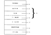
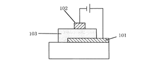
図1に示す本発明の有機EL素子においては、陽極電極層(陽極)1と発光層を含む有機構造体2に挟まれたホ−ル注入層3は、金属酸化物と有機化合物の混合層からなり、前記2種類の物質間で酸化還元反応によってラジカルカチオンとラジカルアニオンからなる電荷移動錯体が形成されていることを特徴としている。つまり、前記混合層中のラジカルカチオン状態(ホ−ル)が電圧印加時に陰極電極層(陰極)方向へ移動することで、ホ−ル注入層として機能することができる。
In the organic EL device of the present invention shown in FIG. 1, a
つまり、本実施形態の有機EL素子において、ホ−ル注入層3は(a)イオン化ポテンシャルが5.7eVより小さく、ホ−ル輸送性すなわち電子供与性を有する有機化合物、及び(b)(a)の有機化合物と酸化還元反応による電荷移動錯体を形成しうる金属酸化物からなる混合層からなり、前記(a)成分と(b)成分との間で酸化還元反応による電荷移動錯体を形成している。
That is, in the organic EL device of this embodiment, the
一般に電子供与性を有する有機化合物が容易にラジカルカチオン状態となるにはイオン化ポテンシャルが5.7eVより小さいことが望ましい。(a)成分の有機化合物のイオン化ポテンシャルが5.7eV以上であると、(b)成分の金属酸化物と酸化還元反応を起こすことが難しくなり、結果的に本発明における電荷移動錯体の形成も困難になる場合がある。 In general, it is desirable that the ionization potential is smaller than 5.7 eV in order for an organic compound having an electron donating property to easily enter a radical cation state. When the ionization potential of the organic compound of component (a) is 5.7 eV or more, it becomes difficult to cause a redox reaction with the metal oxide of component (b), resulting in formation of a charge transfer complex in the present invention. It can be difficult.
さらに具体的には、(a)成分の有機化合物がアリ−ルアミン化合物であり、一般式(I):
このようなアリ−ルアミン化合物の例としては、特に限定はないが、特開平6−25659号公報、特開平6−203963号公報、特開平6−215874号公報、特開平7−145116号公報、特開平7−224012号公報、特開平7−157473号公報、特開平8−48656号公報、特開平7−126226号公報、特開平7−188130号公報、特開平8−40995号公報、特開平8−40996号公報、特開平8−40997号公報、特開平7−126225号公報、特開平7−101911号公報、特開平7−97355号公報に開示されているアリ−ルアミン化合物類が好ましく、例えば、N、N、N’、N’−テトラフェニル−4,4’−ジアミノフェニル、N、N’−ジフェニル−N、N’−ジ(3−メチルフェニル)−4,4’−ジアミノビフェニル、2,2−ビス(4−ジ−p−トリルアミノフェニル)プロパン、N、N、N’、N’−テトラ−p−トリル−4,4’−ジアミノビフェニル、ビス(4−ジ−p−トリルアミノフェニル)フェニルメタン、N,N’−ジフェニル−N,N’−ジ(4−メトキシフェニル)−4,4’−ジアミノビフェニル、N,N,N’,N’−テトラフェニル−4,4’−ジアミノジフェニルエ−テル、4,4’−ビス(ジフェニルアミノ)クオ−ドリフェニル、4−N,N−ジフェニルアミノ−(2−ジフェニルビニル)ベンゼン、3−メトキシ−4’−N,N−ジフェニルアミノスチルベンゼン、N−フェニルカルバゾ−ル、1,1−ビス(4−ジ−p−トリアミノフェニル)−シクロヘキサン、1,1−ビス(4−ジ−p−トリアミノフェニル)−4−フェニルシクロヘキサン、ビス(4−ジメチルアミノ−2−メチルフェニル)−フェニルメタン、N,N,N−トリ(p−トリル)アミン、4−(ジ−p−トリルアミノ)−4’−[4(ジ−p−トリルアミノ)スチリル]スチルベン、N,N,N’,N’−テトラフェニル−4,4’−ジアミノ−ビフェニルN−フェニルカルバゾ−ル、4,4’−ビス[N−(1−ナフチル)−N−フェニル−アミノ]ビフェニル、4,4’’−ビス[N−(1−ナフチル)−N−フェニル−アミノ]p−タ−フェニル、4,4’−ビス[N−(3−アセナフテニル)−N−フェニル−アミノ]ビフェニル、1,5−ビス[N−(1−ナフチル)−N−フェニル−アミノ]ナフタレン、4,4’−ビス[N−(9−アントリル)−N−フェニル−アミノ]ビフェニル、4,4’’−ビス[N−(1−アントリル)−N−フェニル−アミノ]p−タ−フェニル、4,4’−ビス[N−(2−フェナントリル)−N−フェニル−アミノ]ビフェニル、4,4’−ビス[N−(8−フルオランテニル)−N−フェニル−アミノ]ビフェニル、4,4’−ビス[N−(2−ピレニル)−N−フェニル−アミノ]ビフェニル、4,4’−ビス[N−(2−ペリレニル)−N−フェニル−アミノ]ビフェニル、4,4’−ビス[N−(1−コロネニル)−N−フェニル−アミノ]ビフェニル、2,6−ビス(ジ−p−トリルアミノ)ナフタレン、2,6−ビス[ジ−(1−ナフチル)アミノ]ナフタレン、2,6−ビス[N−(1−ナフチル)−N−(2−ナフチル)アミノ]ナフタレン、4.4’’−ビス[N,N−ジ(2−ナフチル)アミノ]タ−フェニル、4.4’−ビス{N−フェニル−N−[4−(1−ナフチル)フェニル]アミノ}ビフェニル、4,4’−ビス[N−フェニル−N−(2−ピレニル)−アミノ]ビフェニル、2,6−ビス[N,N−ジ(2−ナフチル)アミノ]フルオレン、4,4’’−ビス(N,N−ジ−p−トリルアミノ)タ−フェニル、ビス(N−1−ナフチル)(N−2−ナフチル)アミン、下記の式:
またさらに、前記アリ−ルアミン化合物はガラス転移点が90℃以上であるアリ−ルアミン化合物であることが、素子の耐熱性の観点から望ましい。 Furthermore, it is desirable from the viewpoint of the heat resistance of the device that the arylamine compound is an arylamine compound having a glass transition point of 90 ° C. or higher.
上記、化3〜化6に挙げられた化合物はガラス転移点が90℃以上である化合物の好適な例である。
The compounds listed in
また、本実施形態の有機EL素子における陽極電極層に接するホ−ル注入層の最も好適な例は、(a)であるアリ−ルアミン化合物と、(b)前記アリ−ルアミン化合物と酸化還元反応によって電荷移動錯体を形成しうる金属酸化物との混合層がある。 Moreover, the most suitable example of the hole injection layer in contact with the anode electrode layer in the organic EL device of the present embodiment is (a) an arylamine compound, and (b) the arylamine compound and an oxidation-reduction reaction. There is a mixed layer with a metal oxide that can form a charge transfer complex.
さらに、本実施形態のホ−ル注入層を構成する2種類の化合物が酸化還元反応により電荷移動錯体を形成しうるものであるか否かは、吸収スペクトルにより確認できる。吸収スペクトルは、分光学的分析手段(吸収スペクトル測定)によって測定する。本実施形態では、図2に示すように、2種類の化合物が(上述のアリ−ルアミン化合物と金属酸化物)それぞれ単独では、波長800〜2000nmの近赤外領域では吸収スペクトルのピ−クを示さないが、これらの化合物の混合膜では、波長800〜2000nmの近赤外領域に吸収スペクトルのピ−クが顕著に現れている。このため、2種類の化合物間における電子移動を伴う酸化還元反応により、電荷移動錯体が形成されていることが確認できた。
Furthermore, it can be confirmed by an absorption spectrum whether or not two kinds of compounds constituting the hole injection layer of the present embodiment can form a charge transfer complex by an oxidation-reduction reaction. The absorption spectrum is measured by spectroscopic analysis means (absorption spectrum measurement). In the present embodiment, as shown in FIG. 2, when the two kinds of compounds (the above-mentioned arylamine compound and metal oxide) are each alone, the peak of the absorption spectrum is observed in the near infrared region of
図2及び図3に示した各混合膜の吸収スペクトルが、各々の単独の物質の吸収スペクトルの(単純な)重ね合わせではなく、電子移動を伴う反応(つまり酸化還元反応)によって、第3の新たな吸収ピ−クが近赤外線領域800nmから2000nmの位置に観測されており、本発明者らの検討では、前記混合膜中で発生する酸化還元反応の存在が、電圧印加時における電極からの電荷注入を容易にして、結果として素子の駆動電圧を低下させることが判明した。 The absorption spectrum of each mixed film shown in FIGS. 2 and 3 is not a (simple) superposition of the absorption spectra of each single substance, but is caused by a reaction involving electron transfer (that is, a redox reaction). A new absorption peak is observed at a position in the near-infrared region of 800 nm to 2000 nm. According to the study by the present inventors, the presence of the oxidation-reduction reaction occurring in the mixed film is It has been found that charge injection is facilitated, resulting in a reduction in device drive voltage.
本実施形態の有機EL素子は、従来の有機EL素子と同様の成膜順序によって各層を積層してある。すなわち、ガラス基板上に、陽極電極層、ホ−ル注入層、発光層を含む有機構造体、及び陰極電極層が順に積層されている。陰極電極層としての金属やITOは、抵抗加熱蒸着やスパッタリングの手法を用いて成膜することができる。この場合、下記の実施例3に記載されるように、基板上に陽極電極層としてのAlを積層した後、本発明の混合膜をホ−ル注入層として成膜し、最後に透明陰極電極層としてITOを成膜して、成膜面側(ITO側)から光を取り出すトップエミッション構造の素子を実現することができる。一般にAlはホ−ル注入電極としては仕事関数が小さすぎて不向きであると認識されているが、本発明の混合膜をホ−ル注入層として使用すればこのような制限を不問とすることが可能である。 In the organic EL element of this embodiment, the layers are stacked in the same film formation order as that of the conventional organic EL element. That is, an anode electrode layer, a hole injection layer, an organic structure including a light emitting layer, and a cathode electrode layer are sequentially laminated on a glass substrate. The metal or ITO as the cathode electrode layer can be formed using resistance heating vapor deposition or sputtering. In this case, as described in Example 3 below, after laminating Al as the anode electrode layer on the substrate, the mixed film of the present invention was formed as the hole injection layer, and finally the transparent cathode electrode An element having a top emission structure in which ITO is formed as a layer and light is extracted from the film formation surface side (ITO side) can be realized. In general, Al is recognized as being unsuitable for a hole injection electrode because its work function is too small. However, if the mixed film of the present invention is used as a hole injection layer, such a limitation is unquestioned. Is possible.
また逆に、本実施形態の有機EL素子は、従来から広く行われてきた順序とは逆の順序で成膜してある。すわなち、基板上に、陰極電極層、発光層を含む有機構造体、ホ−ル注入層、及び陽極電極層が順に積層されている。陽極電極層としての金属やITOは、ホ−ル注入層を形成した後に、抵抗加熱蒸着やスパッタリングの手法を用いて成膜することができる。この場合は、本発明の(混合層である)ホ−ル注入層が、陽極電極層成膜時、特にスパッタリングプロセスを使用するITO透明電極の成膜プロセス時のダメ−ジ低減層として機能することが期待され、実際、下記実施例5に示すように有効に働くことが示される。 On the contrary, the organic EL element of this embodiment is formed in the reverse order to the order widely performed conventionally. That is, a cathode electrode layer, an organic structure including a light emitting layer, a hole injection layer, and an anode electrode layer are sequentially laminated on the substrate. The metal or ITO as the anode electrode layer can be formed using a resistance heating vapor deposition or sputtering technique after forming the hole injection layer. In this case, the hole injection layer (which is a mixed layer) of the present invention functions as a damage reduction layer during the anode electrode layer deposition, particularly during the ITO transparent electrode deposition process using a sputtering process. In fact, it is shown to work effectively as shown in Example 5 below.
本発明者らは、特願2001−142672号明細書において、有機層にダメ−ジのないスパッタリング成膜の手法を用いて、金属ド−ピングされた電子注入層上に陰極電極層として機能するITO透明導電膜を成膜できることを示している。 In the specification of Japanese Patent Application No. 2001-142672, the inventors function as a cathode electrode layer on a metal-doped electron injection layer by using a sputtering film forming method in which no damage is caused in an organic layer. It shows that an ITO transparent conductive film can be formed.
以下に実施例を挙げて本発明をさらに詳細に説明するが、本発明はこれにより限定されるものではない。 有機化合物、金属酸化物、金属、及びITO透明電極の成膜には、アネルバ製真空蒸着機、またFTSコ−ポレ−ション製スパッタリング装置を使用した。蒸着物質の成膜速度の制御や膜厚の制御は前記蒸着機に取付けられている、水晶振動子を使用した成膜モニタ−CRTM−8000(ULVAC(日本真空技術社)製)を使用した。また、成膜後の実質膜厚の測定には、テンコ−ル(TencOr)社製P10触針式段差計を用いた。素子の特性評価には、ケ−スレ−(KEITHLEY)社ソ−スメ−タ2400、トプコンBM−8輝度計を使用した。素子に直流電圧を0.2V/2秒の割合でステップ状に印加して、電圧上昇1秒後の輝度及び電流値を測定した。また、EL素子のスペクトルは、浜松ホトニクスPMA−11オプチカルマルチチャンネルアナライザ−を使用して定電流駆動し測定した。 The present invention will be described in more detail with reference to examples below, but the present invention is not limited thereto. For the film formation of the organic compound, metal oxide, metal, and ITO transparent electrode, an Anelva vacuum vapor deposition machine or an FTS Corporation sputtering apparatus was used. A film formation monitor-CRTM-8000 (manufactured by ULVAC (Nippon Vacuum Technology Co., Ltd.)) using a crystal resonator, which is attached to the vapor deposition apparatus, was used to control the film formation rate of the vapor deposition material and the film thickness. In addition, a P10 stylus type step meter manufactured by TencOr was used for measurement of the actual film thickness after film formation. For the evaluation of the characteristics of the device, a KETHLEY source meter 2400 and a Topcon BM-8 luminance meter were used. A direct current voltage was applied to the device stepwise at a rate of 0.2 V / 2 seconds, and the luminance and current value after 1 second of voltage increase were measured. The spectrum of the EL element was measured by driving at a constant current using a Hamamatsu Photonics PMA-11 optical multichannel analyzer.
基準例
図4の積層構成を有する従来の有機EL素子を基準例として作製した。ガラス基板11上に陽極透明電極層12として、シ−ト抵抗10Ω/□のITO(インジウム−スズ酸化物、日本板硝子社製)がコ−トされている。その上にホ−ル輸送性(電子供与性)を有する下記式:
次に、前記発光層14の上に、本発明者らが特開平10−270171号公報で開示した電子注入層(金属ド−ピング層、低抵抗電子輸送層)15として、下記式:
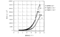
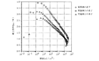
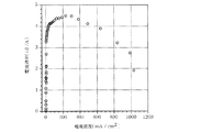
基準例の有機EL素子において、陽極透明電極層12であるITOと陰極電極層16であるAlとの間に、直流電圧を印加し、発光層14(Alq)から緑色発光の輝度を測定した。その結果を図7、図8、図9、図10中の白丸プロット(○)で示す。また、基準例の素子の発光スペクトルを図11の太線で示した。
In the organic EL element of the reference example, a direct current voltage was applied between ITO as the anode
実施例1
図5に実施例1の有機EL素子の積層構造を示す。ガラス基板21上に陽極透明電極層(陽極電極層)22として、シ−ト抵抗10Ω/□のITO(インジウム−スズ酸化物、日本板硝子社製)がコ−トされている。その上に金属酸化物であるV2O5とホ−ル輸送性を有する有機化合物としてのαNPDをモル比率V2O5:αNPD=4:1で共蒸着し、100Åの厚さの混合膜に成膜して、ホ−ル注入層27を形成した。その後は、上記の基準例と同様に、ホ−ル輸送層23であるαNPD、発光層24であるAlq、電子注入層(金属ド−ピング層、低抵抗電子輸送層)25、陰極電極層(陰極)26を順次積層した。なお、ホ−ル輸送層23、発光層24、及び電子注入層25で発光層を含む有機構造体28を構成している。
Example 1
FIG. 5 shows a laminated structure of the organic EL element of Example 1. On the
実施例1の有機EL素子において、陽極透明電極層22であるITOと陰極電極層26であるAlとの間に、直流電圧を印加し、発光層24(Alq)から緑色発光の輝度を測定した。その結果を図7、図8、図9、図10中の白四角プロット(□)で示す。また、実施例1の素子の発光スペクトルを図11の点線で示した。
In the organic EL element of Example 1, a direct current voltage was applied between ITO as the anode
実施例2
図6に実施例2の有機EL素子の積層構造を示す。ガラス基板31上に陽極透明電極層32として、シ−ト抵抗10Ω/□のITO(インジウム−スズ酸化物、日本板硝子社製)がコ−トされている。その上に金属酸化物であるV2O5とホ−ル輸送性を有する有機化合物としてのαNPDをモル比率V2O5:αNPD=4:1で共蒸着し、1000Åの厚さの混合膜に成膜して、本発明のホ−ル注入層37を形成した。その後は、上記の基準例と同様に、ホ−ル輸送層33であるαNPD、発光層34であるAlq、電子注入層(金属ド−ピング層)35、陰極電極層36を順次積層した。なお、ホ−ル輸送層33、発光層34及び電子注入層35で発光層を含む有機構造体38を構成している。 実施例2の有機EL素子において、陽極透明電極層32であるITOと陰極電極層36であるAlとの間に、直流電圧を印加し、発光層34(Alq)から緑色発光の輝度を測定した。その結果を図7、図8、図9、図10中の白三角プロット(△)で示す。また、実施例2の素子の発光スペクトルを図11の細線で示した。
Example 2
FIG. 6 shows a laminated structure of the organic EL element of Example 2. On the
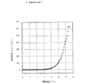
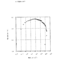
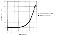
図7〜図11に示すデータに基づいて基準例、実施例1、実施例2の素子を比較すると以下のことが分かった。 (1)実施例1及び実施例2の素子は、実施例1及び実施例2のようなホール注入層を有さない基準例の素子に比べて、駆動電圧が低く(図7)、最高輝度も高い(図8、図10)。
(2)実施例1及び実施例2の素子は、基準例の素子と比較して、高電流密度領域(1000mA/cm2の電流密度単位の領域)でも電流効率(量子効率)の低下がほとんど観測されない(図9)ため、素子の信頼性が高い。
(3)実施例1及び実施例2の素子のように、ホ−ル注入層の膜厚を厚くしても素子の駆動電圧は上昇することがなく、むしろ実施例2のようにホ−ル注入層の膜厚が厚い方が、より低電圧で所望の電流密度を得ることができる(図7)。
(4)発光スペクトルは、前記ホ−ル注入層が1000Åと厚い素子(実施例2)は干渉効果によってピ−ク位置が長波長側にシフトし(図11)、本発明のホ−ル注入層が色調制御にも利用できることが分かった。(実施例2の素子が基準例や実施例1の素子と比べて最高電流効率で若干低い値を示しているのは、この干渉効果によるものである。)
Based on the data shown in FIG. 7 to FIG. 11, the following were found when the elements of the reference example, Example 1 and Example 2 were compared. (1) The device of Example 1 and Example 2 has a lower driving voltage (FIG. 7) and the highest luminance than the device of the reference example that does not have the hole injection layer as in Example 1 and Example 2. (Figs. 8 and 10).
(2) The devices of Examples 1 and 2 have almost no decrease in current efficiency (quantum efficiency) even in the high current density region (region of current density unit of 1000 mA / cm 2 ) compared to the device of the reference example. Since it is not observed (FIG. 9), the reliability of the element is high.
(3) The device driving voltage does not increase even if the thickness of the hole injection layer is increased as in the devices of the first and second embodiments. Rather, as in the second embodiment, the hole is not increased. When the injection layer is thicker, a desired current density can be obtained at a lower voltage (FIG. 7).
(4) The emission spectrum shows that the peak position of the device having the thick hole injection layer as thick as 1000 mm (Example 2) is shifted to the longer wavelength side due to the interference effect (FIG. 11), and the hole injection of the present invention is performed. It was found that the layer can also be used for color control. (The reason why the element of Example 2 shows a slightly lower value in the maximum current efficiency than the element of Reference Example or Example 1 is due to this interference effect.)
実施例3
図12に実施例3のトップエミッション構造有機EL素子の積層構造を示す。ガラス基板41上にAl(アルミニウム、仕事関数4.2eV)を10Å/秒の蒸着速度で1000Åの厚さに成膜して陽極電極層42を形成した。その上に金属酸化物であるV2O5とホ−ル輸送性を有する有機化合物としてのαNPDをモル比率V2O5:αNPD=4:1で共蒸着し、100Åの厚さの混合膜に成膜して、本発明のホ−ル注入層47を形成した。その上にホ−ル輸送層43としてαNPDを10-6Torr(1Torr=133.32Pa)下で、2Å/秒の蒸着速度で600Åの厚さに成膜し、次に発光層44としてAlqをホ−ル輸送層43と同じ条件で600Åの厚さに真空蒸着して形成した。
Example 3
FIG. 12 shows a laminated structure of the top emission structure organic EL element of Example 3. An
次に、前記発光層44の上に、本発明者らが特開平11−233262号公報で開示した電子注入層45を形成するため下記式:
実施例3の有機EL素子において、陽極電極層42であるAlと陰極透明電極層46であるITOとの間に、直流電圧を印加し、発光層44(Alq)から緑色発光の輝度を測定した。その結果を図13、図14、図15、図16中に示す。また、実施例3の素子の発光スペクトルを図17に示した。
In the organic EL device of Example 3, a direct current voltage was applied between Al as the
図14に示すように、実施例3の素子の最高輝度は25000cd/m2を超え、電流効率も基準例や実施例1の素子と比べて遜色ない値が得られた(図15、16)ため、本発明のホ−ル注入層はAlのような低仕事関数金属を陽極電極層として用いても良好に機能することが分かった。 As shown in FIG. 14, the maximum luminance of the element of Example 3 exceeded 25000 cd / m 2 , and the current efficiency was comparable to that of the reference example and Example 1 (FIGS. 15 and 16). Therefore, it was found that the hole injection layer of the present invention functions well even when a low work function metal such as Al is used as the anode electrode layer.
実施例4
図18に実施例4の有機EL素子の積層構造を示す。実施例4の素子は、通常の有機EL素子とは逆の順番に、すなわち、基板上に、陰極透明電極層、発光層を含む有機構造体、ホ−ル注入層、及び陽極電極層が順に積層されている。ガラス基板51上に陰極透明電極層56として、シ−ト抵抗10Ω/□のITO(インジウム−スズ酸化物、日本板硝子社製)がコ−トされている。その上に電子注入層(金属ドーピング層)55として、BCPとCsをモル比率BCP:Cs=4:1で共蒸着し100Åの厚さの混合膜に成膜した。
Example 4
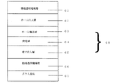
FIG. 18 shows a laminated structure of the organic EL element of Example 4. The element of Example 4 is in the reverse order of the normal organic EL element, that is, on the substrate, the cathode transparent electrode layer, the organic structure including the light emitting layer, the hole injection layer, and the anode electrode layer are sequentially arranged. Are stacked. On the glass substrate 51, ITO (indium-tin oxide, manufactured by Nippon Sheet Glass Co.) having a sheet resistance of 10Ω / □ is coated as the cathode transparent electrode layer 56. On top of that, as an electron injection layer (metal doping layer) 55, BCP and Cs were co-evaporated at a molar ratio BCP: Cs = 4: 1 to form a mixed film having a thickness of 100 mm.
次に、電子注入層55の上に、発光層54として、Alqを600Åの厚さに真空蒸着して形成した。次に発光層54の上にホ−ル輸送層53としてαNPDを600Åの厚さに形成した。その上に金属酸化物であるV2O5とホ−ル輸送性を有する有機化合物としてのαNPDをモル比率V2O5:αNPD=4:1で共蒸着し、100Åの厚さに成膜して、ホ−ル注入層57を形成した。次に、陽極電極層52として、Alを蒸着速度10Å/秒で1000Å(1Å=1×10-10m)蒸着した。発光領域は縦0.2cm、横0.2cmの正方形状とした。なお、ホ−ル輸送層53、発光層54及び電子注入層55で発光層を含む有機構造体58を構成している。 Next, on the electron injection layer 55, the light emitting layer 54 was formed by vacuum deposition of Alq to a thickness of 600 mm. Next, αNPD having a thickness of 600 mm was formed as a hole transport layer 53 on the light emitting layer 54. On top of this, V 2 O 5 which is a metal oxide and αNPD as an organic compound having a hole transporting property are co-deposited at a molar ratio V 2 O 5 : αNPD = 4: 1 to form a film having a thickness of 100 mm. Thus, a hole injection layer 57 was formed. Next, as the anode electrode layer 52, Al was deposited at a rate of 1000 Å (1 Å = 1 × 10 -10 m) at a deposition rate of 10 Å / sec. The light emitting region was a square shape with a length of 0.2 cm and a width of 0.2 cm. The hole transport layer 53, the light emitting layer 54, and the electron injection layer 55 constitute an organic structure 58 including a light emitting layer.
実施例4の有機EL素子において、陰極透明電極層52であるITOと陽極電極層56であるAlとの間に、直流電圧を印加し、発光層54(Alq)から緑色発光の輝度を測定した。その結果を、図19、図20、図21、図22に示す。また、実施例4の素子の発光スペクトルを図23に示した。 In the organic EL device of Example 4, a direct current voltage was applied between ITO as the cathode transparent electrode layer 52 and Al as the anode electrode layer 56, and the luminance of green light emission was measured from the light emitting layer 54 (Alq). . The results are shown in FIG. 19, FIG. 20, FIG. 21, and FIG. The emission spectrum of the device of Example 4 is shown in FIG.
図20に示すように、実施例4の素子の最高輝度は20000cd/m2に達し、電流効率も基準例や実施例1の素子と比べて遜色ない値が得られた(図21、図22)ため、実施例4の有機EL素子は通常の素子と逆順に積層して最後に成膜される陽極電極層の前に、ホ−ル注入層を設けて、かつAlのような低仕事関数金属を陽極電極層として用いても良好に機能することが分かった。 As shown in FIG. 20, the maximum luminance of the element of Example 4 reached 20000 cd / m 2 , and the current efficiency was inferior to that of the reference example and the element of Example 1 (FIGS. 21 and 22). Therefore, the organic EL device of Example 4 is provided with a hole injection layer in front of the anode electrode layer which is laminated in the reverse order to the normal device and is finally formed, and has a low work function such as Al. It has been found that even if metal is used as the anode electrode layer, it functions well.
実施例5
図24に実施例5の有機EL素子の積層構造を示す。実施例5の素子は、通常の有機EL素子とは逆の順番に、すなわち、基板上に、陰極透明電極層、発光層を含む有機構造体、ホ−ル注入層、及び陽極透明電極層が順に積層されている。ガラス基板61上に陰極透明電極層66として、シ−ト抵抗10Ω/□のITO(インジウム−スズ酸化物、日本板硝子社製)がコ−トされている。その上に電子注入層65として、BCPとCsをモル比率BCP:Cs=4:1で共蒸着し100Åの厚さの混合膜に成膜した。
Example 5
FIG. 24 shows the laminated structure of the organic EL element of Example 5. The element of Example 5 is in the reverse order of a normal organic EL element, that is, an organic structure including a cathode transparent electrode layer, a light emitting layer, a hole injection layer, and an anode transparent electrode layer on a substrate. They are stacked in order. On the glass substrate 61, ITO (indium-tin oxide, manufactured by Nippon Sheet Glass Co., Ltd.) having a sheet resistance of 10Ω / □ is coated as the cathode transparent electrode layer 66. On top of that, as an electron injection layer 65, BCP and Cs were co-evaporated at a molar ratio BCP: Cs = 4: 1 to form a mixed film having a thickness of 100 mm.
次に、電子注入層65の上に、発光層64としてAlqを600Åの厚さに真空蒸着して形成した。次に発光層64の上にホ−ル輸送層63としてαNPDを600Åの厚さに形成した。その上に金属酸化物であるV2O5とホ−ル輸送性を有する有機化合物としてのαNPDとをモル比率V2O5:αNPD=4:1で共蒸着し、1000Åの厚さに成膜して、ホ−ル注入層67を形成した。なお、ホ−ル輸送層63、発光層64及び電子注入層65で発光層を含む有機構造体68を構成している。次に、陽極透明電極層(陽極層)62として、ITOをスパッタリングの手法で成膜速度4Å/秒で1000Å蒸着した。発光領域は縦0.2cm、横0.2cmの正方形状とした。
Next, Alq was vacuum deposited on the electron injection layer 65 as a
実施例5の有機EL素子において、陰極透明電極層66であるITOと陽極透明電極層62であるITOとの間に、直流電圧を印加し、発光層64(Alq)から緑色発光の輝度を測定した。その結果を図25、図26、図27、図28に示す。これらの図において、ガラス基板(基板)側からの測定結果を白丸プロット(○)で、成膜面側から見た測定結果を黒丸プロット(●)で示した。また、図29において、実施例5の素子のガラス基板(基板)側から見た発光スペクトルを実線で、成膜面側から見た発光スペクトルを図29の点線で示した。
In the organic EL element of Example 5, a direct current voltage was applied between ITO as the cathode transparent electrode layer 66 and ITO as the anode
実施例5の素子は、ガラス基板側と成膜面側(陽極透明電極層側)のいずれからも発光を観察できる透明な発光素子である。しかし、両発光スペクトルは図29に示すように、干渉効果により互いに異なるものであった。 The element of Example 5 is a transparent light emitting element capable of observing light emission from both the glass substrate side and the film formation surface side (anode transparent electrode layer side). However, both emission spectra were different from each other due to the interference effect as shown in FIG.
また、実施例5の素子は通常の素子と逆順に積層しており、最後に成膜される陽極電極層の前にホ−ル注入層を設けている。このため、陽極透明電極層62であるITOのスパッタリングプロセスのような高エネルギ−粒子を含むプロセスにおいても、ホール注入層67によって保護されることにより、発光層を含む有機構造体68へのダメ−ジが低減され、ホール注入層67がダメージ低減層として良好に機能することが分かった。
The element of Example 5 is laminated in the reverse order of the normal element, and a hole injection layer is provided in front of the anode electrode layer to be finally formed. For this reason, even in a process including high energy particles such as a sputtering process of ITO, which is the anode
なお、本実施形態にかかる有機エレクトロルミネッセント素子は、複数の発光ユニット(陰極電極層と陽極電極層に挟まれた層部分、例えば、「(陽極)/ホール注入層/ホール輸送層/発光層/電子注入層/(陰極)」という構成の素子の場合は、「ホール注入層/ホール輸送層/発光層/電子注入層」が「発光ユニット」に相当する。)が電荷発生層によって仕切られた構造を採用してもよく、電圧印加時には電荷発生層がホ−ル発生層と電子発生層として機能して、結果的に複数の有機EL素子が直列に接続されたように同時に発光させることができる。電荷発生層は、その陰極電極層側に接する発光ユニットに対してはホ−ル注入層として機能し、またその陽極電極層側に接する発光ユニットに対しては電子注入層として機能しうる。 The organic electroluminescent device according to this embodiment includes a plurality of light emitting units (layer portions sandwiched between a cathode electrode layer and an anode electrode layer, for example, “(anode) / hole injection layer / hole transport layer / light emission). In the case of an element having a structure of “layer / electron injection layer / (cathode)”, “hole injection layer / hole transport layer / light emitting layer / electron injection layer” corresponds to “light emitting unit”). The charge generation layer functions as a hole generation layer and an electron generation layer when a voltage is applied, and as a result, a plurality of organic EL elements are caused to emit light simultaneously as if they are connected in series. be able to. The charge generation layer can function as a hole injection layer for the light emitting unit in contact with the cathode electrode layer side, and can function as an electron injection layer for the light emitting unit in contact with the anode electrode layer side.
参考例
参考例として、本発明のホール注入層の比抵抗(Ω・cm)を、被測定物の比抵抗の値(レンジ)によって2種類の方法で測定した。
Reference Example As a reference example, the specific resistance (Ω · cm) of the hole injection layer of the present invention was measured by two methods according to the specific resistance value (range) of the object to be measured.
第1の測定法(サンドイッチ法)は、比較的比抵抗の大きい物質に対して適当とされる方法で、被測定物の蒸着薄膜を電極で狭持した形態(図30及び図31に示すサンドイッチ構造の比抵抗評価用素子)で測定を行った。印加電圧(V)と被測定物薄膜の膜厚(cm)(つまり電極間距離)から得られる電場E(V/cm)及び観測電流(A)と電流が流れる領域の断面積(cm2)とから得られる電流密度(A/cm2)の比〔(V/cm)/(A/cm2)=(Ω・cm)〕として比抵抗を算出した。 The first measurement method (sandwich method) is a method suitable for a substance having a relatively large specific resistance, and is a configuration in which a vapor-deposited thin film of an object to be measured is held between electrodes (a sandwich shown in FIGS. 30 and 31). Measurement was performed with a specific resistance evaluation element of the structure. The electric field E (V / cm) obtained from the applied voltage (V) and the film thickness (cm) (that is, the distance between the electrodes) of the thin film to be measured, and the cross-sectional area (cm 2 ) of the observation current (A) and the current flow region. The specific resistance was calculated as the ratio of current density (A / cm 2 ) obtained from the above ([V / cm) / (A / cm 2 ) = (Ω · cm)].
具体的には(2mm幅の)ITO電極101上に(場合により2mm幅のAl電極上に)被測定物103を所望の膜厚になるように蒸着し、最後に(同じく2mm幅の)アルミニウム電極102をITO電極101と直交するように成膜して、比抵抗評価用素子を作製した。
Specifically, the object to be measured 103 is vapor-deposited on the ITO electrode 101 (2 mm width) (optionally on a 2 mm width Al electrode) to a desired film thickness, and finally aluminum (also 2 mm width) is finally formed. The
第2の測定法(並置法)は、比較的比抵抗の小さい物質に対して適当とされる方法で、並置構造の比抵抗評価用素子を用いて測定する。すなわち、図32及び図33に示したように、基板200上の同一平面上に予め陽極電極層201、陰極電極層202となる電極を所定距離(Lcm)隔てて成膜されたものを用意しておき、その上から被測定物203の蒸着薄膜を所定の開口幅(Wcm)を有するエリア規定用金属マスクを介して、所定の膜厚(tcm)を成膜する。この場合得られる電場E(V/cm)は、印加電圧(V)を電極間距離(Lcm)で除して算出され、電流密度(A/cm2)は観測電流(A)を電流が流れる領域の断面積(この場合はW×tcm2)で除して算出される。このようにして得られた値から、前記のサンドイッチ構造の場合と同様に、比抵抗(Ω・cm)を算出した。
The second measurement method (a juxtaposition method) is a method suitable for a substance having a relatively small specific resistance, and is measured using a specific resistance evaluation element having a juxtaposed structure. That is, as shown in FIG. 32 and FIG. 33, an electrode in which electrodes to be the
被測定物は、ITO(透明電極材料)、V2O5、V2O5とαNPDの共蒸着膜(V2O5:αNPD=4:1、1:1、1:2の3種類のモル比)、V2O5と2−TNATAの共蒸着膜〔V2O5:2−TNATA=4:1(モル比)〕、CsとBCPの共蒸着膜〔Cs:BCP=1:1(モル比)、実施例中の電子注入層〕〕、α−NPD、Alq3である。ITO、V2O5とαNPDの共蒸着膜、及びV2O5と2−TNATAの共蒸着膜については、並置構造の比抵抗評価用素子で測定し、CsとBCPの共蒸着膜、α−NPD及びAlq3については、サンドイッチ構造の比抵抗評価用素子で測定した。さらにα−NPDついては電極からの電荷注入をオ−ミック(ohmic)にするため、本発明のホ−ル注入層の組成である、V2O5とαNPDの混合膜を両電極に接する部分に50Åと薄く形成した上で、1000Åの厚さのαNPDをサンドイッチして測定した。また、V2O5については、並置構造とサンドイッチ構造の両方で測定し、測定法によらず略同一の比抵抗が得られることを確認した。 The object to be measured is co-deposited film of ITO (transparent electrode material), V 2 O 5 , V 2 O 5 and αNPD (V 2 O 5 : αNPD = 4: 1, 1: 1, 1: 2). Molar ratio), V 2 O 5 and 2-TNATA co-deposited film [V 2 O 5 : 2-TNATA = 4: 1 (molar ratio)], Cs and BCP co-deposited film [Cs: BCP = 1: 1 (Molar ratio, electron injection layer in examples)], α-NPD, Alq 3 . The co-deposited film of ITO, V 2 O 5 and αNPD, and the co-deposited film of V 2 O 5 and 2-TNATA were measured with an element for evaluating resistivity of a juxtaposed structure, and co-deposited film of Cs and BCP, α for -NPD and Alq 3, it was measured with a resistivity evaluation device of the sandwich structure. Furthermore, for α-NPD, in order to make charge injection from the electrodes ohmic, the mixed film of V 2 O 5 and αNPD, which is the composition of the hole injection layer of the present invention, is formed in the portion in contact with both electrodes. After thinly forming 50 mm, αNPD having a thickness of 1000 mm was sandwiched and measured. As for the V 2 O 5, it was measured both juxtaposed structures and sandwich structure was confirmed that substantially the same specific resistance is obtained regardless of the measuring method.
図34から算出した比抵抗は以下のとおりである。
(1)並置法で測定
−○− ITO 4.6×10⁻⁴Ω・cm
−●− V2O5 7.2×10⁴Ω・cm
−▲− (V2O5:αNPD=4:1)の共蒸着膜 2.0×10³Ω・cm
−◇− (V2O5:αNPD=1:1)の共蒸着膜 3.6×10⁴Ω・cm
−+− (V2O5:αNPD=1:2)の共蒸着膜 2.9×10⁵Ω・cm
−□− (V2O5:2−TNATA=4:1)の共蒸着膜 5.8×10³Ω・cm
The specific resistance calculated from FIG. 34 is as follows.
(1) Measured by juxtaposition method-○-ITO 4.6 × 10 −4 Ω · cm
− ● − V 2 O 5 7.2 × 10 4 Ω · cm
− ▲ − (V 2 O 5 : αNPD = 4: 1) co-deposited film 2.0 × 10 3 Ω · cm
-◇-Co-deposited film of (V 2 O 5 : αNPD = 1: 1) 3.6 × 10 4 Ω · cm
-+-(V 2 O 5 : αNPD = 1: 2) co-deposited film 2.9 × 10 5 Ω · cm
-□-(V 2 O 5 : 2-TNATA = 4: 1) co-deposited film 5.8 × 10 3 Ω · cm
(2)サンドイッチ法で測定
−△− ITO/V2O5/Al 2.8×10⁵Ω・cm
−☆− ITO/Cs:BCP/Al 1.7×10⁵Ω・cm
−▼− Al/Alq3/Al 4.8×10¹³Ω・cm
−★− ITO/αNPD/Al 1.5×10¹³Ω・cm
−■− ITO/V2O5:αNPD(50Å)/αNPD(1000Å)/V2O5:αNPD(50Å)/Al 8.0×10⁸Ω・cm
この結果に示すように、V2O5を含むホール注入層の比抵抗は、1.0×10²Ω・cm以上かつ1.0×10¹⁰Ω・cm未満の範囲内にある。
(2) Measurement by sandwich method -Δ- ITO / V 2 O 5 / Al 2.8 × 10 5 Ω · cm
-☆-ITO / Cs: BCP / Al 1.7 × 10 5 Ω · cm
-▼-Al / Alq 3 / Al 4.8 × 10 13 Ω · cm
-★-ITO / αNPD / Al 1.5 × 10 13 Ω · cm
-■-ITO / V 2 O 5 : αNPD (50 Å) / αNPD (1000 Å) / V 2 O 5 : αNPD (50 Å) / Al 8.0 × 10 8 Ω · cm
As shown in this result, the specific resistance of the hole injection layer containing V 2 O 5 is in the range of 1.0 × 10 2 Ω · cm or more and less than 1.0 × 10 10 Ω · cm.
図35に示されるとおり、本実施形態の金属酸化物と有機化合物の混合膜であるホ−ル注入層は、両物質の混合によりそれぞれの物質が単独では示すことのない低い比抵抗を示し、この事実によっても電子移動に伴う酸化還元反応の存在が示唆されており、ひいては素子の低駆動電圧化と高効率化にこのホ−ル注入層が有効である基礎的な証明となっている。 As shown in FIG. 35, the hole injection layer which is a mixed film of a metal oxide and an organic compound according to the present embodiment exhibits a low specific resistance that cannot be exhibited by each material alone by mixing both materials, This fact also suggests the existence of a redox reaction associated with electron transfer, which in turn is a basic proof that this hole injection layer is effective in reducing the drive voltage and efficiency of the device.
なお、本実施形態のホ−ル注入層の膜厚は、特に制限はないが5Å以上とすることが好ましい。このホ−ル注入層中では無電場の状態でもアリ−ルアミン化合物がラジカルカチオンの状態で存在し、内部電荷として振る舞えるので膜厚には特に上限はなく、その低い比抵抗値の故に厚膜にしても素子の電圧上昇をもたらすことがないので電極間の距離を通常の有機EL素子の場合よりも長く設定することにより短絡の危険性を大幅に軽減する手段としても有用である。したがって電極間の総膜厚を2000Å以上にしても、通常の有機EL素子と変わらない低電圧駆動が可能である。 The film thickness of the hole injection layer of this embodiment is not particularly limited, but is preferably 5 mm or more. In this hole injection layer, the arylamine compound exists in the state of radical cation even in the absence of an electric field and can act as an internal charge, so there is no particular upper limit to the film thickness, and because of its low specific resistance value, a thick film However, since the voltage of the element is not increased, it is useful as a means for greatly reducing the risk of short circuit by setting the distance between the electrodes longer than that in the case of a normal organic EL element. Therefore, even when the total film thickness between the electrodes is 2000 mm or more, low voltage driving that is the same as that of a normal organic EL element is possible.
1、42、52 陽極電極層
2、28、38、48、58、68 発光層を含む有機構造体
3、27、37、47、57、67 ホ−ル注入層
21、31、41、51、61 ガラス基板
22、32、62 陽極電極層(陽極透明電極層)
23、33、43、53、63 ホール輸送層
24、34、44、54、64 発光層
25、35、45、55、65 電子注入層
26、36 陰極電極層(陰極層)
46、56、66 陰極電極層(陰極透明電極層)
1, 42, 52
23, 33, 43, 53, 63
46, 56, 66 Cathode electrode layer (cathode transparent electrode layer)
Claims (18)
前記ホ−ル注入層は金属酸化物と有機化合物がモル分率4:1の混合膜を含み、前記混合膜は共蒸着によって形成されており、前記混合膜中の前記有機化合物は、イオン化ポテンシャルが5.7eVより小さく、ホ−ル輸送性を有し、前記混合膜は、前記金属酸化物と前記有機化合物間との酸化還元反応によって生成した前記有機化合物のラジカルカチオンと前記金属酸化物のラジカルアニオンからなる電荷移動錯体を有し、前記電荷移動錯体中の前記ラジカルカチオンが、電圧印加時に前記陰極電極層の方向へ移動することにより、前記発光層へホ−ルが注入されることを特徴とする有機エレクトロルミネッセント素子。 An anode electrode layer, a cathode electrode layer disposed opposite to the anode electrode layer, a hole injection layer in contact with the anode electrode layer, located between the anode electrode layer and the cathode electrode layer, An organic electroluminescent device having at least one light emitting layer, wherein at least one of the anode electrode layer and the cathode electrode layer is transparent,
The hole injection layer includes a mixed film of a metal oxide and an organic compound in a molar ratio of 4: 1 , the mixed film is formed by co-evaporation, and the organic compound in the mixed film has an ionization potential. Is less than 5.7 eV, and has a hole transport property, and the mixed film includes a radical cation of the organic compound generated by an oxidation-reduction reaction between the metal oxide and the organic compound, and the metal oxide. A charge transfer complex comprising a radical anion, wherein the radical cation in the charge transfer complex moves toward the cathode electrode layer when a voltage is applied, whereby holes are injected into the light emitting layer. An organic electroluminescent device characterized.
Priority Applications (7)
| Application Number | Priority Date | Filing Date | Title |
|---|---|---|---|
| JP2003358402A JP4476594B2 (en) | 2003-10-17 | 2003-10-17 | Organic electroluminescent device |
| CNB2004100805030A CN100466331C (en) | 2003-10-17 | 2004-09-30 | Organic electroluminescent device |
| TW093130520A TWI367048B (en) | 2003-10-17 | 2004-10-08 | Organic electroluminescent device |
| KR1020040082844A KR100894306B1 (en) | 2003-10-17 | 2004-10-15 | Organic electroluminescent device |
| US10/966,251 US8558451B2 (en) | 2003-10-17 | 2004-10-15 | Organic electroluminescent device |
| ES04024610.0T ES2636486T3 (en) | 2003-10-17 | 2004-10-15 | Procedure to produce an organic electroluminescent device |
| EP04024610.0A EP1524706B1 (en) | 2003-10-17 | 2004-10-15 | Method for producing an organic electroluminescent device |
Applications Claiming Priority (1)
| Application Number | Priority Date | Filing Date | Title |
|---|---|---|---|
| JP2003358402A JP4476594B2 (en) | 2003-10-17 | 2003-10-17 | Organic electroluminescent device |
Related Child Applications (1)
| Application Number | Title | Priority Date | Filing Date |
|---|---|---|---|
| JP2009258054A Division JP4926229B2 (en) | 2009-11-11 | 2009-11-11 | Organic electroluminescent device |
Publications (3)
| Publication Number | Publication Date |
|---|---|
| JP2005123095A JP2005123095A (en) | 2005-05-12 |
| JP2005123095A5 JP2005123095A5 (en) | 2006-04-27 |
| JP4476594B2 true JP4476594B2 (en) | 2010-06-09 |
Family
ID=34373644
Family Applications (1)
| Application Number | Title | Priority Date | Filing Date |
|---|---|---|---|
| JP2003358402A Expired - Lifetime JP4476594B2 (en) | 2003-10-17 | 2003-10-17 | Organic electroluminescent device |
Country Status (7)
| Country | Link |
|---|---|
| US (1) | US8558451B2 (en) |
| EP (1) | EP1524706B1 (en) |
| JP (1) | JP4476594B2 (en) |
| KR (1) | KR100894306B1 (en) |
| CN (1) | CN100466331C (en) |
| ES (1) | ES2636486T3 (en) |
| TW (1) | TWI367048B (en) |
Cited By (1)
| Publication number | Priority date | Publication date | Assignee | Title |
|---|---|---|---|---|
| KR20160114950A (en) | 2015-03-25 | 2016-10-06 | (주)부흥산업사 | Novel aromatic triazine derivatives for organic electroluminescent device and their preparation intermediates |
Families Citing this family (126)
| Publication number | Priority date | Publication date | Assignee | Title |
|---|---|---|---|---|
| JPWO2005002010A1 (en) * | 2003-06-27 | 2006-08-10 | 株式会社半導体エネルギー研究所 | Organic laser equipment |
| US20050008052A1 (en) * | 2003-07-01 | 2005-01-13 | Ryoji Nomura | Light-emitting device |
| EP1776846B1 (en) | 2003-09-26 | 2013-04-10 | Semiconductor Energy Laboratory Co., Ltd. | Light-emitting device and method for manufacturing the same |
| US7605534B2 (en) * | 2003-12-02 | 2009-10-20 | Semiconductor Energy Laboratory Co., Ltd. | Light-emitting element having metal oxide and light-emitting device using the same |
| CN101673808B (en) | 2003-12-26 | 2012-05-23 | 株式会社半导体能源研究所 | Light-emitting element |
| KR101187402B1 (en) * | 2004-05-21 | 2012-10-02 | 가부시키가이샤 한도오따이 에네루기 켄큐쇼 | Lighting appliance |
| JP4925569B2 (en) * | 2004-07-08 | 2012-04-25 | ローム株式会社 | Organic electroluminescent device |
| JP2006295104A (en) | 2004-07-23 | 2006-10-26 | Semiconductor Energy Lab Co Ltd | Light emitting element and light emitting device using the same |
| EP1624502B1 (en) * | 2004-08-04 | 2015-11-18 | Semiconductor Energy Laboratory Co., Ltd. | Light-emitting element, display device, and electronic appliance |
| KR101251622B1 (en) | 2004-09-24 | 2013-04-08 | 가부시키가이샤 한도오따이 에네루기 켄큐쇼 | Light emitting device |
| US7737626B2 (en) * | 2004-09-30 | 2010-06-15 | Semiconductor Energy Laboratory Co., Ltd. | Light emitting element |
| KR101436791B1 (en) | 2004-10-29 | 2014-09-03 | 가부시키가이샤 한도오따이 에네루기 켄큐쇼 | Composite material, light-emitting element, light-emitting device, and manufacturing method thereof |
| US7683532B2 (en) * | 2004-11-02 | 2010-03-23 | Semiconductor Energy Laboratory Co., Ltd. | Semiconductor device and light emitting device |
| WO2006059736A1 (en) * | 2004-11-30 | 2006-06-08 | Semiconductor Energy Laboratory Co., Ltd. | Light emitting element, light emitting device, and electronic device |
| CN101847690B (en) | 2004-11-30 | 2012-08-08 | 株式会社半导体能源研究所 | Light emitting element and light emitting device |
| CN101116197B (en) * | 2004-12-06 | 2010-05-12 | 株式会社半导体能源研究所 | Composite material comprising organic compound and inorganic compound, light emitting element and light emitting device employing the composite material as well as manufacturing method of the light em |
| EP1820218A4 (en) * | 2004-12-06 | 2010-03-24 | Semiconductor Energy Lab | Organic field-effect transistor and semiconductor device including the same |
| JP2006164708A (en) | 2004-12-06 | 2006-06-22 | Semiconductor Energy Lab Co Ltd | Electronic equipment and light-emitting device |
| JP4789598B2 (en) * | 2004-12-06 | 2011-10-12 | 株式会社半導体エネルギー研究所 | LIGHT EMITTING ELEMENT AND ELECTRONIC DEVICE |
| CN101073164B (en) * | 2004-12-06 | 2010-05-05 | 株式会社半导体能源研究所 | Light-emitting element and light-emitting device using the same |
| US7989694B2 (en) | 2004-12-06 | 2011-08-02 | Semiconductor Energy Laboratory Co., Ltd. | Photoelectric conversion element, solar battery, and photo sensor |
| JP2006190995A (en) * | 2004-12-06 | 2006-07-20 | Semiconductor Energy Lab Co Ltd | Composite material comprising organic compound and inorganic compound, light emitting element and light emitting device employing the composite material as well as manufacturing method of the light emitting element |
| US7919772B2 (en) * | 2004-12-14 | 2011-04-05 | Semiconductor Energy Laboratory Co., Ltd. | Semiconductor device and manufacturing method thereof |
| WO2006070913A1 (en) * | 2004-12-28 | 2006-07-06 | Semiconductor Energy Laboratory Co., Ltd. | Light emitting element |
| US20080154005A1 (en) * | 2005-01-31 | 2008-06-26 | Semiconductor Energy Laboratory Co., Ltd. | Hole-Injecting Material, Material for Light-Emitting Element, Light-Emitting Element, Organic Compound, Monomer, and Monomer Mixture |
| JP5159042B2 (en) * | 2005-02-08 | 2013-03-06 | 株式会社半導体エネルギー研究所 | LIGHT EMITTING ELEMENT, LIGHT EMITTING DEVICE, AND ELECTRONIC DEVICE |
| KR101272098B1 (en) | 2005-02-08 | 2013-06-07 | 가부시키가이샤 한도오따이 에네루기 켄큐쇼 | Light-emitting element, light-emitting device, and electronic appliance |
| US9530968B2 (en) | 2005-02-15 | 2016-12-27 | Semiconductor Energy Laboratory Co., Ltd. | Light emitting element and light emitting device |
| JP5707013B2 (en) * | 2005-02-28 | 2015-04-22 | 株式会社半導体エネルギー研究所 | COMPOSITE MATERIAL, AND LIGHT EMITTING ELEMENT, LIGHT EMITTING DEVICE, AND ELECTRIC DEVICE USING THE COMPOSITE MATERIAL |
| EP1866983A4 (en) * | 2005-02-28 | 2009-10-21 | Semiconductor Energy Lab | Composite material, light emitting element, light emitting device and electronic appliance using the composite material |
| US7626198B2 (en) | 2005-03-22 | 2009-12-01 | Semiconductor Energy Laboratory Co., Ltd. | Nonlinear element, element substrate including the nonlinear element, and display device |
| WO2006101016A1 (en) | 2005-03-23 | 2006-09-28 | Semiconductor Energy Laboratory Co., Ltd. | Composite material, light emitting element and light emitting device |
| US7649197B2 (en) | 2005-03-23 | 2010-01-19 | Semiconductor Energy Laboratory Co., Ltd. | Composite material, and light emitting element and light emitting device using the composite material |
| US7977865B2 (en) * | 2005-03-23 | 2011-07-12 | Semiconductor Energy Laboratory Co., Ltd. | Composite material, material for light-emitting element, light-emitting element, light-emitting device and electronic device |
| US7851989B2 (en) | 2005-03-25 | 2010-12-14 | Semiconductor Energy Laboratory Co., Ltd. | Light emitting device |
| JP5072243B2 (en) * | 2005-03-25 | 2012-11-14 | 株式会社半導体エネルギー研究所 | Light emitting device |
| US7777232B2 (en) * | 2005-04-11 | 2010-08-17 | Semiconductor Energy Laboratory Co., Ltd. | Display device and electronic device using the same |
| WO2006109878A1 (en) | 2005-04-11 | 2006-10-19 | Semiconductor Energy Laboratory Co., Ltd. | Light-emitting element, light-emitting device, and vapor deposition apparatus |
| JP5314834B2 (en) * | 2005-04-21 | 2013-10-16 | 株式会社半導体エネルギー研究所 | LIGHT EMITTING ELEMENT, LIGHT EMITTING DEVICE, LIGHTING DEVICE, AND ELECTRONIC DEVICE |
| CN101853923B (en) * | 2005-04-21 | 2013-05-22 | 株式会社半导体能源研究所 | Light emitting element, light emitting device, and electronic device |
| US8049208B2 (en) * | 2005-04-22 | 2011-11-01 | Semiconductor Energy Laboratory Co., Ltd. | Organic semiconductor device having composite electrode |
| US7745019B2 (en) * | 2005-04-28 | 2010-06-29 | Semiconductor Energy Laboratory Co., Ltd. | Light emitting element and light emitting device and method of manufacturing light emitting element |
| US20060250078A1 (en) * | 2005-05-09 | 2006-11-09 | City University Of Hong Kong | Organic electroluminescent devices incorporating UV-illuminated fluorocarbon layers |
| JP2006324537A (en) * | 2005-05-20 | 2006-11-30 | Hitachi Displays Ltd | Display device |
| JP4596976B2 (en) * | 2005-05-20 | 2010-12-15 | 株式会社 日立ディスプレイズ | Organic light emitting display |
| EP1724852A3 (en) * | 2005-05-20 | 2010-01-27 | Semiconductor Energy Laboratory Co., Ltd. | Light emitting element, light emitting device, and electronic device |
| JP5116992B2 (en) * | 2005-05-27 | 2013-01-09 | 富士フイルム株式会社 | Organic EL device |
| US7687986B2 (en) | 2005-05-27 | 2010-03-30 | Fujifilm Corporation | Organic EL device having hole-injection layer doped with metallic oxide |
| US8334057B2 (en) | 2005-06-08 | 2012-12-18 | Semiconductor Energy Laboratory Co., Ltd. | Light-emitting element, light-emitting device, and electronic device |
| JP2006344774A (en) * | 2005-06-09 | 2006-12-21 | Rohm Co Ltd | Organic el device, organic el display using the same, and method of manufacturing organic el device |
| JP2007019487A (en) * | 2005-06-09 | 2007-01-25 | Semiconductor Energy Lab Co Ltd | Light emitting device and electronic device |
| US8269227B2 (en) | 2005-06-09 | 2012-09-18 | Semiconductor Energy Laboratory Co., Ltd. | Light emitting device and electronic device |
| JP5554922B2 (en) * | 2005-06-10 | 2014-07-23 | トムソン ライセンシング | Organic light-emitting diode with two or less layers of different organic materials |
| JP5072271B2 (en) * | 2005-06-22 | 2012-11-14 | 株式会社半導体エネルギー研究所 | LIGHT EMITTING DEVICE AND ELECTRONIC DEVICE USING THE SAME |
| US8017252B2 (en) | 2005-06-22 | 2011-09-13 | Semiconductor Energy Laboratory Co., Ltd. | Light emitting device and electronic appliance using the same |
| US8729795B2 (en) | 2005-06-30 | 2014-05-20 | Semiconductor Energy Laboratory Co., Ltd. | Light emitting device and electronic device |
| JP5132092B2 (en) * | 2005-06-30 | 2013-01-30 | 株式会社半導体エネルギー研究所 | Method for manufacturing light emitting device |
| US7745989B2 (en) | 2005-06-30 | 2010-06-29 | Semiconductor Energy Laboratory Co., Ltd | Light emitting element, light emitting device, and electronic apparatus |
| JP4890117B2 (en) * | 2005-06-30 | 2012-03-07 | 株式会社半導体エネルギー研究所 | Light emitting device and manufacturing method thereof |
| US8288180B2 (en) | 2005-07-04 | 2012-10-16 | Semiconductor Energy Laboratory Co., Ltd. | Method for manufacturing light emitting device |
| US8415878B2 (en) * | 2005-07-06 | 2013-04-09 | Semiconductor Energy Laboratory Co., Ltd. | Light-emitting element, light-emitting device, and electronic device |
| US8659008B2 (en) | 2005-07-08 | 2014-02-25 | Semiconductor Energy Laboratory Co., Ltd. | Composite material and light emitting element, light emitting device, and electronic device using the composite material |
| JP4954623B2 (en) * | 2005-07-08 | 2012-06-20 | 株式会社半導体エネルギー研究所 | Light emitting device |
| WO2007013478A1 (en) | 2005-07-25 | 2007-02-01 | Semiconductor Energy Laboratory Co., Ltd. | Light-emitting element, light-emitting device, and electronic appliance |
| KR101288588B1 (en) * | 2005-08-12 | 2013-07-22 | 가부시키가이샤 한도오따이 에네루기 켄큐쇼 | Arylamine compound and synthetic method thereof |
| KR20130121997A (en) | 2005-09-12 | 2013-11-06 | 가부시키가이샤 한도오따이 에네루기 켄큐쇼 | Quinoxaline derivative, and light emitting element, light emitting device, and electronic appliance using the same |
| US20070108894A1 (en) * | 2005-11-17 | 2007-05-17 | Idemitsu Kosan Co., Ltd. | Organic electroluminescent device |
| JP5078329B2 (en) * | 2005-11-30 | 2012-11-21 | 株式会社半導体エネルギー研究所 | LIGHT EMITTING ELEMENT, LIGHT EMITTING DEVICE, AND ELECTRONIC DEVICE |
| JP2007227907A (en) * | 2006-01-26 | 2007-09-06 | Semiconductor Energy Lab Co Ltd | Organic field effect transistor and semiconductor device |
| WO2007086534A1 (en) | 2006-01-26 | 2007-08-02 | Semiconductor Energy Laboratory Co., Ltd. | Organic field effect transistor and semiconductor device |
| EP1821579A3 (en) * | 2006-02-17 | 2008-04-02 | Semiconductor Energy Laboratory Co., Ltd. | Light emitting element, light emitting device, and electronic appliance |
| US20070194321A1 (en) * | 2006-02-17 | 2007-08-23 | Semiconductor Energy Laboratory Co., Ltd. | Light emitting element, light emitting device, and electronic device |
| TWI277367B (en) * | 2006-03-03 | 2007-03-21 | Au Optronics Corp | Hole injection structure of organic electroluminescence device and method for manufacturing the same |
| WO2007102704A1 (en) * | 2006-03-07 | 2007-09-13 | Lg Chem, Ltd. | Oled and fabricating method of the same |
| CN101400757B (en) * | 2006-03-14 | 2013-05-15 | Lg化学株式会社 | Organic light emitting diode having high efficiency and process for fabricating the same |
| US20070215889A1 (en) * | 2006-03-20 | 2007-09-20 | Semiconductor Energy Laboratory Co., Ltd. | Aromatic amine compound, and light-emitting element, light-emitting device, and electronic appliance using the aromatic amine compound |
| US9112170B2 (en) | 2006-03-21 | 2015-08-18 | Semiconductor Energy Laboratory Co., Ltd. | Light-emitting element, light-emitting device, and electronic device |
| JP2008034367A (en) * | 2006-07-04 | 2008-02-14 | Semiconductor Energy Lab Co Ltd | Display device |
| US8974918B2 (en) * | 2006-07-04 | 2015-03-10 | Semiconductor Energy Laboratory Co., Ltd. | Display device and electronic device |
| JP2008112904A (en) * | 2006-10-31 | 2008-05-15 | Idemitsu Kosan Co Ltd | Organic electroluminescent element |
| US20080111131A1 (en) * | 2006-11-10 | 2008-05-15 | Nam-Choul Yang | Organic thin film transistor, method of fabricating the same, and display device including the same |
| TW200824497A (en) * | 2006-11-21 | 2008-06-01 | Au Optronics Corp | Organic electro-luminescent device |
| CN1976087B (en) * | 2006-12-04 | 2010-09-08 | 友达光电股份有限公司 | Organic electroluminescent device |
| WO2008069259A1 (en) * | 2006-12-05 | 2008-06-12 | Semiconductor Energy Laboratory Co., Ltd. | Film formation apparatus, film formation method, manufacturing apparatus, and method for manufacturing light-emitting device |
| WO2008075615A1 (en) | 2006-12-21 | 2008-06-26 | Semiconductor Energy Laboratory Co., Ltd. | Light-emitting element and light-emitting device |
| WO2008108254A1 (en) * | 2007-03-07 | 2008-09-12 | Semiconductor Energy Laboratory Co., Ltd. | Light-emitting element and light-emitting device |
| CN101271869B (en) * | 2007-03-22 | 2015-11-25 | 株式会社半导体能源研究所 | The manufacture method of luminescent device |
| JP2008251626A (en) * | 2007-03-29 | 2008-10-16 | Kyocera Corp | Organic electroluminescence element, manufacturing process of organic electroluminescence element and organic electroluminescence display |
| EP1986473B1 (en) * | 2007-04-03 | 2017-01-25 | Tsinghua University | Organic electroluminescent device |
| US7875881B2 (en) * | 2007-04-03 | 2011-01-25 | Semiconductor Energy Laboratory Co., Ltd. | Memory device and semiconductor device |
| KR101482760B1 (en) | 2007-06-14 | 2015-01-15 | 가부시키가이샤 한도오따이 에네루기 켄큐쇼 | Light-emitting device, electronic device, and manufacturing method of light-emitting device |
| US8093806B2 (en) | 2007-06-20 | 2012-01-10 | Semiconductor Energy Laboratory Co., Ltd. | Light-emitting device, method for manufacturing the same, and electronic apparatus |
| JP5208591B2 (en) | 2007-06-28 | 2013-06-12 | 株式会社半導体エネルギー研究所 | Light emitting device and lighting device |
| KR102022839B1 (en) * | 2007-12-03 | 2019-09-20 | 가부시키가이샤 한도오따이 에네루기 켄큐쇼 | Carbazole derivative, and light-emitting element, light-emitting device, and electronic device using carbazole derivative |
| EP2075850A3 (en) * | 2007-12-28 | 2011-08-24 | Semiconductor Energy Laboratory Co, Ltd. | Photoelectric conversion device and manufacturing method thereof |
| KR101003232B1 (en) * | 2008-01-23 | 2010-12-21 | 주식회사 엘지화학 | Organic electroluminescent device and method for fabricating the same |
| JP2010153365A (en) | 2008-11-19 | 2010-07-08 | Semiconductor Energy Lab Co Ltd | Light-emitting element, light-emitting device, electronic equipment, and illumination device |
| JP5717944B2 (en) * | 2008-11-21 | 2015-05-13 | ユー・ディー・シー アイルランド リミテッド | Organic electroluminescent device and manufacturing method thereof |
| KR101707430B1 (en) * | 2009-05-29 | 2017-02-16 | 가부시키가이샤 한도오따이 에네루기 켄큐쇼 | Light-emitting element, light-emitting device, lighting device, and electronic appliance |
| US9741955B2 (en) * | 2009-05-29 | 2017-08-22 | Semiconductor Energy Laboratory Co., Ltd. | Light-emitting element, light-emitting device, and method for manufacturing the same |
| KR101691395B1 (en) * | 2009-09-04 | 2017-01-02 | 가부시키가이샤 한도오따이 에네루기 켄큐쇼 | Light-emitting element, light-emitting device, and method for manufacturing the same |
| DE102009047883A1 (en) * | 2009-09-30 | 2011-03-31 | Osram Opto Semiconductors Gmbh | Opto-electronic organic component and method for its production |
| US8404500B2 (en) | 2009-11-02 | 2013-03-26 | Semiconductor Energy Laboratory Co., Ltd. | Method for manufacturing light-emitting element, light-emitting element, light-emitting device, lighting device, and electronic appliance |
| JP2011139044A (en) | 2009-12-01 | 2011-07-14 | Semiconductor Energy Lab Co Ltd | Luminous element, luminous device, electronic equipment, and lighting device |
| CN103154187B (en) | 2010-10-04 | 2015-06-17 | 株式会社半导体能源研究所 | Composite material, light-emitting element, light-emitting device, electronic device, and lighting device |
| JP5969216B2 (en) | 2011-02-11 | 2016-08-17 | 株式会社半導体エネルギー研究所 | Light emitting element, display device, lighting device, and manufacturing method thereof |
| KR101894898B1 (en) * | 2011-02-11 | 2018-09-04 | 가부시키가이샤 한도오따이 에네루기 켄큐쇼 | Light-emitting device and electronic device using light-emitting device |
| JP2012182443A (en) | 2011-02-11 | 2012-09-20 | Semiconductor Energy Lab Co Ltd | Light-emitting element and light-emitting device |
| US20120234392A1 (en) * | 2011-03-17 | 2012-09-20 | Semiconductor Energy Laboratory Co., Ltd. | Photoelectric conversion device |
| EP2503618B1 (en) | 2011-03-23 | 2014-01-01 | Semiconductor Energy Laboratory Co., Ltd. | Composite material, light-emitting element, light-emitting device, electronic device, and lighting device |
| KR101960759B1 (en) * | 2011-04-08 | 2019-03-21 | 가부시키가이샤 한도오따이 에네루기 켄큐쇼 | Light-emitting device, electronic appliance, and lighting device |
| TWI602334B (en) | 2011-05-13 | 2017-10-11 | 半導體能源研究所股份有限公司 | Light-emitting element and light-emitting device |
| US9419239B2 (en) * | 2011-07-08 | 2016-08-16 | Semiconductor Energy Laboratory Co., Ltd. | Composite material, light-emitting element, light-emitting device, electronic device, lighting device, and organic compound |
| US9159939B2 (en) | 2011-07-21 | 2015-10-13 | Semiconductor Energy Laboratory Co., Ltd. | Photoelectric conversion device |
| JP2013058562A (en) | 2011-09-07 | 2013-03-28 | Semiconductor Energy Lab Co Ltd | Photoelectric conversion device |
| US9136478B2 (en) * | 2011-10-14 | 2015-09-15 | Lg Display Co., Ltd. | Organic light emitting device and display panel using the same method, terminal, and server for implementing fast playout |
| DE102012200084B4 (en) | 2012-01-04 | 2021-05-12 | Pictiva Displays International Limited | RADIATION-EMITTING ORGANIC COMPONENT |
| JP5892924B2 (en) * | 2012-12-28 | 2016-03-23 | エルジー ディスプレイ カンパニー リミテッド | Organic EL device, method for manufacturing organic EL device, and organic EL display |
| CN104051632A (en) * | 2013-03-11 | 2014-09-17 | 海洋王照明科技股份有限公司 | Organic light-emitting device and preparation method thereof |
| JP6174877B2 (en) | 2013-03-21 | 2017-08-02 | 株式会社半導体エネルギー研究所 | Display device and electronic device |
| JP6114592B2 (en) | 2013-03-21 | 2017-04-12 | 株式会社半導体エネルギー研究所 | Display device, manufacturing method thereof, and electronic apparatus |
| PL2978845T3 (en) * | 2013-03-27 | 2020-11-16 | Isarna Therapeutics Gmbh | Modified tgf-beta oligonucleotides |
| CN103500801B (en) * | 2013-10-12 | 2016-08-24 | 上海和辉光电有限公司 | The luminous blue light organic emissive diode in top and manufacture method thereof |
| KR102377360B1 (en) | 2014-08-08 | 2022-03-21 | 가부시키가이샤 한도오따이 에네루기 켄큐쇼 | Light-emitting element, light-emitting device, lighting device, display device, display panel, and electronic appliance |
| US11917840B2 (en) | 2018-05-18 | 2024-02-27 | Semiconductor Energy Laboratory Co., Ltd. | Light-emitting device with reflective electrode and light-emitting layer |
| US11903232B2 (en) | 2019-03-07 | 2024-02-13 | Semiconductor Energy Laboratory Co., Ltd. | Light-emitting device comprising charge-generation layer between light-emitting units |
Family Cites Families (71)
| Publication number | Priority date | Publication date | Assignee | Title |
|---|---|---|---|---|
| US4356429A (en) | 1980-07-17 | 1982-10-26 | Eastman Kodak Company | Organic electroluminescent cell |
| US4539507A (en) | 1983-03-25 | 1985-09-03 | Eastman Kodak Company | Organic electroluminescent devices having improved power conversion efficiencies |
| US5089862A (en) * | 1986-05-12 | 1992-02-18 | Warner Jr Raymond M | Monocrystalline three-dimensional integrated circuit |
| US4847749A (en) * | 1986-06-13 | 1989-07-11 | International Business Machines Corporation | Job interrupt at predetermined boundary for enhanced recovery |
| US4720432A (en) | 1987-02-11 | 1988-01-19 | Eastman Kodak Company | Electroluminescent device with organic luminescent medium |
| US4885211A (en) | 1987-02-11 | 1989-12-05 | Eastman Kodak Company | Electroluminescent device with improved cathode |
| JPS6449771A (en) | 1987-08-20 | 1989-02-27 | Mitsubishi Electric Corp | Mechanical seal |
| US5218672A (en) * | 1990-01-19 | 1993-06-08 | Sony Corporation Of America | Offline editing system with user interface for controlling edit list generation |
| US5059862A (en) | 1990-07-26 | 1991-10-22 | Eastman Kodak Company | Electroluminescent device with improved cathode |
| JPH0625659A (en) | 1992-07-07 | 1994-02-01 | Idemitsu Kosan Co Ltd | Phosphamine derivative, its preparation, and electroluminescent element made using the same |
| WO1994014115A2 (en) * | 1992-12-01 | 1994-06-23 | Microsoft Corporation | A method and system for in-place interaction with embedded objects |
| JPH06203963A (en) | 1993-01-08 | 1994-07-22 | Idemitsu Kosan Co Ltd | Organic electroluminescent element |
| JPH06215874A (en) | 1993-01-20 | 1994-08-05 | Idemitsu Kosan Co Ltd | Organic electroluminescent element |
| JP3419534B2 (en) | 1993-02-10 | 2003-06-23 | 靖彦 城田 | Trisarylaminobenzene derivative, compound for organic EL device and organic EL device |
| JP3549555B2 (en) | 1993-10-04 | 2004-08-04 | 株式会社リコー | Novel pyrene derivative and method for producing the same |
| JP3220950B2 (en) | 1993-11-01 | 2001-10-22 | 保土谷化学工業株式会社 | Benzidine compound |
| JP3574860B2 (en) | 1993-11-01 | 2004-10-06 | 保土谷化学工業株式会社 | Tetraphenylbenzidine compound |
| JPH07145116A (en) | 1993-11-25 | 1995-06-06 | Nisshinbo Ind Inc | Aromatic diamine compound |
| JPH07157473A (en) | 1993-12-06 | 1995-06-20 | Chisso Corp | Triazine derivative, its production and electric field luminescent element using the same |
| JP3594642B2 (en) | 1993-12-24 | 2004-12-02 | 保土谷化学工業株式会社 | Diaminodiphenyl compound and organic electroluminescent device using the compound |
| JP3579746B2 (en) | 1994-02-07 | 2004-10-20 | チッソ株式会社 | Diphenylamine derivative |
| JP3828595B2 (en) | 1994-02-08 | 2006-10-04 | Tdk株式会社 | Organic EL device |
| JP3593719B2 (en) | 1994-08-04 | 2004-11-24 | 東洋インキ製造株式会社 | Novel triphenylamine derivative, its production method and use |
| JP3593717B2 (en) | 1994-08-04 | 2004-11-24 | 東洋インキ製造株式会社 | Novel triphenylamine derivative, its production method and use |
| JP3593718B2 (en) | 1994-08-04 | 2004-11-24 | 東洋インキ製造株式会社 | Novel triphenylamine derivative, its production method and use |
| US5862372A (en) * | 1994-11-16 | 1999-01-19 | Morris; Robert M. | Visually oriented computer implemented application development system utilizing standardized objects and multiple views |
| JPH08278957A (en) * | 1995-04-04 | 1996-10-22 | Fujitsu Ltd | Analysis support device for unexecutable solution and infinite solution |
| JP2824411B2 (en) * | 1995-08-25 | 1998-11-11 | 株式会社豊田中央研究所 | Organic thin-film light emitting device |
| US6195142B1 (en) * | 1995-12-28 | 2001-02-27 | Matsushita Electrical Industrial Company, Ltd. | Organic electroluminescence element, its manufacturing method, and display device using organic electroluminescence element |
| WO1997029426A1 (en) * | 1996-02-09 | 1997-08-14 | Sony Corporation | Information processor, file name changing method and recording medium on which file name changing program is stored |
| JPH10270171A (en) | 1997-01-27 | 1998-10-09 | Junji Kido | Organic electroluminescent element |
| US5956481A (en) * | 1997-02-06 | 1999-09-21 | Microsoft Corporation | Method and apparatus for protecting data files on a computer from virus infection |
| US5925980A (en) * | 1997-05-01 | 1999-07-20 | Motorola, Inc. | Organic electroluminescent device with graded region |
| US6658417B1 (en) * | 1997-12-31 | 2003-12-02 | International Business Machines Corporation | Term-based methods and apparatus for access to files on shared storage devices |
| JP4514841B2 (en) | 1998-02-17 | 2010-07-28 | 淳二 城戸 | Organic electroluminescent device |
| JPH11251067A (en) | 1998-03-02 | 1999-09-17 | Junji Kido | Organic electroluminescence element |
| US6442755B1 (en) * | 1998-07-07 | 2002-08-27 | United Video Properties, Inc. | Electronic program guide using markup language |
| JP4069505B2 (en) * | 1998-07-27 | 2008-04-02 | チッソ株式会社 | Trinaphthylbenzene derivative and organic electroluminescence device using the same |
| JP3978757B2 (en) | 1998-08-05 | 2007-09-19 | 株式会社ジーエス・ユアサコーポレーション | Gas diffusion electrode-electrolyte membrane assembly for fuel cell and method for producing the same |
| US6487566B1 (en) * | 1998-10-05 | 2002-11-26 | International Business Machines Corporation | Transforming documents using pattern matching and a replacement language |
| US6192367B1 (en) * | 1998-11-23 | 2001-02-20 | International Business Machines Corporation | Data file editor presenting semi-formatted view |
| CA2255017A1 (en) * | 1998-11-30 | 2000-05-30 | Christina P. Lau | Method and mechanism for a task oriented xml data model |
| JP4505067B2 (en) | 1998-12-16 | 2010-07-14 | 淳二 城戸 | Organic electroluminescent device |
| JP3440991B2 (en) * | 1999-03-05 | 2003-08-25 | 日本電気株式会社 | File revision management system |
| US6476828B1 (en) * | 1999-05-28 | 2002-11-05 | International Business Machines Corporation | Systems, methods and computer program products for building and displaying dynamic graphical user interfaces |
| US7086002B2 (en) * | 1999-09-27 | 2006-08-01 | International Business Machines Corporation | System and method for creating and editing, an on-line publication |
| JP4824848B2 (en) | 2000-02-29 | 2011-11-30 | 淳二 城戸 | Organic electroluminescent device, organic electroluminescent device group, and method for identifying emission spectrum thereof |
| TW474114B (en) | 1999-09-29 | 2002-01-21 | Junji Kido | Organic electroluminescent device, organic electroluminescent device assembly and method of controlling the emission spectrum in the device |
| US6549922B1 (en) * | 1999-10-01 | 2003-04-15 | Alok Srivastava | System for collecting, transforming and managing media metadata |
| JP2001142627A (en) | 1999-11-15 | 2001-05-25 | Brother Ind Ltd | Coordinate reader |
| KR100377321B1 (en) * | 1999-12-31 | 2003-03-26 | 주식회사 엘지화학 | Electronic device comprising organic compound having p-type semiconducting characteristics |
| US20040205473A1 (en) * | 2000-01-27 | 2004-10-14 | Gwyn Fisher | Method and system for implementing an enterprise information portal |
| US6760723B2 (en) * | 2000-01-31 | 2004-07-06 | Commvault Systems Inc. | Storage management across multiple time zones |
| US6874130B1 (en) * | 2000-02-17 | 2005-03-29 | International Business Machines Corporation | Copy/move graphical user interface apparatus and method |
| US6901403B1 (en) * | 2000-03-02 | 2005-05-31 | Quovadx, Inc. | XML presentation of general-purpose data sources |
| JP4617019B2 (en) * | 2000-04-25 | 2011-01-19 | 大日本印刷株式会社 | EL device having photocatalyst containing layer and method for producing the same |
| US6654737B1 (en) * | 2000-05-23 | 2003-11-25 | Centor Software Corp. | Hypertext-based database architecture |
| JP4076769B2 (en) * | 2000-12-28 | 2008-04-16 | 株式会社半導体エネルギー研究所 | Light emitting device and electric appliance |
| US6968505B2 (en) * | 2001-04-27 | 2005-11-22 | International Business Machines Corporation | Use of conceptual diagrams to support relationships between launchpads and its wizards |
| JP3955744B2 (en) | 2001-05-14 | 2007-08-08 | 淳二 城戸 | Manufacturing method of organic thin film element |
| JP4154869B2 (en) * | 2001-06-21 | 2008-09-24 | 株式会社豊田中央研究所 | Organic electroluminescence device |
| JP3825395B2 (en) * | 2001-10-30 | 2006-09-27 | 株式会社半導体エネルギー研究所 | Light emitting device and electric appliance |
| US7146564B2 (en) * | 2001-12-21 | 2006-12-05 | Xmlcities, Inc. | Extensible stylesheet designs using meta-tag and/or associated meta-tag information |
| US7188160B2 (en) * | 2002-01-22 | 2007-03-06 | Ericsson Ab | Method and apparatus for updating network device configuration information in a network management system |
| JP4032783B2 (en) * | 2002-03-15 | 2008-01-16 | 株式会社デンソー | Organic EL device |
| JP3933591B2 (en) * | 2002-03-26 | 2007-06-20 | 淳二 城戸 | Organic electroluminescent device |
| US7490167B2 (en) * | 2002-05-22 | 2009-02-10 | Sony Corporation | System and method for platform and language-independent development and delivery of page-based content |
| US7143344B2 (en) * | 2002-06-12 | 2006-11-28 | Microsoft Corporation | Transformation stylesheet editor |
| CA2414479A1 (en) * | 2002-12-16 | 2004-06-16 | Ibm Canada Limited - Ibm Canada Limitee | A visual debugger for stylesheets |
| EP1776846B1 (en) * | 2003-09-26 | 2013-04-10 | Semiconductor Energy Laboratory Co., Ltd. | Light-emitting device and method for manufacturing the same |
| US7441011B2 (en) * | 2003-10-23 | 2008-10-21 | Microsoft Corporation | Truth on client persistent caching |
-
2003
- 2003-10-17 JP JP2003358402A patent/JP4476594B2/en not_active Expired - Lifetime
-
2004
- 2004-09-30 CN CNB2004100805030A patent/CN100466331C/en active Active
- 2004-10-08 TW TW093130520A patent/TWI367048B/en active
- 2004-10-15 KR KR1020040082844A patent/KR100894306B1/en active IP Right Grant
- 2004-10-15 ES ES04024610.0T patent/ES2636486T3/en active Active
- 2004-10-15 US US10/966,251 patent/US8558451B2/en active Active
- 2004-10-15 EP EP04024610.0A patent/EP1524706B1/en active Active
Cited By (1)
| Publication number | Priority date | Publication date | Assignee | Title |
|---|---|---|---|---|
| KR20160114950A (en) | 2015-03-25 | 2016-10-06 | (주)부흥산업사 | Novel aromatic triazine derivatives for organic electroluminescent device and their preparation intermediates |
Also Published As
| Publication number | Publication date |
|---|---|
| KR100894306B1 (en) | 2009-04-24 |
| ES2636486T3 (en) | 2017-10-05 |
| EP1524706A3 (en) | 2006-05-10 |
| CN100466331C (en) | 2009-03-04 |
| US8558451B2 (en) | 2013-10-15 |
| TW200524477A (en) | 2005-07-16 |
| US20050084712A1 (en) | 2005-04-21 |
| KR20050037390A (en) | 2005-04-21 |
| CN1610470A (en) | 2005-04-27 |
| EP1524706B1 (en) | 2017-05-03 |
| EP1524706A2 (en) | 2005-04-20 |
| TWI367048B (en) | 2012-06-21 |
| JP2005123095A (en) | 2005-05-12 |
Similar Documents
| Publication | Publication Date | Title |
|---|---|---|
| JP4476594B2 (en) | Organic electroluminescent device | |
| US10312474B2 (en) | Organic electroluminescent device comprising a plurality of light emissive units | |
| JP4683829B2 (en) | Organic electroluminescent device and manufacturing method thereof | |
| JP4300176B2 (en) | Organic electroluminescent device | |
| US9466799B2 (en) | Organic devices, organic electroluminescent devices and organic solar cells | |
| JP4926229B2 (en) | Organic electroluminescent device |
Legal Events
| Date | Code | Title | Description |
|---|---|---|---|
| A711 | Notification of change in applicant |
Free format text: JAPANESE INTERMEDIATE CODE: A711 Effective date: 20051128 |
|
| A521 | Request for written amendment filed |
Free format text: JAPANESE INTERMEDIATE CODE: A523 Effective date: 20060119 |
|
| A521 | Request for written amendment filed |
Free format text: JAPANESE INTERMEDIATE CODE: A523 Effective date: 20060310 |
|
| A621 | Written request for application examination |
Free format text: JAPANESE INTERMEDIATE CODE: A621 Effective date: 20060310 |
|
| RD04 | Notification of resignation of power of attorney |
Free format text: JAPANESE INTERMEDIATE CODE: A7424 Effective date: 20071226 |
|
| A711 | Notification of change in applicant |
Free format text: JAPANESE INTERMEDIATE CODE: A711 Effective date: 20080605 |
|
| A521 | Request for written amendment filed |
Free format text: JAPANESE INTERMEDIATE CODE: A821 Effective date: 20080605 |
|
| A977 | Report on retrieval |
Free format text: JAPANESE INTERMEDIATE CODE: A971007 Effective date: 20090402 |
|
| A131 | Notification of reasons for refusal |
Free format text: JAPANESE INTERMEDIATE CODE: A131 Effective date: 20090421 |
|
| A521 | Request for written amendment filed |
Free format text: JAPANESE INTERMEDIATE CODE: A523 Effective date: 20090617 |
|
| A02 | Decision of refusal |
Free format text: JAPANESE INTERMEDIATE CODE: A02 Effective date: 20090811 |
|
| A521 | Request for written amendment filed |
Free format text: JAPANESE INTERMEDIATE CODE: A523 Effective date: 20091111 |
|
| A911 | Transfer to examiner for re-examination before appeal (zenchi) |
Free format text: JAPANESE INTERMEDIATE CODE: A911 Effective date: 20091119 |
|
| TRDD | Decision of grant or rejection written | ||
| A01 | Written decision to grant a patent or to grant a registration (utility model) |
Free format text: JAPANESE INTERMEDIATE CODE: A01 Effective date: 20100209 |
|
| A01 | Written decision to grant a patent or to grant a registration (utility model) |
Free format text: JAPANESE INTERMEDIATE CODE: A01 |
|
| A61 | First payment of annual fees (during grant procedure) |
Free format text: JAPANESE INTERMEDIATE CODE: A61 Effective date: 20100310 |
|
| R150 | Certificate of patent or registration of utility model |
Ref document number: 4476594 Country of ref document: JP Free format text: JAPANESE INTERMEDIATE CODE: R150 Free format text: JAPANESE INTERMEDIATE CODE: R150 |
|
| FPAY | Renewal fee payment (event date is renewal date of database) |
Free format text: PAYMENT UNTIL: 20130319 Year of fee payment: 3 |
|
| FPAY | Renewal fee payment (event date is renewal date of database) |
Free format text: PAYMENT UNTIL: 20140319 Year of fee payment: 4 |
|
| R250 | Receipt of annual fees |
Free format text: JAPANESE INTERMEDIATE CODE: R250 |
|
| R250 | Receipt of annual fees |
Free format text: JAPANESE INTERMEDIATE CODE: R250 |
|
| R250 | Receipt of annual fees |
Free format text: JAPANESE INTERMEDIATE CODE: R250 |
|
| R250 | Receipt of annual fees |
Free format text: JAPANESE INTERMEDIATE CODE: R250 |
|
| R250 | Receipt of annual fees |
Free format text: JAPANESE INTERMEDIATE CODE: R250 |
|
| R250 | Receipt of annual fees |
Free format text: JAPANESE INTERMEDIATE CODE: R250 |
|
| R250 | Receipt of annual fees |
Free format text: JAPANESE INTERMEDIATE CODE: R250 |
|
| S531 | Written request for registration of change of domicile |
Free format text: JAPANESE INTERMEDIATE CODE: R313531 |
|
| R350 | Written notification of registration of transfer |
Free format text: JAPANESE INTERMEDIATE CODE: R350 |
|
| RD03 | Notification of appointment of power of attorney |
Free format text: JAPANESE INTERMEDIATE CODE: R3D03 |
|
| R250 | Receipt of annual fees |
Free format text: JAPANESE INTERMEDIATE CODE: R250 |
|
| R250 | Receipt of annual fees |
Free format text: JAPANESE INTERMEDIATE CODE: R250 |
|
| R250 | Receipt of annual fees |
Free format text: JAPANESE INTERMEDIATE CODE: R250 |
|
| R250 | Receipt of annual fees |
Free format text: JAPANESE INTERMEDIATE CODE: R250 |
|
| EXPY | Cancellation because of completion of term |