JP5969216B2 - Light emitting element, display device, lighting device, and manufacturing method thereof - Google Patents
Light emitting element, display device, lighting device, and manufacturing method thereof Download PDFInfo
- Publication number
- JP5969216B2 JP5969216B2 JP2012023596A JP2012023596A JP5969216B2 JP 5969216 B2 JP5969216 B2 JP 5969216B2 JP 2012023596 A JP2012023596 A JP 2012023596A JP 2012023596 A JP2012023596 A JP 2012023596A JP 5969216 B2 JP5969216 B2 JP 5969216B2
- Authority
- JP
- Japan
- Prior art keywords
- layer
- light
- electrode
- light emitting
- conductive layer
- Prior art date
- Legal status (The legal status is an assumption and is not a legal conclusion. Google has not performed a legal analysis and makes no representation as to the accuracy of the status listed.)
- Expired - Fee Related
Links
- 238000004519 manufacturing process Methods 0.000 title claims description 17
- 239000000463 material Substances 0.000 claims description 96
- 239000004065 semiconductor Substances 0.000 claims description 43
- 238000000034 method Methods 0.000 claims description 27
- 229910044991 metal oxide Inorganic materials 0.000 claims description 20
- 150000004706 metal oxides Chemical class 0.000 claims description 20
- RTAQQCXQSZGOHL-UHFFFAOYSA-N Titanium Chemical compound [Ti] RTAQQCXQSZGOHL-UHFFFAOYSA-N 0.000 claims description 17
- 239000010936 titanium Substances 0.000 claims description 17
- 229910052719 titanium Inorganic materials 0.000 claims description 17
- 230000005669 field effect Effects 0.000 claims description 13
- 238000010438 heat treatment Methods 0.000 claims description 9
- 230000001747 exhibiting effect Effects 0.000 claims description 8
- 229910021332 silicide Inorganic materials 0.000 claims 4
- -1 ITO) Inorganic materials 0.000 description 39
- 230000006870 function Effects 0.000 description 34
- 239000000758 substrate Substances 0.000 description 34
- 238000002347 injection Methods 0.000 description 33
- 239000007924 injection Substances 0.000 description 33
- 239000012535 impurity Substances 0.000 description 28
- 239000000126 substance Substances 0.000 description 27
- 239000003990 capacitor Substances 0.000 description 26
- 229910052757 nitrogen Inorganic materials 0.000 description 25
- 230000005525 hole transport Effects 0.000 description 17
- CUJRVFIICFDLGR-UHFFFAOYSA-N acetylacetonate Chemical compound CC(=O)[CH-]C(C)=O CUJRVFIICFDLGR-UHFFFAOYSA-N 0.000 description 16
- 150000001875 compounds Chemical class 0.000 description 14
- 239000002131 composite material Substances 0.000 description 13
- XAGFODPZIPBFFR-UHFFFAOYSA-N aluminium Chemical compound [Al] XAGFODPZIPBFFR-UHFFFAOYSA-N 0.000 description 12
- 229910052782 aluminium Inorganic materials 0.000 description 11
- AZFHXIBNMPIGOD-UHFFFAOYSA-N 4-hydroxypent-3-en-2-one iridium Chemical compound [Ir].CC(O)=CC(C)=O.CC(O)=CC(C)=O.CC(O)=CC(C)=O AZFHXIBNMPIGOD-UHFFFAOYSA-N 0.000 description 10
- XUIMIQQOPSSXEZ-UHFFFAOYSA-N Silicon Chemical compound [Si] XUIMIQQOPSSXEZ-UHFFFAOYSA-N 0.000 description 10
- 229910052799 carbon Inorganic materials 0.000 description 10
- 238000010586 diagram Methods 0.000 description 10
- 229910052710 silicon Inorganic materials 0.000 description 10
- 239000010703 silicon Substances 0.000 description 10
- 239000002585 base Substances 0.000 description 9
- MILUBEOXRNEUHS-UHFFFAOYSA-N iridium(3+) Chemical compound [Ir+3] MILUBEOXRNEUHS-UHFFFAOYSA-N 0.000 description 9
- 229910052814 silicon oxide Inorganic materials 0.000 description 9
- VYPSYNLAJGMNEJ-UHFFFAOYSA-N Silicium dioxide Chemical compound O=[Si]=O VYPSYNLAJGMNEJ-UHFFFAOYSA-N 0.000 description 8
- 239000007983 Tris buffer Substances 0.000 description 8
- 238000005401 electroluminescence Methods 0.000 description 8
- 150000002894 organic compounds Chemical class 0.000 description 8
- 238000004544 sputter deposition Methods 0.000 description 8
- 125000005595 acetylacetonate group Chemical group 0.000 description 7
- 230000015572 biosynthetic process Effects 0.000 description 7
- 239000003086 colorant Substances 0.000 description 7
- 239000011159 matrix material Substances 0.000 description 7
- IJGRMHOSHXDMSA-UHFFFAOYSA-N Atomic nitrogen Chemical compound N#N IJGRMHOSHXDMSA-UHFFFAOYSA-N 0.000 description 6
- 229910006404 SnO 2 Inorganic materials 0.000 description 6
- XLOMVQKBTHCTTD-UHFFFAOYSA-N Zinc monoxide Chemical compound [Zn]=O XLOMVQKBTHCTTD-UHFFFAOYSA-N 0.000 description 6
- ZUOUZKKEUPVFJK-UHFFFAOYSA-N diphenyl Chemical compound C1=CC=CC=C1C1=CC=CC=C1 ZUOUZKKEUPVFJK-UHFFFAOYSA-N 0.000 description 6
- 229910052751 metal Inorganic materials 0.000 description 6
- 239000002184 metal Substances 0.000 description 6
- 229910000476 molybdenum oxide Inorganic materials 0.000 description 6
- 229920000642 polymer Polymers 0.000 description 6
- 239000011521 glass Substances 0.000 description 5
- 239000011777 magnesium Substances 0.000 description 5
- 125000001997 phenyl group Chemical group [H]C1=C([H])C([H])=C(*)C([H])=C1[H] 0.000 description 5
- 238000003860 storage Methods 0.000 description 5
- IYZMXHQDXZKNCY-UHFFFAOYSA-N 1-n,1-n-diphenyl-4-n,4-n-bis[4-(n-phenylanilino)phenyl]benzene-1,4-diamine Chemical compound C1=CC=CC=C1N(C=1C=CC(=CC=1)N(C=1C=CC(=CC=1)N(C=1C=CC=CC=1)C=1C=CC=CC=1)C=1C=CC(=CC=1)N(C=1C=CC=CC=1)C=1C=CC=CC=1)C1=CC=CC=C1 IYZMXHQDXZKNCY-UHFFFAOYSA-N 0.000 description 4
- UOCMXZLNHQBBOS-UHFFFAOYSA-N 2-(1,3-benzoxazol-2-yl)phenol zinc Chemical compound [Zn].Oc1ccccc1-c1nc2ccccc2o1.Oc1ccccc1-c1nc2ccccc2o1 UOCMXZLNHQBBOS-UHFFFAOYSA-N 0.000 description 4
- FQJQNLKWTRGIEB-UHFFFAOYSA-N 2-(4-tert-butylphenyl)-5-[3-[5-(4-tert-butylphenyl)-1,3,4-oxadiazol-2-yl]phenyl]-1,3,4-oxadiazole Chemical compound C1=CC(C(C)(C)C)=CC=C1C1=NN=C(C=2C=C(C=CC=2)C=2OC(=NN=2)C=2C=CC(=CC=2)C(C)(C)C)O1 FQJQNLKWTRGIEB-UHFFFAOYSA-N 0.000 description 4
- ZVFQEOPUXVPSLB-UHFFFAOYSA-N 3-(4-tert-butylphenyl)-4-phenyl-5-(4-phenylphenyl)-1,2,4-triazole Chemical compound C1=CC(C(C)(C)C)=CC=C1C(N1C=2C=CC=CC=2)=NN=C1C1=CC=C(C=2C=CC=CC=2)C=C1 ZVFQEOPUXVPSLB-UHFFFAOYSA-N 0.000 description 4
- DHDHJYNTEFLIHY-UHFFFAOYSA-N 4,7-diphenyl-1,10-phenanthroline Chemical compound C1=CC=CC=C1C1=CC=NC2=C1C=CC1=C(C=3C=CC=CC=3)C=CN=C21 DHDHJYNTEFLIHY-UHFFFAOYSA-N 0.000 description 4
- 102100040577 Dermatan-sulfate epimerase-like protein Human genes 0.000 description 4
- 101000816741 Homo sapiens Dermatan-sulfate epimerase-like protein Proteins 0.000 description 4
- FYYHWMGAXLPEAU-UHFFFAOYSA-N Magnesium Chemical compound [Mg] FYYHWMGAXLPEAU-UHFFFAOYSA-N 0.000 description 4
- AZWHFTKIBIQKCA-UHFFFAOYSA-N [Sn+2]=O.[O-2].[In+3] Chemical compound [Sn+2]=O.[O-2].[In+3] AZWHFTKIBIQKCA-UHFFFAOYSA-N 0.000 description 4
- MWPLVEDNUUSJAV-UHFFFAOYSA-N anthracene Chemical compound C1=CC=CC2=CC3=CC=CC=C3C=C21 MWPLVEDNUUSJAV-UHFFFAOYSA-N 0.000 description 4
- 239000004305 biphenyl Substances 0.000 description 4
- 238000010549 co-Evaporation Methods 0.000 description 4
- 238000004040 coloring Methods 0.000 description 4
- AMWRITDGCCNYAT-UHFFFAOYSA-L hydroxy(oxo)manganese;manganese Chemical compound [Mn].O[Mn]=O.O[Mn]=O AMWRITDGCCNYAT-UHFFFAOYSA-L 0.000 description 4
- 230000003287 optical effect Effects 0.000 description 4
- PQQKPALAQIIWST-UHFFFAOYSA-N oxomolybdenum Chemical compound [Mo]=O PQQKPALAQIIWST-UHFFFAOYSA-N 0.000 description 4
- 229920003227 poly(N-vinyl carbazole) Polymers 0.000 description 4
- 229910052761 rare earth metal Inorganic materials 0.000 description 4
- 238000007740 vapor deposition Methods 0.000 description 4
- YNPNZTXNASCQKK-UHFFFAOYSA-N Phenanthrene Natural products C1=CC=C2C3=CC=CC=C3C=CC2=C1 YNPNZTXNASCQKK-UHFFFAOYSA-N 0.000 description 3
- 229910052581 Si3N4 Inorganic materials 0.000 description 3
- BQCADISMDOOEFD-UHFFFAOYSA-N Silver Chemical compound [Ag] BQCADISMDOOEFD-UHFFFAOYSA-N 0.000 description 3
- DGEZNRSVGBDHLK-UHFFFAOYSA-N [1,10]phenanthroline Chemical compound C1=CN=C2C3=NC=CC=C3C=CC2=C1 DGEZNRSVGBDHLK-UHFFFAOYSA-N 0.000 description 3
- 229910052783 alkali metal Inorganic materials 0.000 description 3
- 150000001340 alkali metals Chemical class 0.000 description 3
- 229910052784 alkaline earth metal Inorganic materials 0.000 description 3
- 150000001342 alkaline earth metals Chemical class 0.000 description 3
- GQVWHWAWLPCBHB-UHFFFAOYSA-L beryllium;benzo[h]quinolin-10-olate Chemical compound [Be+2].C1=CC=NC2=C3C([O-])=CC=CC3=CC=C21.C1=CC=NC2=C3C([O-])=CC=CC3=CC=C21 GQVWHWAWLPCBHB-UHFFFAOYSA-L 0.000 description 3
- 235000010290 biphenyl Nutrition 0.000 description 3
- UFVXQDWNSAGPHN-UHFFFAOYSA-K bis[(2-methylquinolin-8-yl)oxy]-(4-phenylphenoxy)alumane Chemical compound [Al+3].C1=CC=C([O-])C2=NC(C)=CC=C21.C1=CC=C([O-])C2=NC(C)=CC=C21.C1=CC([O-])=CC=C1C1=CC=CC=C1 UFVXQDWNSAGPHN-UHFFFAOYSA-K 0.000 description 3
- 239000000872 buffer Substances 0.000 description 3
- 238000001704 evaporation Methods 0.000 description 3
- 229910003437 indium oxide Inorganic materials 0.000 description 3
- PJXISJQVUVHSOJ-UHFFFAOYSA-N indium(iii) oxide Chemical compound [O-2].[O-2].[O-2].[In+3].[In+3] PJXISJQVUVHSOJ-UHFFFAOYSA-N 0.000 description 3
- 230000000737 periodic effect Effects 0.000 description 3
- 238000000206 photolithography Methods 0.000 description 3
- 150000002910 rare earth metals Chemical class 0.000 description 3
- HQVNEWCFYHHQES-UHFFFAOYSA-N silicon nitride Chemical compound N12[Si]34N5[Si]62N3[Si]51N64 HQVNEWCFYHHQES-UHFFFAOYSA-N 0.000 description 3
- 229910052709 silver Inorganic materials 0.000 description 3
- 239000004332 silver Substances 0.000 description 3
- XOLBLPGZBRYERU-UHFFFAOYSA-N tin dioxide Chemical compound O=[Sn]=O XOLBLPGZBRYERU-UHFFFAOYSA-N 0.000 description 3
- 229910001887 tin oxide Inorganic materials 0.000 description 3
- ODHXBMXNKOYIBV-UHFFFAOYSA-N triphenylamine Chemical compound C1=CC=CC=C1N(C=1C=CC=CC=1)C1=CC=CC=C1 ODHXBMXNKOYIBV-UHFFFAOYSA-N 0.000 description 3
- 239000011787 zinc oxide Substances 0.000 description 3
- RTSZQXSYCGBHMO-UHFFFAOYSA-N 1,2,4-trichloro-3-prop-1-ynoxybenzene Chemical compound CC#COC1=C(Cl)C=CC(Cl)=C1Cl RTSZQXSYCGBHMO-UHFFFAOYSA-N 0.000 description 2
- SPDPTFAJSFKAMT-UHFFFAOYSA-N 1-n-[4-[4-(n-[4-(3-methyl-n-(3-methylphenyl)anilino)phenyl]anilino)phenyl]phenyl]-4-n,4-n-bis(3-methylphenyl)-1-n-phenylbenzene-1,4-diamine Chemical compound CC1=CC=CC(N(C=2C=CC(=CC=2)N(C=2C=CC=CC=2)C=2C=CC(=CC=2)C=2C=CC(=CC=2)N(C=2C=CC=CC=2)C=2C=CC(=CC=2)N(C=2C=C(C)C=CC=2)C=2C=C(C)C=CC=2)C=2C=C(C)C=CC=2)=C1 SPDPTFAJSFKAMT-UHFFFAOYSA-N 0.000 description 2
- GEQBRULPNIVQPP-UHFFFAOYSA-N 2-[3,5-bis(1-phenylbenzimidazol-2-yl)phenyl]-1-phenylbenzimidazole Chemical compound C1=CC=CC=C1N1C2=CC=CC=C2N=C1C1=CC(C=2N(C3=CC=CC=C3N=2)C=2C=CC=CC=2)=CC(C=2N(C3=CC=CC=C3N=2)C=2C=CC=CC=2)=C1 GEQBRULPNIVQPP-UHFFFAOYSA-N 0.000 description 2
- AWXGSYPUMWKTBR-UHFFFAOYSA-N 4-carbazol-9-yl-n,n-bis(4-carbazol-9-ylphenyl)aniline Chemical compound C12=CC=CC=C2C2=CC=CC=C2N1C1=CC=C(N(C=2C=CC(=CC=2)N2C3=CC=CC=C3C3=CC=CC=C32)C=2C=CC(=CC=2)N2C3=CC=CC=C3C3=CC=CC=C32)C=C1 AWXGSYPUMWKTBR-UHFFFAOYSA-N 0.000 description 2
- SXGIRTCIFPJUEQ-UHFFFAOYSA-N 9-anthracen-9-ylanthracene Chemical group C1=CC=CC2=CC3=CC=CC=C3C(C=3C4=CC=CC=C4C=C4C=CC=CC4=3)=C21 SXGIRTCIFPJUEQ-UHFFFAOYSA-N 0.000 description 2
- 229910001316 Ag alloy Inorganic materials 0.000 description 2
- 108010043121 Green Fluorescent Proteins Proteins 0.000 description 2
- 229910000861 Mg alloy Inorganic materials 0.000 description 2
- 229910052779 Neodymium Inorganic materials 0.000 description 2
- PXHVJJICTQNCMI-UHFFFAOYSA-N Nickel Chemical compound [Ni] PXHVJJICTQNCMI-UHFFFAOYSA-N 0.000 description 2
- 229920001609 Poly(3,4-ethylenedioxythiophene) Polymers 0.000 description 2
- GWEVSGVZZGPLCZ-UHFFFAOYSA-N Titan oxide Chemical compound O=[Ti]=O GWEVSGVZZGPLCZ-UHFFFAOYSA-N 0.000 description 2
- XHCLAFWTIXFWPH-UHFFFAOYSA-N [O-2].[O-2].[O-2].[O-2].[O-2].[V+5].[V+5] Chemical compound [O-2].[O-2].[O-2].[O-2].[O-2].[V+5].[V+5] XHCLAFWTIXFWPH-UHFFFAOYSA-N 0.000 description 2
- 239000000956 alloy Substances 0.000 description 2
- REDXJYDRNCIFBQ-UHFFFAOYSA-N aluminium(3+) Chemical compound [Al+3] REDXJYDRNCIFBQ-UHFFFAOYSA-N 0.000 description 2
- 125000005605 benzo group Chemical group 0.000 description 2
- 150000001716 carbazoles Chemical class 0.000 description 2
- 230000008859 change Effects 0.000 description 2
- 238000006243 chemical reaction Methods 0.000 description 2
- 238000000576 coating method Methods 0.000 description 2
- 239000004020 conductor Substances 0.000 description 2
- 150000004696 coordination complex Chemical class 0.000 description 2
- PMHQVHHXPFUNSP-UHFFFAOYSA-M copper(1+);methylsulfanylmethane;bromide Chemical compound Br[Cu].CSC PMHQVHHXPFUNSP-UHFFFAOYSA-M 0.000 description 2
- VPUGDVKSAQVFFS-UHFFFAOYSA-N coronene Chemical compound C1=C(C2=C34)C=CC3=CC=C(C=C3)C4=C4C3=CC=C(C=C3)C4=C2C3=C1 VPUGDVKSAQVFFS-UHFFFAOYSA-N 0.000 description 2
- 239000000412 dendrimer Substances 0.000 description 2
- 229920000736 dendritic polymer Polymers 0.000 description 2
- 239000000975 dye Substances 0.000 description 2
- ADHNFLCTOCFIFV-UHFFFAOYSA-N europium(3+) 1,10-phenanthroline Chemical compound [Eu+3].c1cnc2c(c1)ccc1cccnc21 ADHNFLCTOCFIFV-UHFFFAOYSA-N 0.000 description 2
- 239000007850 fluorescent dye Substances 0.000 description 2
- AMGQUBHHOARCQH-UHFFFAOYSA-N indium;oxotin Chemical compound [In].[Sn]=O AMGQUBHHOARCQH-UHFFFAOYSA-N 0.000 description 2
- 238000003780 insertion Methods 0.000 description 2
- 230000037431 insertion Effects 0.000 description 2
- 229910052741 iridium Inorganic materials 0.000 description 2
- GKOZUEZYRPOHIO-UHFFFAOYSA-N iridium atom Chemical compound [Ir] GKOZUEZYRPOHIO-UHFFFAOYSA-N 0.000 description 2
- PQXKHYXIUOZZFA-UHFFFAOYSA-M lithium fluoride Chemical compound [Li+].[F-] PQXKHYXIUOZZFA-UHFFFAOYSA-M 0.000 description 2
- 229910052749 magnesium Inorganic materials 0.000 description 2
- 239000007769 metal material Substances 0.000 description 2
- AJNJGJDDJIBTBP-UHFFFAOYSA-N n-(9,10-diphenylanthracen-2-yl)-n,9-diphenylcarbazol-3-amine Chemical compound C1=CC=CC=C1N(C=1C=C2C(C=3C=CC=CC=3)=C3C=CC=CC3=C(C=3C=CC=CC=3)C2=CC=1)C1=CC=C(N(C=2C=CC=CC=2)C=2C3=CC=CC=2)C3=C1 AJNJGJDDJIBTBP-UHFFFAOYSA-N 0.000 description 2
- IBHBKWKFFTZAHE-UHFFFAOYSA-N n-[4-[4-(n-naphthalen-1-ylanilino)phenyl]phenyl]-n-phenylnaphthalen-1-amine Chemical group C1=CC=CC=C1N(C=1C2=CC=CC=C2C=CC=1)C1=CC=C(C=2C=CC(=CC=2)N(C=2C=CC=CC=2)C=2C3=CC=CC=C3C=CC=2)C=C1 IBHBKWKFFTZAHE-UHFFFAOYSA-N 0.000 description 2
- QEFYFXOXNSNQGX-UHFFFAOYSA-N neodymium atom Chemical compound [Nd] QEFYFXOXNSNQGX-UHFFFAOYSA-N 0.000 description 2
- QGLKJKCYBOYXKC-UHFFFAOYSA-N nonaoxidotritungsten Chemical compound O=[W]1(=O)O[W](=O)(=O)O[W](=O)(=O)O1 QGLKJKCYBOYXKC-UHFFFAOYSA-N 0.000 description 2
- TWNQGVIAIRXVLR-UHFFFAOYSA-N oxo(oxoalumanyloxy)alumane Chemical compound O=[Al]O[Al]=O TWNQGVIAIRXVLR-UHFFFAOYSA-N 0.000 description 2
- 239000000049 pigment Substances 0.000 description 2
- 229920003023 plastic Polymers 0.000 description 2
- 229920000553 poly(phenylenevinylene) Polymers 0.000 description 2
- 229920000172 poly(styrenesulfonic acid) Polymers 0.000 description 2
- 239000011347 resin Substances 0.000 description 2
- 229920005989 resin Polymers 0.000 description 2
- YYMBJDOZVAITBP-UHFFFAOYSA-N rubrene Chemical compound C1=CC=CC=C1C(C1=C(C=2C=CC=CC=2)C2=CC=CC=C2C(C=2C=CC=CC=2)=C11)=C(C=CC=C2)C2=C1C1=CC=CC=C1 YYMBJDOZVAITBP-UHFFFAOYSA-N 0.000 description 2
- OGIDPMRJRNCKJF-UHFFFAOYSA-N titanium oxide Inorganic materials [Ti]=O OGIDPMRJRNCKJF-UHFFFAOYSA-N 0.000 description 2
- WFKWXMTUELFFGS-UHFFFAOYSA-N tungsten Chemical compound [W] WFKWXMTUELFFGS-UHFFFAOYSA-N 0.000 description 2
- 229910052721 tungsten Inorganic materials 0.000 description 2
- 239000010937 tungsten Substances 0.000 description 2
- 229910001930 tungsten oxide Inorganic materials 0.000 description 2
- 229910001935 vanadium oxide Inorganic materials 0.000 description 2
- 239000011701 zinc Substances 0.000 description 2
- OYQCBJZGELKKPM-UHFFFAOYSA-N zinc indium(3+) oxygen(2-) Chemical compound [O-2].[Zn+2].[O-2].[In+3] OYQCBJZGELKKPM-UHFFFAOYSA-N 0.000 description 2
- IWZZBBJTIUYDPZ-DVACKJPTSA-N (z)-4-hydroxypent-3-en-2-one;iridium;2-phenylpyridine Chemical compound [Ir].C\C(O)=C\C(C)=O.[C-]1=CC=CC=C1C1=CC=CC=N1.[C-]1=CC=CC=C1C1=CC=CC=N1 IWZZBBJTIUYDPZ-DVACKJPTSA-N 0.000 description 1
- UHXOHPVVEHBKKT-UHFFFAOYSA-N 1-(2,2-diphenylethenyl)-4-[4-(2,2-diphenylethenyl)phenyl]benzene Chemical compound C=1C=C(C=2C=CC(C=C(C=3C=CC=CC=3)C=3C=CC=CC=3)=CC=2)C=CC=1C=C(C=1C=CC=CC=1)C1=CC=CC=C1 UHXOHPVVEHBKKT-UHFFFAOYSA-N 0.000 description 1
- HDMYKJVSQIHZLM-UHFFFAOYSA-N 1-[3,5-di(pyren-1-yl)phenyl]pyrene Chemical compound C1=CC(C=2C=C(C=C(C=2)C=2C3=CC=C4C=CC=C5C=CC(C3=C54)=CC=2)C=2C3=CC=C4C=CC=C5C=CC(C3=C54)=CC=2)=C2C=CC3=CC=CC4=CC=C1C2=C43 HDMYKJVSQIHZLM-UHFFFAOYSA-N 0.000 description 1
- XOYZGLGJSAZOAG-UHFFFAOYSA-N 1-n,1-n,4-n-triphenyl-4-n-[4-[4-(n-[4-(n-phenylanilino)phenyl]anilino)phenyl]phenyl]benzene-1,4-diamine Chemical group C1=CC=CC=C1N(C=1C=CC(=CC=1)N(C=1C=CC=CC=1)C=1C=CC(=CC=1)C=1C=CC(=CC=1)N(C=1C=CC=CC=1)C=1C=CC(=CC=1)N(C=1C=CC=CC=1)C=1C=CC=CC=1)C1=CC=CC=C1 XOYZGLGJSAZOAG-UHFFFAOYSA-N 0.000 description 1
- VOIVTTPPKHORBL-UHFFFAOYSA-N 1-naphthalen-1-ylanthracene Chemical compound C1=CC=C2C(C=3C4=CC5=CC=CC=C5C=C4C=CC=3)=CC=CC2=C1 VOIVTTPPKHORBL-UHFFFAOYSA-N 0.000 description 1
- UVAMFBJPMUMURT-UHFFFAOYSA-N 2,3,4,5,6-pentafluorobenzenethiol Chemical compound FC1=C(F)C(F)=C(S)C(F)=C1F UVAMFBJPMUMURT-UHFFFAOYSA-N 0.000 description 1
- OCQQXLPLQWPKFG-UHFFFAOYSA-N 2,3,5-triphenylpyrazine Chemical compound C1=CC=CC=C1C(N=C1C=2C=CC=CC=2)=CN=C1C1=CC=CC=C1 OCQQXLPLQWPKFG-UHFFFAOYSA-N 0.000 description 1
- OOWLPGTVRWFLCX-UHFFFAOYSA-N 2,3,6,7-tetramethyl-9,10-dinaphthalen-1-ylanthracene Chemical compound C1=CC=C2C(C=3C4=CC(C)=C(C)C=C4C(C=4C5=CC=CC=C5C=CC=4)=C4C=C(C(=CC4=3)C)C)=CC=CC2=C1 OOWLPGTVRWFLCX-UHFFFAOYSA-N 0.000 description 1
- JEBPFDQAOYARIB-UHFFFAOYSA-N 2,3,6,7-tetramethyl-9,10-dinaphthalen-2-ylanthracene Chemical compound C1=CC=CC2=CC(C=3C4=CC(C)=C(C)C=C4C(C=4C=C5C=CC=CC5=CC=4)=C4C=C(C(=CC4=3)C)C)=CC=C21 JEBPFDQAOYARIB-UHFFFAOYSA-N 0.000 description 1
- BFTIPCRZWILUIY-UHFFFAOYSA-N 2,5,8,11-tetratert-butylperylene Chemical group CC(C)(C)C1=CC(C2=CC(C(C)(C)C)=CC=3C2=C2C=C(C=3)C(C)(C)C)=C3C2=CC(C(C)(C)C)=CC3=C1 BFTIPCRZWILUIY-UHFFFAOYSA-N 0.000 description 1
- STTGYIUESPWXOW-UHFFFAOYSA-N 2,9-dimethyl-4,7-diphenyl-1,10-phenanthroline Chemical compound C=12C=CC3=C(C=4C=CC=CC=4)C=C(C)N=C3C2=NC(C)=CC=1C1=CC=CC=C1 STTGYIUESPWXOW-UHFFFAOYSA-N 0.000 description 1
- IZJOTDOLRQTPHC-UHFFFAOYSA-N 2-(4-carbazol-9-ylphenyl)-5-phenyl-1,3,4-oxadiazole Chemical compound C1=CC=CC=C1C1=NN=C(C=2C=CC(=CC=2)N2C3=CC=CC=C3C3=CC=CC=C32)O1 IZJOTDOLRQTPHC-UHFFFAOYSA-N 0.000 description 1
- IXHWGNYCZPISET-UHFFFAOYSA-N 2-[4-(dicyanomethylidene)-2,3,5,6-tetrafluorocyclohexa-2,5-dien-1-ylidene]propanedinitrile Chemical compound FC1=C(F)C(=C(C#N)C#N)C(F)=C(F)C1=C(C#N)C#N IXHWGNYCZPISET-UHFFFAOYSA-N 0.000 description 1
- HONWGFNQCPRRFM-UHFFFAOYSA-N 2-n-(3-methylphenyl)-1-n,1-n,2-n-triphenylbenzene-1,2-diamine Chemical compound CC1=CC=CC(N(C=2C=CC=CC=2)C=2C(=CC=CC=2)N(C=2C=CC=CC=2)C=2C=CC=CC=2)=C1 HONWGFNQCPRRFM-UHFFFAOYSA-N 0.000 description 1
- WMAXWOOEPJQXEB-UHFFFAOYSA-N 2-phenyl-5-(4-phenylphenyl)-1,3,4-oxadiazole Chemical compound C1=CC=CC=C1C1=NN=C(C=2C=CC(=CC=2)C=2C=CC=CC=2)O1 WMAXWOOEPJQXEB-UHFFFAOYSA-N 0.000 description 1
- VQGHOUODWALEFC-UHFFFAOYSA-N 2-phenylpyridine Chemical compound C1=CC=CC=C1C1=CC=CC=N1 VQGHOUODWALEFC-UHFFFAOYSA-N 0.000 description 1
- IBHNCJLKIQIKFU-UHFFFAOYSA-N 2-tert-butyl-9,10-bis(2-naphthalen-1-ylphenyl)anthracene Chemical compound C1=CC=C2C(C3=CC=CC=C3C3=C4C=CC=CC4=C(C=4C(=CC=CC=4)C=4C5=CC=CC=C5C=CC=4)C4=CC=C(C=C43)C(C)(C)C)=CC=CC2=C1 IBHNCJLKIQIKFU-UHFFFAOYSA-N 0.000 description 1
- OBAJPWYDYFEBTF-UHFFFAOYSA-N 2-tert-butyl-9,10-dinaphthalen-2-ylanthracene Chemical compound C1=CC=CC2=CC(C3=C4C=CC=CC4=C(C=4C=C5C=CC=CC5=CC=4)C4=CC=C(C=C43)C(C)(C)C)=CC=C21 OBAJPWYDYFEBTF-UHFFFAOYSA-N 0.000 description 1
- WBPXZSIKOVBSAS-UHFFFAOYSA-N 2-tert-butylanthracene Chemical compound C1=CC=CC2=CC3=CC(C(C)(C)C)=CC=C3C=C21 WBPXZSIKOVBSAS-UHFFFAOYSA-N 0.000 description 1
- NTPUJKFQZQKJJC-UHFFFAOYSA-N 23-(4-methylphenyl)heptacyclo[12.10.1.13,7.02,12.018,25.019,24.011,26]hexacosa-1(25),2(12),3,5,7,9,11(26),13,15,17,19(24),20,22-tridecaene-9,21-diamine Chemical compound CC1=CC=C(C=C1)C1=CC(=CC=2C=3C=CC=C4C=C5C(=C(C1=2)C4=3)C=1C=CC=C2C=C(C=C5C=12)N)N NTPUJKFQZQKJJC-UHFFFAOYSA-N 0.000 description 1
- TVMBOHMLKCZFFW-UHFFFAOYSA-N 3-N,6-N,9-triphenyl-3-N,6-N-bis(9-phenylcarbazol-3-yl)carbazole-3,6-diamine Chemical compound C1=CC=CC=C1N(C=1C=C2C3=CC(=CC=C3N(C=3C=CC=CC=3)C2=CC=1)N(C=1C=CC=CC=1)C=1C=C2C3=CC=CC=C3N(C=3C=CC=CC=3)C2=CC=1)C1=CC=C(N(C=2C=CC=CC=2)C=2C3=CC=CC=2)C3=C1 TVMBOHMLKCZFFW-UHFFFAOYSA-N 0.000 description 1
- OGGKVJMNFFSDEV-UHFFFAOYSA-N 3-methyl-n-[4-[4-(n-(3-methylphenyl)anilino)phenyl]phenyl]-n-phenylaniline Chemical compound CC1=CC=CC(N(C=2C=CC=CC=2)C=2C=CC(=CC=2)C=2C=CC(=CC=2)N(C=2C=CC=CC=2)C=2C=C(C)C=CC=2)=C1 OGGKVJMNFFSDEV-UHFFFAOYSA-N 0.000 description 1
- LGDCSNDMFFFSHY-UHFFFAOYSA-N 4-butyl-n,n-diphenylaniline Polymers C1=CC(CCCC)=CC=C1N(C=1C=CC=CC=1)C1=CC=CC=C1 LGDCSNDMFFFSHY-UHFFFAOYSA-N 0.000 description 1
- 125000001255 4-fluorophenyl group Chemical group [H]C1=C([H])C(*)=C([H])C([H])=C1F 0.000 description 1
- 125000004172 4-methoxyphenyl group Chemical group [H]C1=C([H])C(OC([H])([H])[H])=C([H])C([H])=C1* 0.000 description 1
- HGHBHXZNXIDZIZ-UHFFFAOYSA-N 4-n-(9,10-diphenylanthracen-2-yl)-1-n,1-n,4-n-triphenylbenzene-1,4-diamine Chemical compound C1=CC=CC=C1N(C=1C=CC(=CC=1)N(C=1C=CC=CC=1)C=1C=C2C(C=3C=CC=CC=3)=C3C=CC=CC3=C(C=3C=CC=CC=3)C2=CC=1)C1=CC=CC=C1 HGHBHXZNXIDZIZ-UHFFFAOYSA-N 0.000 description 1
- KIYZNTXHGDXHQH-UHFFFAOYSA-N 5,12-diphenyl-6,11-bis(4-phenylphenyl)tetracene Chemical compound C1=CC=CC=C1C1=CC=C(C=2C3=C(C=4C=CC=CC=4)C4=CC=CC=C4C(C=4C=CC=CC=4)=C3C(C=3C=CC(=CC=3)C=3C=CC=CC=3)=C3C=CC=CC3=2)C=C1 KIYZNTXHGDXHQH-UHFFFAOYSA-N 0.000 description 1
- TYGSHIPXFUQBJO-UHFFFAOYSA-N 5-n,5-n,11-n,11-n-tetrakis(4-methylphenyl)tetracene-5,11-diamine Chemical compound C1=CC(C)=CC=C1N(C=1C2=CC3=CC=CC=C3C(N(C=3C=CC(C)=CC=3)C=3C=CC(C)=CC=3)=C2C=C2C=CC=CC2=1)C1=CC=C(C)C=C1 TYGSHIPXFUQBJO-UHFFFAOYSA-N 0.000 description 1
- MWQDBYKWEGXSJW-UHFFFAOYSA-N 6,12-dimethoxy-5,11-diphenylchrysene Chemical compound C12=C3C=CC=CC3=C(OC)C(C=3C=CC=CC=3)=C2C2=CC=CC=C2C(OC)=C1C1=CC=CC=C1 MWQDBYKWEGXSJW-UHFFFAOYSA-N 0.000 description 1
- NKEZXXDRXPPROK-UHFFFAOYSA-N 9,10-bis(2-naphthalen-1-ylphenyl)anthracene Chemical compound C12=CC=CC=C2C(C2=CC=CC=C2C=2C3=CC=CC=C3C=CC=2)=C(C=CC=C2)C2=C1C1=CC=CC=C1C1=CC=CC2=CC=CC=C12 NKEZXXDRXPPROK-UHFFFAOYSA-N 0.000 description 1
- USIXUMGAHVBSHQ-UHFFFAOYSA-N 9,10-bis(3,5-diphenylphenyl)anthracene Chemical compound C1=CC=CC=C1C1=CC(C=2C=CC=CC=2)=CC(C=2C3=CC=CC=C3C(C=3C=C(C=C(C=3)C=3C=CC=CC=3)C=3C=CC=CC=3)=C3C=CC=CC3=2)=C1 USIXUMGAHVBSHQ-UHFFFAOYSA-N 0.000 description 1
- BITWULPDIGXQDL-UHFFFAOYSA-N 9,10-bis[4-(2,2-diphenylethenyl)phenyl]anthracene Chemical compound C=1C=C(C=2C3=CC=CC=C3C(C=3C=CC(C=C(C=4C=CC=CC=4)C=4C=CC=CC=4)=CC=3)=C3C=CC=CC3=2)C=CC=1C=C(C=1C=CC=CC=1)C1=CC=CC=C1 BITWULPDIGXQDL-UHFFFAOYSA-N 0.000 description 1
- VIZUPBYFLORCRA-UHFFFAOYSA-N 9,10-dinaphthalen-2-ylanthracene Chemical compound C12=CC=CC=C2C(C2=CC3=CC=CC=C3C=C2)=C(C=CC=C2)C2=C1C1=CC=C(C=CC=C2)C2=C1 VIZUPBYFLORCRA-UHFFFAOYSA-N 0.000 description 1
- FCNCGHJSNVOIKE-UHFFFAOYSA-N 9,10-diphenylanthracene Chemical compound C1=CC=CC=C1C(C1=CC=CC=C11)=C(C=CC=C2)C2=C1C1=CC=CC=C1 FCNCGHJSNVOIKE-UHFFFAOYSA-N 0.000 description 1
- OEYLQYLOSLLBTR-UHFFFAOYSA-N 9-(2-phenylphenyl)-10-[10-(2-phenylphenyl)anthracen-9-yl]anthracene Chemical group C1=CC=CC=C1C1=CC=CC=C1C(C1=CC=CC=C11)=C(C=CC=C2)C2=C1C(C1=CC=CC=C11)=C(C=CC=C2)C2=C1C1=CC=CC=C1C1=CC=CC=C1 OEYLQYLOSLLBTR-UHFFFAOYSA-N 0.000 description 1
- UQVFZEYHQJJGPD-UHFFFAOYSA-N 9-[4-(10-phenylanthracen-9-yl)phenyl]carbazole Chemical compound C1=CC=CC=C1C(C1=CC=CC=C11)=C(C=CC=C2)C2=C1C1=CC=C(N2C3=CC=CC=C3C3=CC=CC=C32)C=C1 UQVFZEYHQJJGPD-UHFFFAOYSA-N 0.000 description 1
- HOGUGXVETSOMRE-UHFFFAOYSA-N 9-[4-[2-(4-phenanthren-9-ylphenyl)ethenyl]phenyl]phenanthrene Chemical compound C1=CC=C2C(C3=CC=C(C=C3)C=CC=3C=CC(=CC=3)C=3C4=CC=CC=C4C4=CC=CC=C4C=3)=CC3=CC=CC=C3C2=C1 HOGUGXVETSOMRE-UHFFFAOYSA-N 0.000 description 1
- XCICDYGIJBPNPC-UHFFFAOYSA-N 9-[4-[3,5-bis(4-carbazol-9-ylphenyl)phenyl]phenyl]carbazole Chemical compound C12=CC=CC=C2C2=CC=CC=C2N1C1=CC=C(C=2C=C(C=C(C=2)C=2C=CC(=CC=2)N2C3=CC=CC=C3C3=CC=CC=C32)C=2C=CC(=CC=2)N2C3=CC=CC=C3C3=CC=CC=C32)C=C1 XCICDYGIJBPNPC-UHFFFAOYSA-N 0.000 description 1
- ZWSVEGKGLOHGIQ-UHFFFAOYSA-N 9-[4-[4-(4-carbazol-9-ylphenyl)-2,3,5,6-tetraphenylphenyl]phenyl]carbazole Chemical compound C1=CC=CC=C1C(C(=C(C=1C=CC=CC=1)C(C=1C=CC=CC=1)=C1C=2C=CC(=CC=2)N2C3=CC=CC=C3C3=CC=CC=C32)C=2C=CC(=CC=2)N2C3=CC=CC=C3C3=CC=CC=C32)=C1C1=CC=CC=C1 ZWSVEGKGLOHGIQ-UHFFFAOYSA-N 0.000 description 1
- NBYGJKGEGNTQBK-UHFFFAOYSA-N 9-phenyl-10-(10-phenylanthracen-9-yl)anthracene Chemical group C1=CC=CC=C1C(C1=CC=CC=C11)=C(C=CC=C2)C2=C1C(C1=CC=CC=C11)=C(C=CC=C2)C2=C1C1=CC=CC=C1 NBYGJKGEGNTQBK-UHFFFAOYSA-N 0.000 description 1
- 229910000838 Al alloy Inorganic materials 0.000 description 1
- 229910018575 Al—Ti Inorganic materials 0.000 description 1
- SNOZIFRTXGXJML-UHFFFAOYSA-N C1(=CC=CC=C1)C1=CC(=CC=2C3=CC=CC=C3NC12)N(C1=CC=CC=C1)C=1C=CC=2N(C3=CC=CC=C3C2C1)C1=CC=CC=C1 Chemical compound C1(=CC=CC=C1)C1=CC(=CC=2C3=CC=CC=C3NC12)N(C1=CC=CC=C1)C=1C=CC=2N(C3=CC=CC=C3C2C1)C1=CC=CC=C1 SNOZIFRTXGXJML-UHFFFAOYSA-N 0.000 description 1
- ZKHISQHQYQCSJE-UHFFFAOYSA-N C1=CC=CC=C1N(C=1C=CC(=CC=1)N(C=1C=CC=CC=1)C=1C=C(C=C(C=1)N(C=1C=CC=CC=1)C=1C=CC(=CC=1)N(C=1C=CC=CC=1)C=1C=CC=CC=1)N(C=1C=CC=CC=1)C=1C=CC(=CC=1)N(C=1C=CC=CC=1)C=1C=CC=CC=1)C1=CC=CC=C1 Chemical compound C1=CC=CC=C1N(C=1C=CC(=CC=1)N(C=1C=CC=CC=1)C=1C=C(C=C(C=1)N(C=1C=CC=CC=1)C=1C=CC(=CC=1)N(C=1C=CC=CC=1)C=1C=CC=CC=1)N(C=1C=CC=CC=1)C=1C=CC(=CC=1)N(C=1C=CC=CC=1)C=1C=CC=CC=1)C1=CC=CC=C1 ZKHISQHQYQCSJE-UHFFFAOYSA-N 0.000 description 1
- VYZAMTAEIAYCRO-UHFFFAOYSA-N Chromium Chemical compound [Cr] VYZAMTAEIAYCRO-UHFFFAOYSA-N 0.000 description 1
- RYGMFSIKBFXOCR-UHFFFAOYSA-N Copper Chemical compound [Cu] RYGMFSIKBFXOCR-UHFFFAOYSA-N 0.000 description 1
- 229910000737 Duralumin Inorganic materials 0.000 description 1
- 101000837344 Homo sapiens T-cell leukemia translocation-altered gene protein Proteins 0.000 description 1
- 206010021143 Hypoxia Diseases 0.000 description 1
- ZOKXTWBITQBERF-UHFFFAOYSA-N Molybdenum Chemical compound [Mo] ZOKXTWBITQBERF-UHFFFAOYSA-N 0.000 description 1
- VUMVABVDHWICAZ-UHFFFAOYSA-N N-phenyl-N-[4-[4-[N-(9,9'-spirobi[fluorene]-2-yl)anilino]phenyl]phenyl]-9,9'-spirobi[fluorene]-2-amine Chemical group C1=CC=CC=C1N(C=1C=C2C3(C4=CC=CC=C4C4=CC=CC=C43)C3=CC=CC=C3C2=CC=1)C1=CC=C(C=2C=CC(=CC=2)N(C=2C=CC=CC=2)C=2C=C3C4(C5=CC=CC=C5C5=CC=CC=C54)C4=CC=CC=C4C3=CC=2)C=C1 VUMVABVDHWICAZ-UHFFFAOYSA-N 0.000 description 1
- 229910004298 SiO 2 Inorganic materials 0.000 description 1
- 102100028692 T-cell leukemia translocation-altered gene protein Human genes 0.000 description 1
- XBDYBAVJXHJMNQ-UHFFFAOYSA-N Tetrahydroanthracene Natural products C1=CC=C2C=C(CCCC3)C3=CC2=C1 XBDYBAVJXHJMNQ-UHFFFAOYSA-N 0.000 description 1
- 229910001069 Ti alloy Inorganic materials 0.000 description 1
- WGLPBDUCMAPZCE-UHFFFAOYSA-N Trioxochromium Chemical compound O=[Cr](=O)=O WGLPBDUCMAPZCE-UHFFFAOYSA-N 0.000 description 1
- HCHKCACWOHOZIP-UHFFFAOYSA-N Zinc Chemical compound [Zn] HCHKCACWOHOZIP-UHFFFAOYSA-N 0.000 description 1
- GBKYFASVJPZWLI-UHFFFAOYSA-N [Pt+2].N1C(C=C2C(=C(CC)C(C=C3C(=C(CC)C(=C4)N3)CC)=N2)CC)=C(CC)C(CC)=C1C=C1C(CC)=C(CC)C4=N1 Chemical compound [Pt+2].N1C(C=C2C(=C(CC)C(C=C3C(=C(CC)C(=C4)N3)CC)=N2)CC)=C(CC)C(CC)=C1C=C1C(CC)=C(CC)C4=N1 GBKYFASVJPZWLI-UHFFFAOYSA-N 0.000 description 1
- SUFKFXIFMLKZTD-UHFFFAOYSA-N [Tb+3].N1=CC=CC2=CC=C3C=CC=NC3=C12 Chemical compound [Tb+3].N1=CC=CC2=CC=C3C=CC=NC3=C12 SUFKFXIFMLKZTD-UHFFFAOYSA-N 0.000 description 1
- SORGEQQSQGNZFI-UHFFFAOYSA-N [azido(phenoxy)phosphoryl]oxybenzene Chemical compound C=1C=CC=CC=1OP(=O)(N=[N+]=[N-])OC1=CC=CC=C1 SORGEQQSQGNZFI-UHFFFAOYSA-N 0.000 description 1
- 229920000109 alkoxy-substituted poly(p-phenylene vinylene) Polymers 0.000 description 1
- 229910045601 alloy Inorganic materials 0.000 description 1
- 150000004982 aromatic amines Chemical class 0.000 description 1
- 150000001491 aromatic compounds Chemical class 0.000 description 1
- 150000004945 aromatic hydrocarbons Chemical class 0.000 description 1
- 230000004888 barrier function Effects 0.000 description 1
- 238000005452 bending Methods 0.000 description 1
- XZCJVWCMJYNSQO-UHFFFAOYSA-N butyl pbd Chemical compound C1=CC(C(C)(C)C)=CC=C1C1=NN=C(C=2C=CC(=CC=2)C=2C=CC=CC=2)O1 XZCJVWCMJYNSQO-UHFFFAOYSA-N 0.000 description 1
- 229910052804 chromium Inorganic materials 0.000 description 1
- 239000011651 chromium Substances 0.000 description 1
- 229910000423 chromium oxide Inorganic materials 0.000 description 1
- 238000004891 communication Methods 0.000 description 1
- 229910052802 copper Inorganic materials 0.000 description 1
- 239000010949 copper Substances 0.000 description 1
- XCJYREBRNVKWGJ-UHFFFAOYSA-N copper(II) phthalocyanine Chemical compound [Cu+2].C12=CC=CC=C2C(N=C2[N-]C(C3=CC=CC=C32)=N2)=NC1=NC([C]1C=CC=CC1=1)=NC=1N=C1[C]3C=CC=CC3=C2[N-]1 XCJYREBRNVKWGJ-UHFFFAOYSA-N 0.000 description 1
- 230000007797 corrosion Effects 0.000 description 1
- 238000005260 corrosion Methods 0.000 description 1
- 239000013078 crystal Substances 0.000 description 1
- 238000002425 crystallisation Methods 0.000 description 1
- 230000008025 crystallization Effects 0.000 description 1
- BHQBDOOJEZXHPS-UHFFFAOYSA-N ctk3i0272 Chemical group C1=CC=CC=C1C(C(=C(C=1C=CC=CC=1)C(=C1C=2C=CC=CC=2)C=2C3=CC=CC=C3C(C=3C4=CC=CC=C4C(C=4C(=C(C=5C=CC=CC=5)C(C=5C=CC=CC=5)=C(C=5C=CC=CC=5)C=4C=4C=CC=CC=4)C=4C=CC=CC=4)=C4C=CC=CC4=3)=C3C=CC=CC3=2)C=2C=CC=CC=2)=C1C1=CC=CC=C1 BHQBDOOJEZXHPS-UHFFFAOYSA-N 0.000 description 1
- LNDJVIYUJOJFSO-UHFFFAOYSA-N cyanoacetylene Chemical group C#CC#N LNDJVIYUJOJFSO-UHFFFAOYSA-N 0.000 description 1
- 239000002274 desiccant Substances 0.000 description 1
- 230000006866 deterioration Effects 0.000 description 1
- 238000004070 electrodeposition Methods 0.000 description 1
- 238000000605 extraction Methods 0.000 description 1
- 239000005357 flat glass Substances 0.000 description 1
- 125000005567 fluorenylene group Chemical group 0.000 description 1
- 229910000449 hafnium oxide Inorganic materials 0.000 description 1
- WIHZLLGSGQNAGK-UHFFFAOYSA-N hafnium(4+);oxygen(2-) Chemical compound [O-2].[O-2].[Hf+4] WIHZLLGSGQNAGK-UHFFFAOYSA-N 0.000 description 1
- 229910052736 halogen Inorganic materials 0.000 description 1
- 150000002367 halogens Chemical class 0.000 description 1
- RBTKNAXYKSUFRK-UHFFFAOYSA-N heliogen blue Chemical compound [Cu].[N-]1C2=C(C=CC=C3)C3=C1N=C([N-]1)C3=CC=CC=C3C1=NC([N-]1)=C(C=CC=C3)C3=C1N=C([N-]1)C3=CC=CC=C3C1=N2 RBTKNAXYKSUFRK-UHFFFAOYSA-N 0.000 description 1
- 150000002391 heterocyclic compounds Chemical class 0.000 description 1
- 238000004770 highest occupied molecular orbital Methods 0.000 description 1
- 150000002484 inorganic compounds Chemical class 0.000 description 1
- 229910010272 inorganic material Inorganic materials 0.000 description 1
- 238000009434 installation Methods 0.000 description 1
- AOZVYCYMTUWJHJ-UHFFFAOYSA-K iridium(3+) pyridine-2-carboxylate Chemical compound [Ir+3].[O-]C(=O)C1=CC=CC=N1.[O-]C(=O)C1=CC=CC=N1.[O-]C(=O)C1=CC=CC=N1 AOZVYCYMTUWJHJ-UHFFFAOYSA-K 0.000 description 1
- 125000001449 isopropyl group Chemical group [H]C([H])([H])C([H])(*)C([H])([H])[H] 0.000 description 1
- 229910052746 lanthanum Inorganic materials 0.000 description 1
- FZLIPJUXYLNCLC-UHFFFAOYSA-N lanthanum atom Chemical compound [La] FZLIPJUXYLNCLC-UHFFFAOYSA-N 0.000 description 1
- 238000004768 lowest unoccupied molecular orbital Methods 0.000 description 1
- CPLXHLVBOLITMK-UHFFFAOYSA-N magnesium oxide Inorganic materials [Mg]=O CPLXHLVBOLITMK-UHFFFAOYSA-N 0.000 description 1
- 239000000395 magnesium oxide Substances 0.000 description 1
- AXZKOIWUVFPNLO-UHFFFAOYSA-N magnesium;oxygen(2-) Chemical compound [O-2].[Mg+2] AXZKOIWUVFPNLO-UHFFFAOYSA-N 0.000 description 1
- FQPSGWSUVKBHSU-UHFFFAOYSA-N methacrylamide Chemical compound CC(=C)C(N)=O FQPSGWSUVKBHSU-UHFFFAOYSA-N 0.000 description 1
- 229910052750 molybdenum Inorganic materials 0.000 description 1
- 239000011733 molybdenum Substances 0.000 description 1
- BBNZOXKLBAWRSH-UHFFFAOYSA-N n,9-diphenyl-n-[4-(10-phenylanthracen-9-yl)phenyl]carbazol-3-amine Chemical compound C1=CC=CC=C1N(C=1C=C2C3=CC=CC=C3N(C=3C=CC=CC=3)C2=CC=1)C1=CC=C(C=2C3=CC=CC=C3C(C=3C=CC=CC=3)=C3C=CC=CC3=2)C=C1 BBNZOXKLBAWRSH-UHFFFAOYSA-N 0.000 description 1
- LNFOMBWFZZDRKO-UHFFFAOYSA-N n,9-diphenyl-n-[4-[4-(10-phenylanthracen-9-yl)phenyl]phenyl]carbazol-3-amine Chemical compound C1=CC=CC=C1N(C=1C=C2C3=CC=CC=C3N(C=3C=CC=CC=3)C2=CC=1)C1=CC=C(C=2C=CC(=CC=2)C=2C3=CC=CC=C3C(C=3C=CC=CC=3)=C3C=CC=CC3=2)C=C1 LNFOMBWFZZDRKO-UHFFFAOYSA-N 0.000 description 1
- NCCYEOZLSGJEDF-UHFFFAOYSA-N n,n,9-triphenyl-10h-anthracen-9-amine Chemical compound C12=CC=CC=C2CC2=CC=CC=C2C1(C=1C=CC=CC=1)N(C=1C=CC=CC=1)C1=CC=CC=C1 NCCYEOZLSGJEDF-UHFFFAOYSA-N 0.000 description 1
- CRWAGLGPZJUQQK-UHFFFAOYSA-N n-(4-carbazol-9-ylphenyl)-4-[2-[4-(n-(4-carbazol-9-ylphenyl)anilino)phenyl]ethenyl]-n-phenylaniline Chemical compound C=1C=C(N(C=2C=CC=CC=2)C=2C=CC(=CC=2)N2C3=CC=CC=C3C3=CC=CC=C32)C=CC=1C=CC(C=C1)=CC=C1N(C=1C=CC(=CC=1)N1C2=CC=CC=C2C2=CC=CC=C21)C1=CC=CC=C1 CRWAGLGPZJUQQK-UHFFFAOYSA-N 0.000 description 1
- UMFJAHHVKNCGLG-UHFFFAOYSA-N n-Nitrosodimethylamine Chemical compound CN(C)N=O UMFJAHHVKNCGLG-UHFFFAOYSA-N 0.000 description 1
- KUGSVDXBPQUXKX-UHFFFAOYSA-N n-[9,10-bis(2-phenylphenyl)anthracen-2-yl]-n,9-diphenylcarbazol-3-amine Chemical compound C1=CC=CC=C1N(C=1C=C2C(C=3C(=CC=CC=3)C=3C=CC=CC=3)=C3C=CC=CC3=C(C=3C(=CC=CC=3)C=3C=CC=CC=3)C2=CC=1)C1=CC=C(N(C=2C=CC=CC=2)C=2C3=CC=CC=2)C3=C1 KUGSVDXBPQUXKX-UHFFFAOYSA-N 0.000 description 1
- COVCYOMDZRYBNM-UHFFFAOYSA-N n-naphthalen-1-yl-9-phenyl-n-(9-phenylcarbazol-3-yl)carbazol-3-amine Chemical compound C1=CC=CC=C1N1C2=CC=C(N(C=3C=C4C5=CC=CC=C5N(C=5C=CC=CC=5)C4=CC=3)C=3C4=CC=CC=C4C=CC=3)C=C2C2=CC=CC=C21 COVCYOMDZRYBNM-UHFFFAOYSA-N 0.000 description 1
- 229910052759 nickel Inorganic materials 0.000 description 1
- 229910000484 niobium oxide Inorganic materials 0.000 description 1
- URLJKFSTXLNXLG-UHFFFAOYSA-N niobium(5+);oxygen(2-) Chemical compound [O-2].[O-2].[O-2].[O-2].[O-2].[Nb+5].[Nb+5] URLJKFSTXLNXLG-UHFFFAOYSA-N 0.000 description 1
- 150000004866 oxadiazoles Chemical class 0.000 description 1
- 230000003647 oxidation Effects 0.000 description 1
- 238000007254 oxidation reaction Methods 0.000 description 1
- DYIZHKNUQPHNJY-UHFFFAOYSA-N oxorhenium Chemical compound [Re]=O DYIZHKNUQPHNJY-UHFFFAOYSA-N 0.000 description 1
- BPUBBGLMJRNUCC-UHFFFAOYSA-N oxygen(2-);tantalum(5+) Chemical compound [O-2].[O-2].[O-2].[O-2].[O-2].[Ta+5].[Ta+5] BPUBBGLMJRNUCC-UHFFFAOYSA-N 0.000 description 1
- NFHFRUOZVGFOOS-UHFFFAOYSA-N palladium;triphenylphosphane Chemical compound [Pd].C1=CC=CC=C1P(C=1C=CC=CC=1)C1=CC=CC=C1.C1=CC=CC=C1P(C=1C=CC=CC=1)C1=CC=CC=C1.C1=CC=CC=C1P(C=1C=CC=CC=1)C1=CC=CC=C1.C1=CC=CC=C1P(C=1C=CC=CC=1)C1=CC=CC=C1 NFHFRUOZVGFOOS-UHFFFAOYSA-N 0.000 description 1
- 238000005192 partition Methods 0.000 description 1
- SLIUAWYAILUBJU-UHFFFAOYSA-N pentacene Chemical compound C1=CC=CC2=CC3=CC4=CC5=CC=CC=C5C=C4C=C3C=C21 SLIUAWYAILUBJU-UHFFFAOYSA-N 0.000 description 1
- 125000002080 perylenyl group Chemical group C1(=CC=C2C=CC=C3C4=CC=CC5=CC=CC(C1=C23)=C45)* 0.000 description 1
- CSHWQDPOILHKBI-UHFFFAOYSA-N peryrene Natural products C1=CC(C2=CC=CC=3C2=C2C=CC=3)=C3C2=CC=CC3=C1 CSHWQDPOILHKBI-UHFFFAOYSA-N 0.000 description 1
- 150000005041 phenanthrolines Chemical class 0.000 description 1
- IEQIEDJGQAUEQZ-UHFFFAOYSA-N phthalocyanine Chemical compound N1C(N=C2C3=CC=CC=C3C(N=C3C4=CC=CC=C4C(=N4)N3)=N2)=C(C=CC=C2)C2=C1N=C1C2=CC=CC=C2C4=N1 IEQIEDJGQAUEQZ-UHFFFAOYSA-N 0.000 description 1
- 229920000078 poly(4-vinyltriphenylamine) Polymers 0.000 description 1
- 229920000767 polyaniline Polymers 0.000 description 1
- 239000002861 polymer material Substances 0.000 description 1
- 238000007639 printing Methods 0.000 description 1
- VLRICFVOGGIMKK-UHFFFAOYSA-N pyrazol-1-yloxyboronic acid Chemical compound OB(O)ON1C=CC=N1 VLRICFVOGGIMKK-UHFFFAOYSA-N 0.000 description 1
- 238000010791 quenching Methods 0.000 description 1
- 230000000171 quenching effect Effects 0.000 description 1
- 230000004044 response Effects 0.000 description 1
- 229910003449 rhenium oxide Inorganic materials 0.000 description 1
- 229910001925 ruthenium oxide Inorganic materials 0.000 description 1
- WOCIAKWEIIZHES-UHFFFAOYSA-N ruthenium(iv) oxide Chemical compound O=[Ru]=O WOCIAKWEIIZHES-UHFFFAOYSA-N 0.000 description 1
- 229910052706 scandium Inorganic materials 0.000 description 1
- SIXSYDAISGFNSX-UHFFFAOYSA-N scandium atom Chemical compound [Sc] SIXSYDAISGFNSX-UHFFFAOYSA-N 0.000 description 1
- 239000000565 sealant Substances 0.000 description 1
- 239000003566 sealing material Substances 0.000 description 1
- 229940042055 systemic antimycotics triazole derivative Drugs 0.000 description 1
- 229910052715 tantalum Inorganic materials 0.000 description 1
- GUVRBAGPIYLISA-UHFFFAOYSA-N tantalum atom Chemical compound [Ta] GUVRBAGPIYLISA-UHFFFAOYSA-N 0.000 description 1
- MZLGASXMSKOWSE-UHFFFAOYSA-N tantalum nitride Chemical compound [Ta]#N MZLGASXMSKOWSE-UHFFFAOYSA-N 0.000 description 1
- 229910001936 tantalum oxide Inorganic materials 0.000 description 1
- IFLREYGFSNHWGE-UHFFFAOYSA-N tetracene Chemical compound C1=CC=CC2=CC3=CC4=CC=CC=C4C=C3C=C21 IFLREYGFSNHWGE-UHFFFAOYSA-N 0.000 description 1
- UGNWTBMOAKPKBL-UHFFFAOYSA-N tetrachloro-1,4-benzoquinone Chemical compound ClC1=C(Cl)C(=O)C(Cl)=C(Cl)C1=O UGNWTBMOAKPKBL-UHFFFAOYSA-N 0.000 description 1
- 125000001544 thienyl group Chemical group 0.000 description 1
- 150000003609 titanium compounds Chemical class 0.000 description 1
- 230000007704 transition Effects 0.000 description 1
- 229910000314 transition metal oxide Inorganic materials 0.000 description 1
- TVIVIEFSHFOWTE-UHFFFAOYSA-K tri(quinolin-8-yloxy)alumane Chemical compound [Al+3].C1=CN=C2C([O-])=CC=CC2=C1.C1=CN=C2C([O-])=CC=CC2=C1.C1=CN=C2C([O-])=CC=CC2=C1 TVIVIEFSHFOWTE-UHFFFAOYSA-K 0.000 description 1
- 238000001771 vacuum deposition Methods 0.000 description 1
- 229910052725 zinc Inorganic materials 0.000 description 1
- YVTHLONGBIQYBO-UHFFFAOYSA-N zinc indium(3+) oxygen(2-) Chemical compound [O--].[Zn++].[In+3] YVTHLONGBIQYBO-UHFFFAOYSA-N 0.000 description 1
- CJGUQZGGEUNPFQ-UHFFFAOYSA-L zinc;2-(1,3-benzothiazol-2-yl)phenolate Chemical compound [Zn+2].[O-]C1=CC=CC=C1C1=NC2=CC=CC=C2S1.[O-]C1=CC=CC=C1C1=NC2=CC=CC=C2S1 CJGUQZGGEUNPFQ-UHFFFAOYSA-L 0.000 description 1
- HTPBWAPZAJWXKY-UHFFFAOYSA-L zinc;quinolin-8-olate Chemical compound [Zn+2].C1=CN=C2C([O-])=CC=CC2=C1.C1=CN=C2C([O-])=CC=CC2=C1 HTPBWAPZAJWXKY-UHFFFAOYSA-L 0.000 description 1
Images


Classifications
-
- H—ELECTRICITY
- H10—SEMICONDUCTOR DEVICES; ELECTRIC SOLID-STATE DEVICES NOT OTHERWISE PROVIDED FOR
- H10K—ORGANIC ELECTRIC SOLID-STATE DEVICES
- H10K50/00—Organic light-emitting devices
- H10K50/80—Constructional details
- H10K50/805—Electrodes
- H10K50/81—Anodes
- H10K50/818—Reflective anodes, e.g. ITO combined with thick metallic layers
-
- H—ELECTRICITY
- H10—SEMICONDUCTOR DEVICES; ELECTRIC SOLID-STATE DEVICES NOT OTHERWISE PROVIDED FOR
- H10K—ORGANIC ELECTRIC SOLID-STATE DEVICES
- H10K50/00—Organic light-emitting devices
- H10K50/80—Constructional details
- H10K50/805—Electrodes
- H10K50/81—Anodes
-
- H—ELECTRICITY
- H01—ELECTRIC ELEMENTS
- H01L—SEMICONDUCTOR DEVICES NOT COVERED BY CLASS H10
- H01L21/00—Processes or apparatus adapted for the manufacture or treatment of semiconductor or solid state devices or of parts thereof
- H01L21/02—Manufacture or treatment of semiconductor devices or of parts thereof
- H01L21/02104—Forming layers
- H01L21/02107—Forming insulating materials on a substrate
- H01L21/02109—Forming insulating materials on a substrate characterised by the type of layer, e.g. type of material, porous/non-porous, pre-cursors, mixtures or laminates
- H01L21/02112—Forming insulating materials on a substrate characterised by the type of layer, e.g. type of material, porous/non-porous, pre-cursors, mixtures or laminates characterised by the material of the layer
- H01L21/02172—Forming insulating materials on a substrate characterised by the type of layer, e.g. type of material, porous/non-porous, pre-cursors, mixtures or laminates characterised by the material of the layer the material containing at least one metal element, e.g. metal oxides, metal nitrides, metal oxynitrides or metal carbides
- H01L21/02175—Forming insulating materials on a substrate characterised by the type of layer, e.g. type of material, porous/non-porous, pre-cursors, mixtures or laminates characterised by the material of the layer the material containing at least one metal element, e.g. metal oxides, metal nitrides, metal oxynitrides or metal carbides characterised by the metal
- H01L21/02186—Forming insulating materials on a substrate characterised by the type of layer, e.g. type of material, porous/non-porous, pre-cursors, mixtures or laminates characterised by the material of the layer the material containing at least one metal element, e.g. metal oxides, metal nitrides, metal oxynitrides or metal carbides characterised by the metal the material containing titanium, e.g. TiO2
-
- H—ELECTRICITY
- H10—SEMICONDUCTOR DEVICES; ELECTRIC SOLID-STATE DEVICES NOT OTHERWISE PROVIDED FOR
- H10K—ORGANIC ELECTRIC SOLID-STATE DEVICES
- H10K10/00—Organic devices specially adapted for rectifying, amplifying, oscillating or switching; Organic capacitors or resistors having a potential-jump barrier or a surface barrier
- H10K10/40—Organic transistors
- H10K10/46—Field-effect transistors, e.g. organic thin-film transistors [OTFT]
- H10K10/462—Insulated gate field-effect transistors [IGFETs]
- H10K10/484—Insulated gate field-effect transistors [IGFETs] characterised by the channel regions
- H10K10/488—Insulated gate field-effect transistors [IGFETs] characterised by the channel regions the channel region comprising a layer of composite material having interpenetrating or embedded materials, e.g. a mixture of donor and acceptor moieties, that form a bulk heterojunction
-
- H—ELECTRICITY
- H10—SEMICONDUCTOR DEVICES; ELECTRIC SOLID-STATE DEVICES NOT OTHERWISE PROVIDED FOR
- H10K—ORGANIC ELECTRIC SOLID-STATE DEVICES
- H10K30/00—Organic devices sensitive to infrared radiation, light, electromagnetic radiation of shorter wavelength or corpuscular radiation
- H10K30/10—Organic devices sensitive to infrared radiation, light, electromagnetic radiation of shorter wavelength or corpuscular radiation comprising heterojunctions between organic semiconductors and inorganic semiconductors
- H10K30/15—Sensitised wide-bandgap semiconductor devices, e.g. dye-sensitised TiO2
- H10K30/151—Sensitised wide-bandgap semiconductor devices, e.g. dye-sensitised TiO2 the wide bandgap semiconductor comprising titanium oxide, e.g. TiO2
-
- H—ELECTRICITY
- H10—SEMICONDUCTOR DEVICES; ELECTRIC SOLID-STATE DEVICES NOT OTHERWISE PROVIDED FOR
- H10K—ORGANIC ELECTRIC SOLID-STATE DEVICES
- H10K50/00—Organic light-emitting devices
- H10K50/10—OLEDs or polymer light-emitting diodes [PLED]
- H10K50/11—OLEDs or polymer light-emitting diodes [PLED] characterised by the electroluminescent [EL] layers
- H10K50/125—OLEDs or polymer light-emitting diodes [PLED] characterised by the electroluminescent [EL] layers specially adapted for multicolour light emission, e.g. for emitting white light
-
- H—ELECTRICITY
- H10—SEMICONDUCTOR DEVICES; ELECTRIC SOLID-STATE DEVICES NOT OTHERWISE PROVIDED FOR
- H10K—ORGANIC ELECTRIC SOLID-STATE DEVICES
- H10K50/00—Organic light-emitting devices
- H10K50/80—Constructional details
- H10K50/85—Arrangements for extracting light from the devices
- H10K50/852—Arrangements for extracting light from the devices comprising a resonant cavity structure, e.g. Bragg reflector pair
-
- Y—GENERAL TAGGING OF NEW TECHNOLOGICAL DEVELOPMENTS; GENERAL TAGGING OF CROSS-SECTIONAL TECHNOLOGIES SPANNING OVER SEVERAL SECTIONS OF THE IPC; TECHNICAL SUBJECTS COVERED BY FORMER USPC CROSS-REFERENCE ART COLLECTIONS [XRACs] AND DIGESTS
- Y02—TECHNOLOGIES OR APPLICATIONS FOR MITIGATION OR ADAPTATION AGAINST CLIMATE CHANGE
- Y02E—REDUCTION OF GREENHOUSE GAS [GHG] EMISSIONS, RELATED TO ENERGY GENERATION, TRANSMISSION OR DISTRIBUTION
- Y02E10/00—Energy generation through renewable energy sources
- Y02E10/50—Photovoltaic [PV] energy
- Y02E10/549—Organic PV cells
Landscapes
- Physics & Mathematics (AREA)
- Optics & Photonics (AREA)
- Engineering & Computer Science (AREA)
- Chemical & Material Sciences (AREA)
- Manufacturing & Machinery (AREA)
- Computer Hardware Design (AREA)
- Microelectronics & Electronic Packaging (AREA)
- Power Engineering (AREA)
- General Physics & Mathematics (AREA)
- Composite Materials (AREA)
- Materials Engineering (AREA)
- Condensed Matter Physics & Semiconductors (AREA)
- Inorganic Chemistry (AREA)
- Electromagnetism (AREA)
- Electroluminescent Light Sources (AREA)
- Devices For Indicating Variable Information By Combining Individual Elements (AREA)
Description
本発明は、発光素子に関する。また、上記発光素子を画素部に用いた表示装置に関する。また、上記発光素子を発光部に用いた照明装置に関する。 The present invention relates to a light emitting element. The present invention also relates to a display device using the light-emitting element in a pixel portion. The present invention also relates to a lighting device using the light emitting element in a light emitting portion.
近年、電気光学素子の一つであり、電圧又は電流により発光する機能を有する有機化合物又は無機化合物を用いた発光素子(エレクトロルミネセンス素子又はEL素子ともいう)の開発が進められている。 In recent years, development of a light-emitting element (also referred to as an electroluminescent element or an EL element) using an organic compound or an inorganic compound that is one of electro-optical elements and has a function of emitting light by voltage or current has been advanced.
上記発光素子は、第1の電極、第2の電極、並びに第1の電極及び第2の電極に重畳する発光層を少なくとも含み、第1の電極及び第2の電極の間に印加される電圧に応じて発光する。 The light emitting element includes at least a first electrode, a second electrode, and a light emitting layer overlapping with the first electrode and the second electrode, and a voltage applied between the first electrode and the second electrode. Emits light in response to.
例えば、第1の電極を形成し、該第1の電極の上に発光層を形成し、該発光層の上に第2の電極を形成することにより上記発光素子を作製することができる。第1の電極又は第2のうち、光を取り出さない方の電極は、反射率の高い材料を用いることが好ましい。反射率の高い材料としては、例えばアルミニウムなどが挙げられる(例えば特許文献1)。 For example, the light-emitting element can be manufactured by forming a first electrode, forming a light-emitting layer over the first electrode, and forming a second electrode over the light-emitting layer. Of the first electrode and the second electrode, the electrode that does not extract light is preferably made of a highly reflective material. Examples of the material having high reflectance include aluminum (for example, Patent Document 1).
従来の発光素子において、素子特性は十分ではなく、さらなる素子特性の向上が必要である。 In the conventional light emitting device, the device characteristics are not sufficient, and further device characteristics need to be improved.
素子特性を向上させるためには、例えば駆動電圧を小さくする必要がある。駆動電圧を小さくするためには、例えば電極による電圧損失を低減させること、又は電極の電荷の注入特性を改善することなどが挙げられる。 In order to improve the element characteristics, for example, it is necessary to reduce the drive voltage. In order to reduce the drive voltage, for example, voltage loss due to the electrode can be reduced, or charge injection characteristics of the electrode can be improved.
本発明の一態様では、発光素子の素子特性を向上させることを目的とし、発光素子の駆動電圧を低減することを課題の一つとする。 In one embodiment of the present invention, it is an object to improve element characteristics of a light-emitting element and to reduce a driving voltage of the light-emitting element.
本発明の一態様では、光を反射する第1の導電層、チタンを含む第2の導電層、及び光を透過し、第1の導電層の材料よりも仕事関数の高い金属酸化物を含む第3の導電層の積層により発光素子の電極を構成することにより、電極による電圧損失を低減し、また、電極における電荷の注入特性を改善することにより、発光素子の駆動電圧の低減を図る。 In one embodiment of the present invention, a first conductive layer that reflects light, a second conductive layer containing titanium, and a metal oxide that transmits light and has a higher work function than the material of the first conductive layer are included. By forming the electrode of the light-emitting element by stacking the third conductive layer, the voltage loss due to the electrode is reduced, and the drive voltage of the light-emitting element is reduced by improving the charge injection characteristics of the electrode.
さらに、本発明の一態様では、発光素子の構造を、発光層から射出する光が干渉により強められる構造にする。例えば、上記第3の導電層を、の厚さを調整することにより、上記構造を形成し、発光素子の光の強度を高める。これにより、発光素子の駆動電圧の低減に加えて、発光素子の光の強度を高くし、発光素子の素子特性の向上を図る。 Further, in one embodiment of the present invention, the structure of the light-emitting element is a structure in which light emitted from the light-emitting layer is strengthened by interference. For example, by adjusting the thickness of the third conductive layer, the structure is formed, and the light intensity of the light-emitting element is increased. Accordingly, in addition to reducing the driving voltage of the light emitting element, the light intensity of the light emitting element is increased, and the element characteristics of the light emitting element are improved.
また、本発明の一態様では、上記発光素子を、表示装置又は照明装置に適用することにより、表示装置又は照明装置の消費電力の低減を図る。 In one embodiment of the present invention, power consumption of the display device or the lighting device is reduced by applying the light-emitting element to the display device or the lighting device.
本発明の一態様では、電極による電圧損失を低減させること、又は電極の電荷の注入特性を改善することができるため、駆動電圧を低減することができ、また、発光素子の素子特性を向上させることができる。 In one embodiment of the present invention, voltage loss due to an electrode can be reduced, or charge injection characteristics of an electrode can be improved; thus, driving voltage can be reduced and element characteristics of a light-emitting element can be improved. be able to.
本発明の実施の形態の一例について、図面を用いて以下に説明する。なお、本発明の趣旨及びその範囲から逸脱することなく実施の形態の内容を変更することは、当業者であれば容易である。よって、本発明は、以下に示す実施の形態の記載内容に限定されない。 An example of an embodiment of the present invention will be described below with reference to the drawings. Note that it is easy for those skilled in the art to change the contents of the embodiments without departing from the spirit and scope of the present invention. Therefore, the present invention is not limited to the description of the embodiments described below.
なお、各実施の形態の内容を互いに適宜組み合わせることができる。また、各実施の形態の内容を互いに置き換えることができる。 Note that the contents of the embodiments can be combined with each other as appropriate. Further, the contents of the embodiments can be replaced with each other.
また、第1、第2などの序数は、構成要素の混同を避けるために付しており、各構成要素の数は、序数の数に限定されない。 In addition, the ordinal numbers such as the first and the second are given in order to avoid confusion between components, and the number of each component is not limited to the number of ordinal numbers.
(実施の形態1)
本実施の形態では、発光素子の例について説明する。
(Embodiment 1)
In this embodiment, examples of light-emitting elements are described.
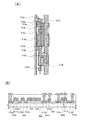
本実施の形態における発光素子の構造例について図1を用いて説明する。図1は、本実施の形態における発光素子の構造例を説明するための図である。 A structural example of the light-emitting element in this embodiment will be described with reference to FIGS. FIG. 1 is a diagram for explaining a structural example of a light-emitting element in this embodiment.
発光素子は、図1(A)に示すように電極層(EDともいう)101と、発光層(LEともいう)102と、電極層103と、を含む。
The light-emitting element includes an electrode layer (also referred to as ED) 101, a light-emitting layer (also referred to as LE) 102, and an
なお、電極層とは、電極としての機能を有する層のことをいう。 Note that the electrode layer refers to a layer having a function as an electrode.
電極層101は、発光素子の電極としての機能を有する。
The
発光層102は、電圧が印加されることにより特定の色を呈する光を射出する層である。発光層102は、M個の発光ユニット(Mは自然数)を含む。
The
また、一般的に電圧とは、ある二点間における電位の差(電位差ともいう)のことをいう。しかし、電圧及び電位の値は、回路図などにおいていずれもボルト(V)で表されることがあるため、区別が困難である。そこで、本明細書では、特に指定する場合を除き、ある一点の電位と基準となる電位(基準電位ともいう)との電位差を、該一点の電圧として用いる場合がある。 In general, a voltage refers to a difference in potential between two points (also referred to as a potential difference). However, the values of voltage and potential are both expressed in volts (V) in circuit diagrams and the like, and thus are difficult to distinguish. Therefore, in this specification, a potential difference between a potential at one point and a reference potential (also referred to as a reference potential) may be used as the voltage at the one point unless otherwise specified.
電極層103は、発光素子の電極としての機能を有する。
The
図1(A)に示す発光素子は、一対の電極(電極層101及び電極層103)、及び上記一対の電極に重畳する発光層(発光層102)を有し、上記一対の電極の間に印加される電圧に応じて発光層102が発光することにより光を射出する。
A light-emitting element illustrated in FIG. 1A includes a pair of electrodes (an
さらに、発光素子の各構成要素について以下に説明する。 Further, each component of the light emitting element will be described below.
電極層101及び電極層103のうち、一方の電極層(第1の電極層ともいう)は、図1(B)に示すように、導電層111(RFLともいう)と、導電層112(TiLともいう)と、導電層113(MOLともいう)と、を有する。
One electrode layer (also referred to as a first electrode layer) of the
導電層111としては、光を反射する材料を有する金属層を用いることができる。光を反射する材料の層としては、例えばアルミニウム、又はアルミニウムと他の金属(チタン、ネオジム、ニッケル、及びランタンの一つ又は複数)との合金材料の層を用いることができる。アルミニウムは、抵抗値が低く、光の反射率が高い。また、アルミニウムは、地殻における存在量が多く、安価であるため、アルミニウムを用いることにより発光素子の作製コストを低減することができる。また、銀を用いてもよい。
As the
導電層112としては、チタンを含む導電層を用いることができ、例えばチタン層又は酸化チタン層を用いることができる。なお、チタン酸化物と導電性を有するチタン化合物の混在層により導電層112を構成してもよい。導電層111の上に導電層112を設けることにより、導電層111の酸化又は電食を抑制することができる。
As the
また、導電層112には、熱処理が行われていることが好ましい。上記熱処理により、導電層112と導電層113の密着性をさらに良くすることができる。
The
導電層113は、導電層112と発光層102の間に設けられる。導電層113としては、導電性が高く、導電層111の材料より仕事関数の高い金属酸化物の層を用いることができる。さらに、導電層113は、光を透過する機能を有する。導電層113としては、例えば酸化インジウム(In2O3)、酸化スズ(SnO2)、酸化亜鉛(ZnO)、酸化インジウム−酸化スズ(In2O3−SnO2、ITOともいう)、酸化珪素を含む酸化インジウム−酸化スズ(ITO−SiOxともいう)、酸化インジウム−酸化亜鉛(In2O3―ZnO)などの金属酸化物、シリコン、酸化シリコン、あるいは窒素を含む前記金属酸化物などを用いることができる。また、上記材料の積層により導電層113を構成することもできる。上記材料は、導電層112及び発光層102と接しても素子特性の低下を抑制することができるため、好ましい。
The
また、発光層102は、蛍光材料又は燐光材料などの発光材料を含む層を用いることができる。
For the light-emitting
電極層101及び電極層103のうち、他方の電極層(第2の電極層ともいう)は、光を透過する。第2の電極層としては、例えば酸化インジウム、酸化スズ、酸化亜鉛、酸化インジウム−酸化スズ、酸化珪素を含む酸化インジウム−酸化スズ、酸化インジウム−酸化亜鉛などの金属酸化物、シリコン、酸化シリコン、あるいは窒素を含む前記金属酸化物を用いることができる。また、第2の電極層としては、銀、マグネシウム、並びに銀及びマグネシウムの合金の層を用いることができる。また、上記材料の積層により、第2の電極層を構成することもできる。
Of the
発光素子の構造が電極層103を介して光を射出する構造の場合には、電極層101が導電層111、導電層112、及び導電層113の積層であり、電極層103が光を透過する導電層である。また、発光素子の構造が電極層101を介して光を射出する構造の場合には、電極層103が導電層111、導電層112、及び導電層113の積層であり、電極層101が光を透過する導電層である。
In the case where the light-emitting element has a structure in which light is emitted through the
さらに、発光層102が射出する光が、第1の電極層及び第2の電極層の間において、干渉して強められるように発光素子を構成してもよい。すなわち、光学距離を最適化することにより、発光層102が射出する光を第1の電極層及び第2の電極層の間において干渉させて強めるようにしてもよい。例えば、電極層101から電極層103までの長さ、すなわち発光層102の膜厚と発光層102の屈折率との積が、所望の光の波長のN/2倍(Nは自然数)になるように、電極層101から電極層103までの長さを調整してもよい。また、導電層113が光を透過する場合、導電層111から電極層103までの長さと発光層102の屈折率との積が、所望の光の波長のN/2倍(Nは自然数)になるように、導電層111から電極層103までの長さを調整してもよい。これにより、発光素子の光の強度をさらに高くすることができる。上記調整された構造を光共振構造ともいう。また、上記調整された構造をマイクロキャビティ構造ともいうことができる。
Further, the light-emitting element may be configured such that light emitted from the light-emitting
なお、導電層113が光を透過する場合、導電層113の厚さを調整することにより光路長を調整することが好ましい。なぜならば、導電層113は、光を透過し、フォトリソグラフィ技術により導電層113を形成することができるため、製造工程が容易であり、厚さの調整も容易であるからである。
Note that in the case where the
以上が図1に示す発光素子の構造例の説明である。 The above is the description of the structure example of the light-emitting element illustrated in FIG.
図1を用いて説明したように、本実施の形態における発光素子の一例では、第1の電極層を、光を反射する第1の導電層と、チタンを含む第2の導電層と、光を透過し、第1の導電層の材料より仕事関数の大きい金属酸化物を含む第3の導電層の積層にすることにより、発光素子の電極による電圧損失を低減させ、電極における電荷の注入特性を改善することができるため、発光素子の駆動電圧を低減することができる。 As described with reference to FIG. 1, in the example of the light-emitting element in this embodiment, the first electrode layer includes a first conductive layer that reflects light, a second conductive layer containing titanium, and light. And the third conductive layer including a metal oxide having a work function larger than that of the material of the first conductive layer, thereby reducing voltage loss due to the electrode of the light-emitting element, and charge injection characteristics in the electrode Therefore, the driving voltage of the light emitting element can be reduced.
さらに、本発明の一態様では、光共振構造を、光を透過する機能を有し、かつフォトリソグラフィ技術を用いて形成することが可能な金属酸化物を含む導電層の厚さを変えるだけで調整でき、上記調整を行うことにより、発光素子の光の強度を高くすることができる。 Further, according to one embodiment of the present invention, the optical resonant structure has a function of transmitting light, and the thickness of a conductive layer including a metal oxide that can be formed using a photolithography technique is changed. The light intensity of the light emitting element can be increased by performing the above adjustment.
よって、発光素子の素子特性を向上させることができる。 Therefore, element characteristics of the light emitting element can be improved.
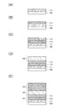
本実施の形態における発光素子の作製方法例について図2を用いて説明する。なお、図2では、一例として電極層103側から光を取り出す構造の発光素子の例について示す。
An example of a method for manufacturing the light-emitting element in this embodiment will be described with reference to FIGS. Note that FIG. 2 illustrates an example of a light-emitting element having a structure in which light is extracted from the
まず、図2(A)に示すように、被素子形成層100の上に導電層111を形成する。
First, as illustrated in FIG. 2A, the
例えば、スパッタリング法などを用いて導電層111に適用可能な導電膜を形成することにより導電層111を形成することができる。
For example, the
次に、図2(B)に示すように、導電層111の上に導電層112を形成する。
Next, as illustrated in FIG. 2B, the
例えば、スパッタリング法などを用いて導電層112に適用可能な導電膜を形成することにより導電層112を形成することができる。
For example, the
さらに、熱処理を行う。例えば、200℃以上300℃以下の範囲の温度で熱処理を行う。上記熱処理により、導電層112の一部を酸化させることができる。
Further, heat treatment is performed. For example, the heat treatment is performed at a temperature in the range of 200 ° C. to 300 ° C. Through the heat treatment, part of the
次に、図2(C)に示すように、導電層112の上に導電層113を形成する。
Next, as illustrated in FIG. 2C, a
例えば、スパッタリング法などを用いて導電層113に適用可能な導電膜を形成することにより導電層113を形成することができる。
For example, the
次に、図2(D)に示すように、導電層113の上に発光層102を形成する。
Next, as illustrated in FIG. 2D, the light-emitting
例えば、蒸着法(真空蒸着法を含む)、インクジェット法、又は塗布法などの方法を用いて発光層102に適用可能な材料の膜を形成することにより発光層102を形成することができる。
For example, the light-emitting
次に、図2(E)に示すように、発光層102の上に電極層103を形成する。
Next, as illustrated in FIG. 2E, the
例えば、スパッタリング法などを用いて電極層103に適用可能な導電膜を形成することにより電極層103を形成することができる。
For example, the
以上が発光素子の作製方法例の説明である。 The above is the description of the method for manufacturing the light-emitting element.
図2を用いて説明したように、本実施の形態における発光素子の作製方法の一例では、光を反射する第1の導電層、チタンを含む第2の導電層を順に形成した後に熱処理を行い、その後第2の導電層の上に、第1の導電層の材料より仕事関数の大きい金属酸化物を含む第3の導電層を形成して電極層を作製することにより、第3の導電層の酸素欠損による応力の発生を抑制することができるため、第2の導電層と第3の導電層の密着性を高めることができる。 As described with reference to FIGS. 2A and 2B, in the example of the method for manufacturing the light-emitting element in this embodiment, heat treatment is performed after the first conductive layer that reflects light and the second conductive layer containing titanium are sequentially formed. Then, a third conductive layer containing a metal oxide having a work function larger than that of the material of the first conductive layer is formed on the second conductive layer to produce an electrode layer. Since the generation of stress due to oxygen deficiency can be suppressed, the adhesion between the second conductive layer and the third conductive layer can be improved.
(実施の形態2)
本実施の形態では、上記実施の形態に示す発光素子における発光層(LE)の構造例について説明する。
(Embodiment 2)
In this embodiment, structural examples of the light-emitting layer (LE) in the light-emitting element described in the above embodiment will be described.
発光層は、M個の発光ユニット(LEUともいう)を含む。 The light emitting layer includes M light emitting units (also referred to as LEU).
さらに、本実施の形態における発光ユニットの構造例について図3を用いて説明する。図3は、本実施の形態における発光ユニットの構造例を示す断面模式図である。 Further, a structural example of the light-emitting unit in this embodiment will be described with reference to FIGS. FIG. 3 is a schematic cross-sectional view showing a structural example of the light emitting unit in the present embodiment.
図3(A)に示す発光ユニットは、エレクトロルミネセンス層(ELLともいう)121aを有する。 The light-emitting unit illustrated in FIG. 3A includes an electroluminescent layer (also referred to as ELL) 121a.
エレクトロルミネセンス層121aは、発光材料を含む層である。
The
また、図3(B)に示す発光ユニットは、エレクトロルミネセンス層121bと、正孔注入層(HILともいう)122と、正孔輸送層(HTLともいう)123と、電子輸送層(ETLともいう)124と、電子注入層(EILともいう)125と、を含む。
3B includes an
エレクトロルミネセンス層121bは、発光材料を含む層である。
The
また、エレクトロルミネセンス層121bは、正孔輸送層123上に設けられる。なお、正孔輸送層123を設けない場合、エレクトロルミネセンス層121bは、正孔注入層122上に設けられる。
In addition, the
正孔注入層122は、正孔を注入するための層である。なお、必ずしも正孔注入層122を設けなくてもよい。
The
正孔注入層122を設ける場合、正孔輸送層123は、正孔注入層122上に設けられる。
When the
正孔輸送層123は、エレクトロルミネセンス層121bに正孔を輸送するための層である。なお、必ずしも正孔輸送層123を設けなくてもよい。
The
電子輸送層124は、エレクトロルミネセンス層121b上に設けられる。
The
電子輸送層124は、エレクトロルミネセンス層121bに電子を輸送するための層である。なお、必ずしも電子輸送層124を設けなくてもよい。
The
電子輸送層124を設ける場合、電子注入層125は、電子輸送層124上に設けられる。なお、電子輸送層124を設けない場合、電子注入層125は、エレクトロルミネセンス層121b上に設けられる。
When the
電子注入層125は、電子を注入するための層である。
The
さらに、図3(A)及び図3(B)に示す発光ユニットの各構成要素について説明する。 Further, each component of the light-emitting unit illustrated in FIGS. 3A and 3B will be described.
エレクトロルミネセンス層121a及びエレクトロルミネセンス層121bとしては、例えば蛍光を発する化合物又は燐光を発する化合物、及びホスト材料を含む層を用いることができる。
As the
蛍光を発する化合物としては、例えば青色を呈する光を発する蛍光材料(青色蛍光材料ともいう)、緑色を呈する光を発する蛍光材料(緑色蛍光材料ともいう)、黄色を呈する光を発する蛍光材料(黄色蛍光材料ともいう)、又は赤色を呈する光を発する蛍光材料(赤色蛍光材料ともいう)などを用いることができる。 Examples of fluorescent compounds include fluorescent materials that emit blue light (also referred to as blue fluorescent materials), fluorescent materials that emit green light (also referred to as green fluorescent materials), and fluorescent materials that emit yellow light (yellow). (Also referred to as a fluorescent material) or a fluorescent material that emits red light (also referred to as a red fluorescent material) or the like can be used.
青色蛍光材料としては、例えばN,N’−ビス[4−(9H−カルバゾール−9−イル)フェニル]−N,N’−ジフェニルスチルベン−4,4’−ジアミン(YGA2S(略称)ともいう)、4−(9H−カルバゾール−9−イル)−4’−(10−フェニル−9−アントリル)トリフェニルアミン(YGAPA(略称)ともいう)、4−(10−フェニル−9−アントリル)−4’−(9−フェニル−9H−カルバゾール−3−イル)トリフェニルアミン(PCBAPA(略称)ともいう)などを用いることができる。 As a blue fluorescent material, for example, N, N′-bis [4- (9H-carbazol-9-yl) phenyl] -N, N′-diphenylstilbene-4,4′-diamine (also referred to as YGA2S (abbreviation)) 4- (9H-carbazol-9-yl) -4 ′-(10-phenyl-9-anthryl) triphenylamine (also referred to as YGAPA (abbreviation)), 4- (10-phenyl-9-anthryl) -4 '-(9-phenyl-9H-carbazol-3-yl) triphenylamine (also referred to as PCBAPA (abbreviation)) and the like can be used.
緑色蛍光材料としては、例えばN−(9,10−ジフェニル−2−アントリル)−N,9−ジフェニル−9H−カルバゾール−3−アミン(2PCAPA(略称)ともいう)、N−[9,10−ビス(1,1’−ビフェニル−2−イル)−2−アントリル]−N,9−ジフェニル−9H−カルバゾール−3−アミン(2PCABPhA(略称)ともいう)、N−(9,10−ジフェニル−2−アントリル)−N,N’,N’−トリフェニル−1,4−フェニレンジアミン(2DPAPA(略称)ともいう)、N−[9,10−ビス(1,1’−ビフェニル−2−イル)−2−アントリル]−N,N’,N’−トリフェニル−1,4−フェニレンジアミン(2DPABPhA(略称)ともいう)、N−[9,10−ビス(1,1’−ビフェニル−2−イル)]−N−[4−(9H−カルバゾール−9−イル)フェニル]−N−フェニルアントラセン−2−アミン(2YGABPhA(略称)ともいう)、N,N,9−トリフェニルアントラセン−9−アミン(DPhAPhA(略称)ともいう)などが挙げられる。 Examples of the green fluorescent material include N- (9,10-diphenyl-2-anthryl) -N, 9-diphenyl-9H-carbazol-3-amine (also referred to as 2PCAPA (abbreviation)), N- [9,10- Bis (1,1′-biphenyl-2-yl) -2-anthryl] -N, 9-diphenyl-9H-carbazol-3-amine (also referred to as 2PCABPhA (abbreviation)), N- (9,10-diphenyl- 2-anthryl) -N, N ′, N′-triphenyl-1,4-phenylenediamine (also referred to as 2DPAPA (abbreviation)), N- [9,10-bis (1,1′-biphenyl-2-yl) ) -2-anthryl] -N, N ′, N′-triphenyl-1,4-phenylenediamine (also referred to as 2DPABPhA (abbreviation)), N- [9,10-bis (1,1′-biphenyl) 2-yl)]-N- [4- (9H-carbazol-9-yl) phenyl] -N-phenylanthracen-2-amine (also referred to as 2YGABPhA (abbreviation)), N, N, 9-triphenylanthracene- And 9-amine (also referred to as DPhAPhA (abbreviation)).
また、黄色蛍光材料としては、例えばルブレン、又は5,12−ビス(1,1’−ビフェニル−4−イル)−6,11−ジフェニルテトラセン(BPT(略称)ともいう)などを用いることができる。 As a yellow fluorescent material, for example, rubrene or 5,12-bis (1,1′-biphenyl-4-yl) -6,11-diphenyltetracene (also referred to as BPT (abbreviation)) can be used. .
また、赤色蛍光材料としては、例えばN,N,N’,N’−テトラキス(4−メチルフェニル)テトラセン−5,11−ジアミン(p−mPhTD(略称)ともいう)、又は7,14−ジフェニル−N,N,N’,N’−テトラキス(4−メチルフェニル)アセナフト[1,2−a]フルオランテン−3,10−ジアミン(p−mPhAFD(略称)ともいう)などを用いることができる。 Examples of red fluorescent materials include N, N, N ′, N′-tetrakis (4-methylphenyl) tetracene-5,11-diamine (also referred to as p-mPhTD (abbreviation)) or 7,14-diphenyl. -N, N, N ', N'-tetrakis (4-methylphenyl) acenaphtho [1,2-a] fluoranthene-3,10-diamine (also referred to as p-mPhAFD (abbreviation)) and the like can be used.
また、燐光を発する化合物としては、例えば青色を呈する光を発する燐光材料(青色燐光材料ともいう)、緑色を呈する光を発する燐光材料(緑色燐光材料ともいう)、黄色を呈する光を発する燐光材料(黄色燐光材料ともいう)、橙色を呈する光を発する燐光材料(橙色燐光材料ともいう)、又は赤色を呈する光を発する燐光材料(赤色燐光材料ともいう)などを用いることができる。 Examples of the phosphorescent compound include phosphorescent materials that emit blue light (also referred to as blue phosphorescent materials), phosphorescent materials that emit green light (also referred to as green phosphorescent materials), and phosphorescent materials that emit yellow light. (Also referred to as a yellow phosphorescent material), a phosphorescent material that emits orange light (also referred to as an orange phosphorescent material), a phosphorescent material that emits red light (also referred to as a red phosphorescent material), or the like can be used.
青色燐光材料としては、例えばビス[2−(4’,6’−ジフルオロフェニル)ピリジナト−N,C2’]イリジウム(III)テトラキス(1−ピラゾリル)ボラート(FIr6(略称)ともいう)、ビス[2−(4’,6’−ジフルオロフェニル)ピリジナト−N,C2’]イリジウム(III)ピコリナート(FIrpic(略称)ともいう)、ビス{2−[3’,5’−ビス(トリフルオロメチル)フェニル]ピリジナト−N,C2’}イリジウム(III)ピコリナート(Ir(CF3ppy)2(pic)(略称)ともいう)、又はビス[2−(4’,6’−ジフルオロフェニル)ピリジナト−N,C2’]イリジウム(III)アセチルアセトナート(FIr(acac)(略称)ともいう)などを用いることができる。 As a blue phosphorescent material, for example, bis [2- (4 ′, 6′-difluorophenyl) pyridinato-N, C 2 ′ ] iridium (III) tetrakis (1-pyrazolyl) borate (also referred to as FIr6 (abbreviation)), bis [2- (4 ′, 6′-difluorophenyl) pyridinato-N, C 2 ′ ] iridium (III) picolinate (also referred to as FIrpic (abbreviation)), bis {2- [3 ′, 5′-bis (trifluoro) Methyl) phenyl] pyridinato-N, C2 ′ } iridium (III) picolinate (also referred to as Ir (CF 3 ppy) 2 (pic) (abbreviation)) or bis [2- (4 ′, 6′-difluorophenyl) Pyridinato-N, C 2 ′ ] iridium (III) acetylacetonate (also referred to as FIr (acac) (abbreviation)) and the like can be used.
緑色燐光材料としては、例えばトリス(2−フェニルピリジナト−N,C2’)イリジウム(III)(Ir(ppy)3(略称)ともいう)、ビス(2−フェニルピリジナト−N,C2’)イリジウム(III)アセチルアセトナート(Ir(ppy)2(acac)(略称)ともいう)、ビス(1,2−ジフェニル−1H−ベンゾイミダゾラト)イリジウム(III)アセチルアセトナート(Ir(pbi)2(acac)(略称)ともいう)、ビス(ベンゾ[h]キノリナト)イリジウム(III)アセチルアセトナート(Ir(bzq)2(acac)(略称)ともいう)、又はトリス(ベンゾ[h]キノリナト)イリジウム(III)(Ir(bzq)3(略称)ともいう)などを用いることができる。 Examples of the green phosphorescent material include tris (2-phenylpyridinato-N, C 2 ′ ) iridium (III) (also referred to as Ir (ppy) 3 (abbreviation)), bis (2-phenylpyridinato-N, C 2 ′ ) iridium (III) acetylacetonate (also referred to as Ir (ppy) 2 (acac) (abbreviation)), bis (1,2-diphenyl-1H-benzimidazolato) iridium (III) acetylacetonate (Ir (Pbi) 2 (acac) (abbreviation)), bis (benzo [h] quinolinato) iridium (III) acetylacetonate (Ir (bzq) 2 (acac) (abbreviation)), or tris (benzo [ h] quinolinato) iridium (III) (also referred to as Ir (bzq) 3 (abbreviation)) and the like can be used.
黄色燐光材料としては、例えばビス(2,4−ジフェニル−1,3−オキサゾラト−N,C2’)イリジウム(III)アセチルアセトナート(Ir(dpo)2(acac)(略称)ともいう)、ビス[2−(4’−パーフルオロフェニルフェニル)ピリジナト]イリジウム(III)アセチルアセトナート(Ir(p−PF−ph)2(acac)(略称)ともいう)、ビス(2−フェニルベンゾチアゾラト−N,C2’)イリジウム(III)アセチルアセトナート(Ir(bt)2(acac)(略称)ともいう)、(アセチルアセトナート)ビス[2,3−ビス(4−フルオロフェニル)−5−メチルピラジナト]イリジウム(III)(Ir(Fdppr−Me)2(acac)(略称)ともいう)、又は(アセチルアセトナート)ビス{2−(4−メトキシフェニル)−3,5−ジメチルピラジナト}イリジウム(III)(Ir(dmmoppr)2(acac)(略称)ともいう)などを用いることができる。 As a yellow phosphorescent material, for example, bis (2,4-diphenyl-1,3-oxazolate-N, C 2 ′ ) iridium (III) acetylacetonate (also referred to as Ir (dpo) 2 (acac) (abbreviation)), Bis [2- (4′-perfluorophenylphenyl) pyridinato] iridium (III) acetylacetonate (also referred to as Ir (p-PF-ph) 2 (acac) (abbreviation)), bis (2-phenylbenzothiazola) To-N, C 2 ′ ) iridium (III) acetylacetonate (also referred to as Ir (bt) 2 (acac) (abbreviation)), (acetylacetonato) bis [2,3-bis (4-fluorophenyl)- 5 methylpyrazinato] iridium (III) (Ir (Fdppr-Me) also referred to as 2 (acac) (abbreviation)), or (acetylacetonato Over G) also referred to as bis {2- (4-methoxyphenyl) -3,5-dimethylpyrazinato} iridium (III) (Ir (dmmoppr) 2 (acac) (abbreviation)) or the like can be used.
橙色燐光材料としては、例えばトリス(2−フェニルキノリナト−N,C2’)イリジウム(III)(Ir(pq)3(略称)ともいう)、ビス(2−フェニルキノリナト−N,C2’)イリジウム(III)アセチルアセトナート(Ir(pq)2(acac)(略称)ともいう)、(アセチルアセトナート)ビス(3,5−ジメチル−2−フェニルピラジナト)イリジウム(III)(Ir(mppr−Me)2(acac)(略称)ともいう)、(アセチルアセトナート)ビス(5−イソプロピル−3−メチル−2−フェニルピラジナト)イリジウム(III)(Ir(mppr−iPr)2(acac)(略称)ともいう)などを用いることができる。 Examples of the orange phosphorescent material include tris (2-phenylquinolinato-N, C 2 ′ ) iridium (III) (also referred to as Ir (pq) 3 (abbreviation)), bis (2-phenylquinolinato-N, C 2). ' ) Iridium (III) acetylacetonate (also referred to as Ir (pq) 2 (acac) (abbreviation)), (acetylacetonato) bis (3,5-dimethyl-2-phenylpyrazinato) iridium (III) ( Ir (mppr-Me) 2 (acac) (abbreviation)), (acetylacetonato) bis (5-isopropyl-3-methyl-2-phenylpyrazinato) iridium (III) (Ir (mppr-iPr) 2 (acac) (abbreviation)) and the like can be used.
赤色燐光材料としては、例えばビス[2−(2’−ベンゾ[4,5−α]チエニル)ピリジナト−N,C3’]イリジウム(III)アセチルアセトナート(Ir(btp)2(acac))、ビス(1−フェニルイソキノリナト−N,C2’)イリジウム(III)アセチルアセトナート(Ir(piq)2(acac)(略称)ともいう)、(アセチルアセトナート)ビス[2,3−ビス(4−フルオロフェニル)キノキサリナト]イリジウム(III)(Ir(Fdpq)2(acac)(略称)ともいう)、(アセチルアセトナート)ビス(2,3,5−トリフェニルピラジナト)イリジウム(III)(Ir(tppr)2(acac)(略称)ともいう)、(ジピバロイルメタナト)ビス(2,3,5−トリフェニルピラジナト)イリジウム(III)(Ir(tppr)2(dpm)(略称)ともいう)、又は2,3,7,8,12,13,17,18−オクタエチル−21H,23H−ポルフィリン白金(II)(PtOEP(略称)ともいう)などを用いることができる。 Examples of the red phosphorescent material include bis [2- (2′-benzo [4,5-α] thienyl) pyridinato-N, C 3 ′ ] iridium (III) acetylacetonate (Ir (btp) 2 (acac)). Bis (1-phenylisoquinolinato-N, C 2 ′ ) iridium (III) acetylacetonate (also referred to as Ir (piq) 2 (acac) (abbreviation)), (acetylacetonato) bis [2,3- Bis (4-fluorophenyl) quinoxalinato] iridium (III) (also referred to as Ir (Fdpq) 2 (acac) (abbreviation)), (acetylacetonato) bis (2,3,5-triphenylpyrazinato) iridium ( III) also referred to as (Ir (tppr) 2 (acac) (abbreviation)), (dipivaloylmethanato) bis (2,3,5-triphenyl pyrazinium G) iridium (III) (Ir (tppr) 2 (dpm) ( abbreviation) and also referred to), or 2,3,7,8,12,13,17,18-octaethyl-21H, 23H-porphyrin platinum (II) (Also referred to as PtOEP (abbreviation)) can be used.
また、燐光を発する化合物としては、希土類金属錯体を用いることができる。希土類金属錯体の発光は、希土類金属イオンからの発光(異なる多重度間の電子遷移)であるため、燐光を発する化合物として用いることができる。燐光を発する化合物としては、例えばトリス(アセチルアセトナート)(モノフェナントロリン)テルビウム(III)(Tb(acac)3(Phen)(略称)ともいう)、トリス(1,3−ジフェニル−1,3−プロパンジオナト)(モノフェナントロリン)ユーロピウム(III)(Eu(DBM)3(Phen)(略称)ともいう)、トリス[1−(2−テノイル)−3,3,3−トリフルオロアセトナト](モノフェナントロリン)ユーロピウム(III)(Eu(TTA)3(Phen)(略称)ともいう)などを用いることができる。 A rare earth metal complex can be used as the phosphorescent compound. Since the light emission of the rare earth metal complex is light emission from the rare earth metal ions (electron transition between different multiplicity), it can be used as a phosphorescent compound. Examples of the phosphorescent compound include tris (acetylacetonato) (monophenanthroline) terbium (III) (also referred to as Tb (acac) 3 (Phen) (abbreviation)), tris (1,3-diphenyl-1,3- Propanedionato) (monophenanthroline) europium (III) (also referred to as Eu (DBM) 3 (Phen) (abbreviation)), tris [1- (2-thenoyl) -3,3,3-trifluoroacetonato] ( Monophenanthroline) europium (III) (also referred to as Eu (TTA) 3 (Phen) (abbreviation)) and the like can be used.
なお、エレクトロルミネセンス層121a及びエレクトロルミネセンス層121bにおいて、蛍光を発する化合物又は燐光を発する化合物は上記ホスト材料中にゲスト材料として分散されている。ホスト材料としては、例えばゲスト材料よりも最低空軌道準位(LUMO準位)が高く、最高被占有軌道準位(HOMO準位)が低い物質を用いることが好ましい。
Note that in the
ホスト材料としては、例えば金属錯体、複素環化合物、縮合芳香族化合物、又は芳香族アミン化合物などを用いることができる。 As the host material, for example, a metal complex, a heterocyclic compound, a condensed aromatic compound, an aromatic amine compound, or the like can be used.
例えば、ホスト材料としては、トリス(8−キノリノラト)アルミニウム(III)(Alq(略称)ともいう)、トリス(4−メチル−8−キノリノラト)アルミニウム(III)(Almq3(略称)ともいう)、ビス(10−ヒドロキシベンゾ[h]キノリナト)ベリリウム(II)(BeBq2(略称)ともいう)、ビス(2−メチル−8−キノリノラト)(4−フェニルフェノラト)アルミニウム(III)(BAlq(略称)ともいう)、ビス(8−キノリノラト)亜鉛(II)(Znq(略称)ともいう)、ビス[2−(2−ベンゾオキサゾリル)フェノラト]亜鉛(II)(ZnPBO(略称)ともいう)、ビス[2−(2−ベンゾチアゾリル)フェノラト]亜鉛(II)(ZnBTZ(略称)ともいう)、2−(4−ビフェニリル)−5−(4−tert−ブチルフェニル)−1,3,4−オキサジアゾール(PBD(略称)ともいう)、1,3−ビス[5−(p−tert−ブチルフェニル)−1,3,4−オキサジアゾール−2−イル]ベンゼン(OXD−7(略称)ともいう)、3−(4−ビフェニリル)−4−フェニル−5−(4−tert−ブチルフェニル)−1,2,4−トリアゾール(TAZ(略称)ともいう)、2,2’,2’’−(1,3,5−ベンゼントリイル)トリス(1−フェニル−1H−ベンゾイミダゾール)(TPBI(略称)ともいう)、バソフェナントロリン(BPhen(略称)ともいう)、バソキュプロイン(BCP(略称)ともいう)、CzPA、3,6−ジフェニル−9−[4−(10−フェニル−9−アントリル)フェニル]−9H−カルバゾール(DPCzPA(略称)ともいう)、DNA、t−BuDNA、9,9’−ビアントリル(BANT(略称)ともいう)、9,9’−(スチルベン−3,3’−ジイル)ジフェナントレン(DPNS(略称)ともいう)、9,9’−(スチルベン−4,4’−ジイル)ジフェナントレン(DPNS2(略称)ともいう)、3,3’,3’’−(ベンゼン−1,3,5−トリイル)トリピレン(TPB3(略称)ともいう)、DPAnth、6,12−ジメトキシ−5,11−ジフェニルクリセン、N,N−ジフェニル−9−[4−(10−フェニル−9−アントリル)フェニル]−9H−カルバゾール−3−アミン(CzA1PA(略称)ともいう)、4−(10−フェニル−9−アントリル)トリフェニルアミン(DPhPA(略称)ともいう)、N,9−ジフェニル−N−[4−(10−フェニル−9−アントリル)フェニル]−9H−カルバゾール−3−アミン(PCAPA(略称)ともいう)、N,9−ジフェニル−N−{4−[4−(10−フェニル−9−アントリル)フェニル]フェニル}−9H−カルバゾール−3−アミン(PCAPBA(略称)ともいう)、N−(9,10−ジフェニル−2−アントリル)−N,9−ジフェニル−9H−カルバゾール−3−アミン(2PCAPA(略称)ともいう)、NPB、TPD、DFLDPBi、又はBSPBなどを用いることができる。 For example, as a host material, tris (8-quinolinolato) aluminum (III) (also referred to as Alq (abbreviation)), tris (4-methyl-8-quinolinolato) aluminum (III) (also referred to as Almq 3 (abbreviation)), Bis (10-hydroxybenzo [h] quinolinato) beryllium (II) (also referred to as BeBq 2 (abbreviation)), bis (2-methyl-8-quinolinolato) (4-phenylphenolato) aluminum (III) (BAlq (abbreviation) )), Bis (8-quinolinolato) zinc (II) (also referred to as Znq (abbreviation)), bis [2- (2-benzoxazolyl) phenolato] zinc (II) (also referred to as ZnPBO (abbreviation)) Bis [2- (2-benzothiazolyl) phenolato] zinc (II) (also referred to as ZnBTZ (abbreviation)), 2- (4-bi Phenylyl) -5- (4-tert-butylphenyl) -1,3,4-oxadiazole (also referred to as PBD (abbreviation)), 1,3-bis [5- (p-tert-butylphenyl) -1 , 3,4-oxadiazol-2-yl] benzene (also referred to as OXD-7 (abbreviation)), 3- (4-biphenylyl) -4-phenyl-5- (4-tert-butylphenyl) -1, 2,4-triazole (also referred to as TAZ (abbreviation)), 2,2 ′, 2 ″-(1,3,5-benzenetriyl) tris (1-phenyl-1H-benzimidazole) (TPBI (abbreviation)) Also bathophenanthroline (also referred to as BPhen (abbreviation)), bathocuproin (also referred to as BCP (abbreviation)), CzPA, 3,6-diphenyl-9- [4- (10-phenyl-9-anthryl) fur. Nyl] -9H-carbazole (also referred to as DPCzPA (abbreviation)), DNA, t-BuDNA, 9,9′-bianthryl (also referred to as BANT (abbreviation)), 9,9 ′-(stilbene-3,3′-diyl) ) Diphenanthrene (also referred to as DPNS (abbreviation)), 9,9 ′-(stilbene-4,4′-diyl) diphenanthrene (also referred to as DPNS2 (abbreviation)), 3,3 ′, 3 ″-(benzene- 1,3,5-triyl) tripylene (also referred to as TPB3 (abbreviation)), DPAnth, 6,12-dimethoxy-5,11-diphenylchrysene, N, N-diphenyl-9- [4- (10-phenyl-9) -Anthryl) phenyl] -9H-carbazol-3-amine (also referred to as CzA1PA (abbreviation)), 4- (10-phenyl-9-anthryl) triphenylamine (DPh) PA (abbreviation)), N, 9-diphenyl-N- [4- (10-phenyl-9-anthryl) phenyl] -9H-carbazol-3-amine (also referred to as PCAPA (abbreviation)), N, 9 -Diphenyl-N- {4- [4- (10-phenyl-9-anthryl) phenyl] phenyl} -9H-carbazol-3-amine (also referred to as PCAPBA (abbreviation)), N- (9,10-diphenyl- 2-anthryl) -N, 9-diphenyl-9H-carbazol-3-amine (also referred to as 2PCAPA (abbreviation)), NPB, TPD, DFLDPBi, or BSPB can be used.
また、上記ホスト材料を複数用いてエレクトロルミネセンス層121a及びエレクトロルミネセンス層121bを構成することもできる。
Alternatively, the
ゲスト材料をホスト材料に分散させた層によりエレクトロルミネセンス層121a及びエレクトロルミネセンス層121bを構成することにより、エレクトロルミネセンス層121a及びエレクトロルミネセンス層121bの結晶化を抑制することができ、また、ゲスト材料の濃度消光を抑制することができる。
By forming the
また、エレクトロルミネセンス層121a及びエレクトロルミネセンス層121bとしては、高分子化合物の発光物質を含む層を用いることができる。
In addition, as the
高分子化合物の発光物質としては、例えばポリ(9,9−ジオクチルフルオレン−2,7−ジイル)(PFO(略称)ともいう)、ポリ[(9,9−ジオクチルフルオレン−2,7−ジイル)−co−(2,5−ジメトキシベンゼン−1,4−ジイル)](PF−DMOP(略称)ともいう)、ポリ{(9,9−ジオクチルフルオレン−2,7−ジイル)−co−[N,N’−ジ−(p−ブチルフェニル)−1,4−ジアミノベンゼン]}(TAB−PFH(略称)ともいう)、ポリ(p−フェニレンビニレン)(PPV(略称)ともいう)、ポリ[(9,9−ジヘキシルフルオレン−2,7−ジイル)−alt−co−(ベンゾ[2,1,3]チアジアゾール−4,7−ジイル)](PFBT(略称)ともいう)、ポリ[(9,9−ジオクチル−2,7−ジビニレンフルオレニレン)−alt−co−(2−メトキシ−5−(2−エチルヘキシロキシ)−1,4−フェニレン)]、ポリ[2−メトキシ−5−(2’−エチルヘキソキシ)−1,4−フェニレンビニレン](MEH−PPV(略称)ともいう)、ポリ(3−ブチルチオフェン−2,5−ジイル)(R4−PAT(略称)ともいう)、ポリ{[9,9−ジヘキシル−2,7−ビス(1−シアノビニレン)フルオレニレン]−alt−co−[2,5−ビス(N,N’−ジフェニルアミノ)−1,4−フェニレン]}、又はポリ{[2−メトキシ−5−(2−エチルヘキシロキシ)−1,4−ビス(1−シアノビニレンフェニレン)]−alt−co−[2,5−ビス(N,N’−ジフェニルアミノ)−1,4−フェニレン]}(CN−PPV−DPD(略称)ともいう)などを用いることができる。 As a light-emitting substance of a polymer compound, for example, poly (9,9-dioctylfluorene-2,7-diyl) (also referred to as PFO (abbreviation)), poly [(9,9-dioctylfluorene-2,7-diyl) -Co- (2,5-dimethoxybenzene-1,4-diyl)] (also referred to as PF-DMOP (abbreviation)), poly {(9,9-dioctylfluorene-2,7-diyl) -co- [N , N′-di- (p-butylphenyl) -1,4-diaminobenzene]} (also referred to as TAB-PFH (abbreviation)), poly (p-phenylene vinylene) (also referred to as PPV (abbreviation)), poly [ (9,9-dihexylfluorene-2,7-diyl) -alt-co- (benzo [2,1,3] thiadiazole-4,7-diyl)] (also referred to as PFBT (abbreviation)), poly [(9 , 9-Dioc -2,7-divinylenefluorenylene) -alt-co- (2-methoxy-5- (2-ethylhexyloxy) -1,4-phenylene)], poly [2-methoxy-5- (2 '-Ethylhexoxy) -1,4-phenylenevinylene] (also referred to as MEH-PPV (abbreviation)), poly (3-butylthiophene-2,5-diyl) (also referred to as R4-PAT (abbreviation)), poly {[ 9,9-dihexyl-2,7-bis (1-cyanovinylene) fluorenylene] -alt-co- [2,5-bis (N, N′-diphenylamino) -1,4-phenylene]}, or poly { [2-Methoxy-5- (2-ethylhexyloxy) -1,4-bis (1-cyanovinylenephenylene)]-alt-co- [2,5-bis (N, N′-diphenylamino) -1 , 4-Feni Down]} (also referred to as CN-PPV-DPD (abbreviation)) or the like can be used.
正孔注入層122としては、正孔注入性を有する物質を含む層を用いることができる。
As the
正孔注入性を有する物質としては、例えばモリブデン酸化物、バナジウム酸化物、ルテニウム酸化物、タングステン酸化物、又はマンガン酸化物などを用いることができる。 As the substance having a hole injecting property, for example, molybdenum oxide, vanadium oxide, ruthenium oxide, tungsten oxide, manganese oxide, or the like can be used.
また、正孔注入性を有する物質としては、フタロシアニン(H2Pc(略称)ともいう)又は銅フタロシアニン(CuPc(略称)ともいう)などの金属フタロシアニンを用いることもできる。 As the substance having a hole injecting property, metal phthalocyanines such as phthalocyanine (also referred to as H 2 Pc (abbreviation)) or copper phthalocyanine (also referred to as CuPc (abbreviation)) can be used.
また、正孔注入性を有する物質としては、4,4’,4’’−トリス(N,N−ジフェニルアミノ)トリフェニルアミン(TDATA(略称)ともいう)、4,4’,4’’−トリス[N−(3−メチルフェニル)−N−フェニルアミノ]トリフェニルアミン(MTDATA(略称)ともいう、)、4,4’−ビス[N−(4−ジフェニルアミノフェニル)−N−フェニルアミノ]ビフェニル(DPAB(略称)ともいう)、4,4’−ビス(N−{4−[N’−(3−メチルフェニル)−N’−フェニルアミノ]フェニル}−N−フェニルアミノ)ビフェニル(DNTPD(略称)ともいう)、1,3,5−トリス[N−(4−ジフェニルアミノフェニル)−N−フェニルアミノ]ベンゼン(DPA3B(略称)ともいう)、3−[N−(9−フェニルカルバゾール−3−イル)−N−フェニルアミノ]−9−フェニルカルバゾール(PCzPCA1(略称)ともいう)、3,6−ビス[N−(9−フェニルカルバゾール−3−イル)−N−フェニルアミノ]−9−フェニルカルバゾール(PCzPCA2(略称)ともいう)、又は3−[N−(1−ナフチル)−N−(9−フェニルカルバゾール−3−イル)アミノ]−9−フェニルカルバゾール(PCzPCN1(略称)ともいう)などの芳香族アミンを用いることができる。 As a substance having a hole injecting property, 4,4 ′, 4 ″ -tris (N, N-diphenylamino) triphenylamine (also referred to as TDATA (abbreviation)), 4,4 ′, 4 ″ -Tris [N- (3-methylphenyl) -N-phenylamino] triphenylamine (also referred to as MTDATA (abbreviation)), 4,4'-bis [N- (4-diphenylaminophenyl) -N-phenyl Amino] biphenyl (also referred to as DPAB (abbreviation)), 4,4′-bis (N- {4- [N ′-(3-methylphenyl) -N′-phenylamino] phenyl} -N-phenylamino) biphenyl (Also referred to as DNTPD (abbreviation)), 1,3,5-tris [N- (4-diphenylaminophenyl) -N-phenylamino] benzene (also referred to as DPA3B (abbreviation)), 3- [N- ( -Phenylcarbazol-3-yl) -N-phenylamino] -9-phenylcarbazole (also referred to as PCzPCA1 (abbreviation)), 3,6-bis [N- (9-phenylcarbazol-3-yl) -N-phenyl Amino] -9-phenylcarbazole (also referred to as PCzPCA2 (abbreviation)), or 3- [N- (1-naphthyl) -N- (9-phenylcarbazol-3-yl) amino] -9-phenylcarbazole (PCzPCN1 ( Aromatic amines such as abbreviated names) can be used.
また、正孔注入性を有する物質としては、例えばオリゴマー、デンドリマー、又はポリマーなどを用いることもでき、例えばポリ(N−ビニルカルバゾール)(PVKともいう)、ポリ(4−ビニルトリフェニルアミン)(PVTPAともいう)、ポリ[N−(4−{N’−[4−(4−ジフェニルアミノ)フェニル]フェニル−N’−フェニルアミノ}フェニル)メタクリルアミド](PTPDMAともいう)、ポリ[N,N’−ビス(4−ブチルフェニル)−N,N’−ビス(フェニル)ベンジジン](Poly−TPDともいう)などを用いることができる。 As the substance having a hole injecting property, for example, an oligomer, a dendrimer, a polymer, or the like can be used. For example, poly (N-vinylcarbazole) (also referred to as PVK), poly (4-vinyltriphenylamine) ( PVTPA), poly [N- (4- {N ′-[4- (4-diphenylamino) phenyl] phenyl-N′-phenylamino} phenyl) methacrylamide] (also referred to as PTPDMA), poly [N, N′-bis (4-butylphenyl) -N, N′-bis (phenyl) benzidine] (also referred to as Poly-TPD) or the like can be used.
また、正孔注入性を有する物質としては、ポリ(3,4−エチレンジオキシチオフェン)/ポリ(スチレンスルホン酸)(PEDOT/PSSともいう)、又はポリアニリン/ポリ(スチレンスルホン酸)(PAni/PSSともいう)などのドープされた高分子を用いることができる。 In addition, as a substance having a hole injecting property, poly (3,4-ethylenedioxythiophene) / poly (styrenesulfonic acid) (also referred to as PEDOT / PSS), or polyaniline / poly (styrenesulfonic acid) (PAni / A doped polymer such as PSS) can be used.
また、正孔注入層122としては、正孔輸送性を有する有機化合物と、アクセプター性物質と、を含有する複合材料の層を用いることもできる。このとき、上記複合材料に含有される有機化合物の正孔移動度は、10−6cm2/Vs以上であることが好ましい。正孔注入層122として、正孔輸送性の高い物質にアクセプター性物質を含有させた複合材料の層を用いることにより、発光素子の電極から正孔が注入されやすくなり、発光素子の駆動電圧を低減することができる。例えば、正孔輸送性の高い物質及びアクセプター物質を共蒸着することにより、上記複合材料の層を形成することができる。
As the
上記複合材料に含有される有機化合物としては、例えば芳香族アミン化合物、カルバゾール誘導体、芳香族炭化水素、又は高分子化合物(オリゴマー、デンドリマー、ポリマーなど)などを用いることができる。 As the organic compound contained in the composite material, for example, an aromatic amine compound, a carbazole derivative, an aromatic hydrocarbon, or a high molecular compound (such as an oligomer, a dendrimer, or a polymer) can be used.
例えば、上記複合材料に含有される有機化合物としては、TDATA、MTDATA、DPAB、DNTPD、DPA3B、PCzPCA1、PCzPCA2、PCzPCN1、4,4’−ビス[N−(1−ナフチル)−N−フェニルアミノ]ビフェニル(NPB(略称)又はα−NPD(略称)ともいう)、N,N’−ビス(3−メチルフェニル)−N,N’−ジフェニル−[1,1’−ビフェニル]−4,4’−ジアミン(TPD(略称)ともいう)、4−フェニル−4’−(9−フェニルフルオレン−9−イル)トリフェニルアミン(BPAFLP(略称)ともいう)、4,4’−ジ(N−カルバゾリル)ビフェニル(CBP(略称)ともいう)、1,3,5−トリス[4−(N−カルバゾリル)フェニル]ベンゼン(TCPB(略称)ともいう)、9−[4−(10−フェニル−9−アントリル)フェニル]−9H−カルバゾール(CzPA(略称)ともいう)、9−フェニル−3−[4−(10−フェニル−9−アントリル)フェニル]−9H−カルバゾール(PCzPA(略称)ともいう)、又は1,4−ビス[4−(N−カルバゾリル)フェニル]−2,3,5,6−テトラフェニルベンゼンなどを用いることができる。 For example, as the organic compound contained in the composite material, TDATA, MTDATA, DPAB, DNTPD, DPA3B, PCzPCA1, PCzPCA2, PCzPCN1, 4,4′-bis [N- (1-naphthyl) -N-phenylamino] Biphenyl (also referred to as NPB (abbreviation) or α-NPD (abbreviation)), N, N′-bis (3-methylphenyl) -N, N′-diphenyl- [1,1′-biphenyl] -4,4 ′ -Diamine (also referred to as TPD (abbreviation)), 4-phenyl-4 '-(9-phenylfluoren-9-yl) triphenylamine (also referred to as BPAFLP (abbreviation)), 4,4'-di (N-carbazolyl) ) Biphenyl (also referred to as CBP (abbreviation)), 1,3,5-tris [4- (N-carbazolyl) phenyl] benzene (TCPB (abbreviation) 9- [4- (10-phenyl-9-anthryl) phenyl] -9H-carbazole (also referred to as CzPA (abbreviation)), 9-phenyl-3- [4- (10-phenyl-9-anthryl). ) Phenyl] -9H-carbazole (also referred to as PCzPA (abbreviation)), 1,4-bis [4- (N-carbazolyl) phenyl] -2,3,5,6-tetraphenylbenzene, or the like can be used. .
また、上記複合材料に含有される有機化合物としては、例えば2−tert−ブチル−9,10−ジ(2−ナフチル)アントラセン(t−BuDNA(略称)ともいう)、2−tert−ブチル−9,10−ジ(1−ナフチル)アントラセン、9,10−ビス(3,5−ジフェニルフェニル)アントラセン(DPPA(略称)ともいう)、2−tert−ブチル−9,10−ビス(4−フェニルフェニル)アントラセン(t−BuDBA(略称)ともいう)、9,10−ジ(2−ナフチル)アントラセン(DNA(略称)ともいう)、9,10−ジフェニルアントラセン(DPAnth(略称)ともいう)、2−tert−ブチルアントラセン(t−BuAnth(略称)ともいう)、9,10−ビス(4−メチル−1−ナフチル)アントラセン(DMNA(略称)ともいう)、9,10−ビス[2−(1−ナフチル)フェニル]−2−tert−ブチルアントラセン、9,10−ビス[2−(1−ナフチル)フェニル]アントラセン、又は2,3,6,7−テトラメチル−9,10−ジ(1−ナフチル)アントラセンなどを用いることができる。 Examples of the organic compound contained in the composite material include 2-tert-butyl-9,10-di (2-naphthyl) anthracene (also referred to as t-BuDNA (abbreviation)), 2-tert-butyl-9. , 10-di (1-naphthyl) anthracene, 9,10-bis (3,5-diphenylphenyl) anthracene (also referred to as DPPA (abbreviation)), 2-tert-butyl-9,10-bis (4-phenylphenyl) ) Anthracene (also referred to as t-BuDBA (abbreviation)), 9,10-di (2-naphthyl) anthracene (also referred to as DNA (abbreviation)), 9,10-diphenylanthracene (also referred to as DPAnth (abbreviation)), 2- tert-Butylanthracene (also referred to as t-BuAnth (abbreviation)), 9,10-bis (4-methyl-1-naphthyl) anthra (Also referred to as DMNA (abbreviation)), 9,10-bis [2- (1-naphthyl) phenyl] -2-tert-butylanthracene, 9,10-bis [2- (1-naphthyl) phenyl] anthracene, Alternatively, 2,3,6,7-tetramethyl-9,10-di (1-naphthyl) anthracene or the like can be used.
さらに、上記複合材料に含有される有機化合物としては、例えば2,3,6,7−テトラメチル−9,10−ジ(2−ナフチル)アントラセン、9,9’−ビアントリル、10,10’−ジフェニル−9,9’−ビアントリル、10,10’−ビス(2−フェニルフェニル)−9,9’−ビアントリル、10,10’−ビス[(2,3,4,5,6−ペンタフェニル)フェニル]−9,9’−ビアントリル、アントラセン、テトラセン、ルブレン、ペリレン、2,5,8,11−テトラ(tert−ブチル)ペリレン、ペンタセン、コロネン、4,4’−ビス(2,2−ジフェニルビニル)ビフェニル(DPVBi(略称)ともいう)、又は9,10−ビス[4−(2,2−ジフェニルビニル)フェニル]アントラセン(DPVPA(略称)ともいう)などを用いることができる。 Furthermore, as an organic compound contained in the composite material, for example, 2,3,6,7-tetramethyl-9,10-di (2-naphthyl) anthracene, 9,9'-bianthryl, 10,10'- Diphenyl-9,9′-bianthryl, 10,10′-bis (2-phenylphenyl) -9,9′-bianthryl, 10,10′-bis [(2,3,4,5,6-pentaphenyl) Phenyl] -9,9′-bianthryl, anthracene, tetracene, rubrene, perylene, 2,5,8,11-tetra (tert-butyl) perylene, pentacene, coronene, 4,4′-bis (2,2-diphenyl) Vinyl) biphenyl (also referred to as DPVBi (abbreviation)) or 9,10-bis [4- (2,2-diphenylvinyl) phenyl] anthracene (DPVPA (abbreviation)) Or the like can be used also referred to).
また、電子受容体であるアクセプター性物質としては、7,7,8,8−テトラシアノ−2,3,5,6−テトラフルオロキノジメタン(F4−TCNQ(略称)ともいう)、クロラニルなどの有機化合物や、遷移金属酸化物を用いることができる。 Examples of the acceptor substance that is an electron acceptor include 7,7,8,8-tetracyano-2,3,5,6-tetrafluoroquinodimethane (also referred to as F 4 -TCNQ (abbreviation)), chloranil, and the like. These organic compounds and transition metal oxides can be used.
また、電子受容体であるアクセプター性物質としては、元素周期表における第4族乃至第8族に属する金属の酸化物を用いることができる。例えば、酸化バナジウム、酸化ニオブ、酸化タンタル、酸化クロム、酸化モリブデン(MoOx)、酸化タングステン、酸化マンガン、又は酸化レニウムは、電子受容性が高いため、電子受容体であるアクセプター性物質として好ましい。さらに、酸化モリブデンは、大気中でも安定であり、吸湿性が低く、扱いやすいため、電子受容体であるアクセプター性物質としてより好ましい。
As the acceptor substance that is an electron acceptor, an oxide of a metal belonging to
なお、正孔注入層122としては、例えばPVK、PVTPA、PTPDMA、又はPoly−TPDなどの高分子化合物と、上記電子受容体を用いて複合材料の層を用いることができる。
Note that as the
正孔輸送層123としては、正孔輸送性を有する物質を含む層を用いることができる。
As the hole-
正孔輸送性を有する物質としては、芳香族アミン化合物を用いることができる。 An aromatic amine compound can be used as the substance having a hole transporting property.
例えば、正孔輸送性を有する物質としては、NPBやTPD、4,4’,4’’−トリス(カルバゾール−9−イル)トリフェニルアミン(TCTA(略称)ともいう)、TDATA、MTDATA、4,4’−ビス[N−(スピロ−9,9’−ビフルオレン−2−イル)−N―フェニルアミノ]ビフェニル(BSPB(略称)ともいう)、PCzPCA1、PCzPCA2、PCzPCN1などを用いることができる。 For example, as a substance having a hole transporting property, NPB, TPD, 4,4 ′, 4 ″ -tris (carbazol-9-yl) triphenylamine (also referred to as TCTA (abbreviation)), TDATA, MTDATA, 4 , 4′-bis [N- (spiro-9,9′-bifluoren-2-yl) -N-phenylamino] biphenyl (also referred to as BSPB (abbreviation)), PCzPCA1, PCzPCA2, PCzPCN1, and the like can be used.
また、正孔輸送層123としては、例えばCBP、TCPB、CzPAなどのカルバゾール誘導体を含む層を用いることができる。
As the
また、正孔輸送層123としては、例えばPVK、PVTPA、PTPDMA、又はPoly−TPDなどの高分子を含む層を用いることもできる。
Further, as the
なお、上記材料の積層により、正孔輸送層123を構成することもできる。
Note that the hole-
電子輸送層124としては、電子輸送性を有する物質を含む層を用いることができる。
As the
電子輸送性を有する物質としては、例えばAlq、Almq3、BeBq2、BAlq、ビス[2−(2−ベンゾオキサゾリル)フェノラト]亜鉛(II)(Zn(BOX)2)、ZnBTZ、PBD、OXD−7、9−[4−(5−フェニル−1,3,4−オキサジアゾール−2−イル)フェニル]−9H−カルバゾール(CO11)、TAZ、BPhen、BCP、ポリ[(9,9−ジヘキシルフルオレン−2,7−ジイル)−co−(ピリジン−3,5−ジイル)](PF−Py)、又はポリ[(9,9−ジオクチルフルオレン−2,7−ジイル)−co−(2,2’−ビピリジン−6,6’−ジイル)](PF−BPy)などを用いることができる。 Examples of the substance having an electron transporting property include Alq, Almq 3 , BeBq 2 , BAlq, bis [2- (2-benzoxazolyl) phenolato] zinc (II) (Zn (BOX) 2 ), ZnBTZ, PBD, OXD-7, 9- [4- (5-phenyl-1,3,4-oxadiazol-2-yl) phenyl] -9H-carbazole (CO11), TAZ, BPhen, BCP, poly [(9,9 -Dihexylfluorene-2,7-diyl) -co- (pyridine-3,5-diyl)] (PF-Py) or poly [(9,9-dioctylfluorene-2,7-diyl) -co- ( 2,2′-bipyridine-6,6′-diyl)] (PF-BPy) and the like can be used.
なお、上記材料の積層により電子輸送層124を構成することもできる。
Note that the electron-
電子注入層125としては、例えばアルカリ金属、アルカリ土類金属、又はこれらの化合物を含む層を用いることができる。また、電子注入層125としては、例えば電子輸送層に適用可能な材料の層にアルカリ金属、アルカリ土類金属、又はこれらの化合物を含む層を用いることもできる。
As the
例えば、蒸着法(真空蒸着法を含む)、インクジェット法、又は塗布法などの方法を用いることにより、正孔注入層122、正孔輸送層123、エレクトロルミネセンス層121a及びエレクトロルミネセンス層121b、電子輸送層124、並びに電子注入層125を形成することができる。
For example, by using a method such as a vapor deposition method (including a vacuum vapor deposition method), an inkjet method, or a coating method, a
以上が発光ユニットの構造例である。 The above is an example of the structure of the light emitting unit.
さらに、複数の発光ユニットを有する場合の発光層の構造例として、2つの発光ユニットを有する発光層、及び3つの発光ユニットを有する発光層の構造例について、図3(C)及び図3(D)を用いて説明する。 Further, as a structure example of a light-emitting layer in the case of including a plurality of light-emitting units, a structure example of a light-emitting layer having two light-emitting units and a light-emitting layer having three light-emitting units are shown in FIGS. ).
図3(C)に示す発光層は、発光ユニット(LEU)221と、電荷発生層(BUFともいう)222と、発光ユニット223と、を有する。
The light-emitting layer illustrated in FIG. 3C includes a light-emitting unit (LEU) 221, a charge generation layer (also referred to as BUF) 222, and a light-emitting
また、図3(D)に示す発光層は、発光ユニット231と、電荷発生層232と、発光ユニット233と、電荷発生層234と、発光ユニット235と、を有する。
3D includes a light-emitting
発光ユニット221、発光ユニット223、発光ユニット231、発光ユニット233、及び発光ユニット235のそれぞれとしては、例えば図3(A)又は図3(B)を用いて説明した構造の発光ユニットを適宜用いることができる。
As each of the light-emitting
電荷発生層222、電荷発生層232、及び電荷発生層234としては、例えば電子供与性及び電子輸送性が高い電子注入バッファ層と、正孔輸送性が高い複合材料層との積層などを用いることができる。
As the
電子注入バッファ層は、発光層への電子の注入障壁を緩和する層である。 The electron injection buffer layer is a layer that relaxes an electron injection barrier to the light emitting layer.
電子注入バッファ層としては、電子注入性又は電子ドナー性を有する材料、及び電子輸送性を有する物質を含む層を用いることができる。 As the electron injection buffer layer, a layer containing a material having an electron injection property or an electron donor property and a substance having an electron transport property can be used.
電子注入性又は電子ドナー性を有する材料としては、例えばアルカリ金属、アルカリ土類金属、及び希土類金属などの金属材料、並びに該金属材料の化合物を用いることができる。 As a material having an electron injecting property or an electron donor property, for example, a metal material such as an alkali metal, an alkaline earth metal, and a rare earth metal, and a compound of the metal material can be used.
電子輸送性を有する物質としては、正孔輸送性よりも電子輸送性の高い物質、例えばAlq、Almq3、BeBq2、BAlq、Zn(BOX)2、Zn(BTZ)2などの金属錯体、PBD、OXD−7、CO11などのオキサジアゾール誘導体、TAZなどのトリアゾール誘導体、BPhen、BCPなどのフェナントロリン誘導体、PF−Py、又はPF−BPyなどの高分子材料を用いることができる。 As the substance having an electron transporting property, a substance having a higher electron transporting property than the hole transporting property, for example, a metal complex such as Alq, Almq 3 , BeBq 2 , BAlq, Zn (BOX) 2 , Zn (BTZ) 2 , PBD, etc. Oxadiazole derivatives such as OXD-7 and CO11, triazole derivatives such as TAZ, phenanthroline derivatives such as BPhen and BCP, and polymer materials such as PF-Py and PF-BPy can be used.
複合材料層としては、上記正孔輸送性を有する物質にアクセプター性物質を含有させた複合材料の層を用いることができる。 As the composite material layer, a layer of a composite material in which an acceptor substance is contained in the substance having a hole transporting property can be used.
電荷発生層を設けることにより、電流密度を低く保ったまま、発光素子の輝度を高めつつ、寿命を長くすることができる。 By providing the charge generation layer, the lifetime can be extended while increasing the luminance of the light emitting element while keeping the current density low.
また、異なる色を呈する光を発する複数の発光ユニットの積層により、様々な発光色を得ることができ、また、発光輝度を向上させることができる。 In addition, by stacking a plurality of light emitting units that emit light having different colors, various light emission colors can be obtained, and light emission luminance can be improved.
例えば、図3(C)に示す発光層において、発光ユニット221を、青色を呈する光を発する発光ユニットにし、発光ユニット223を、黄色を呈する光を発する発光ユニットにすることにより、白色を呈する光を発する発光層を構成することができる。また、発光ユニット221を、青緑色を呈する光を発する発光ユニットにし、発光ユニット223を、赤色を呈する光を発する発光ユニットにすることにより、白色を呈する光を発する発光層を構成することができる。ただし、これに限定されず、白以外の色を呈する光を発する発光層になるような複数の発光ユニットを選択してもよい。
For example, in the light emitting layer shown in FIG. 3C, the
また、例えば、図3(D)に示す発光層において、発光ユニット231を、エレクトロルミネセンス層に蛍光材料を用いた青色を呈する光を射出する発光ユニットにし、発光ユニット233を、エレクトロルミネセンス層に燐光材料を用いた橙色を呈する光を射出する発光ユニットにし、発光ユニット235を、エレクトロルミネセンス層に燐光材料を用いた橙色を呈する光を射出する発光ユニットにすることにより、白色を呈する光を射出する発光層を構成することができる。ただし、これに限定されず、白以外の色を呈する光を射出する発光層になるような複数の発光ユニットを選択してもよい。
For example, in the light-emitting layer illustrated in FIG. 3D, the light-emitting
なお、これに限定されず、例えば白色を呈する光を射出する発光ユニットを複数用いて発光層を構成してもよい。 Note that the light-emitting layer may be configured using a plurality of light-emitting units that emit white light, for example.
図3を用いて説明したように、本実施の形態における発光層の一例では、M個の発光ユニットを含む構造である。 As described with reference to FIG. 3, an example of the light emitting layer in this embodiment has a structure including M light emitting units.
また、本実施の形態における発光層の一例では、複数の発光ユニットを積層させることにより、発光効率を向上させることができ、発光素子の素子特性を向上させることができる。 In an example of the light-emitting layer in this embodiment, the light-emitting efficiency can be improved and the element characteristics of the light-emitting element can be improved by stacking a plurality of light-emitting units.
(実施の形態3)
本実施の形態では、上記実施の形態における発光素子を画素部に備えた表示装置の例について説明する。
(Embodiment 3)
In this embodiment, an example of a display device including the light-emitting element in the above embodiment in a pixel portion will be described.
まず、本実施の形態における表示装置の例について図4を用いて説明する。図4は、本実施の形態における表示装置を説明するための図である。 First, an example of the display device in this embodiment is described with reference to FIGS. FIG. 4 is a diagram for explaining the display device in this embodiment.
図4に示す表示装置は、表示駆動部DDRVと、画素部PIXと、を含む。 The display device illustrated in FIG. 4 includes a display drive unit DDRV and a pixel unit PIX.
表示駆動部DDRVは、表示装置における表示動作を制御する領域である。 The display drive unit DDRV is an area for controlling a display operation in the display device.
画素部PIXは、表示動作を行う領域である。 The pixel unit PIX is an area for performing a display operation.
また、図4に示す表示装置は、駆動回路(DRVともいう)301と、駆動回路302と、複数の表示回路(DISPともいう)305と、を具備する。
4 includes a drive circuit (also referred to as DRV) 301, a
駆動回路301は、表示駆動部DDRVに設けられる。駆動回路301は、表示回路305を選択する機能を有する。
The
駆動回路301は、例えばシフトレジスタを備える。このとき、駆動回路301は、シフトレジスタから複数のパルス信号を出力させることにより、表示回路305を選択するための信号を出力することができる。また、駆動回路301を複数のシフトレジスタを備える構成にすることもできる。このとき、駆動回路301は、上記複数のシフトレジスタのそれぞれから複数のパルス信号を出力させ、表示回路305を制御するための複数の信号を出力することもできる。
The
駆動回路302は、表示駆動部DDRVに設けられる。駆動回路302には、画像信号が入力される。駆動回路302は、入力された画像信号を元に電圧信号である表示データ信号を複数生成し、生成した複数の表示データ信号を出力する機能を有する。
The
駆動回路302は、例えば複数のトランジスタを備える。
The
なお、表示装置において、トランジスタは、2つの端子と、印加される電圧により該2つの端子の間に流れる電流を制御する電流制御端子と、を有する。なお、トランジスタに限らず、素子において、互いの間に流れる電流が制御される端子を電流端子ともいい、2つの電流端子のそれぞれを第1の電流端子及び第2の電流端子ともいう。 Note that in the display device, the transistor includes two terminals and a current control terminal that controls a current flowing between the two terminals by an applied voltage. Note that not only a transistor but also a terminal in which current flowing between elements is controlled is referred to as a current terminal, and each of the two current terminals is also referred to as a first current terminal and a second current terminal.
また、表示装置において、トランジスタとしては、例えば電界効果トランジスタを用いることができる。電界効果トランジスタの場合、第1の電流端子は、ソース及びドレインの一方であり、第2の電流端子は、ソース及びドレインの他方であり、電流制御端子は、ゲートである。 In the display device, for example, a field effect transistor can be used as the transistor. In the case of a field effect transistor, the first current terminal is one of a source and a drain, the second current terminal is the other of the source and the drain, and the current control terminal is a gate.
駆動回路302は、上記複数のトランジスタを選択的にオン状態又はオフ状態にすることにより、画像信号のデータを複数の表示データ信号として出力することができる。上記複数のトランジスタは、ゲートにパルス信号である制御信号を入力することにより制御することができる。
The
複数の表示回路305は、画素部PIXに行列方向に設けられる。複数の表示回路305のそれぞれには、複数の表示データ信号のいずれか一つが入力される。なお、一つ以上の表示回路305を用いて一つの画素が構成される。
The plurality of
なお、赤色を呈する光を射出する表示回路、緑色を呈する光を射出する表示回路、及び青色を呈する光を射出する表示回路を設け、それぞれの表示回路により光を射出し、フルカラーの画像を画素部において表示することもできる。また、上記表示回路に加え、シアン、マゼンタ、及びイエローの一つ又は複数の色を呈する光を射出する表示回路を設けてもよい。シアン、マゼンタ、及びイエローの一つ又は複数の色を呈する光を射出する表示回路を設けることにより、表示画像において再現可能な色の種類を増やすことができるため、表示画像の品質を向上させることができる。例えば、発光素子からの光のうち、特定の波長の光を透過する着色層を設けることにより、特定の色を呈する光を射出することができる。上記構成にすることにより、互いに異なる色を呈する光を射出する複数の発光素子を形成せずにフルカラー画像を表示することができるため、作製工程を容易にし、歩留まりを向上させることができ、また発光素子の品質を向上させ、発光素子の信頼性を向上させることができる。 Note that a display circuit that emits red light, a display circuit that emits green light, and a display circuit that emits blue light are provided, and light is emitted by the respective display circuits to form a full-color image pixel. It can also be displayed in the section. In addition to the display circuit, a display circuit that emits light exhibiting one or a plurality of colors of cyan, magenta, and yellow may be provided. By providing a display circuit that emits light exhibiting one or a plurality of colors of cyan, magenta, and yellow, the types of colors that can be reproduced in the display image can be increased, thereby improving the quality of the display image. Can do. For example, light having a specific color can be emitted by providing a colored layer that transmits light having a specific wavelength out of light from the light-emitting element. With the above structure, a full-color image can be displayed without forming a plurality of light-emitting elements that emit light having different colors, so that the manufacturing process can be facilitated and the yield can be improved. The quality of the light emitting element can be improved and the reliability of the light emitting element can be improved.
さらに、本実施の形態における表示回路の例について、図5を用いて説明する。 Further, an example of the display circuit in this embodiment will be described with reference to FIGS.
まず、本実施の形態における表示回路の構成例について、図5(A)を用いて説明する。図5(A)は、本実施の形態における表示回路の構成例を示す回路図である。 First, a structure example of the display circuit in this embodiment will be described with reference to FIG. FIG. 5A is a circuit diagram illustrating a structural example of the display circuit in this embodiment.
図5(A)に示す表示回路は、トランジスタ331と、トランジスタ332と、発光素子(LEEともいう)333と、容量素子335と、を備える。
The display circuit illustrated in FIG. 5A includes a
なお、図5(A)に示す表示回路において、トランジスタ331及びトランジスタ332は、電界効果トランジスタである。
Note that in the display circuit illustrated in FIG. 5A, the
なお、表示回路において、容量素子は、第1の容量電極と、第2の容量電極と、第1の容量電極及び第2の容量電極に重畳する誘電体層と、を含む。容量素子は、第1の容量電極及び第2の容量電極の間に印加される電圧に応じて電荷が蓄積される。 Note that in the display circuit, the capacitor includes a first capacitor electrode, a second capacitor electrode, and a dielectric layer overlapping with the first capacitor electrode and the second capacitor electrode. The capacitor accumulates electric charge according to a voltage applied between the first capacitor electrode and the second capacitor electrode.
トランジスタ331のソース及びドレインの一方には、表示データ信号(信号DDともいう)が入力され、トランジスタ331のゲートには、表示選択信号(信号DSELともいう)が入力される。
A display data signal (also referred to as a signal DD) is input to one of a source and a drain of the
トランジスタ332のソース及びドレインの一方には、電圧Vbが入力され、トランジスタ332のゲートは、トランジスタ331のソース及びドレインの他方に電気的に接続される。
The voltage Vb is input to one of a source and a drain of the
発光素子333の第1の電極は、トランジスタ332のソース及びドレインの他方に電気的に接続され、発光素子333の第2の電極には、電圧Vaが入力される。
The first electrode of the light-emitting
容量素子335の第1の容量電極には、電圧Vcが入力され、容量素子335の第2の容量電極は、トランジスタ332のゲートに電気的に接続される。
The voltage Vc is input to the first capacitor electrode of the
なお、電圧Va及び電圧Vbの一方は、高電源電圧Vddであり、電圧Va及び電圧Vbの他方は、低電源電圧Vssである。電圧Va及び電圧Vbの差の絶対値は、少なくともトランジスタ332の閾値電圧の絶対値より大きいことが好ましい。また、電圧Va及び電圧Vbは、例えばトランジスタの極性などにより互いに入れ替わる場合がある。また、電圧Vcの値は適宜設定される。
Note that one of the voltage Va and the voltage Vb is the high power supply voltage Vdd, and the other of the voltage Va and the voltage Vb is the low power supply voltage Vss. The absolute value of the difference between the voltage Va and the voltage Vb is preferably at least larger than the absolute value of the threshold voltage of the
図5(A)に示す表示回路の各構成要素について説明する。 Each component of the display circuit illustrated in FIG. 5A will be described.
トランジスタ331は、信号入力選択トランジスタである。なお、信号入力選択信号は、図4に示す駆動回路301から入力される。
The
トランジスタ332は、発光素子333に流れる電流量を制御する駆動トランジスタである。
The
容量素子335は、表示データ信号による電荷を保持する保持容量である。なお、必ずしも容量素子335を設けなくてもよい。
The
なお、トランジスタ331及びトランジスタ332としては、例えばチャネルが形成され、元素周期表における第14族の半導体(例えばシリコンなど)を含有する半導体層又は酸化物半導体層を含むトランジスタを用いることができる。上記酸化物半導体層を含むトランジスタは、従来のシリコンなどの半導体層を用いたトランジスタよりオフ電流の低い酸化物半導体層を用いたトランジスタである。上記酸化物半導体層は、シリコンよりバンドギャップが高く、真性(I型ともいう)、又は実質的に真性である半導体層であり、上記酸化物半導体層を含むトランジスタのオフ電流は、チャネル幅1μmあたり10aA(1×10⁻¹⁷A)以下、好ましくはチャネル幅1μmあたり1aA(1×10⁻¹⁸A)以下、さらには好ましくはチャネル幅1μmあたり10zA(1×10⁻²⁰A)以下、さらに好ましくはチャネル幅1μmあたり1zA(1×10⁻²¹A)以下、さらに好ましくはチャネル幅1μmあたり100yA(1×10⁻²²A)以下である。
Note that as the
次に、図5(A)に示す表示回路の駆動方法例について、図5(B)を用いて説明する。図5(B)は、図5(A)に示す表示回路の駆動方法例を説明するためのタイミングチャートであり、信号DD、信号DSEL、トランジスタ331のそれぞれの状態を示す。
Next, an example of a method for driving the display circuit illustrated in FIG. 5A will be described with reference to FIG. FIG. 5B is a timing chart for explaining an example of a method for driving the display circuit illustrated in FIG. 5A, and shows states of the signal DD, the signal DSEL, and the
図5(A)に示す表示回路の駆動方法例では、期間T11において、信号DSELのパルス(plsともいう)を入力し、トランジスタ331をオン状態(状態ONともいう)にする。
In the example of the method for driving the display circuit illustrated in FIG. 5A, a pulse of a signal DSEL (also referred to as pls) is input in a period T11, so that the
トランジスタ331がオン状態のとき、表示回路に信号DDが入力され、トランジスタ332のゲートの電圧及び容量素子335の第2の容量電極の電圧が信号DDの電圧(ここでは一例として電圧D11)と同等の値になる。
When the
このとき、トランジスタ332のゲートの電圧に応じてトランジスタ332のソース及びドレインの間に電流が流れ、さらに、発光素子333の第1の電極及び第2の電極の間に電流が流れ、発光素子333が発光する。このとき、発光素子333の第1の電極の電圧は、信号DDに応じた値になり、発光素子333の発光輝度は、信号DDに応じて設定された第1の電極の電圧、及び電圧Vaに応じた値になる。
At this time, a current flows between the source and the drain of the
さらに、信号DSELのパルスの入力が終わるとトランジスタ331がオフ状態(状態OFFともいう)になる。
Further, when the input of the pulse of the signal DSEL is finished, the
以上が図5(A)に示す表示回路の駆動方法例の説明である。 The above is the description of the example of the method for driving the display circuit illustrated in FIG.
さらに、本実施の形態における表示装置の構造例について説明する。なお、ここでは一例として表示回路の構成が図5(A)に示す回路構成であるとする。 Further, a structural example of the display device in this embodiment will be described. Note that here, as an example, the structure of the display circuit is the circuit structure illustrated in FIG.
本実施の形態における表示装置は、トランジスタなどの半導体素子が設けられた第1の基板(アクティブマトリクス基板ともいう)と、第2の基板と、第1の基板及び第2の基板の間に設けられた発光素子と、を含む。 The display device in this embodiment is provided between a first substrate (also referred to as an active matrix substrate) provided with a semiconductor element such as a transistor, a second substrate, and the first substrate and the second substrate. A light emitting device.
まず、本実施の形態の表示装置におけるアクティブマトリクス基板の構造例について、図6を用いて説明する。図6は、本実施の形態の表示装置におけるアクティブマトリクス基板の構造例を示す図であり、図6(A)は、平面模式図であり、図6(B)は、図6(A)における線分A−Bの断面模式図である。なお、図6では、実際の寸法と異なる構成要素を含む。また、便宜のため、図6(B)では、図6(A)における線分A−Bの断面の一部を省略している。 First, a structure example of the active matrix substrate in the display device of this embodiment will be described with reference to FIGS. 6A and 6B are diagrams illustrating a structure example of an active matrix substrate in the display device of this embodiment, FIG. 6A is a schematic plan view, and FIG. 6B is a diagram in FIG. It is a cross-sectional schematic diagram of line segment AB. In addition, in FIG. 6, the component different from an actual dimension is included. For convenience, part of the cross section taken along line AB in FIG. 6A is omitted in FIG.
図6に示すアクティブマトリクス基板は、基板500と、絶縁層501と、半導体層511a及び半導体層511bと、絶縁層513と、導電層514a乃至導電層514cと、絶縁層515と、導電層516a乃至導電層516dと、を含む。
The active matrix substrate illustrated in FIG. 6 includes a
半導体層511a及び半導体層511bのそれぞれは、絶縁層501を介して基板500上に設けられる。
Each of the
半導体層511aは、P型又はN型の導電型を付与する不純物元素を含有する不純物領域512a乃至不純物領域512dを有する。半導体層511aは、表示回路における信号入力選択トランジスタのチャネルが形成される層(チャネル形成層ともいう)及び表示回路における保持容量の第2の容量電極としての機能を有する。
The
なお、半導体層511aにおいて、不純物領域512aと不純物領域512bとの間、及び不純物領域512bと不純物領域512cとの間には表示回路における信号入力選択トランジスタのチャネル形成領域が存在する。
Note that in the
半導体層511bは、P型又はN型の導電型を付与する不純物元素を含有する不純物領域512e及び不純物領域512fを有する。半導体層511bは、表示回路における駆動トランジスタのチャネル形成層としての機能を有する。
The
なお、半導体層511bにおいて、不純物領域512eと、不純物領域512fとの間には表示回路における駆動トランジスタのチャネル形成領域が存在する。
Note that in the
絶縁層513は、半導体層511a及び半導体層511bの上に設けられる。絶縁層513は、表示回路における信号入力選択トランジスタ及び駆動トランジスタのゲート絶縁層、表示回路における保持容量の誘電体層としての機能を有する。
The insulating
導電層514aは、絶縁層513を介して半導体層511aの一部に重畳する。なお、導電層514aと重畳する半導体層511aの領域が表示回路における信号入力選択トランジスタのチャネル形成領域になる。導電層514aは、表示回路における信号入力選択トランジスタのゲートとしての機能を有する。なお、図6において、導電層514aは、複数の箇所で半導体層511aの一部に重畳している。必ずしも導電層514aが複数の箇所で半導体層511aの一部に重畳していなくてもよいが、導電層514aが複数の箇所で半導体層511aの一部に重畳することにより、表示回路における信号入力選択トランジスタのスイッチング特性を向上させることができる。なお、導電層514aと重畳する半導体層511aの領域が半導体層511aに設けられた不純物領域512a乃至不純物領域512dの不純物元素の濃度より低い濃度でP型又はN型の導電型を付与する不純物元素を含有していてもよい。
The
導電層514bは、絶縁層513を介して半導体層511aの一部の上に重畳する。導電層514bは、表示回路における保持容量の第1の容量電極としての機能を有する。なお、導電層514bと重畳する半導体層511aの領域が不純物領域512a乃至不純物領域512dの不純物元素の濃度より低い濃度でP型又はN型の導電型を付与する不純物元素を含有していてもよい。導電層514bは、表示回路における保持容量の第1の容量電極及び容量線としての機能を有する。
The
導電層514cは、絶縁層513を介して半導体層511bの一部の上に設けられる。導電層514cは、表示回路における駆動トランジスタのゲートとしての機能を有する。
The
絶縁層515は、導電層514a乃至導電層514cを介して絶縁層513の上に設けられる。
The insulating
導電層516aは、絶縁層513及び絶縁層515を貫通する第1の開口部を介して、不純物領域512aに電気的に接続される。導電層516aは、表示回路における信号入力選択トランジスタのソース及びドレインの一方、並びに表示データ信号が入力される配線としての機能を有する。
The
導電層516bは、絶縁層513及び絶縁層515を貫通する第2の開口部を介して、不純物領域512dに電気的に接続され、絶縁層515を貫通する第3の開口部を介して導電層514cに電気的に接続される。導電層516bは、表示回路における信号入力選択トランジスタのソース及びドレインの他方としての機能を有する。
The
導電層516cは、絶縁層513及び絶縁層515を貫通する第4の開口部を介して不純物領域512eに電気的に接続される。導電層516cは、表示回路における駆動トランジスタのソース及びドレインの一方、及び電圧Vbが入力される電源線としての機能を有する。
The
導電層516dは、絶縁層513及び絶縁層515を貫通する第5の開口部を介して不純物領域512fに電気的に接続される。導電層516dは、表示回路における駆動トランジスタのソース及びドレインの他方としての機能を有する。
The
さらに、本実施の形態における表示装置の構造例について、図7を用いて説明する。図7は、本実施の形態における表示装置の構造例を示す断面模式図である。なお、本実施の形態では、表示装置における発光素子が上面方向に光を射出される構造であるが、これに限定されず、本実施の形態における表示装置の構造は、下面方向に光を射出する構造でもよい。 Further, a structural example of the display device in this embodiment will be described with reference to FIGS. FIG. 7 is a schematic cross-sectional view illustrating a structural example of the display device in this embodiment. Note that in this embodiment, the light-emitting element in the display device emits light in the upper surface direction; however, the present invention is not limited to this, and the structure of the display device in this embodiment emits light in the lower surface direction. It may be a structure.
図7に示す表示装置は、図6に示すアクティブマトリクス基板に加え、絶縁層517と、導電層518と、導電層519と、導電層520と、絶縁層521と、発光層522と、導電層523と、基板524と、着色層525と、絶縁層526と、絶縁層527と、を含む。
In addition to the active matrix substrate shown in FIG. 6, the display device shown in FIG. 7 includes an insulating
絶縁層517は、導電層516a乃至導電層516dを介して絶縁層515の上に設けられる。
The insulating
導電層518は、表示回路における絶縁層517の上に設けられ、絶縁層517を貫通して設けられた第6の開口部を介して導電層516dに電気的に接続される。
The
導電層519は、導電層518の上に設けられる。導電層519は、導電層518に電気的に接続される。
The
導電層520は、導電層519の上に設けられる。導電層520は、導電層519に電気的に接続される。
The
導電層518乃至導電層520は、上記実施の形態に示す発光素子の電極層に相当する。なお、導電層518乃至導電層520は、表示回路における発光素子の第1の電極としての機能を有する。
The
絶縁層521は、導電層518の上に設けられる。
The insulating
発光層522は、絶縁層521の上に設けられ、絶縁層521を貫通して設けられた第7の開口部を介して導電層518に電気的に接続される。発光層522は、表示回路における発光素子の発光層としての機能を有する。
The
導電層523は、発光層522の上に設けられ、発光層522に電気的に接続される。導電層523は、上記実施の形態における発光素子の電極層に相当する。導電層523は、表示回路における発光素子の第2の電極としての機能を有する。
The
着色層525は、基板524の一平面に設けられ、発光層522からの光のうち、特定の波長の光を透過する。
The
絶縁層526は、着色層525を介して基板524の一平面に設けられる。
The insulating
絶縁層527は、絶縁層526と、導電層523の間に設けられる。
The insulating
さらに、図6乃至図7を用いて説明した表示装置の各構成要素について説明する。 Further, each component of the display device described with reference to FIGS. 6 to 7 will be described.
基板500及び基板524としては、例えばガラス基板又はプラスチック基板を用いることができる。
As the
絶縁層501としては、例えば酸化シリコン層、窒化シリコン層、酸化窒化シリコン層、窒化酸化シリコン層、酸化アルミニウム層、窒化アルミニウム層、酸化窒化アルミニウム層、窒化酸化アルミニウム層、又は酸化ハフニウム層を用いることができる。絶縁層501として、酸化シリコン層又は酸化窒化シリコン層などの酸化絶縁層を用いることが好ましい。また、上記酸化絶縁層がハロゲンを含んでいてもよい。また、絶縁層501に適用可能な上述した材料の積層により絶縁層501を構成することもできる。また、必ずしも絶縁層501を設けなくてもよい。
As the insulating
半導体層511a及び半導体層511bとしては、例えば非晶質半導体、微結晶半導体、多結晶半導体、又は単結晶半導体を含む層を用いることができる。また、半導体層511a及び半導体層511bとしては、例えば元素周期表における第14族の半導体(例えばシリコンなど)を含有する半導体層を用いることができる。
As the
絶縁層513としては、例えば絶縁層501に適用可能な材料の層を用いることができる。また、絶縁層513に適用可能な材料の積層により絶縁層513を構成してもよい。
As the insulating
導電層514a乃至導電層514cとしては、例えばモリブデン、チタン、クロム、タンタル、マグネシウム、銀、タングステン、アルミニウム、銅、ネオジム、若しくはスカンジウムなどの金属を含む材料の層を用いることができる。また、導電層514a乃至導電層514cとしては、導体である金属酸化物を含む層を用いることもできる。導体である金属酸化物としては、例えば酸化インジウム(In2O3)、酸化スズ(SnO2)、酸化亜鉛(ZnO)、酸化インジウム酸化スズ(In2O3―SnO2)、酸化インジウム酸化亜鉛(In2O3―ZnO)などの金属酸化物、又はシリコン、酸化シリコン、窒素を含む前記金属酸化物を用いることができる。また、導電層514a乃至導電層514cに適用可能な前記材料の積層により、導電層514a乃至導電層514cを構成することもできる。例えば、窒化タンタル層及びタングステン層の積層により導電層514a乃至導電層514cを構成することもできる。
As the
絶縁層515としては、例えば絶縁層501や絶縁層513に適用可能な材料の層を用いることができる。また、絶縁層501に適用可能な前記材料の積層により絶縁層515を構成してもよい。例えば、窒化酸化シリコン層及び酸化窒化シリコン層の積層により絶縁層515を構成することもできる。
As the insulating
導電層516a乃至導電層516dとしては、例えば導電層514a乃至導電層514cに適用可能な材料の層を用いることができる。また、導電層516a乃至導電層516dに適用可能な材料の積層により導電層516a乃至導電層516dを構成することもできる。例えば、チタン層、アルミニウム層、及びチタン層の積層により導電層516a乃至導電層516dを構成することもできる。なお、導電層516a乃至導電層516dの側面は、テーパ状でもよい。
As the
絶縁層517としては、例えば絶縁層513や絶縁層513に適用可能な材料の層を用いることができる。また、絶縁層517に適用可能な材料の積層により絶縁層517を構成してもよい。
As the insulating
導電層518としては、例えば図1(B)に示す導電層111に適用可能な材料の層を用いることができる。
As the
導電層519としては、例えば図1(B)に示す導電層112に適用可能な材料の層を用いることができる。
As the
導電層520としては、例えば図1(B)に示す導電層113に適用可能な材料の層を用いることができる。
As the
絶縁層521としては、例えば有機絶縁層又は無機絶縁層を用いることができる。なお、絶縁層521は、隔壁ともいう。
As the insulating
発光層522としては、例えば上記実施の形態に示す発光層に適用可能な材料の層(例えば白色を呈する光を射出する発光層)を用いることができる。
As the light-emitting
導電層523としては、導電層514a乃至導電層514cに適用可能な材料の層のうち、光を透過する材料の層を用いることができる。また、導電層523に適用可能な材料の積層により導電層523を構成することもできる。
As the
着色層525としては、例えば染料又は顔料を含み、赤色を呈する波長の光、緑色を呈する波長の光、又は青色を呈する波長の光を透過する層を用いることができる。また、着色層525として、染料又は顔料を含み、シアン、マゼンタ、又はイエローの色を呈する光を透過する層を用いてもよい。着色層525は、例えばフォトリソグラフィ法、印刷法、又はインクジェット法、電着法、又は電子写真法などを用いて形成される。インクジェット法を用いることにより、室温で製造、低真空度で製造、又は大型基板上に製造することができる。また、レジストマスクを用いなくても製造することができるため、製造コスト及び製造工程数を低減することができる。
As the
絶縁層526としては、例えば絶縁層501や絶縁層513に適用可能な材料の層を用いることができる。また、絶縁層526に適用可能な材料の積層により絶縁層526を構成してもよい。なお、絶縁層526を必ずしも設けなくてもよいが、絶縁層526を設けることにより、着色層525からの発光素子への不純物の侵入を抑制することができる。
As the insulating
絶縁層527としては、例えば絶縁層501に適用可能な材料の層又は樹脂材料の層を用いることができる。また、絶縁層527に適用可能な材料の積層により絶縁層527を構成してもよい。
As the insulating
図4乃至図7を用いて説明したように、本実施の形態の表示装置の一例は、ソース及びドレインの一方に表示データ信号が入力される信号入力選択トランジスタ(第1の電界効果トランジスタ)と、ゲートが第1の電界効果トランジスタのソース及びドレインの他方に電気的に接続される駆動トランジスタ(第2の電界効果トランジスタ)と、第1の電極が第2の電界効果トランジスタのソース又はドレインに電気的に接続され、上記実施の形態に示す構造の発光素子を備える構造である。 As described with reference to FIGS. 4 to 7, an example of the display device of this embodiment includes a signal input selection transistor (first field effect transistor) in which a display data signal is input to one of a source and a drain. A drive transistor (second field effect transistor) whose gate is electrically connected to the other of the source and drain of the first field effect transistor, and a first electrode connected to the source or drain of the second field effect transistor The light-emitting element is electrically connected and has the structure described in any of the above embodiments.
また、本実施の形態における表示装置では、発光素子として白色の光を射出する発光素子と、発光素子が射出する光のうち、特定の波長を有する光を透過する着色層を含む構造である。上記構造にすることにより、異なる色の光を射出する複数の発光素子を形成せずにフルカラー画像を表示することができるため、作製工程を容易にし、歩留まりを向上させることができる。例えば、メタルマスクを用いなくても表示素子を作製することができるため、作製工程が容易になる。また、画像のコントラストを向上させることができる。また、発光素子の品質を向上させ、発光素子の信頼性を向上させることができる。 In addition, the display device in this embodiment includes a light-emitting element that emits white light as a light-emitting element, and a colored layer that transmits light having a specific wavelength among light emitted from the light-emitting element. With the above structure, a full-color image can be displayed without forming a plurality of light-emitting elements that emit different colors of light, so that a manufacturing process can be facilitated and yield can be improved. For example, since a display element can be manufactured without using a metal mask, a manufacturing process is facilitated. In addition, the contrast of the image can be improved. Further, the quality of the light emitting element can be improved and the reliability of the light emitting element can be improved.
また、本実施の形態における表示装置では、発光素子の構造を、トランジスタなどの素子が設けられていない基板を介して光が取り出される構造にすることにより、該素子が設けられた領域の上も発光領域として用いることができ、開口率を向上させることができる。 In the display device in this embodiment, the light-emitting element has a structure in which light is extracted through a substrate on which an element such as a transistor is not provided, so that the region over which the element is provided is also provided. It can be used as a light emitting region, and the aperture ratio can be improved.
また、本実施の形態の表示装置において、表示回路と同一基板上に駆動回路を設けてもよい。このとき、駆動回路などの回路のトランジスタの構造を、表示回路におけるトランジスタの構造と同じにしてもよい。表示回路と同一基板上に駆動回路などの回路を設けることにより、表示回路及び駆動回路の接続配線の数を低減することができる。 In the display device in this embodiment, a driver circuit may be provided over the same substrate as the display circuit. At this time, the structure of the transistor in the circuit such as the driver circuit may be the same as the structure of the transistor in the display circuit. By providing a circuit such as a driver circuit over the same substrate as the display circuit, the number of connection wirings of the display circuit and the driver circuit can be reduced.
(実施の形態4)
本実施の形態では、上記実施の形態における表示装置を備えた電子機器の例について説明する。
(Embodiment 4)
In this embodiment, examples of electronic devices each including the display device in the above embodiment will be described.
本実施の形態の電子機器の構成例について、図8(A)乃至図8(D)を用いて説明する。図8(A)乃至図8(D)は、本実施の形態の電子機器の構成例を説明するための模式図である。 Configuration examples of the electronic device of this embodiment will be described with reference to FIGS. FIG. 8A to FIG. 8D are schematic views for describing structural examples of the electronic device of this embodiment.
図8(A)に示す電子機器は、携帯型情報端末の例である。図8(A)に示す情報端末は、筐体1001aと、筐体1001aに設けられた表示部1002aと、を具備する。
The electronic device illustrated in FIG. 8A is an example of a portable information terminal. An information terminal illustrated in FIG. 8A includes a
なお、筐体1001aの側面1003aに外部機器に接続させるための接続端子、及び図8(A)に示す携帯型情報端末を操作するためのボタンの一つ又は複数を設けてもよい。
Note that one or more of a connection terminal for connecting to an external device and a button for operating the portable information terminal illustrated in FIG. 8A may be provided on the
図8(A)に示す携帯型情報端末は、筐体1001aの中に、CPUと、メインメモリと、外部機器とCPU及びメインメモリとの信号の送受信を行うインターフェースと、外部機器との信号の送受信を行うアンテナと、を備える。なお、筐体1001aの中に、特定の機能を有する集積回路を一つ又は複数設けてもよい。
A portable information terminal illustrated in FIG. 8A includes, in a
図8(A)に示す携帯型情報端末は、例えば電話機、電子書籍、パーソナルコンピュータ、及び遊技機の一つ又は複数としての機能を有する。 The portable information terminal illustrated in FIG. 8A has functions as one or more of a telephone set, an e-book reader, a personal computer, and a game machine, for example.
図8(B)に示す電子機器は、折り畳み式の携帯型情報端末の例である。図8(B)に示す携帯型情報端末は、筐体1001bと、筐体1001bに設けられた表示部1002bと、筐体1004と、筐体1004に設けられた表示部1005と、筐体1001b及び筐体1004を接続する軸部1006と、を具備する。
The electronic device illustrated in FIG. 8B is an example of a foldable portable information terminal. A portable information terminal illustrated in FIG. 8B includes a
また、図8(B)に示す携帯型情報端末では、軸部1006により筐体1001b又は筐体1004を動かすことにより、筐体1001bを筐体1004に重畳させることができる。
In the portable information terminal illustrated in FIG. 8B, the
なお、筐体1001bの側面1003b又は筐体1004の側面1007に外部機器に接続させるための接続端子、及び図8(B)に示す携帯型情報端末を操作するためのボタンの一つ又は複数を設けてもよい。
Note that one or a plurality of connection terminals for connecting to an external device on the
また、表示部1002b及び表示部1005に、互いに異なる画像又は一続きの画像を表示させてもよい。なお、表示部1005を必ずしも設ける必要はなく、表示部1005の代わりに、入力装置であるキーボードを設けてもよい。
Further, different images or a series of images may be displayed on the
図8(B)に示す携帯型情報端末は、筐体1001b又は筐体1004の中に、CPUと、メインメモリと、外部機器とCPU及びメインメモリとの信号の送受信を行うインターフェースと、を備える。また、筐体1001b又は筐体1004の中に、特定の機能を有する集積回路を1つ又は複数設けてもよい。また、図8(B)に示す携帯型情報端末に、外部との信号の送受信を行うアンテナを設けてもよい。
The portable information terminal illustrated in FIG. 8B includes a CPU, a main memory, and an interface that transmits and receives signals between the external device, the CPU, and the main memory in the
図8(B)に示す携帯型情報端末は、例えば電話機、電子書籍、パーソナルコンピュータ、及び遊技機の一つ又は複数としての機能を有する。 The portable information terminal illustrated in FIG. 8B functions as one or more of a telephone set, an e-book reader, a personal computer, and a game machine, for example.
図8(C)に示す電子機器は、設置型情報端末の例である。図8(C)に示す設置型情報端末は、筐体1001cと、筐体1001cに設けられた表示部1002cと、を具備する。
The electronic device illustrated in FIG. 8C is an example of a stationary information terminal. A stationary information terminal illustrated in FIG. 8C includes a
なお、表示部1002cを、筐体1001cにおける甲板部1008に設けることもできる。
Note that the
また、図8(C)に示す設置型情報端末は、筐体1001cの中に、CPUと、メインメモリと、外部機器とCPU及びメインメモリとの信号の送受信を行うインターフェースと、を備える。なお、筐体1001cの中に、特定の機能を有する集積回路を一つ又は複数設けてもよい。また、図8(C)に示す設置型情報端末に、外部との信号の送受信を行うアンテナを設けてもよい。
In addition, the stationary information terminal illustrated in FIG. 8C includes a CPU, a main memory, an external device, and an interface that transmits and receives signals between the CPU and the main memory in a
さらに、図8(C)に示す設置型情報端末における筐体1001cの側面1003cに券などを出力する券出力部、硬貨投入部、及び紙幣挿入部の一つ又は複数を設けてもよい。
Furthermore, you may provide one or more of the ticket output part which outputs a ticket etc. to the
図8(C)に示す設置型情報端末は、例えば現金自動預け払い機、券などの注文をするための情報通信端末(マルチメディアステーションともいう)、又は遊技機としての機能を有する。 The installed information terminal illustrated in FIG. 8C has a function as, for example, an automatic teller machine, an information communication terminal (also referred to as a multimedia station) for ordering a ticket, or a gaming machine.
図8(D)は、設置型情報端末の例である。図8(D)に示す設置型情報端末は、筐体1001dと、筐体1001dに設けられた表示部1002dと、を具備する。なお、筐体1001dを支持する支持台を設けてもよい。
FIG. 8D illustrates an example of a stationary information terminal. A stationary information terminal illustrated in FIG. 8D includes a
なお、筐体1001dの側面1003dに外部機器に接続させるための接続端子、及び図8(D)に示す設置型情報端末を操作するためのボタンの一つ又は複数を設けてもよい。
Note that one or a plurality of connection terminals for connecting to an external device and buttons for operating the stationary information terminal illustrated in FIG. 8D may be provided on the
また、図8(D)に示す設置型情報端末は、筐体1001dの中に、CPUと、メインメモリと、外部機器とCPU及びメインメモリとの信号の送受信を行うインターフェースと、を備えてもよい。また、筐体1001dの中に、特定の機能を有する集積回路を一つ又は複数設けてもよい。また、図8(D)に示す設置型情報端末に、外部との信号の送受信を行うアンテナを設けてもよい。
In addition, the stationary information terminal illustrated in FIG. 8D includes a
図8(D)に示す設置型情報端末は、例えばデジタルフォトフレーム、表示モニタ、又はテレビジョン装置としての機能を有する。 The stationary information terminal illustrated in FIG. 8D functions as a digital photo frame, a display monitor, or a television device, for example.
上記実施の形態の表示装置は、例えば電子機器の表示部として用いられ、例えば図8(A)乃至図8(D)に示す表示部1002a乃至表示部1002dとして用いられる。また、図8(B)に示す表示部1005として上記実施の形態の表示装置を用いてもよい。また、上記実施の形態の表示装置の代わりに電子機器の光源部を設け、該光源部に上記実施の形態の発光素子を用いた照明装置を設けてもよい。
The display device in the above embodiment is used as, for example, a display portion of an electronic device, and is used as, for example, the
図8を用いて説明したように、本実施の形態の電子機器の一例では、上記実施の形態における表示装置を表示部に用いることにより、消費電力を低減し、また、信頼性を向上させることができる。 As described with reference to FIGS. 8A and 8B, in the example of the electronic device of this embodiment, power consumption is reduced and reliability is improved by using the display device in the above embodiment for a display portion. Can do.
また、本実施の形態の電子機器の一例では、筐体に、入射する照度に応じて電流を生成する光電変換部、及び表示装置を操作する操作部のいずれか一つ又は複数を設けてもよい。例えば光電変換部を設けることにより、外部電源が不要となるため、外部電源が無い場所であっても、上記電子機器を長時間使用することができる。 In the example of the electronic device of this embodiment, the housing may include any one or more of a photoelectric conversion unit that generates current according to incident illuminance and an operation unit that operates the display device. Good. For example, the provision of the photoelectric conversion unit eliminates the need for an external power supply, and thus the electronic device can be used for a long time even in a place where there is no external power supply.
(実施の形態5)
本実施の形態では、上記実施の形態における発光素子を用いた照明装置の例について説明する。
(Embodiment 5)
In this embodiment, an example of a lighting device using the light-emitting element in the above embodiment will be described.
本実施の形態における照明装置の例について図9を用いて説明する。図9は、本実施の形態における照明装置の例を示す模式図である。 An example of the lighting device in this embodiment will be described with reference to FIGS. FIG. 9 is a schematic diagram illustrating an example of a lighting device according to the present embodiment.
図9(A)に示す照明装置1201aは、室内の天井に取付け可能な照明装置の例である。
A
さらに、図9(A)に示す照明装置の構造例について図9(B)に示す。図9(B)に示す照明装置は、天井1210に取り付けられた基体1211と、基体1211の上に設けられた電極層1212、発光層1213、及び電極層1214の積層と、電極層1214の上に設けられたレンズ1215と、シール材1216と、シール材1216を介して基体1211と貼り合わされた基体1217と、を含む。
Further, FIG. 9B illustrates an example of a structure of the lighting device illustrated in FIG. A lighting device illustrated in FIG. 9B includes a base 1211 attached to a
基体1211としては、例えば酸化アルミニウム、ジュラルミン、又は酸化マグネシウムなどの基板を用いることができる。上記基板を用いることにより、基体1211を介して熱を逃がしやすくすることができる。
As the
電極層1212としては、例えば上記実施の形態に示す発光素子の第1の電極層に適用可能な材料の層を用いることができる。
As the
発光層1213としては、例えば上記実施の形態に示す発光素子の発光層に適用可能な材料の層を用いることができる。
As the light-emitting
電極層1214としては、例えば上記実施の形態に示す発光素子の第2の電極層に適用可能な材料の層を用いることができる。
As the
レンズ1215は、例えば樹脂などの材料を用いて構成される。レンズ1215には、凹凸が設けられている。凸部は、例えば半球状などであることが好ましい。レンズ1215を設けることにより光の取り出し効率を向上させることができる。 The lens 1215 is configured using a material such as a resin, for example. The lens 1215 is provided with unevenness. The convex portion is preferably a hemispherical shape, for example. By providing the lens 1215, light extraction efficiency can be improved.
基体1217としては、例えばガラス基板などを用いることができる。
As the
図9(B)を用いて説明したように、図9(A)に示す照明装置1201aは、上記実施の形態における発光素子を発光部に備える。また、発光部に乾燥剤を設けてもよい。また、照明装置1201aに発光素子の発光を制御する制御回路を設けてもよい。
As described with reference to FIG. 9B, the
図9(A)に示すように、上記実施の形態の発光素子を用いて照明装置を構成することにより、容易に面積を大きくすることができる。 As shown in FIG. 9A, the area can be easily increased by forming the lighting device using the light-emitting element of the above embodiment mode.
図9(C)に示す照明装置1201bは、室内の側壁に取付け可能な照明装置の例である。 A lighting device 1201b illustrated in FIG. 9C is an example of a lighting device that can be attached to an indoor sidewall.
照明装置1201bは、上記実施の形態における発光素子又は発光装置と、発光素子の発光を制御する制御回路と、を備える。 The lighting device 1201b includes the light-emitting element or the light-emitting device in the above embodiment and a control circuit that controls light emission of the light-emitting element.
図9(C)に示すように、上記実施の形態の発光素子を発光部に用いて照明装置を構成することにより、容易に面積を大きくすることができる。また、照明装置1201bの基板として光を透過するガラス基板を用いることにより、照明装置1201bを窓ガラスとして用いることもできる。 As shown in FIG. 9C, the area can be easily increased by forming the lighting device using the light-emitting element of the above embodiment for a light-emitting portion. In addition, by using a glass substrate that transmits light as the substrate of the lighting device 1201b, the lighting device 1201b can also be used as a window glass.
図9(D)に示す照明装置は、発光部の位置を変えることが可能な照明装置の例である。 The lighting device illustrated in FIG. 9D is an example of a lighting device that can change the position of the light-emitting portion.
図9(D)に示す照明装置は、筐体1221と、発光部1222と、を備える。
The lighting device illustrated in FIG. 9D includes a
発光部1222には、上記実施の形態における発光素子を用いることができる。
For the light-emitting
なお、筐体1221を曲げられるようにしてもよい。例えば、プラスチック基板上に設けられた発光素子を発光部に用いることで筐体を前後に曲げて発光部1222の位置を調整することができる。
Note that the
図9を用いて説明したように、上記実施の形態の発光素子を発光部に備えることにより、照明装置を構成することができる。上記実施の形態の発光素子を発光部に用いて照明装置を構成することにより、照明装置の消費電力を低減することができる。また、上記実施の形態の発光素子を用いて照明装置を構成することにより、照明装置の発光面積を容易に大きくすることができる。 As described with reference to FIG. 9, the lighting device can be configured by including the light-emitting element of the above embodiment in a light-emitting portion. By configuring the lighting device using the light-emitting element of the above embodiment for a light-emitting portion, power consumption of the lighting device can be reduced. In addition, by configuring the lighting device using the light-emitting element of the above embodiment, the light emitting area of the lighting device can be easily increased.
本実施例では、発光素子の一例について説明する。 In this example, an example of a light-emitting element will be described.
本実施例の発光素子としてサンプル1(S1)、サンプル2(S2)、サンプル3(S3)の発光素子を作製した。 Sample 1 (S1), sample 2 (S2), and sample 3 (S3) light-emitting elements were manufactured as the light-emitting elements of this example.
サンプル1乃至サンプル3の発光素子のそれぞれは、下部電極(ED(DOWN)ともいう)、正孔注入層(HIL)、正孔輸送層(HTL)、エレクトロルミネセンス層(ELL)、電子輸送層(ETL)、電子注入層(EIL)、及び上部電極(ED(UP)ともいう)を有する。各発光素子の構造の詳細(材料(MT)及び厚さ(TN)など)について表1に示す。
Each of the light-emitting elements of

さらに、サンプル1乃至サンプル3の発光素子の作製方法について以下に説明する。
Further, a method for manufacturing the light-emitting elements of
まず、ガラス基板上に下部電極(ED(DOWN))を形成した。 First, a lower electrode (ED (DOWN)) was formed on a glass substrate.
ここでは、まずアルミニウムの含有量が99重量%、チタンの含有量が1重量%であるターゲットを用いて、スパッタリング法によりガラス基板の上にアルミニウム及びチタンの合金層(Al−Ti)を形成した。さらに、アルミニウム及びチタンの合金層の上にチタンのターゲットを用いて、スパッタリング法によりチタン層を形成した。さらに、250℃、1時間の熱処理を行い、その後In2O3の含有量が85重量%、SnO2の含有量が10重量%、SiO2の含有量が5重量%であるターゲットを用いて、スパッタリング法によりチタン層の上に酸化珪素を含む酸化インジウム酸化スズ層を形成した。以上により下部電極を形成した。 Here, first, an alloy layer (Al—Ti) of aluminum and titanium was formed on a glass substrate by a sputtering method using a target having an aluminum content of 99% by weight and a titanium content of 1% by weight. . Further, a titanium layer was formed on the aluminum and titanium alloy layer by a sputtering method using a titanium target. Further, a heat treatment is performed at 250 ° C. for 1 hour, and then a target having an In 2 O 3 content of 85 wt%, an SnO 2 content of 10 wt%, and an SiO 2 content of 5 wt% is used. Then, an indium tin oxide layer containing silicon oxide was formed on the titanium layer by a sputtering method. Thus, the lower electrode was formed.
次に、共蒸着法によりNPB:MoOx=2:0.222(重量比)でNPB及び酸化モリブデンの複合層を形成することにより正孔注入層を形成した。 Next, a hole injection layer was formed by forming a composite layer of NPB and molybdenum oxide with NPB: MoOx = 2: 0.222 (weight ratio) by a co-evaporation method.
次に、蒸着法によりNPBの層を形成することにより正孔輸送層を形成した。 Next, a hole transport layer was formed by forming a layer of NPB by vapor deposition.
次に、共蒸着法によりCzPA:2DPAPA=1:0.1(重量比)でCzPA及び2DPAPAの層を形成することによりエレクトロルミネセンス層を形成した。 Next, an electroluminescent layer was formed by forming a layer of CzPA and 2DPAPA with CzPA: 2DPAPA = 1: 0.1 (weight ratio) by a co-evaporation method.
次に、蒸着法によりAlqの層を形成し、さらに蒸着法によりBphenの層を形成することにより電子輸送層を形成した。 Next, an Alq layer was formed by an evaporation method, and a Bphen layer was further formed by an evaporation method to form an electron transport layer.
次に、蒸着法によりフッ化リチウムの層を形成することにより電子注入層を形成した。 Next, an electron injection layer was formed by forming a layer of lithium fluoride by vapor deposition.
次に、共蒸着法によりAg:Mg=10:1(体積比)でマグネシウム及び銀の合金層を形成し、さらにIn2O3の含有量が90重量%、SnO2の含有量が10重量%であるターゲットを用いて、スパッタリング法によりITOの層を形成することにより、上部電極を形成した。 Next, a magnesium and silver alloy layer is formed by Ag: Mg = 10: 1 (volume ratio) by a co-evaporation method, and the content of In 2 O 3 is 90% by weight and the content of SnO 2 is 10% An upper electrode was formed by forming an ITO layer by sputtering using a target of%.
以上がサンプル1乃至サンプル3の発光素子の作製方法である。
The above is the manufacturing method of the light-emitting elements of
さらに、上記サンプル1(S1)乃至サンプル3(S3)のそれぞれの上部電極に電圧を印加し、発光素子に流れる電流を測定した。上記サンプル1(S1)乃至サンプル3(S3)の電流(ILE)−電圧(VDRV)特性結果について図10に示す。 Further, a voltage was applied to each upper electrode of Sample 1 (S1) to Sample 3 (S3), and a current flowing through the light emitting element was measured. FIG. 10 shows the current (ILE) -voltage (VDRV) characteristic results of Sample 1 (S1) to Sample 3 (S3).
図10に示すように、金属酸化物を含む導電層(MOL)を設けていないサンプル1より、金属酸化物を含む導電層(MOL)を設けたサンプル2及び3の方が電流量が多い。このことから、金属酸化物を含む導電層を用いることにより、所望の電流量に対する電圧、即ち駆動電圧を小さくできることがわかる。
As shown in FIG. 10,
100 被素子形成層
101 電極層
102 発光層
103 電極層
111 導電層
112 導電層
113 導電層
121a エレクトロルミネセンス層
121b エレクトロルミネセンス層
122 正孔注入層
123 正孔輸送層
124 電子輸送層
125 電子注入層
221 発光ユニット
222 電荷発生層
223 発光ユニット
231 発光ユニット
232 電荷発生層
233 発光ユニット
234 電荷発生層
235 発光ユニット
301 駆動回路
302 駆動回路
305 表示回路
331 トランジスタ
332 トランジスタ
333 発光素子
335 容量素子
500 基板
501 絶縁層
511a 半導体層
511b 半導体層
512a 不純物領域
512b 不純物領域
512c 不純物領域
512d 不純物領域
512e 不純物領域
512f 不純物領域
513 絶縁層
514a 導電層
514b 導電層
514c 導電層
515 絶縁層
516a 導電層
516b 導電層
516c 導電層
516d 導電層
517 絶縁層
518 導電層
519 導電層
520 導電層
521 絶縁層
522 発光層
523 導電層
524 基板
525 着色層
526 絶縁層
527 絶縁層
1001a 筐体
1001b 筐体
1001c 筐体
1001d 筐体
1002a 表示部
1002b 表示部
1002c 表示部
1002d 表示部
1003a 側面
1003b 側面
1003c 側面
1003d 側面
1004 筐体
1005 表示部
1006 軸部
1007 側面
1008 甲板部
1210 天井
1211 基体
1212 電極層
1213 発光層
1214 電極層
1215 レンズ
1216 シール材
1217 基体
1221 筐体
1222 発光部
1201a 照明装置
1201b 照明装置
DESCRIPTION OF SYMBOLS 100 Element formation layer 101 Electrode layer 102 Light emitting layer 103 Electrode layer 111 Conductive layer 112 Conductive layer 113 Conductive layer 121a Electroluminescent layer 121b Electroluminescent layer 122 Hole injection layer 123 Hole transport layer 124 Electron transport layer 125 Electron injection Layer 221 Light emitting unit 222 Charge generation layer 223 Light emission unit 231 Light emission unit 232 Charge generation layer 233 Light emission unit 234 Charge generation layer 235 Light emission unit 301 Drive circuit 302 Drive circuit 305 Display circuit 331 Transistor 332 Transistor 333 Light emission element 335 Capacitance element 500 Substrate 501 Insulating layer 511a Semiconductor layer 511b Semiconductor layer 512a Impurity region 512b Impurity region 512c Impurity region 512d Impurity region 512e Impurity region 512f Impurity region 513 Insulating layer 51 a conductive layer 514b conductive layer 514c conductive layer 515 insulating layer 516a conductive layer 516b conductive layer 516c conductive layer 516d conductive layer 517 insulating layer 518 conductive layer 519 conductive layer 520 conductive layer 521 insulating layer 522 light emitting layer 523 conductive layer 524 substrate 525 colored layer 526 Insulating layer 527 Insulating layer 1001a Housing 1001b Housing 1001c Housing 1001d Housing 1002a Display portion 1002b Display portion 1002c Display portion 1002d Display portion 1003a Side surface 1003b Side surface 1003c Side surface 1003d Side surface 1004 Housing 1005 Display portion 1006 Shaft portion 1007 Side surface 1008 Deck 1210 Ceiling 1211 Base 1212 Electrode layer 1213 Light emitting layer 1214 Electrode layer 1215 Lens 1216 Sealing material 1217 Base 1221 Housing 1222 Light emitting unit 1201a Lighting device 1201 b Lighting device
Claims (10)
光を透過する第2の電極層と、
前記第1の電極層及び前記第2の電極層に重畳し、前記第1の電極層及び前記第2の電極層の間に印加される電圧に応じて発光する発光層と、を含み、
前記第1の電極層は、
光を反射する第1の導電層と、
前記第1の導電層の一平面に設けられ、チタンを含む第2の導電層(金属−ケイ化物層を除く)と、
前記第2の導電層と前記発光層の間に設けられ、光を透過し、前記第1の導電層の材料より仕事関数が高い金属酸化物を含む第3の導電層と、を有し、
前記第2の導電層の一部は酸化されていることを特徴とする発光素子。 A first electrode layer;
A second electrode layer that transmits light;
A light emitting layer that overlaps with the first electrode layer and the second electrode layer and emits light according to a voltage applied between the first electrode layer and the second electrode layer,
The first electrode layer includes
A first conductive layer that reflects light;
A second conductive layer (excluding the metal-silicide layer) provided on one plane of the first conductive layer and containing titanium;
A third conductive layer provided between the second conductive layer and the light emitting layer, which transmits light and includes a metal oxide having a higher work function than the material of the first conductive layer,
A light emitting element, wherein a part of the second conductive layer is oxidized.
第1の電極層及び前記第2の電極層の間において、前記発光層が射出する光は、干渉により強められることを特徴とする発光素子。 In claim 1,
The light emitting element, wherein light emitted from the light emitting layer is intensified by interference between the first electrode layer and the second electrode layer.
前記発光層は、前記第1の電極層の上に設けられ、
前記第2の電極層は、前記発光層の上に設けられ、
前記発光層は、電荷発生層及び前記電荷発生層を介して積層された複数の発光ユニットを有し、白色を呈する光を射出することを特徴とする発光素子。 In claim 1 or claim 2,
The light emitting layer is provided on the first electrode layer;
The second electrode layer is provided on the light emitting layer,
The light emitting layer includes a charge generation layer and a plurality of light emitting units stacked via the charge generation layer, and emits white light.
ゲートが前記第1の電界効果トランジスタの前記ソース及び前記ドレインの他方に電気的に接続された第2の電界効果トランジスタと、
第1の電極及び第2の電極を有し、前記第1の電極が前記第2の電界効果トランジスタのソース又はドレインに電気的に接続され、前記第1の電極及び前記第2の電極に印加される電圧に応じて発光する発光素子と、を具備し、
前記第1の電界効果トランジスタ及び前記第2の電界効果トランジスタは、酸化物半導体層を有し、
前記発光素子は、
前記第1の電極としての機能を有する第1の電極層と、
前記第2の電極としての機能を有し、光を透過する第2の電極層と、
前記第1の電極層及び前記第2の電極層に重畳し、前記第1の電極層と前記第2の電極層の間に印加される電圧に応じて発光する発光層と、を含み、
前記第1の電極層は、
光を反射する第1の導電層と、
前記第1の導電層の一平面に設けられ、チタンを含む第2の導電層(金属−ケイ化物層を除く)と、
前記第2の導電層と前記発光層の間に設けられ、光を透過し、前記第1の導電層の材料より仕事関数が高い金属酸化物を含む第3の導電層と、を有し、
前記第2の導電層の一部は酸化されていることを特徴とする表示装置。 A first field effect transistor in which a display data signal is input to one of a source and a drain;
A second field effect transistor having a gate electrically connected to the other of the source and the drain of the first field effect transistor;
A first electrode and a second electrode, wherein the first electrode is electrically connected to a source or a drain of the second field effect transistor and applied to the first electrode and the second electrode; A light emitting element that emits light according to the voltage applied,
The first field effect transistor and the second field effect transistor have an oxide semiconductor layer,
The light emitting element is
A first electrode layer having a function as the first electrode;
A second electrode layer having a function as the second electrode and transmitting light;
A light-emitting layer that overlaps with the first electrode layer and the second electrode layer and emits light according to a voltage applied between the first electrode layer and the second electrode layer,
The first electrode layer includes
A first conductive layer that reflects light;
A second conductive layer (excluding the metal-silicide layer) provided on one plane of the first conductive layer and containing titanium;
A third conductive layer provided between the second conductive layer and the light emitting layer, which transmits light and includes a metal oxide having a higher work function than the material of the first conductive layer,
A part of the second conductive layer is oxidized.
第1の電極層及び前記第2の電極層の間において、前記発光層が射出する光は、干渉により強められることを特徴とする表示装置。 In claim 4,
The display device, wherein light emitted from the light emitting layer is intensified by interference between the first electrode layer and the second electrode layer.
前記発光層は、前記第1の電極層の上に設けられ、
前記第2の電極層は、前記発光層の上に設けられ、
前記発光層は、電荷発生層及び前記電荷発生層を介して積層された複数の発光ユニットを有し、白色を呈する光を射出し、
前記発光素子から射出される光のうち、特定の波長の光を透過する着色層をさらに有することを特徴とする表示装置。 In claim 4 or claim 5,
The light emitting layer is provided on the first electrode layer;
The second electrode layer is provided on the light emitting layer,
The light emitting layer includes a charge generation layer and a plurality of light emitting units stacked via the charge generation layer, and emits light exhibiting white color.
A display device, further comprising a colored layer that transmits light having a specific wavelength out of light emitted from the light emitting element.
前記発光素子は、
第1の電極層と、
光を透過する第2の電極層と、
前記第1の電極層及び前記第2の電極層に重畳し、前記第1の電極層及び前記第2の電極層の間に印加される電圧に応じて発光する発光層と、を含み、
前記第1の電極層は、
光を反射する第1の導電層と、
前記第1の導電層の一平面に設けられ、チタンを含む第2の導電層(金属−ケイ化物層を除く)と、
前記第2の導電層と前記発光層の間に設けられ、光を透過し、前記第1の導電層の材料より仕事関数が高い金属酸化物を含む第3の導電層と、を有し、
前記第2の導電層の一部は酸化されていることを特徴とする照明装置。 Comprising a light emitting element provided in the light emitting section,
The light emitting element is
A first electrode layer;
A second electrode layer that transmits light;
A light emitting layer that overlaps with the first electrode layer and the second electrode layer and emits light according to a voltage applied between the first electrode layer and the second electrode layer,
The first electrode layer includes
A first conductive layer that reflects light;
A second conductive layer (excluding the metal-silicide layer) provided on one plane of the first conductive layer and containing titanium;
A third conductive layer provided between the second conductive layer and the light emitting layer, which transmits light and includes a metal oxide having a higher work function than the material of the first conductive layer,
A part of said 2nd conductive layer is oxidized, The illuminating device characterized by the above-mentioned.
第1の電極層及び前記第2の電極層の間において、前記発光層が射出する光は、干渉により強められることを特徴とする照明装置。 In claim 7,
The lighting device, wherein light emitted from the light emitting layer is intensified by interference between the first electrode layer and the second electrode layer.
前記発光層は、前記第1の電極層の上に設けられ、
前記第2の電極層は、前記発光層の上に設けられ、
前記発光層は、電荷発生層及び前記電荷発生層を介して積層された複数の発光ユニットを有し、白色を呈する光を射出することを特徴とする照明装置。 In claim 7 or claim 8,
The light emitting layer is provided on the first electrode layer;
The second electrode layer is provided on the light emitting layer,
The light emitting layer includes a charge generation layer and a plurality of light emitting units stacked via the charge generation layer, and emits white light.
光を透過する第2の電極層と、
前記第1の電極層及び前記第2の電極層に重畳し、前記第1の電極層及び前記第2の電極層の間に印加される電圧に応じて発光する発光層と、を含む発光素子の作製方法であって、
第1の導電層を形成し、
前記第1の導電層の上に第2の導電層(金属−ケイ化物層を除く)を形成し、
前記第2の導電層を形成した後に熱処理を行って前記第2の導電層の一部を酸化し、
前記熱処理後に前記第2の導電層の上に、前記第1の導電層の材料より仕事関数が高い金属酸化物を含む第3の導電層を形成することにより前記第1の電極層を形成することを特徴とする発光素子の作製方法。 A first electrode layer;
A second electrode layer that transmits light;
A light-emitting element including a light-emitting layer that overlaps with the first electrode layer and the second electrode layer and emits light according to a voltage applied between the first electrode layer and the second electrode layer A manufacturing method of
Forming a first conductive layer;
Forming a second conductive layer (excluding the metal-silicide layer) on the first conductive layer;
After forming the second conductive layer, heat treatment is performed to oxidize a part of the second conductive layer,
The first electrode layer is formed by forming a third conductive layer containing a metal oxide having a work function higher than that of the material of the first conductive layer on the second conductive layer after the heat treatment. A method for manufacturing a light-emitting element.
Priority Applications (1)
| Application Number | Priority Date | Filing Date | Title |
|---|---|---|---|
| JP2012023596A JP5969216B2 (en) | 2011-02-11 | 2012-02-07 | Light emitting element, display device, lighting device, and manufacturing method thereof |
Applications Claiming Priority (3)
| Application Number | Priority Date | Filing Date | Title |
|---|---|---|---|
| JP2011027958 | 2011-02-11 | ||
| JP2011027958 | 2011-02-11 | ||
| JP2012023596A JP5969216B2 (en) | 2011-02-11 | 2012-02-07 | Light emitting element, display device, lighting device, and manufacturing method thereof |
Publications (3)
| Publication Number | Publication Date |
|---|---|
| JP2012182119A JP2012182119A (en) | 2012-09-20 |
| JP2012182119A5 JP2012182119A5 (en) | 2015-03-19 |
| JP5969216B2 true JP5969216B2 (en) | 2016-08-17 |
Family
ID=45655612
Family Applications (1)
| Application Number | Title | Priority Date | Filing Date |
|---|---|---|---|
| JP2012023596A Expired - Fee Related JP5969216B2 (en) | 2011-02-11 | 2012-02-07 | Light emitting element, display device, lighting device, and manufacturing method thereof |
Country Status (6)
| Country | Link |
|---|---|
| US (1) | US9564609B2 (en) |
| EP (1) | EP2487733B1 (en) |
| JP (1) | JP5969216B2 (en) |
| KR (1) | KR101945315B1 (en) |
| CN (1) | CN102637830B (en) |
| TW (1) | TWI575774B (en) |
Families Citing this family (24)
| Publication number | Priority date | Publication date | Assignee | Title |
|---|---|---|---|---|
| JP6157804B2 (en) | 2011-04-29 | 2017-07-05 | 株式会社半導体エネルギー研究所 | Light emitting element |
| KR101917752B1 (en) | 2011-05-11 | 2018-11-13 | 가부시키가이샤 한도오따이 에네루기 켄큐쇼 | Light-emitting element, light-emitting module, light-emmiting panel, and light-emitting device |
| US9721998B2 (en) | 2011-11-04 | 2017-08-01 | Semiconductor Energy Laboratory Co., Ltd. | Display device and driving method thereof |
| DE102013112602B4 (en) | 2012-12-18 | 2020-11-12 | Lg Display Co., Ltd. | White organic light emitting device |
| JP6099420B2 (en) | 2013-02-08 | 2017-03-22 | 株式会社半導体エネルギー研究所 | Light emitting device |
| JP6615253B2 (en) * | 2013-04-30 | 2019-12-04 | キヤノン株式会社 | Organic light emitting device |
| JP2015049947A (en) * | 2013-08-29 | 2015-03-16 | 株式会社ジャパンディスプレイ | Organic electroluminescent display device |
| JP6488082B2 (en) * | 2013-12-02 | 2019-03-20 | 株式会社半導体エネルギー研究所 | LIGHT EMITTING DEVICE, ELECTRONIC DEVICE, AND LIGHTING DEVICE |
| TWI745740B (en) | 2014-05-15 | 2021-11-11 | 日商半導體能源研究所股份有限公司 | Light-emitting element, light-emitting device, electronic device, and lighting device |
| US9874775B2 (en) | 2014-05-28 | 2018-01-23 | Semiconductor Energy Laboratory Co., Ltd. | Liquid crystal display device and electronic device |
| US9343691B2 (en) | 2014-08-08 | 2016-05-17 | Semiconductor Energy Laboratory Co., Ltd. | Light-emitting element, light-emitting device, electronic device, and lighting device |
| KR102377360B1 (en) | 2014-08-08 | 2022-03-21 | 가부시키가이샤 한도오따이 에네루기 켄큐쇼 | Light-emitting element, light-emitting device, lighting device, display device, display panel, and electronic appliance |
| KR20160028580A (en) * | 2014-09-03 | 2016-03-14 | 삼성디스플레이 주식회사 | Display device compring color conversion layer |
| WO2016063169A1 (en) | 2014-10-23 | 2016-04-28 | Semiconductor Energy Laboratory Co., Ltd. | Light-emitting element |
| US10680017B2 (en) * | 2014-11-07 | 2020-06-09 | Semiconductor Energy Laboratory Co., Ltd. | Light-emitting element including EL layer, electrode which has high reflectance and a high work function, display device, electronic device, and lighting device |
| KR102294413B1 (en) | 2014-11-18 | 2021-08-27 | 삼성디스플레이 주식회사 | Organice light emitting diode display |
| CN104393023B (en) * | 2014-12-01 | 2018-01-26 | 京东方科技集团股份有限公司 | A kind of array base palte and preparation method thereof, display device |
| KR102543330B1 (en) | 2015-02-25 | 2023-06-14 | 가부시키가이샤 한도오따이 에네루기 켄큐쇼 | Light-emitting element, display element, display device, electronic device, and lighting device |
| JP7016633B2 (en) | 2016-10-28 | 2022-02-07 | キヤノン株式会社 | White light emitting device having multiple organic EL elements |
| KR20190001629A (en) * | 2017-06-26 | 2019-01-07 | 삼성디스플레이 주식회사 | Emitting diode and fabricating method for display panel |
| US11462711B2 (en) | 2017-06-26 | 2022-10-04 | Samsung Display Co., Ltd. | Light-emitting device and method of fabricating display panel therewith |
| US20220013744A1 (en) * | 2018-10-30 | 2022-01-13 | Sharp Kabushiki Kaisha | Light-emitting element, method for manufacturing light-emitting element |
| KR20220003356A (en) * | 2020-07-01 | 2022-01-10 | 삼성전자주식회사 | Light emitting device and display device including the same |
| KR20230000027A (en) * | 2021-06-23 | 2023-01-02 | 삼성디스플레이 주식회사 | Display apparatus and method for manufacturing the same |
Family Cites Families (119)
| Publication number | Priority date | Publication date | Assignee | Title |
|---|---|---|---|---|
| JP2636341B2 (en) | 1988-06-09 | 1997-07-30 | 日本電気株式会社 | Organic thin film EL device |
| JP2666428B2 (en) | 1988-11-18 | 1997-10-22 | 日本電気株式会社 | Organic thin film EL device |
| JP2773297B2 (en) | 1989-09-28 | 1998-07-09 | 日本電気株式会社 | Organic thin film EL device |
| JPH03190088A (en) | 1989-12-20 | 1991-08-20 | Sanyo Electric Co Ltd | Organic el element |
| JP2926845B2 (en) | 1990-03-23 | 1999-07-28 | 日本電気株式会社 | Organic thin film EL device |
| JPH04357694A (en) | 1991-06-03 | 1992-12-10 | Denki Kagaku Kogyo Kk | Thin organic film el element |
| JPH05182766A (en) | 1991-12-26 | 1993-07-23 | Toyota Central Res & Dev Lab Inc | Thin film el element |
| JPH06267658A (en) | 1993-03-09 | 1994-09-22 | Mitsubishi Kasei Corp | Organic el element |
| JP2797883B2 (en) | 1993-03-18 | 1998-09-17 | 株式会社日立製作所 | Multicolor light emitting device and its substrate |
| JP3189480B2 (en) | 1993-04-02 | 2001-07-16 | 富士電機株式会社 | Organic thin film light emitting device |
| JPH07312289A (en) | 1994-05-18 | 1995-11-28 | Mitsubishi Chem Corp | Organic electroluminescent element |
| JP2824411B2 (en) | 1995-08-25 | 1998-11-11 | 株式会社豊田中央研究所 | Organic thin-film light emitting device |
| JPH10172762A (en) | 1996-12-11 | 1998-06-26 | Sanyo Electric Co Ltd | Manufacture of display device using electroluminescent element and display device therefor |
| JPH10270171A (en) | 1997-01-27 | 1998-10-09 | Junji Kido | Organic electroluminescent element |
| US5989737A (en) | 1997-02-27 | 1999-11-23 | Xerox Corporation | Organic electroluminescent devices |
| JP3571171B2 (en) | 1997-05-08 | 2004-09-29 | 出光興産株式会社 | Organic electroluminescence device |
| GB9803764D0 (en) | 1998-02-23 | 1998-04-15 | Cambridge Display Tech Ltd | Display devices |
| JPH11251067A (en) | 1998-03-02 | 1999-09-17 | Junji Kido | Organic electroluminescence element |
| JP3468089B2 (en) | 1998-04-07 | 2003-11-17 | 松下電器産業株式会社 | Organic electroluminescent device |
| JPH11307264A (en) | 1998-04-17 | 1999-11-05 | Matsushita Electric Ind Co Ltd | Organic electroluminescent element |
| JPH11307259A (en) | 1998-04-23 | 1999-11-05 | Tdk Corp | Organic el element |
| WO2000001203A1 (en) | 1998-06-26 | 2000-01-06 | Idemitsu Kosan Co., Ltd. | Luminescent device |
| JP4198253B2 (en) | 1999-02-02 | 2008-12-17 | 出光興産株式会社 | Organic electroluminescence device and method for producing the same |
| JP2000315581A (en) | 1999-04-30 | 2000-11-14 | Idemitsu Kosan Co Ltd | Organic electroluminescence element and manufacture thereof |
| JP4420486B2 (en) | 1999-04-30 | 2010-02-24 | 出光興産株式会社 | Organic electroluminescence device and method for producing the same |
| JP5210473B2 (en) * | 1999-06-21 | 2013-06-12 | 株式会社半導体エネルギー研究所 | Display device |
| JP4666722B2 (en) | 1999-06-28 | 2011-04-06 | 株式会社半導体エネルギー研究所 | EL display device and electronic device |
| TW543206B (en) | 1999-06-28 | 2003-07-21 | Semiconductor Energy Lab | EL display device and electronic device |
| JP2001043980A (en) | 1999-07-29 | 2001-02-16 | Sony Corp | Organic electroluminescent element and display device |
| KR20010050711A (en) | 1999-09-29 | 2001-06-15 | 준지 키도 | Organic electroluminescent device, group of organic electroluminescent devices and controlling method of emission spectrum in such devices |
| JP4824848B2 (en) | 2000-02-29 | 2011-11-30 | 淳二 城戸 | Organic electroluminescent device, organic electroluminescent device group, and method for identifying emission spectrum thereof |
| JP4780826B2 (en) | 1999-10-12 | 2011-09-28 | 株式会社半導体エネルギー研究所 | Method for manufacturing electro-optical device |
| TW480722B (en) | 1999-10-12 | 2002-03-21 | Semiconductor Energy Lab | Manufacturing method of electro-optical device |
| TW511298B (en) | 1999-12-15 | 2002-11-21 | Semiconductor Energy Lab | EL display device |
| US20010053559A1 (en) | 2000-01-25 | 2001-12-20 | Semiconductor Energy Laboratory Co., Ltd. | Method of fabricating display device |
| US6559594B2 (en) | 2000-02-03 | 2003-05-06 | Semiconductor Energy Laboratory Co., Ltd. | Light-emitting device |
| KR20010085420A (en) | 2000-02-23 | 2001-09-07 | 기타지마 요시토시 | Electroluminescence element and method manufacturing the same |
| TW521303B (en) | 2000-02-28 | 2003-02-21 | Semiconductor Energy Lab | Electronic device |
| US6608449B2 (en) | 2000-05-08 | 2003-08-19 | Semiconductor Energy Laboratory Co., Ltd. | Luminescent apparatus and method of manufacturing the same |
| US6692845B2 (en) | 2000-05-12 | 2004-02-17 | Semiconductor Energy Laboratory Co., Ltd. | Light-emitting device |
| US6483236B1 (en) | 2000-05-24 | 2002-11-19 | Eastman Kodak Company | Low-voltage organic light-emitting device |
| US6489638B2 (en) | 2000-06-23 | 2002-12-03 | Semiconductor Energy Laboratory Co., Ltd. | Light emitting device |
| DE10058578C2 (en) | 2000-11-20 | 2002-11-28 | Univ Dresden Tech | Light-emitting component with organic layers |
| SG118118A1 (en) | 2001-02-22 | 2006-01-27 | Semiconductor Energy Lab | Organic light emitting device and display using the same |
| JP3955744B2 (en) | 2001-05-14 | 2007-08-08 | 淳二 城戸 | Manufacturing method of organic thin film element |
| JP3773423B2 (en) | 2001-06-11 | 2006-05-10 | Tdk株式会社 | Organic EL device |
| US6788108B2 (en) * | 2001-07-30 | 2004-09-07 | Semiconductor Energy Laboratory Co., Ltd. | Semiconductor device |
| JP2003109775A (en) | 2001-09-28 | 2003-04-11 | Sony Corp | Organic electroluminescent element |
| JP4149168B2 (en) * | 2001-11-09 | 2008-09-10 | 株式会社半導体エネルギー研究所 | Light emitting device |
| JP3742054B2 (en) | 2001-11-30 | 2006-02-01 | 株式会社半導体エネルギー研究所 | Display device |
| US7141817B2 (en) | 2001-11-30 | 2006-11-28 | Semiconductor Energy Laboratory Co., Ltd. | Light emitting device |
| TWI258317B (en) | 2002-01-25 | 2006-07-11 | Semiconductor Energy Lab | A display device and method for manufacturing thereof |
| JP3933591B2 (en) | 2002-03-26 | 2007-06-20 | 淳二 城戸 | Organic electroluminescent device |
| JP4683825B2 (en) * | 2002-04-24 | 2011-05-18 | 株式会社半導体エネルギー研究所 | Semiconductor device and manufacturing method thereof |
| US7786496B2 (en) | 2002-04-24 | 2010-08-31 | Semiconductor Energy Laboratory Co., Ltd. | Semiconductor device and method of manufacturing same |
| JP2004134395A (en) | 2002-09-20 | 2004-04-30 | Matsushita Electric Ind Co Ltd | Organic electroluminescence element, exposure device using the same, and image forming apparatus |
| US7158161B2 (en) | 2002-09-20 | 2007-01-02 | Matsushita Electric Industrial Co., Ltd. | Organic electroluminescence element and an exposure unit and image-forming apparatus both using the element |
| JP2004178930A (en) | 2002-11-26 | 2004-06-24 | Sony Corp | Light-emitting element and display device using the same |
| JP4401657B2 (en) * | 2003-01-10 | 2010-01-20 | 株式会社半導体エネルギー研究所 | Method for manufacturing light emitting device |
| US20040140758A1 (en) | 2003-01-17 | 2004-07-22 | Eastman Kodak Company | Organic light emitting device (OLED) display with improved light emission using a metallic anode |
| JP4624653B2 (en) | 2003-05-20 | 2011-02-02 | 出光興産株式会社 | Organic electroluminescence element and display device |
| US6909233B2 (en) * | 2003-06-11 | 2005-06-21 | Eastman Kodak Company | Stacked OLED display having improved efficiency |
| JP2005026121A (en) | 2003-07-03 | 2005-01-27 | Fujitsu Ltd | Organic el element and manufacturing method of the same as well as organic el display |
| JP4396163B2 (en) | 2003-07-08 | 2010-01-13 | 株式会社デンソー | Organic EL device |
| WO2005006460A1 (en) | 2003-07-09 | 2005-01-20 | Matsushita Electric Industrial Co., Ltd. | Organic electroluminescence element and an exposure unit and image-forming apparatus both using the element |
| KR100546662B1 (en) | 2003-08-05 | 2006-01-26 | 엘지전자 주식회사 | Organic electroluminescence device |
| KR100543005B1 (en) * | 2003-09-18 | 2006-01-20 | 삼성에스디아이 주식회사 | active matrix organic electroluminescence display |
| KR101286219B1 (en) | 2003-09-26 | 2013-07-15 | 가부시키가이샤 한도오따이 에네루기 켄큐쇼 | A method for manufacturing a light-emitting element |
| JP4476594B2 (en) | 2003-10-17 | 2010-06-09 | 淳二 城戸 | Organic electroluminescent device |
| JP4683829B2 (en) | 2003-10-17 | 2011-05-18 | 淳二 城戸 | Organic electroluminescent device and manufacturing method thereof |
| TW200515836A (en) | 2003-10-22 | 2005-05-01 | Hannstar Display Corp | Organic electroluminescent element |
| JP4243237B2 (en) | 2003-11-10 | 2009-03-25 | 淳二 城戸 | Organic element, organic EL element, organic solar cell, organic FET structure, and organic element manufacturing method |
| JP4300176B2 (en) | 2003-11-13 | 2009-07-22 | ローム株式会社 | Organic electroluminescent device |
| US7374828B2 (en) | 2003-12-05 | 2008-05-20 | Eastman Kodak Company | Organic electroluminescent devices with additive |
| ATE433200T1 (en) | 2003-12-16 | 2009-06-15 | Panasonic Corp | ORGANIC ELECTROLUMINENCE COMPONENT AND PRODUCTION METHOD THEREOF |
| JP2005251587A (en) | 2004-03-04 | 2005-09-15 | Tdk Corp | Organic el device |
| TW200532341A (en) | 2004-03-23 | 2005-10-01 | Ritek Corp | Electrode type reflector and transflective liquid crystal display |
| KR100623252B1 (en) | 2004-04-07 | 2006-09-18 | 삼성에스디아이 주식회사 | Top-emission organic electroluminescent display and fabrication method of the same |
| US7521368B2 (en) * | 2004-05-07 | 2009-04-21 | Semiconductor Energy Laboratory Co., Ltd. | Method for manufacturing semiconductor device |
| JP4731211B2 (en) | 2004-06-18 | 2011-07-20 | 三洋電機株式会社 | Electroluminescence panel |
| TWI272039B (en) | 2004-06-18 | 2007-01-21 | Sanyo Electric Co | Electroluminescence panel |
| JP4925569B2 (en) | 2004-07-08 | 2012-04-25 | ローム株式会社 | Organic electroluminescent device |
| JP4689439B2 (en) * | 2004-11-04 | 2011-05-25 | 株式会社半導体エネルギー研究所 | Light emitting device |
| US20060091397A1 (en) * | 2004-11-04 | 2006-05-04 | Kengo Akimoto | Display device and method for manufacturing the same |
| TWI242596B (en) * | 2004-12-22 | 2005-11-01 | Ind Tech Res Inst | Organometallic compound and organic electroluminescent device including the same |
| US9530968B2 (en) | 2005-02-15 | 2016-12-27 | Semiconductor Energy Laboratory Co., Ltd. | Light emitting element and light emitting device |
| US7948171B2 (en) | 2005-02-18 | 2011-05-24 | Semiconductor Energy Laboratory Co., Ltd. | Light emitting device |
| US7649197B2 (en) * | 2005-03-23 | 2010-01-19 | Semiconductor Energy Laboratory Co., Ltd. | Composite material, and light emitting element and light emitting device using the composite material |
| US7851989B2 (en) | 2005-03-25 | 2010-12-14 | Semiconductor Energy Laboratory Co., Ltd. | Light emitting device |
| EP1724852A3 (en) | 2005-05-20 | 2010-01-27 | Semiconductor Energy Laboratory Co., Ltd. | Light emitting element, light emitting device, and electronic device |
| US7687986B2 (en) | 2005-05-27 | 2010-03-30 | Fujifilm Corporation | Organic EL device having hole-injection layer doped with metallic oxide |
| KR101425378B1 (en) | 2005-10-05 | 2014-08-01 | 가부시키가이샤 한도오따이 에네루기 켄큐쇼 | Stilbene derivatives, light-emitting element and light-emitting device |
| KR100667082B1 (en) * | 2005-11-02 | 2007-01-10 | 삼성에스디아이 주식회사 | Organic light-emitting device and fabrication method of the same |
| KR101112655B1 (en) * | 2005-11-15 | 2012-02-16 | 가부시키가이샤 한도오따이 에네루기 켄큐쇼 | Active Matrix Display Device and a Television Receiver Including the Same |
| JP4896544B2 (en) | 2006-03-06 | 2012-03-14 | 富士フイルム株式会社 | Organic electroluminescence device |
| WO2007129874A1 (en) | 2006-05-10 | 2007-11-15 | Lg Chem, Ltd. | Fabrication method for organic electronic device and organic electronic device fabricated by the same method |
| JP5117001B2 (en) * | 2006-07-07 | 2013-01-09 | 株式会社ジャパンディスプレイイースト | Organic EL display device |
| CN101536608B (en) | 2006-09-07 | 2015-12-09 | 法国圣-戈班玻璃公司 | For substrate, its Use and preparation method of organic light emitting apparatus, and organic light emitting apparatus |
| EP2381745A1 (en) | 2006-09-07 | 2011-10-26 | Saint-Gobain Glass France | Substrate for organic electroluminescent device, use and method for manufacturing said substrate, as well as an organic electroluminescent device |
| JP5116277B2 (en) * | 2006-09-29 | 2013-01-09 | 株式会社半導体エネルギー研究所 | Semiconductor device, display device, liquid crystal display device, display module, and electronic apparatus |
| JP5060904B2 (en) | 2006-10-13 | 2012-10-31 | 株式会社神戸製鋼所 | Reflective electrode and display device |
| CN101511834B (en) * | 2006-11-09 | 2013-03-27 | 新日铁化学株式会社 | Compound for organic electroluminescent device and organic electroluminescent device |
| JP5261397B2 (en) | 2006-11-17 | 2013-08-14 | サン−ゴバン グラス フランス | Electrode for organic light emitting device, acid etching thereof, and organic light emitting device incorporating the same |
| JP5433154B2 (en) * | 2007-02-23 | 2014-03-05 | 株式会社半導体エネルギー研究所 | Method for manufacturing semiconductor device |
| KR101453829B1 (en) * | 2007-03-23 | 2014-10-22 | 가부시키가이샤 한도오따이 에네루기 켄큐쇼 | Semiconductor device and manufacturing method thereof |
| US8513678B2 (en) * | 2007-05-18 | 2013-08-20 | Semiconductor Energy Laboratory Co., Ltd. | Light-emitting device |
| JP5079421B2 (en) * | 2007-08-17 | 2012-11-21 | 国立大学法人九州大学 | Organic electroluminescence device and organic laser diode |
| TWI638583B (en) | 2007-09-27 | 2018-10-11 | 半導體能源研究所股份有限公司 | Light-emitting element, light-emitting device, and electronic appliance |
| JP5522917B2 (en) * | 2007-10-10 | 2014-06-18 | 株式会社半導体エネルギー研究所 | Manufacturing method of SOI substrate |
| TWI479712B (en) * | 2007-10-19 | 2015-04-01 | Semiconductor Energy Lab | Light-emitting device |
| KR20160027225A (en) * | 2007-12-03 | 2016-03-09 | 가부시키가이샤 한도오따이 에네루기 켄큐쇼 | Carbazole derivative, and light-emitting element, light-emitting device, and electronic device using carbazole derivative |
| KR100894066B1 (en) * | 2007-12-28 | 2009-04-24 | 삼성모바일디스플레이 주식회사 | Organic light emitting device |
| WO2009084590A1 (en) * | 2007-12-28 | 2009-07-09 | Sumitomo Chemical Company, Limited | Polymer light-emitting device, method for manufacturing the same and polymer light-emitting display device |
| JP2010153365A (en) * | 2008-11-19 | 2010-07-08 | Semiconductor Energy Lab Co Ltd | Light-emitting element, light-emitting device, electronic equipment, and illumination device |
| JP2010192413A (en) | 2009-01-22 | 2010-09-02 | Sony Corp | Organic electroluminescence device, and display unit |
| KR101156428B1 (en) | 2009-06-01 | 2012-06-18 | 삼성모바일디스플레이주식회사 | Organic light emitting device |
| JP2011027958A (en) | 2009-07-24 | 2011-02-10 | Fujifilm Corp | Display device and driving control method for the same |
| KR101894898B1 (en) | 2011-02-11 | 2018-09-04 | 가부시키가이샤 한도오따이 에네루기 켄큐쇼 | Light-emitting device and electronic device using light-emitting device |
| KR101917752B1 (en) | 2011-05-11 | 2018-11-13 | 가부시키가이샤 한도오따이 에네루기 켄큐쇼 | Light-emitting element, light-emitting module, light-emmiting panel, and light-emitting device |
-
2012
- 2012-02-07 JP JP2012023596A patent/JP5969216B2/en not_active Expired - Fee Related
- 2012-02-08 TW TW101104058A patent/TWI575774B/en not_active IP Right Cessation
- 2012-02-09 US US13/369,797 patent/US9564609B2/en active Active
- 2012-02-09 KR KR1020120013220A patent/KR101945315B1/en active IP Right Grant
- 2012-02-10 CN CN201210029202.XA patent/CN102637830B/en not_active Expired - Fee Related
- 2012-02-13 EP EP12155048.7A patent/EP2487733B1/en active Active
Also Published As
| Publication number | Publication date |
|---|---|
| TW201238082A (en) | 2012-09-16 |
| US20120205701A1 (en) | 2012-08-16 |
| CN102637830B (en) | 2017-03-01 |
| CN102637830A (en) | 2012-08-15 |
| EP2487733B1 (en) | 2020-01-22 |
| TWI575774B (en) | 2017-03-21 |
| KR101945315B1 (en) | 2019-02-07 |
| US9564609B2 (en) | 2017-02-07 |
| EP2487733A1 (en) | 2012-08-15 |
| JP2012182119A (en) | 2012-09-20 |
| KR20120092519A (en) | 2012-08-21 |
Similar Documents
| Publication | Publication Date | Title |
|---|---|---|
| JP5969216B2 (en) | Light emitting element, display device, lighting device, and manufacturing method thereof | |
| US11031439B2 (en) | Light-emitting device and display device | |
| US10741619B2 (en) | Light-emitting device and display device | |
| US10084156B2 (en) | Light-emitting element, light-emitting device, and display device | |
| US9287332B2 (en) | Light-emitting device comprising light-emitting elements having different optical path lengths | |
| US8803188B2 (en) | Method for manufacturing light-emitting element, light-emitting element, Light-emitting device, lighting device, and electronic appliance | |
| JP5902469B2 (en) | Method for manufacturing lighting device | |
| JP5860677B2 (en) | Light emitting element, method for manufacturing light emitting element, and lighting device |
Legal Events
| Date | Code | Title | Description |
|---|---|---|---|
| A521 | Request for written amendment filed |
Free format text: JAPANESE INTERMEDIATE CODE: A523 Effective date: 20150128 |
|
| A621 | Written request for application examination |
Free format text: JAPANESE INTERMEDIATE CODE: A621 Effective date: 20150128 |
|
| A977 | Report on retrieval |
Free format text: JAPANESE INTERMEDIATE CODE: A971007 Effective date: 20151109 |
|
| A131 | Notification of reasons for refusal |
Free format text: JAPANESE INTERMEDIATE CODE: A131 Effective date: 20151117 |
|
| A521 | Request for written amendment filed |
Free format text: JAPANESE INTERMEDIATE CODE: A523 Effective date: 20160108 |
|
| TRDD | Decision of grant or rejection written | ||
| A01 | Written decision to grant a patent or to grant a registration (utility model) |
Free format text: JAPANESE INTERMEDIATE CODE: A01 Effective date: 20160614 |
|
| A61 | First payment of annual fees (during grant procedure) |
Free format text: JAPANESE INTERMEDIATE CODE: A61 Effective date: 20160707 |
|
| R150 | Certificate of patent or registration of utility model |
Ref document number: 5969216 Country of ref document: JP Free format text: JAPANESE INTERMEDIATE CODE: R150 |
|
| R250 | Receipt of annual fees |
Free format text: JAPANESE INTERMEDIATE CODE: R250 |
|
| R250 | Receipt of annual fees |
Free format text: JAPANESE INTERMEDIATE CODE: R250 |
|
| R250 | Receipt of annual fees |
Free format text: JAPANESE INTERMEDIATE CODE: R250 |
|
| R250 | Receipt of annual fees |
Free format text: JAPANESE INTERMEDIATE CODE: R250 |
|
| LAPS | Cancellation because of no payment of annual fees |