JP4243237B2 - Organic element, organic EL element, organic solar cell, organic FET structure, and organic element manufacturing method - Google Patents
Organic element, organic EL element, organic solar cell, organic FET structure, and organic element manufacturing method Download PDFInfo
- Publication number
- JP4243237B2 JP4243237B2 JP2004294120A JP2004294120A JP4243237B2 JP 4243237 B2 JP4243237 B2 JP 4243237B2 JP 2004294120 A JP2004294120 A JP 2004294120A JP 2004294120 A JP2004294120 A JP 2004294120A JP 4243237 B2 JP4243237 B2 JP 4243237B2
- Authority
- JP
- Japan
- Prior art keywords
- organic
- electron
- compound
- element according
- metal
- Prior art date
- Legal status (The legal status is an assumption and is not a legal conclusion. Google has not performed a legal analysis and makes no representation as to the accuracy of the status listed.)
- Active
Links
- 238000004519 manufacturing process Methods 0.000 title description 7
- 239000000126 substance Substances 0.000 claims description 81
- 229910052751 metal Inorganic materials 0.000 claims description 67
- 239000002184 metal Substances 0.000 claims description 67
- 150000002894 organic compounds Chemical class 0.000 claims description 52
- 238000006243 chemical reaction Methods 0.000 claims description 41
- 238000012546 transfer Methods 0.000 claims description 41
- 238000006479 redox reaction Methods 0.000 claims description 37
- 230000005525 hole transport Effects 0.000 claims description 35
- 150000001875 compounds Chemical class 0.000 claims description 32
- 238000006722 reduction reaction Methods 0.000 claims description 32
- -1 arylamine compound Chemical class 0.000 claims description 26
- XAGFODPZIPBFFR-UHFFFAOYSA-N aluminium Chemical compound [Al] XAGFODPZIPBFFR-UHFFFAOYSA-N 0.000 claims description 25
- 229910052782 aluminium Inorganic materials 0.000 claims description 23
- 125000002524 organometallic group Chemical group 0.000 claims description 21
- 150000005838 radical anions Chemical class 0.000 claims description 19
- 150000002500 ions Chemical class 0.000 claims description 16
- 239000011368 organic material Substances 0.000 claims description 15
- 229910021645 metal ion Inorganic materials 0.000 claims description 14
- 229910001413 alkali metal ion Inorganic materials 0.000 claims description 9
- 238000010549 co-Evaporation Methods 0.000 claims description 9
- 238000011065 in-situ storage Methods 0.000 claims description 9
- 150000005839 radical cations Chemical class 0.000 claims description 9
- 238000010030 laminating Methods 0.000 claims description 8
- 125000001424 substituent group Chemical group 0.000 claims description 8
- PXGOKWXKJXAPGV-UHFFFAOYSA-N Fluorine Chemical compound FF PXGOKWXKJXAPGV-UHFFFAOYSA-N 0.000 claims description 6
- GNTDGMZSJNCJKK-UHFFFAOYSA-N divanadium pentaoxide Chemical group O=[V](=O)O[V](=O)=O GNTDGMZSJNCJKK-UHFFFAOYSA-N 0.000 claims description 6
- 239000011737 fluorine Substances 0.000 claims description 6
- 229910052731 fluorine Inorganic materials 0.000 claims description 6
- 229910010272 inorganic material Inorganic materials 0.000 claims description 6
- 238000003475 lamination Methods 0.000 claims description 6
- 150000002484 inorganic compounds Chemical class 0.000 claims description 5
- 230000009467 reduction Effects 0.000 claims description 5
- ZNOKGRXACCSDPY-UHFFFAOYSA-N tungsten trioxide Chemical compound O=[W](=O)=O ZNOKGRXACCSDPY-UHFFFAOYSA-N 0.000 claims description 5
- ZOXJGFHDIHLPTG-UHFFFAOYSA-N Boron Chemical group [B] ZOXJGFHDIHLPTG-UHFFFAOYSA-N 0.000 claims description 4
- 229910052796 boron Inorganic materials 0.000 claims description 4
- 125000004093 cyano group Chemical group *C#N 0.000 claims description 4
- 239000011777 magnesium Substances 0.000 claims description 4
- 229910044991 metal oxide Inorganic materials 0.000 claims description 4
- 150000004706 metal oxides Chemical class 0.000 claims description 4
- JKQOBWVOAYFWKG-UHFFFAOYSA-N molybdenum trioxide Chemical compound O=[Mo](=O)=O JKQOBWVOAYFWKG-UHFFFAOYSA-N 0.000 claims description 4
- FYYHWMGAXLPEAU-UHFFFAOYSA-N Magnesium Chemical compound [Mg] FYYHWMGAXLPEAU-UHFFFAOYSA-N 0.000 claims description 3
- 235000019239 indanthrene blue RS Nutrition 0.000 claims description 3
- 229910052749 magnesium Inorganic materials 0.000 claims description 3
- 229910001507 metal halide Inorganic materials 0.000 claims description 3
- 150000005309 metal halides Chemical class 0.000 claims description 3
- 239000000203 mixture Substances 0.000 claims description 3
- IXHWGNYCZPISET-UHFFFAOYSA-N 2-[4-(dicyanomethylidene)-2,3,5,6-tetrafluorocyclohexa-2,5-dien-1-ylidene]propanedinitrile Chemical group FC1=C(F)C(=C(C#N)C#N)C(F)=C(F)C1=C(C#N)C#N IXHWGNYCZPISET-UHFFFAOYSA-N 0.000 claims description 2
- OYPRJOBELJOOCE-UHFFFAOYSA-N Calcium Chemical compound [Ca] OYPRJOBELJOOCE-UHFFFAOYSA-N 0.000 claims description 2
- XUIMIQQOPSSXEZ-UHFFFAOYSA-N Silicon Chemical compound [Si] XUIMIQQOPSSXEZ-UHFFFAOYSA-N 0.000 claims description 2
- RTAQQCXQSZGOHL-UHFFFAOYSA-N Titanium Chemical compound [Ti] RTAQQCXQSZGOHL-UHFFFAOYSA-N 0.000 claims description 2
- 239000007983 Tris buffer Substances 0.000 claims description 2
- QCWXUUIWCKQGHC-UHFFFAOYSA-N Zirconium Chemical compound [Zr] QCWXUUIWCKQGHC-UHFFFAOYSA-N 0.000 claims description 2
- 229910052784 alkaline earth metal Inorganic materials 0.000 claims description 2
- 150000001342 alkaline earth metals Chemical class 0.000 claims description 2
- 125000002029 aromatic hydrocarbon group Chemical group 0.000 claims description 2
- 229910052788 barium Inorganic materials 0.000 claims description 2
- DSAJWYNOEDNPEQ-UHFFFAOYSA-N barium atom Chemical compound [Ba] DSAJWYNOEDNPEQ-UHFFFAOYSA-N 0.000 claims description 2
- 229910052791 calcium Inorganic materials 0.000 claims description 2
- 239000011575 calcium Substances 0.000 claims description 2
- 230000009477 glass transition Effects 0.000 claims description 2
- 229910052710 silicon Inorganic materials 0.000 claims description 2
- 239000010703 silicon Substances 0.000 claims description 2
- 229910052712 strontium Inorganic materials 0.000 claims description 2
- CIOAGBVUUVVLOB-UHFFFAOYSA-N strontium atom Chemical compound [Sr] CIOAGBVUUVVLOB-UHFFFAOYSA-N 0.000 claims description 2
- 229910052719 titanium Inorganic materials 0.000 claims description 2
- 239000010936 titanium Substances 0.000 claims description 2
- WFKWXMTUELFFGS-UHFFFAOYSA-N tungsten Chemical compound [W] WFKWXMTUELFFGS-UHFFFAOYSA-N 0.000 claims description 2
- 229910052721 tungsten Inorganic materials 0.000 claims description 2
- 239000010937 tungsten Substances 0.000 claims description 2
- 229910052726 zirconium Inorganic materials 0.000 claims description 2
- 229940126062 Compound A Drugs 0.000 claims 1
- NLDMNSXOCDLTTB-UHFFFAOYSA-N Heterophylliin A Natural products O1C2COC(=O)C3=CC(O)=C(O)C(O)=C3C3=C(O)C(O)=C(O)C=C3C(=O)OC2C(OC(=O)C=2C=C(O)C(O)=C(O)C=2)C(O)C1OC(=O)C1=CC(O)=C(O)C(O)=C1 NLDMNSXOCDLTTB-UHFFFAOYSA-N 0.000 claims 1
- 239000010410 layer Substances 0.000 description 181
- XCJYREBRNVKWGJ-UHFFFAOYSA-N copper(II) phthalocyanine Chemical compound [Cu+2].C12=CC=CC=C2C(N=C2[N-]C(C3=CC=CC=C32)=N2)=NC1=NC([C]1C=CC=CC1=1)=NC=1N=C1[C]3C=CC=CC3=C2[N-]1 XCJYREBRNVKWGJ-UHFFFAOYSA-N 0.000 description 39
- IBHBKWKFFTZAHE-UHFFFAOYSA-N n-[4-[4-(n-naphthalen-1-ylanilino)phenyl]phenyl]-n-phenylnaphthalen-1-amine Chemical compound C1=CC=CC=C1N(C=1C2=CC=CC=C2C=CC=1)C1=CC=C(C=2C=CC(=CC=2)N(C=2C=CC=CC=2)C=2C3=CC=CC=C3C=CC=2)C=C1 IBHBKWKFFTZAHE-UHFFFAOYSA-N 0.000 description 18
- 238000000034 method Methods 0.000 description 14
- 239000000758 substrate Substances 0.000 description 14
- 238000000151 deposition Methods 0.000 description 13
- 229910052783 alkali metal Inorganic materials 0.000 description 10
- 230000000052 comparative effect Effects 0.000 description 10
- 150000001340 alkali metals Chemical class 0.000 description 9
- 239000007795 chemical reaction product Substances 0.000 description 9
- 239000002019 doping agent Substances 0.000 description 9
- 238000002347 injection Methods 0.000 description 9
- 239000007924 injection Substances 0.000 description 9
- 239000000463 material Substances 0.000 description 9
- PQXKHYXIUOZZFA-UHFFFAOYSA-M lithium fluoride Chemical compound [Li+].[F-] PQXKHYXIUOZZFA-UHFFFAOYSA-M 0.000 description 8
- 239000010453 quartz Substances 0.000 description 8
- VYPSYNLAJGMNEJ-UHFFFAOYSA-N silicon dioxide Inorganic materials O=[Si]=O VYPSYNLAJGMNEJ-UHFFFAOYSA-N 0.000 description 8
- 230000004888 barrier function Effects 0.000 description 7
- 230000008021 deposition Effects 0.000 description 7
- 239000000049 pigment Substances 0.000 description 6
- 238000007740 vapor deposition Methods 0.000 description 6
- 238000002835 absorbance Methods 0.000 description 5
- 230000015572 biosynthetic process Effects 0.000 description 5
- 238000005259 measurement Methods 0.000 description 5
- 239000004065 semiconductor Substances 0.000 description 5
- 238000000862 absorption spectrum Methods 0.000 description 4
- 239000000872 buffer Substances 0.000 description 4
- 239000011521 glass Substances 0.000 description 4
- 230000001590 oxidative effect Effects 0.000 description 4
- 229910052761 rare earth metal Inorganic materials 0.000 description 4
- 238000004544 sputter deposition Methods 0.000 description 4
- 238000002834 transmittance Methods 0.000 description 4
- HXWWMGJBPGRWRS-CMDGGOBGSA-N 4- -2-tert-butyl-6- -4h-pyran Chemical compound O1C(C(C)(C)C)=CC(=C(C#N)C#N)C=C1\C=C\C1=CC(C(CCN2CCC3(C)C)(C)C)=C2C3=C1 HXWWMGJBPGRWRS-CMDGGOBGSA-N 0.000 description 3
- 230000008859 change Effects 0.000 description 3
- 239000000470 constituent Substances 0.000 description 3
- 238000010586 diagram Methods 0.000 description 3
- 238000005516 engineering process Methods 0.000 description 3
- 230000006872 improvement Effects 0.000 description 3
- 239000005416 organic matter Substances 0.000 description 3
- 239000002245 particle Substances 0.000 description 3
- 230000008569 process Effects 0.000 description 3
- 238000001771 vacuum deposition Methods 0.000 description 3
- NRCMAYZCPIVABH-UHFFFAOYSA-N Quinacridone Chemical compound N1C2=CC=CC=C2C(=O)C2=C1C=C1C(=O)C3=CC=CC=C3NC1=C2 NRCMAYZCPIVABH-UHFFFAOYSA-N 0.000 description 2
- 229910001420 alkaline earth metal ion Inorganic materials 0.000 description 2
- 230000008901 benefit Effects 0.000 description 2
- 230000007423 decrease Effects 0.000 description 2
- 230000000694 effects Effects 0.000 description 2
- 230000005684 electric field Effects 0.000 description 2
- 238000011156 evaluation Methods 0.000 description 2
- 238000002474 experimental method Methods 0.000 description 2
- RBTKNAXYKSUFRK-UHFFFAOYSA-N heliogen blue Chemical compound [Cu].[N-]1C2=C(C=CC=C3)C3=C1N=C([N-]1)C3=CC=CC=C3C1=NC([N-]1)=C(C=CC=C3)C3=C1N=C([N-]1)C3=CC=CC=C3C1=N2 RBTKNAXYKSUFRK-UHFFFAOYSA-N 0.000 description 2
- 230000003647 oxidation Effects 0.000 description 2
- 238000007254 oxidation reaction Methods 0.000 description 2
- 229920000642 polymer Polymers 0.000 description 2
- 230000027756 respiratory electron transport chain Effects 0.000 description 2
- 229910001428 transition metal ion Inorganic materials 0.000 description 2
- TVIVIEFSHFOWTE-UHFFFAOYSA-K tri(quinolin-8-yloxy)alumane Chemical compound [Al+3].C1=CN=C2C([O-])=CC=CC2=C1.C1=CN=C2C([O-])=CC=CC2=C1.C1=CN=C2C([O-])=CC=CC2=C1 TVIVIEFSHFOWTE-UHFFFAOYSA-K 0.000 description 2
- STTGYIUESPWXOW-UHFFFAOYSA-N 2,9-dimethyl-4,7-diphenyl-1,10-phenanthroline Chemical compound C=12C=CC3=C(C=4C=CC=CC=4)C=C(C)N=C3C2=NC(C)=CC=1C1=CC=CC=C1 STTGYIUESPWXOW-UHFFFAOYSA-N 0.000 description 1
- DHDHJYNTEFLIHY-UHFFFAOYSA-N 4,7-diphenyl-1,10-phenanthroline Chemical compound C1=CC=CC=C1C1=CC=NC2=C1C=CC1=C(C=3C=CC=CC=3)C=CN=C21 DHDHJYNTEFLIHY-UHFFFAOYSA-N 0.000 description 1
- 229910052693 Europium Inorganic materials 0.000 description 1
- 229910021578 Iron(III) chloride Inorganic materials 0.000 description 1
- 238000010521 absorption reaction Methods 0.000 description 1
- 150000001339 alkali metal compounds Chemical class 0.000 description 1
- 230000003667 anti-reflective effect Effects 0.000 description 1
- 229910052787 antimony Inorganic materials 0.000 description 1
- 229910052785 arsenic Inorganic materials 0.000 description 1
- 239000003054 catalyst Substances 0.000 description 1
- 239000004020 conductor Substances 0.000 description 1
- 150000004696 coordination complex Chemical class 0.000 description 1
- 239000013078 crystal Substances 0.000 description 1
- 230000006866 deterioration Effects 0.000 description 1
- 238000011161 development Methods 0.000 description 1
- 238000009826 distribution Methods 0.000 description 1
- 238000010894 electron beam technology Methods 0.000 description 1
- OGPBJKLSAFTDLK-UHFFFAOYSA-N europium atom Chemical compound [Eu] OGPBJKLSAFTDLK-UHFFFAOYSA-N 0.000 description 1
- 230000005669 field effect Effects 0.000 description 1
- 229910052733 gallium Inorganic materials 0.000 description 1
- UHOKSCJSTAHBSO-UHFFFAOYSA-N indanthrone blue Chemical compound C1=CC=C2C(=O)C3=CC=C4NC5=C6C(=O)C7=CC=CC=C7C(=O)C6=CC=C5NC4=C3C(=O)C2=C1 UHOKSCJSTAHBSO-UHFFFAOYSA-N 0.000 description 1
- 229910052738 indium Inorganic materials 0.000 description 1
- AMGQUBHHOARCQH-UHFFFAOYSA-N indium;oxotin Chemical compound [In].[Sn]=O AMGQUBHHOARCQH-UHFFFAOYSA-N 0.000 description 1
- 230000006698 induction Effects 0.000 description 1
- 238000011835 investigation Methods 0.000 description 1
- XEEYBQQBJWHFJM-UHFFFAOYSA-N iron Substances [Fe] XEEYBQQBJWHFJM-UHFFFAOYSA-N 0.000 description 1
- 229910052742 iron Inorganic materials 0.000 description 1
- RBTARNINKXHZNM-UHFFFAOYSA-K iron trichloride Chemical compound Cl[Fe](Cl)Cl RBTARNINKXHZNM-UHFFFAOYSA-K 0.000 description 1
- 239000003446 ligand Substances 0.000 description 1
- 230000031700 light absorption Effects 0.000 description 1
- 229910052744 lithium Inorganic materials 0.000 description 1
- 229910001416 lithium ion Inorganic materials 0.000 description 1
- FQHFBFXXYOQXMN-UHFFFAOYSA-M lithium;quinolin-8-olate Chemical compound [Li+].C1=CN=C2C([O-])=CC=CC2=C1 FQHFBFXXYOQXMN-UHFFFAOYSA-M 0.000 description 1
- 238000004020 luminiscence type Methods 0.000 description 1
- 150000002739 metals Chemical class 0.000 description 1
- BLFVVZKSHYCRDR-UHFFFAOYSA-N n-[4-[4-(n-naphthalen-2-ylanilino)phenyl]phenyl]-n-phenylnaphthalen-2-amine Chemical group C1=CC=CC=C1N(C=1C=C2C=CC=CC2=CC=1)C1=CC=C(C=2C=CC(=CC=2)N(C=2C=CC=CC=2)C=2C=C3C=CC=CC3=CC=2)C=C1 BLFVVZKSHYCRDR-UHFFFAOYSA-N 0.000 description 1
- 239000012044 organic layer Substances 0.000 description 1
- 230000002250 progressing effect Effects 0.000 description 1
- 150000003254 radicals Chemical class 0.000 description 1
- 150000002910 rare earth metals Chemical class 0.000 description 1
- 239000012925 reference material Substances 0.000 description 1
- 238000011160 research Methods 0.000 description 1
- 229910052701 rubidium Inorganic materials 0.000 description 1
- IGLNJRXAVVLDKE-UHFFFAOYSA-N rubidium atom Chemical compound [Rb] IGLNJRXAVVLDKE-UHFFFAOYSA-N 0.000 description 1
- 229910052709 silver Inorganic materials 0.000 description 1
- 239000004332 silver Substances 0.000 description 1
- 238000004088 simulation Methods 0.000 description 1
- 230000003068 static effect Effects 0.000 description 1
- FEONEKOZSGPOFN-UHFFFAOYSA-K tribromoiron Chemical compound Br[Fe](Br)Br FEONEKOZSGPOFN-UHFFFAOYSA-K 0.000 description 1
Images


Classifications
-
- H—ELECTRICITY
- H10—SEMICONDUCTOR DEVICES; ELECTRIC SOLID-STATE DEVICES NOT OTHERWISE PROVIDED FOR
- H10K—ORGANIC ELECTRIC SOLID-STATE DEVICES
- H10K85/00—Organic materials used in the body or electrodes of devices covered by this subclass
- H10K85/30—Coordination compounds
-
- C—CHEMISTRY; METALLURGY
- C09—DYES; PAINTS; POLISHES; NATURAL RESINS; ADHESIVES; COMPOSITIONS NOT OTHERWISE PROVIDED FOR; APPLICATIONS OF MATERIALS NOT OTHERWISE PROVIDED FOR
- C09K—MATERIALS FOR MISCELLANEOUS APPLICATIONS, NOT PROVIDED FOR ELSEWHERE
- C09K11/00—Luminescent, e.g. electroluminescent, chemiluminescent materials
- C09K11/06—Luminescent, e.g. electroluminescent, chemiluminescent materials containing organic luminescent materials
-
- H—ELECTRICITY
- H10—SEMICONDUCTOR DEVICES; ELECTRIC SOLID-STATE DEVICES NOT OTHERWISE PROVIDED FOR
- H10K—ORGANIC ELECTRIC SOLID-STATE DEVICES
- H10K30/00—Organic devices sensitive to infrared radiation, light, electromagnetic radiation of shorter wavelength or corpuscular radiation
- H10K30/20—Organic devices sensitive to infrared radiation, light, electromagnetic radiation of shorter wavelength or corpuscular radiation comprising organic-organic junctions, e.g. donor-acceptor junctions
-
- H—ELECTRICITY
- H10—SEMICONDUCTOR DEVICES; ELECTRIC SOLID-STATE DEVICES NOT OTHERWISE PROVIDED FOR
- H10K—ORGANIC ELECTRIC SOLID-STATE DEVICES
- H10K50/00—Organic light-emitting devices
- H10K50/10—OLEDs or polymer light-emitting diodes [PLED]
- H10K50/14—Carrier transporting layers
-
- H—ELECTRICITY
- H10—SEMICONDUCTOR DEVICES; ELECTRIC SOLID-STATE DEVICES NOT OTHERWISE PROVIDED FOR
- H10K—ORGANIC ELECTRIC SOLID-STATE DEVICES
- H10K50/00—Organic light-emitting devices
- H10K50/10—OLEDs or polymer light-emitting diodes [PLED]
- H10K50/14—Carrier transporting layers
- H10K50/15—Hole transporting layers
- H10K50/155—Hole transporting layers comprising dopants
-
- H—ELECTRICITY
- H10—SEMICONDUCTOR DEVICES; ELECTRIC SOLID-STATE DEVICES NOT OTHERWISE PROVIDED FOR
- H10K—ORGANIC ELECTRIC SOLID-STATE DEVICES
- H10K50/00—Organic light-emitting devices
- H10K50/10—OLEDs or polymer light-emitting diodes [PLED]
- H10K50/14—Carrier transporting layers
- H10K50/15—Hole transporting layers
- H10K50/157—Hole transporting layers between the light-emitting layer and the cathode
-
- H—ELECTRICITY
- H10—SEMICONDUCTOR DEVICES; ELECTRIC SOLID-STATE DEVICES NOT OTHERWISE PROVIDED FOR
- H10K—ORGANIC ELECTRIC SOLID-STATE DEVICES
- H10K50/00—Organic light-emitting devices
- H10K50/10—OLEDs or polymer light-emitting diodes [PLED]
- H10K50/14—Carrier transporting layers
- H10K50/16—Electron transporting layers
- H10K50/165—Electron transporting layers comprising dopants
-
- H—ELECTRICITY
- H10—SEMICONDUCTOR DEVICES; ELECTRIC SOLID-STATE DEVICES NOT OTHERWISE PROVIDED FOR
- H10K—ORGANIC ELECTRIC SOLID-STATE DEVICES
- H10K50/00—Organic light-emitting devices
- H10K50/10—OLEDs or polymer light-emitting diodes [PLED]
- H10K50/17—Carrier injection layers
-
- H—ELECTRICITY
- H10—SEMICONDUCTOR DEVICES; ELECTRIC SOLID-STATE DEVICES NOT OTHERWISE PROVIDED FOR
- H10K—ORGANIC ELECTRIC SOLID-STATE DEVICES
- H10K50/00—Organic light-emitting devices
- H10K50/10—OLEDs or polymer light-emitting diodes [PLED]
- H10K50/17—Carrier injection layers
- H10K50/171—Electron injection layers
-
- H—ELECTRICITY
- H10—SEMICONDUCTOR DEVICES; ELECTRIC SOLID-STATE DEVICES NOT OTHERWISE PROVIDED FOR
- H10K—ORGANIC ELECTRIC SOLID-STATE DEVICES
- H10K50/00—Organic light-emitting devices
- H10K50/10—OLEDs or polymer light-emitting diodes [PLED]
- H10K50/19—Tandem OLEDs
-
- H—ELECTRICITY
- H10—SEMICONDUCTOR DEVICES; ELECTRIC SOLID-STATE DEVICES NOT OTHERWISE PROVIDED FOR
- H10K—ORGANIC ELECTRIC SOLID-STATE DEVICES
- H10K85/00—Organic materials used in the body or electrodes of devices covered by this subclass
- H10K85/30—Coordination compounds
- H10K85/321—Metal complexes comprising a group IIIA element, e.g. Tris (8-hydroxyquinoline) gallium [Gaq3]
-
- H—ELECTRICITY
- H10—SEMICONDUCTOR DEVICES; ELECTRIC SOLID-STATE DEVICES NOT OTHERWISE PROVIDED FOR
- H10K—ORGANIC ELECTRIC SOLID-STATE DEVICES
- H10K2102/00—Constructional details relating to the organic devices covered by this subclass
- H10K2102/10—Transparent electrodes, e.g. using graphene
- H10K2102/101—Transparent electrodes, e.g. using graphene comprising transparent conductive oxides [TCO]
- H10K2102/103—Transparent electrodes, e.g. using graphene comprising transparent conductive oxides [TCO] comprising indium oxides, e.g. ITO
-
- H—ELECTRICITY
- H10—SEMICONDUCTOR DEVICES; ELECTRIC SOLID-STATE DEVICES NOT OTHERWISE PROVIDED FOR
- H10K—ORGANIC ELECTRIC SOLID-STATE DEVICES
- H10K30/00—Organic devices sensitive to infrared radiation, light, electromagnetic radiation of shorter wavelength or corpuscular radiation
- H10K30/30—Organic devices sensitive to infrared radiation, light, electromagnetic radiation of shorter wavelength or corpuscular radiation comprising bulk heterojunctions, e.g. interpenetrating networks of donor and acceptor material domains
-
- H—ELECTRICITY
- H10—SEMICONDUCTOR DEVICES; ELECTRIC SOLID-STATE DEVICES NOT OTHERWISE PROVIDED FOR
- H10K—ORGANIC ELECTRIC SOLID-STATE DEVICES
- H10K85/00—Organic materials used in the body or electrodes of devices covered by this subclass
- H10K85/30—Coordination compounds
- H10K85/311—Phthalocyanine
-
- H—ELECTRICITY
- H10—SEMICONDUCTOR DEVICES; ELECTRIC SOLID-STATE DEVICES NOT OTHERWISE PROVIDED FOR
- H10K—ORGANIC ELECTRIC SOLID-STATE DEVICES
- H10K85/00—Organic materials used in the body or electrodes of devices covered by this subclass
- H10K85/30—Coordination compounds
- H10K85/321—Metal complexes comprising a group IIIA element, e.g. Tris (8-hydroxyquinoline) gallium [Gaq3]
- H10K85/324—Metal complexes comprising a group IIIA element, e.g. Tris (8-hydroxyquinoline) gallium [Gaq3] comprising aluminium, e.g. Alq3
-
- H—ELECTRICITY
- H10—SEMICONDUCTOR DEVICES; ELECTRIC SOLID-STATE DEVICES NOT OTHERWISE PROVIDED FOR
- H10K—ORGANIC ELECTRIC SOLID-STATE DEVICES
- H10K85/00—Organic materials used in the body or electrodes of devices covered by this subclass
- H10K85/30—Coordination compounds
- H10K85/351—Metal complexes comprising lanthanides or actinides, e.g. comprising europium
-
- H—ELECTRICITY
- H10—SEMICONDUCTOR DEVICES; ELECTRIC SOLID-STATE DEVICES NOT OTHERWISE PROVIDED FOR
- H10K—ORGANIC ELECTRIC SOLID-STATE DEVICES
- H10K85/00—Organic materials used in the body or electrodes of devices covered by this subclass
- H10K85/60—Organic compounds having low molecular weight
- H10K85/611—Charge transfer complexes
-
- H—ELECTRICITY
- H10—SEMICONDUCTOR DEVICES; ELECTRIC SOLID-STATE DEVICES NOT OTHERWISE PROVIDED FOR
- H10K—ORGANIC ELECTRIC SOLID-STATE DEVICES
- H10K85/00—Organic materials used in the body or electrodes of devices covered by this subclass
- H10K85/60—Organic compounds having low molecular weight
- H10K85/649—Aromatic compounds comprising a hetero atom
- H10K85/654—Aromatic compounds comprising a hetero atom comprising only nitrogen as heteroatom
-
- H—ELECTRICITY
- H10—SEMICONDUCTOR DEVICES; ELECTRIC SOLID-STATE DEVICES NOT OTHERWISE PROVIDED FOR
- H10K—ORGANIC ELECTRIC SOLID-STATE DEVICES
- H10K85/00—Organic materials used in the body or electrodes of devices covered by this subclass
- H10K85/60—Organic compounds having low molecular weight
- H10K85/649—Aromatic compounds comprising a hetero atom
- H10K85/657—Polycyclic condensed heteroaromatic hydrocarbons
-
- Y—GENERAL TAGGING OF NEW TECHNOLOGICAL DEVELOPMENTS; GENERAL TAGGING OF CROSS-SECTIONAL TECHNOLOGIES SPANNING OVER SEVERAL SECTIONS OF THE IPC; TECHNICAL SUBJECTS COVERED BY FORMER USPC CROSS-REFERENCE ART COLLECTIONS [XRACs] AND DIGESTS
- Y02—TECHNOLOGIES OR APPLICATIONS FOR MITIGATION OR ADAPTATION AGAINST CLIMATE CHANGE
- Y02E—REDUCTION OF GREENHOUSE GAS [GHG] EMISSIONS, RELATED TO ENERGY GENERATION, TRANSMISSION OR DISTRIBUTION
- Y02E10/00—Energy generation through renewable energy sources
- Y02E10/50—Photovoltaic [PV] energy
- Y02E10/549—Organic PV cells
-
- Y—GENERAL TAGGING OF NEW TECHNOLOGICAL DEVELOPMENTS; GENERAL TAGGING OF CROSS-SECTIONAL TECHNOLOGIES SPANNING OVER SEVERAL SECTIONS OF THE IPC; TECHNICAL SUBJECTS COVERED BY FORMER USPC CROSS-REFERENCE ART COLLECTIONS [XRACs] AND DIGESTS
- Y02—TECHNOLOGIES OR APPLICATIONS FOR MITIGATION OR ADAPTATION AGAINST CLIMATE CHANGE
- Y02P—CLIMATE CHANGE MITIGATION TECHNOLOGIES IN THE PRODUCTION OR PROCESSING OF GOODS
- Y02P70/00—Climate change mitigation technologies in the production process for final industrial or consumer products
- Y02P70/50—Manufacturing or production processes characterised by the final manufactured product
Description
本発明は、有機エレクトロルミネッセント素子(以下、「有機EL素子」と略記することがある)、有機太陽電池、有機半導体(有機FET等)等、電荷輸送性有機物を使用する有機素子及びその製造方法に関する。 The present invention relates to an organic element using a charge transporting organic substance, such as an organic electroluminescent element (hereinafter sometimes abbreviated as “organic EL element”), an organic solar cell, an organic semiconductor (organic FET, etc.), and the like. It relates to a manufacturing method.
近年、有機半導体や有機導電体の研究が盛んに行われており、中でも有機半導体を使用する発光体である有機EL素子の進展がめざましい。 In recent years, researches on organic semiconductors and organic conductors have been actively conducted, and the progress of organic EL elements, which are light emitters using organic semiconductors, is remarkable.
有機EL素子において、Tangらは、素子の高効率化のため、キャリア輸送性の異なる有機化合物(ホール輸送性有機物と電子輸送性有機物)を積層し、ホールと電子がそれぞれ陽極、陰極よりバランスよく注入される構造とし、しかも該陰極と陽極に挟まれた有機層の層厚を2000Å以下とすることで、10V以下の印加電圧で1000cd/m2と外部量子効率1%の実用化に十分な高輝度、高効率を得ることに成功した(Appl.Phys.Lett.,51,913(1987)、特開昭59−194393号公報、特開昭63−264692号公報、特開平2−15595号公報、米国特許第4,539,507号明細書、同第4,769,292号明細書、同第4,885,211号明細書参照)。 In an organic EL device, Tang et al. Stacked organic compounds (a hole transporting organic material and an electron transporting organic material) having different carrier transport properties to improve the efficiency of the device, and the holes and electrons are more balanced than the anode and the cathode, respectively. The structure to be injected and the thickness of the organic layer sandwiched between the cathode and the anode to be 2000 mm or less are sufficient for practical application of 1000 cd / m 2 and an external quantum efficiency of 1% at an applied voltage of 10 V or less. Succeeded in obtaining high brightness and high efficiency (Appl. Phys. Lett., 51, 913 (1987), JP 59-194393, JP 63-264692, JP 2-15595. Gazette, U.S. Pat. Nos. 4,539,507, 4,769,292, and 4,885,211).
Tangらは、有機太陽電池においても、キャリア輸送性の異なる有機化合物(ホール輸送性有機物であるCuPcと電子輸送性有機物であるPV)を積層して、1%に近いパワー変換効率を実現している(Appl.Phys.Lett.、48,183(1986))。 Tang et al. Realized a power conversion efficiency close to 1% by stacking organic compounds having different carrier transport properties (CuPc, which is a hole transporting organic material, and PV, which is an electron transporting organic material) in organic solar cells. (Appl. Phys. Lett., 48, 183 (1986)).
最近では、これら有機デバイスの電極に挟まれた部分を複数積層して、回路的には直列に接続することで、素子の高効率化を図るアイディアが論文、及び特許文献中に散見されるに至っている(Appl.Phys.Lett.、80,1667(2002)、Chemistry Letters, pp.327−330(1990)、特開平11−329748号公報、米国特許第6337492号明細書、特開2003−45676号公報、特開2003−264085号公報、等参照)。 Recently, ideas to improve the efficiency of elements by laminating a plurality of portions sandwiched between electrodes of these organic devices and connecting them in series in a circuit are often found in papers and patent documents. (Appl. Phys. Lett., 80, 1667 (2002), Chemistry Letters, pp. 327-330 (1990), JP-A-11-329748, US Pat. No. 6,337,492, JP-A-2003-45676. No. publication, JP 2003-264085 A, etc.).
特に本発明者は特開2003−272860号公報において、102Ωcm以上の比抵抗を有する電気絶縁性の電荷発生層を用いて複数の有機EL発光ユニットを回路的に直列に接続する手法を開示し、MPE(Multi−Photon Emission)有機EL素子と名付けて、学会、展示会等の機会を利用して発表、展示を行い高い評価を得てきた(第49回応用物理学会関係連合講演会、講演予稿集27p−YL−3,p.1308、第63回応用物理学会学術講演会、講演予稿集27a−ZL−12,p.1165、Proceedings of EL2002 (International Conference on the Science and Technology of Emissive Display and Lighting) p.539、Proceedings of IDMC'03 (International Display Manufacturing Conference) Fr−21−01 p.413、SID03 DIGEST, vol.XXXIV, BOOKII, p.964、SID03 DIGEST, vol.XXXIV, BOOKII, p.979、第13回フラットパネルディスプレオ製造技術展での講演会D−4(2003)、LCD/PDP INTERNATIONAL2002での(株)アイメスの白色発光体の展示及び配布資料、EExpress(2002年11月15日号)等参照)。 In particular, the present inventor disclosed in Japanese Patent Application Laid-Open No. 2003-272860 a method of connecting a plurality of organic EL light emitting units in a circuit in series using an electrically insulating charge generation layer having a specific resistance of 10 2 Ωcm or more. And named as MPE (Multi-Photon Emission) organic EL device, we made use of opportunities such as academic societies, exhibitions, etc., and received high evaluations (The 49th JSAP Conference on Applied Physics, Proceedings 27p-YL-3, p.1308, 63rd Japan Society of Applied Physics, Lectures 27a-ZL-12, p.1165, Proceedings of EL2002 (International Conference on the Science of Technology of Emissis and Li hting) p.539, Proceedings of IDMC'03 (International Display Manufacturing Conference) Fr-21-01 p.413, SID03 DIGEST, vol.XXXIV, BOKII, ST.964, S.964, S.964, S.964 979, Lecture D-4 at the 13th Flat Panel Display Manufacturing Technology Exhibition (2003), LCD / PDP INTERNATIONAL2002, Aimes Co., Ltd. white illuminant display and distribution materials, EExpress (November 15, 2002) (Japanese issue)).
この電荷発生層の構造は、本発明者がこれまで蓄積してきた有機EL素子の電極に接する電荷(電子やホール)注入層の組成を、順次、積層したものと類似している。具体的には、特開平10−270171号公報(米国特許第6013384号明細書)や特開2001−102175号公報(米国特許第6589673号明細書)で開示した、電子受容性(電子輸送性)有機物をアルカリ金属等の還元性(電子供与性)物質で還元して生成する該電子受容性有機物のラジカルアニオン分子を含有する層と、特開平11−251067号公報(米国特許第6423429号明細書)や特開2001−244079号公報(米国特許第6589673号明細書)や特開2003−272860号公報、特願2003−358402号、特願2004−202266号明細書等で開示した、電子供与性(ホール輸送性)有機物をV2O5やMoO3やWO3や、 The structure of the charge generation layer is similar to that obtained by sequentially laminating the composition of the charge (electron or hole) injection layer in contact with the electrode of the organic EL element that has been accumulated by the present inventors. Specifically, the electron accepting property (electron transporting property) disclosed in JP-A-10-270171 (US Pat. No. 6,013,384) and JP-A-2001-102175 (US Pat. No. 6,589,673). A layer containing radical anion molecules of the electron-accepting organic material produced by reducing the organic material with a reducing (electron-donating) material such as an alkali metal, and JP-A-11-251067 (US Pat. No. 6,423,429) ), Japanese Patent Application Laid-Open No. 2001-244079 (US Pat. No. 6,589,673), Japanese Patent Application Laid-Open No. 2003-272860, Japanese Patent Application No. 2003-358402, Japanese Patent Application No. 2004-202266, etc. (Hole transportability) Organic substances such as V 2 O 5 , MoO 3 , WO 3 ,

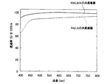
しかしながら、厳密かつ詳細に検討すると、最適化された条件で作成されたMPE有機EL素子構造は、電力変換効率においても相応の改善効果を実現できる。有機半導体は無機半導体に比べ電荷移動度が桁違いに低いため、所望の電流値を得るには「付加的な電圧」を要することは周知である。ここで言う「付加的な電圧」とは、例えば、2eVの光子を放出するのに最低限必要な2Vのデバイス電圧を超えて、単位時間当たり、所望の、多量の光子を放出するために必要な電流密度を得るために'付加的に'必要とされる電圧(つまり、この場合は(駆動電圧−2V)=(付加的電圧))を言う。したがって、一般的に、輝度が電流密度のみに比例する有機EL素子を例にとれば、輝度の高い領域での電力変換効率は輝度の低い領域での電力変換効率よりも低下する(図24参照)。しかしながら、MPE有機EL素子と従来の有機EL素子を同輝度において比較すれば、MPE素子の場合は所要電流密度が略1/(n+1)、(nは電荷発生層の層数)となり、そのとき各(単位)発光ユニット当たり、消費される電位は、従来の有機EL素子で消費される電位よりも低下するので、実際には全消費電力は低下することになる(つまり電力変換効率は上昇する)。図24に従来の有機EL素子構造を電荷発生層を介して2段(n=1)、5段(n=4)、10段(n=9)、と重ねた場合に、電力変換効率(lm/W)が各輝度ごとにどのように変化するかをシミュレートしたものを示した。ここでは電流効率(cd/A)がきっちり(n+1)倍となり、駆動電圧も、(同一輝度の時ではなく)同一電流密度の時に、きっちり(n+1)倍(nは電荷発生層の層数)となる場合を示している。因みに従来構造の有機EL素子のデータ(1段、n=0の場合)は実際に作製した素子のデータである。このような良好な状態のMPE素子は簡単に実現されるわけではない。例えば、所望の電流値を得るための電圧が従来構造の有機EL素子の(n+1)倍以上となる場合、つまり、発光ユニットを電荷発生層を介して重ねるたびに、望ましくない「過剰電圧(ΔV)」が加えられる事態が生じた場合は、当然のことながら電力変換効率も発光ユニットを重ねるたびに低下していくことになる。 However, when examined strictly and in detail, the MPE organic EL element structure prepared under optimized conditions can realize a corresponding improvement effect in power conversion efficiency. It is well known that an “additional voltage” is required to obtain a desired current value because an organic semiconductor has an order of magnitude lower charge mobility than an inorganic semiconductor. The “additional voltage” mentioned here means, for example, necessary to emit a desired large amount of photons per unit time exceeding the minimum device voltage of 2 V required to emit 2 eV photons. Is the voltage that is 'additionally' required to obtain the desired current density (ie (drive voltage -2V) = (additional voltage) in this case). Therefore, in general, when an organic EL element whose luminance is proportional only to the current density is taken as an example, the power conversion efficiency in the high luminance region is lower than the power conversion efficiency in the low luminance region (see FIG. 24). ). However, if the MPE organic EL element and the conventional organic EL element are compared at the same luminance, the required current density in the case of the MPE element is approximately 1 / (n + 1), where n is the number of charge generation layers. Since the potential consumed per (unit) light emitting unit is lower than the potential consumed by the conventional organic EL element, the total power consumption actually decreases (that is, the power conversion efficiency increases). ). In FIG. 24, when the conventional organic EL element structure is overlapped with two stages (n = 1), five stages (n = 4), and ten stages (n = 9) through the charge generation layer, the power conversion efficiency ( The simulation of how lm / W) changes for each luminance is shown. Here, the current efficiency (cd / A) is exactly (n + 1) times, and the drive voltage is exactly (n + 1) times (n is the number of charge generation layers) at the same current density (not the same luminance). Shows the case. Incidentally, the data of the organic EL element having the conventional structure (in the case of one stage, n = 0) is the data of the actually manufactured element. Such an MPE element in a good state is not easily realized. For example, when the voltage for obtaining a desired current value is not less than (n + 1) times that of an organic EL element having a conventional structure, that is, every time the light emitting units are stacked through the charge generation layer, an undesirable “excess voltage (ΔV ) ”Is added, it goes without saying that the power conversion efficiency decreases as the light emitting units are stacked.
図25、図26に、発光ユニットを2個有するMPE有機EL素子のバンド図を示した。望ましくない「過剰電圧(ΔV)」は電荷発生層部分内部(本発明における「ホール−電子変換層」内部)で発生する。そもそも有機EL素子におけるホールの発生(または、注入)とは電子供与性分子(ホール輸送性分子)のHOMO(最高占有軌道)準位の電子が引き抜かれた状態の生成、つまりラジカルカチオン分子の生成と同義である。したがってMPE素子における電荷発生層の役割とは、電圧印加時に、該ラジカルアニオン分子の生成に伴って引き抜かれた電子を別の(陽極側の)発光ユニットの電子受容性分子(電子輸送性分子)のLUMO(最低非占有軌道)準位に注入することである。したがって前述の「過剰電圧(ΔV)」は、該HOMO準位の電子が該LUMO準位に移動する際に存在する(「ホール−電子変換層」内部の)「エネルギー障壁」によって発生するものである。この「HOMO準位の電子がLUMO準位に移動する」ことを別言すれば、「ホール電流を電子電流に変換する」と、表わすことができる。したがって、(「ホール−電子変換層」内部の)該エネルギー障壁を限りなく0にすることで、(結果的に)「過剰電圧(ΔV)」を限りなく0にすることが出来たときに、前述の良好な状態のMPE有機EL素子を初めて実現出来ることになる(図26)。 25 and 26 show band diagrams of MPE organic EL elements having two light emitting units. An undesirable “excess voltage (ΔV)” is generated inside the charge generation layer portion (inside the “hole-electron conversion layer” in the present invention). In the first place, the generation (or injection) of holes in an organic EL element is the generation of a state in which electrons in the HOMO (highest occupied orbit) level of an electron donating molecule (hole transporting molecule) are extracted, that is, generation of a radical cation molecule. It is synonymous with. Therefore, the role of the charge generation layer in the MPE element is that, when a voltage is applied, electrons extracted with the generation of the radical anion molecule are separated from the electron-accepting molecule (electron-transporting molecule) of another (anode side) light-emitting unit. Is injected into the LUMO (lowest unoccupied orbital) level. Therefore, the “excess voltage (ΔV)” described above is generated by an “energy barrier” (inside the “hole-electron conversion layer”) that is present when electrons in the HOMO level move to the LUMO level. is there. In other words, “the HOMO level electrons move to the LUMO level” can be expressed as “converting the hole current into the electron current”. Therefore, when the energy barrier (inside the “hole-electron conversion layer”) is set to 0 as much as possible, (as a result) “excess voltage (ΔV)” can be set to 0 as much as possible, The above-mentioned MPE organic EL element in a good state can be realized for the first time (FIG. 26).
本発明者は鋭意検討の結果、該エネルギー障壁を限りなく0にして、理想的な「ホール電流−電子電流変換」を実現するに至った。具体的には、特開平11−233262号公報や特開2000−182774号公報(米国特許第6396209号明細書)(J.Endo,T.Matsumoto,and J.Kido,Jpn.J.Appl.Phys.Vol.41(2002)pp.L800−L803参照)で詳説されている手法を用いて、熱還元反応によって電子受容性有機物のラジカルアニオン分子が生成して存在している熱還元反応生成層と、特開平11−251067号公報や特開2001−244079号公報や特開2003−272860号等で詳説されている手法を用いて形成した層(遠藤ら、Jpn.J.Appl.Phys.Vol.41(2002)L358、第47回高分子学会予稿集、47巻9号、p1940(1998)、Leoら、Appl.Phys.Lett.、vol.78,No.4,(2001)参照)、つまり、酸化性分子によって、電子供与性有機物のラジカルカチオン分子が生成している層と、を順次重ねることによって、(HOMO準位を流れる)ホール電流が(LUMO準位を流れる)電子電流に障壁なく'変換'されることが判明した。 As a result of intensive studies, the present inventor has achieved the ideal “hole current-electron current conversion” by setting the energy barrier to 0 as much as possible. Specifically, JP-A-11-233262 and JP-A-2000-182774 (US Pat. No. 6,396,209) (J. Endo, T. Matsumoto, and J. Kido, Jpn. J. Appl. Phys.) Vol. 41 (2002) pp. L800-L803), a thermal reduction reaction product layer in which radical anion molecules of electron-accepting organic substances are generated by thermal reduction reaction and are present. A layer formed by using a method described in detail in JP-A-11-251067, JP-A-2001-244079, JP-A-2003-272860, etc. (Endo et al., Jpn. J. Appl. Phys. Vol. 41 (2002) L358, 47th Annual Meeting of the Polymer Society of Japan, 47 (9), p1940 (1998), Leo , Appl.Phys.Lett., Vol.78, No.4, (2001)), that is, by sequentially stacking a layer in which a radical cation molecule of an electron-donating organic substance is generated by an oxidizing molecule. It has been found that the hole current (flowing through the HOMO level) is 'converted' to the electron current (flowing through the LUMO level) without barrier.
しかしながら、本発明者らが開示した、特開平10−270171号公報(米国特許第6013384号明細書)、特開2001−102175号公報(米国特許第6589673号明細書)、J.Kido and T.Matsumoto,Appl.Phys.Lett.,73,p.2866(1998)、等で詳説されている手法、すなわち、アルカリ金属等の電子ドナー(還元性ドーパント)をドーピングすることで、電子受容性有機物のラジカルアニオン分子を生成した場合は、該電子ドナー(還元性ドーパント)と電子アクセプター(該酸化性分子)が直接に反応したり、前記電子受容性有機物と前記酸化性分子の間や、前記電子供与性分子(ホール輸送性分子)と前記電子ドナー(還元性ドーパント)の間にも、意図せずして、望ましくない反応が引き起こされ、結果として電子の移動を妨げることが懸念され、実際に本発明者の検討によれば該MPE有機EL素子の駆動電圧が段数(n+1)倍以上となってしまい、上記「過剰電圧(ΔV)」を0に出来ないことが判明した。ここで、「駆動電圧が発光ユニットの重ね段数倍以上となってしまい..」というのは、同電流密度(または、同輝度)を達成するための駆動電圧が発光ユニットの重ね段数倍以上となることを意味し、特に高電流密度(または、高輝度)領域になるにしたがってその傾向が顕著となる(つまりΔVの値には電流密度依存性がある)。このような望ましくない状態のMPE有機EL素子の実施例は、本発明者らによる特開2003−45676号公報や、特開2003−272860号公報に開示されている。
本発明の目的は、下記に記載する電子輸送部としての層とホール輸送部としての層の2つの層を連続して積層させた「ホール電流−電子電流変換層」(「ホール−電子変換層」)を、MPE有機EL素子の電荷発生層のみならず、従来型有機太陽電池を複数個、直列につなぐ「接続層」として用いたり、さらには一般的な有機素子の電極形成時のバッファー層として用いたりと、この層(が持つ利点)を一般化して広範囲に使用することで、従来型有機素子の持つ欠点を克服することにある。 An object of the present invention is to provide a “hole current-electron current conversion layer” (“hole-electron conversion layer”) in which two layers of an electron transport portion and a layer as a hole transport portion described below are successively laminated. )) As a “connection layer” connecting not only the charge generation layer of the MPE organic EL element but also a plurality of conventional organic solar cells in series, or a buffer layer for forming electrodes of general organic elements When this layer is used as a general purpose, this layer (advantages) is generalized and used over a wide range to overcome the disadvantages of conventional organic elements.
電子受容性有機物をラジカルアニオン分子とするために、(1)「アルカリ金属イオン、アルカリ土類金属イオン、希土類金属イオン、及び一部の遷移金属イオンを代表とする、仕事関数が4.0eV以下の低仕事関数金属のイオンのうち、少なくとも1種を含む化合物(有機物でも無機物でもよい)」と、「(アルミニウムのように)該化合物に含まれる金属イオンを真空中(例えば蒸着チャンバー内の雰囲気)で金属状態に還元しうる熱還元性金属」とを、(真空蒸着による)積層、もしくは、共蒸着による混合により接触させて反応させ、該熱還元反応によって還元された低仕事関数金属と、その近傍に存在する電子受容性有機物とを(電子の授受による)酸化還元反応によって電荷移動錯体を形成させて、該電子受容性有機物がラジカルアニオン状態にある電子輸送部(熱還元反応生成部)と、(2)(a)イオン化ポテンシャルが5.7eVより小さく、電子供与性すなわちホール輸送性を有する有機化合物と、(b)(a)の有機化合物と、(電子の授受による)酸化還元反応によって電荷移動錯体を形成しうる無機物質又は有機物質とが、積層、または混合されて接触しており、(a)の電子供与性有機物がラジカルカチオン状態にあるホール輸送部、とが積層されてなる「ホール電流−電子電流変換層」(「ホール−電子変換層」)を有していればよく、この層の使用法は特に限定されない。 In order to make an electron-accepting organic substance a radical anion molecule, (1) “work function is 4.0 eV or less, represented by“ alkali metal ions, alkaline earth metal ions, rare earth metal ions, and some transition metal ions ” A compound containing at least one kind of ions of a low work function metal (may be organic or inorganic) "and" (like aluminum) the metal ions contained in the compound are evacuated in a vacuum (for example, the atmosphere in the deposition chamber). And a low work function metal reduced by the thermal reduction reaction by contacting with a layer (by vacuum deposition) or by mixing by co-evaporation, A charge transfer complex is formed by an oxidation-reduction reaction (by transfer of electrons) with an electron-accepting organic substance present in the vicinity, and the electron-accepting organic substance is (B) (a) an electron transporting part (thermal reduction reaction generating part) in the state of luanion, (2) (a) an organic compound having an ionization potential smaller than 5.7 eV and having an electron donating property, that is, a hole transporting property; The organic compound of (a) is in contact with an inorganic substance or organic substance that can form a charge transfer complex by an oxidation-reduction reaction (by electron transfer), and the electron donating organic substance of (a) It is only necessary to have a “hole current-electron current conversion layer” (“hole-electron conversion layer”) formed by laminating a hole transport portion in a radical cation state, and the usage of this layer is not particularly limited. .
本発明の有機素子は、仕事関数が4.0eV以下の低仕事関数金属のイオンのうち少なくとも1種を含む有機金属錯体化合物と、有機金属錯体化合物中に含まれる金属イオンを真空中で金属状態に還元しうる熱還元性金属と、を積層もしくは共蒸着による混合により接触させて引き起こされたその場熱還元反応によって還元された低仕事関数金属と電子受容性有機物とが酸化還元反応によって電荷移動錯体を形成して、電子受容性有機物がラジカルアニオン状態にある電子輸送部、及び、イオン化ポテンシャルが5.7eVより小さく電子供与性を有する有機化合物と、有機化合物と酸化還元反応によって電荷移動錯体を形成しうる無機物質又は有機物質と、が積層または混合されて接触しており、電子供与性を有する有機物がラジカルカチオン状態にあるホール輸送部、が積層されてなるホール電流−電子電流変換層を含み、有機金属錯体化合物中で金属イオンに配位もしくは結合している有機分子部分が電子受容性有機物として機能することを特徴としている。 The organic element of the present invention comprises an organometallic complex compound containing at least one kind of ions of a low work function metal having a work function of 4.0 eV or less, and a metal ion contained in the organometallic complex compound in a metal state in a vacuum. Low-work-function metal reduced by in-situ thermal reduction reaction caused by contact with a heat-reducible metal that can be reduced to a layer or by mixing by co-evaporation, and an electron-accepting organic substance charge transfer by oxidation-reduction reaction Forming a complex, an electron transporting portion in which an electron-accepting organic substance is in a radical anion state, an organic compound having an ionization potential of less than 5.7 eV and an electron-donating property, and a charge transfer complex by an oxidation-reduction reaction with the organic compound. An inorganic substance or an organic substance that can be formed is laminated or mixed to be in contact, and an organic substance having an electron donating property is a radical catalyst. A hole current-electron current conversion layer formed by laminating a hole transport portion in an organic state, and an organic molecule portion coordinated or bonded to a metal ion in an organometallic complex compound functions as an electron-accepting organic substance. It is characterized by that.
本発明の有機素子は、電子輸送部と、ホール輸送部と、を積層してなるホール電流−電子電流変換層を含み、電子輸送部は、仕事関数が4.0eV以下の低仕事関数金属のイオンのうち少なくとも1種を含む有機金属錯体化合物と、有機金属錯体化合物に対して積層もしくは共蒸着による混合により接触し、有機金属錯体中に含まれる金属イオンを真空中で金属状態に還元しうる熱還元性金属と、を有し、接触により引き起こされたその場熱還元反応によって還元された低仕事関数金属と電子受容性有機物とが酸化還元反応によって電荷移動錯体を形成して、電子受容性有機物がラジカルアニオン状態にあり、ホール輸送層は、イオン化ポテンシャルが5.7eVより小さく電子供与性を有する有機化合物と、有機化合物に対して積層または混合されて接触し、有機化合物と酸化還元反応によって電荷移動錯体を形成しうる無機物質又は有機物質と、を有し、電子供与性を有する有機物がラジカルカチオン状態にあり、有機金属錯体化合物中で金属イオンに配位もしくは結合している有機分子部分が電子受容性有機物として機能することを特徴としている。 The organic element of the present invention includes a hole current-electron current conversion layer formed by laminating an electron transport portion and a hole transport portion, and the electron transport portion is made of a low work function metal having a work function of 4.0 eV or less. An organometallic complex compound containing at least one of the ions can be contacted with the organometallic complex compound by lamination or co-evaporation to reduce the metal ions contained in the organometallic complex to a metal state in a vacuum. A low-work function metal reduced by an in situ thermal reduction reaction caused by contact and an electron-accepting organic substance, forming a charge-transfer complex by an oxidation-reduction reaction, and accepting electrons The organic substance is in a radical anion state, and the hole transport layer is formed by stacking an organic compound having an ionization potential smaller than 5.7 eV and an electron donating property on the organic compound. An organic substance having an inorganic property or an organic substance capable of forming a charge transfer complex by an oxidation-reduction reaction with an organic compound, and having an electron-donating property in a radical cation state. The organic molecular part coordinated or bonded to the metal ion functions as an electron-accepting organic substance.
上記有機金属錯体化合物と電子受容性有機物は積層または混合されて接触していることが好ましい。 The organometallic complex compound and the electron-accepting organic material are preferably in contact with each other by being laminated or mixed.
上記有機金属錯体化合物と電子受容性有機物は、同一であっても良い。 The organometallic complex compound and the electron-accepting organic material may be the same.
上記熱還元性金属は、アルミニウム、ジルコニウム、シリコン、チタン及びタングステンから選択される少なくとも1種を含むことが望ましい。 The heat-reducible metal preferably includes at least one selected from aluminum, zirconium, silicon, titanium, and tungsten.
上記金属錯体化合物または上記無機化合物に含まれる低仕事関数金属のイオンがアルカリ金属イオンである場合は、上記熱還元性金属は、マグネシウム、カルシウム、ストロンチウム、及びバリウムのアルカリ土類金属から選択される少なくとも1種を含む金属であっても良い。 When the low work function metal ion contained in the metal complex compound or the inorganic compound is an alkali metal ion, the thermally reducible metal is selected from alkaline earth metals such as magnesium, calcium, strontium, and barium. A metal containing at least one kind may be used.
上記電子供与性有機化合物は、アリールアミン化合物であり、一般式(I): The electron donating organic compound is an arylamine compound, and is represented by the general formula (I):
上記電子供与性有機化合物は顔料型有機物であることが好ましい。 The electron donating organic compound is preferably a pigment organic material.
上記電子供与性有機化合物は、ポルフィリン化合物またはその誘導体であるとよい。 The electron donating organic compound may be a porphyrin compound or a derivative thereof.
上記電子供与性有機化合物は、キナクリドン化合物またはその誘導体であることが好ましい。 The electron donating organic compound is preferably a quinacridone compound or a derivative thereof.
上記電子供与性有機化合物は、インダンスレン化合物またはその誘導体であることが好ましい。 The electron donating organic compound is preferably an indanthrene compound or a derivative thereof.
上記電子供与性有機化合物は、ガラス転移点が90℃以上であるアリールアミン化合物であるとよい。 The electron donating organic compound is preferably an arylamine compound having a glass transition point of 90 ° C. or higher.
上記、電子供与性を有する有機化合物と酸化還元反応によって電荷移動錯体を形成しうる無機物質は、金属酸化物であることが好ましい。 The inorganic substance capable of forming a charge transfer complex by an oxidation-reduction reaction with an organic compound having an electron donating property is preferably a metal oxide.
上記、電子供与性を有する有機化合物と酸化還元反応によって電荷移動錯体を形成しうる無機物質は、金属ハロゲン化物であることが好ましい。 The inorganic substance capable of forming a charge transfer complex by an oxidation-reduction reaction with an organic compound having an electron donating property is preferably a metal halide.
上記、電子供与性を有する有機化合物と酸化還元反応によって電荷移動錯体を形成しうる金属酸化物は、V2O5(5酸化バナジウム)、7酸化2レニウム、MoO3(3酸化モリブデン)、又はWO3(3酸化タングステン)であることが好ましい。 The metal oxide that can form a charge transfer complex by an oxidation-reduction reaction with an organic compound having an electron donating property is V 2 O 5 (vanadium pentoxide), dirhenium 7 oxide, MoO 3 (molybdenum trioxide), or WO 3 (tungsten trioxide) is preferred.
上記電子供与性を有する有機化合物と酸化還元反応によって電荷移動錯体を形成しうる金属ハロゲン化物は、塩化第2鉄、臭化第2鉄、等の鉄ハロゲン化物や、アルミニウムハロゲン化物、ガリウムハロゲン化物、インジウムハロゲン化物、アンチモンハロゲン化物、又は、ヒ素ハロゲン化物から適宜選択されることが好ましい。 Metal halides capable of forming a charge transfer complex by an oxidation-reduction reaction with the above-mentioned electron-donating organic compound include iron halides such as ferric chloride and ferric bromide, aluminum halides, and gallium halides. Indium halide, antimony halide, or arsenic halide is preferably selected as appropriate.
上記、電子供与性を有する有機化合物と酸化還元反応によって電荷移動錯体を形成しうる有機物質は、少なくとも1個のフッ素を置換基として有するとよい。 The organic substance that can form a charge transfer complex by an oxidation-reduction reaction with an organic compound having an electron donating property preferably has at least one fluorine as a substituent.
上記、電子供与性を有する有機化合物と酸化還元反応によって電荷移動錯体を形成しうる有機物質は、少なくとも1個のシアノ基を置換基として有することが好ましい。 The organic substance capable of forming a charge transfer complex by an oxidation-reduction reaction with an organic compound having an electron donating property preferably has at least one cyano group as a substituent.
上記、電子供与性を有する有機化合物と酸化還元反応によって電荷移動錯体を形成しうる有機物質は、少なくとも1個のシアノ基と、少なくとも1個のフッ素を置換基として同時に有することが好ましい。 The organic substance capable of forming a charge transfer complex by an oxidation-reduction reaction with an organic compound having an electron donating property preferably has at least one cyano group and at least one fluorine as substituents at the same time.
上記、電子供与性を有する有機化合物と酸化還元反応によって電荷移動錯体を形成しうる有機物質は、テトラフルオロ−テトラシアノキノジメタンであることが好ましい。 The organic substance capable of forming a charge transfer complex by an oxidation-reduction reaction with an organic compound having an electron donating property is preferably tetrafluoro-tetracyanoquinodimethane.
上記、電子供与性を有する有機化合物と酸化還元反応によって電荷移動錯体を形成しうる有機物質は、少なくとも1個のホウ素原子を有していることが好ましい。 The organic substance capable of forming a charge transfer complex by an oxidation-reduction reaction with an organic compound having an electron donating property preferably has at least one boron atom.
上記、電子供与性を有する有機化合物と酸化還元反応によって電荷移動錯体を形成しうる有機物質は、少なくとも1個のホウ素原子と、少なくとも1個のフッ素を同時に有しているとよい。 The organic substance that can form a charge transfer complex by an oxidation-reduction reaction with an organic compound having an electron donating property preferably has at least one boron atom and at least one fluorine at the same time.
上記、電子供与性を有する有機化合物と酸化還元反応によって電荷移動錯体を形成しうる有機物質は、トリスβ−(ヘプタフルオロナフチル)ボランであるであることが好ましい。 The organic substance capable of forming a charge transfer complex by an oxidation-reduction reaction with an organic compound having an electron donating property is preferably tris β- (heptafluoronaphthyl) borane.
本発明の有機素子は、有機EL素子を含むことを特徴としている。 The organic element of the present invention includes an organic EL element.
本発明の有機素子は、有機太陽電池を含むことを特徴としている。 The organic element of the present invention includes an organic solar battery.
本発明の有機素子は、有機FET構造を含むことを特徴としている。 The organic element of the present invention is characterized by including an organic FET structure.
本発明の有機EL素子は、上記有機素子を含むことを特徴としている。 The organic EL device of the present invention is characterized by including the organic device.
本発明の有機太陽電池は、上記有機素子を含むことを特徴としている。 The organic solar cell of the present invention is characterized by including the organic element.
本発明の有機FET構造は、上記有機素子を含むことを特徴としている。 The organic FET structure of the present invention includes the organic element described above.
本発明の有機素子の製造方法は、仕事関数が4.0eV以下の低仕事関数金属のイオンのうち少なくとも1種を含む有機金属錯体化合物と、有機金属錯体化合物中に含まれる金属イオンを真空中で金属状態に還元しうる熱還元性金属と、を積層もしくは共蒸着による混合により接触させてその場熱還元反応を起こし、その場還元反応によって還元された低仕事関数金属と電子受容性有機物とを酸化還元反応によって電荷移動錯体を形成して、電子受容性有機物がラジカルアニオン状態にある電子輸送部を形成する工程と、イオン化ポテンシャルが5.7eVより小さく電子供与性を有する有機化合物と、有機化合物と酸化還元反応によって電荷移動錯体を形成しうる無機物質又は有機物質と、を積層または混合により接触させ、電子供与性を有する有機物がラジカルカチオン状態にあるホール輸送部を形成する工程と、を備えることを特徴としている。
本発明の有機素子の製造方法は、仕事関数が4.0eV以下の低仕事関数金属のイオンのうち少なくとも1種を含む無機化合物と、無機化合物中に含まれる金属イオンを真空中で金属状態に還元しうる熱還元性金属と、を積層もしくは共蒸着による混合により接触させてその場熱還元反応を起こし、その場還元反応によって還元された低仕事関数金属と電子受容性有機物とを酸化還元反応によって電荷移動錯体を形成して、電子受容性有機物がラジカルアニオン状態にある電子輸送部を形成する工程と、イオン化ポテンシャルが5.7eVより小さく電子供与性を有する有機化合物と、有機化合物と酸化還元反応によって電荷移動錯体を形成しうる無機物質又は有機物質と、を積層または混合により接触させ、電子供与性を有する有機物がラジカルカチオン状態にあるホール輸送部を形成する工程と、を備えることを特徴としている。
In the method for producing an organic element of the present invention, an organometallic complex compound containing at least one kind of ions of a low work function metal having a work function of 4.0 eV or less and a metal ion contained in the organometallic complex compound in vacuum The low work function metal and the electron-accepting organic substance reduced by the in-situ reduction reaction are brought into contact with a heat-reducible metal that can be reduced to a metal state by laminating or mixing by co-evaporation to cause in-situ thermal reduction reaction. Forming a charge transfer complex by an oxidation-reduction reaction to form an electron transporting portion in which an electron-accepting organic substance is in a radical anion state, an organic compound having an ionization potential of less than 5.7 eV, and an electron-donating property; The compound and an inorganic or organic substance capable of forming a charge transfer complex by an oxidation-reduction reaction are brought into contact with each other by stacking or mixing, and electron donating properties Organic substances is characterized by comprising a step of forming a hole-transporting unit in a radical cation state.
The method for producing an organic element of the present invention is a method in which an inorganic compound containing at least one kind of ions of a low work function metal having a work function of 4.0 eV or less and a metal ion contained in the inorganic compound are brought into a metal state in a vacuum. A heat-reducible metal that can be reduced is brought into contact by lamination or co-evaporation to cause an in-situ thermal reduction reaction, and a low work function metal reduced by the in-situ reduction reaction and an electron-accepting organic substance are oxidized and reduced. Forming a charge transfer complex to form an electron transport portion in which the electron-accepting organic substance is in a radical anion state, an organic compound having an ionization potential of less than 5.7 eV, an electron-donating property, an organic compound, and a redox An inorganic substance or an organic substance that can form a charge transfer complex by a reaction is brought into contact by lamination or mixing, and an organic substance having an electron-donating property is labeled. Forming a hole-transporting unit in the Karukachion state is characterized in that it comprises.
電子輸送部としての層とホール輸送部としての層を連続して積層させた「ホール電流−電子電流変換層」(「ホール−電子変換層」)を、MPE有機EL素子の電荷発生層のみならず、従来型有機太陽電池を複数個、直列につなぐ「接続層」として用いたり、さらには一般的な有機素子の電極形成時のバッファー層として用いたりと、この層(が持つ利点)を一般化して広範囲に使用することで、従来型有機素子の持つ欠点を克服することができる。 If the “hole current-electron current conversion layer” (“hole-electron conversion layer”), in which the layer as the electron transport portion and the layer as the hole transport portion are continuously laminated, is only the charge generation layer of the MPE organic EL device. First, it is used as a “connection layer” that connects multiple conventional organic solar cells in series, or as a buffer layer when forming electrodes for general organic elements. It is possible to overcome the disadvantages of the conventional organic element by using it in a wide range.
熱還元反応生成層(電子輸送部)中では、アルミニウムやマグネシウム等の熱還元性金属はすでに金属原子として存在しておらず、イオン状態(酸化状態)として存在しているため、下記の実施例に見られるように良好な透明性を付与することができる。アルカリ金属を代表とする還元性ドーパントは大気中で発火するほど反応活性なものがほとんどなので、本発明の手法はそのような金属のハンドリングが不要になる、という工程上の優位点がある。透明性が高く、かつ、発明者らが特開平10−270171号公報や特開2001−102175号公報等で開示した、還元性ドーパントがドーピングされた電子輸送層と略同等の比抵抗を有する膜を得ることが可能である。 In the thermal reduction reaction product layer (electron transport part), the thermally reducible metal such as aluminum or magnesium does not already exist as a metal atom but exists as an ionic state (oxidized state). As can be seen, good transparency can be imparted. Since most reducing dopants typified by alkali metals are reactive enough to ignite in the atmosphere, the method of the present invention has a process advantage that such metal handling is unnecessary. A film having high resistivity and having a specific resistance substantially equivalent to that of an electron transport layer doped with a reducing dopant disclosed by the inventors in Japanese Patent Laid-Open Nos. 10-270171 and 2001-102175 It is possible to obtain
<第1実施形態>
第1実施形態においては、電子輸送部(熱還元反応生成部)の構成物質として、アルカリ金属イオン、アルカリ土類金属イオン、希土類金属イオン及び一部の遷移金属イオンを代表とする仕事関数が4.0eV以下の低仕事関数金属(アルカリ金属)のイオン含有有機物として、
<First Embodiment>
In the first embodiment, the work function represented by alkali metal ions, alkaline earth metal ions, rare earth metal ions, and some transition metal ions is 4 as a constituent material of the electron transport unit (thermal reduction reaction generation unit). As an ion-containing organic substance of a low work function metal (alkali metal) of 0.0 eV or less,
このようにして生成した、熱還元反応生成層は(純粋な有機物と比べても)一般に、透明性が高く、さらに純粋な有機物と比べ比抵抗が低下する(つまり、導電性が上昇する)特徴がある。このような導電性の上昇は、該プロセスが「アルミニウムの様な金属を混入するプロセスであるから」、とする誤解を生ずることがあるが、上記のように、該熱還元反応生成層中では、既にアルミニウムは金属原子として存在しておらず、イオン状態(酸化状態)として存在している。したがって良好な透明性が付与される分けである。導電性の向上の要因は、上記Alq-(ラジカルアニオン)の生成に起因している(実施例4,5参照)。 The thermal reduction reaction product layer produced in this way is generally highly transparent (even compared to pure organic matter) and has a lower specific resistance (that is, increased conductivity) than pure organic matter. There is. Such an increase in conductivity may cause a misunderstanding that the process is “a process in which a metal such as aluminum is mixed”. However, as described above, in the thermal reduction reaction product layer, Already, aluminum does not exist as a metal atom but exists as an ionic state (oxidized state). Therefore, it is a division that imparts good transparency. The cause of the improvement in conductivity is due to the generation of Alq − (radical anion) (see Examples 4 and 5).
アルミニウム等の熱還元性金属の量はアルカリ金属イオン含有化合物中のイオンを金属に還元するための「過不足のない量」が好ましく、この量が少ないと十分に該熱還元反応を起こすことが出来ずに、結果として電子受容性(輸送性)有機物がラジカルアニオンとなることが出来ないし、過剰であると該熱還元反応に寄与出来ない(つまり酸化状態に変化出来ない)金属アルミニウムが残存するため、膜の透明性を低下させるので所望の効果が期待出来なくなる。このような現象を示す例を下記実施例4に示した。 The amount of the heat-reducible metal such as aluminum is preferably “amount that is not excessive or insufficient” for reducing the ions in the alkali metal ion-containing compound to the metal, and if this amount is small, the heat-reduction reaction may occur sufficiently. As a result, the electron-accepting (transporting) organic substance cannot be a radical anion, and if it is excessive, metallic aluminum that cannot contribute to the thermal reduction reaction (that is, cannot be changed to an oxidized state) remains. Therefore, since the transparency of the film is lowered, the desired effect cannot be expected. An example showing such a phenomenon is shown in Example 4 below.
<第2実施形態>
第2実施形態においては、電子輸送部(熱還元反応生成部)の構成物質として、第1実施形態と同様に低仕事関数金属(アルカリ金属)イオン含有化合物として、Liqの様なアルカリ金属イオン含有有機金属錯体と、Alqの様な電子受容性(輸送性)有機物と、さらにアルミニウムのような熱還元性金属を同時に蒸着して混合させて(3元共蒸着)、上記と同様の機能を持つ電子輸送部を作成することも可能である。この場合該3つの物質の蒸着比率を適正に制御することで、透明性が高く、かつ本発明者が特開平10−270171号公報や特開2001−102175号公報等で開示した還元性ドーパントがドーピングされた電子輸送層と略同等の比抵抗を有する膜を得ることが可能である(実施例5参照)。言うまでもなく、アルカリ金属を代表とする該還元性ドーパントは大気中で発火するほど反応活性なものがほとんどなので、本発明の手法はそのような金属のハンドリングが不要になる、という工程上の優位点がある。
Second Embodiment
In the second embodiment, as a constituent material of the electron transport part (thermal reduction reaction generation part), the low work function metal (alkali metal) ion-containing compound as in the first embodiment contains an alkali metal ion such as Liq. An organic metal complex, an electron-accepting (transporting) organic material such as Alq, and a thermally reducible metal such as aluminum are vapor-deposited and mixed at the same time (ternary co-evaporation) and have the same function as above. It is also possible to create an electron transport section. In this case, by appropriately controlling the deposition ratio of the three substances, the transparency is high, and the reducing dopant disclosed by the present inventor in JP-A-10-270171, JP-A-2001-102175, etc. It is possible to obtain a film having a specific resistance substantially equivalent to that of the doped electron transport layer (see Example 5). Needless to say, most of the reducing dopants typified by alkali metals are reactive so that they ignite in the atmosphere, so that the method of the present invention eliminates the need for handling such metals. There is.
<第3実施形態>
第3実施形態においては、電子輸送部(熱還元反応生成部)の構成物質として、
<Third Embodiment>
In the third embodiment, as a constituent material of the electron transport part (thermal reduction reaction generation part),
<第4実施形態>
第4実施形態においては、上記Liqの様に、アルカリ金属イオンを含有して、かつ、それ自身が電子受容性(輸送性)を併せ持つ化合物である場合は、熱還元性金属であるアルミニウムと適当な比率で同時に蒸着して混合させ(2元共蒸着)、上記と同様の機能を持つ電子輸送部を作成することも可能である。この場合は、アルミニウムによって熱還元されないLiqが残存していることが想定されており、酸化還元反応によって(Li+ + Liq-(ラジカルアニオン))の電荷移動錯体を形成する。もちろん、上記のアルカリ金属イオンや、希土類金属イオンのような低仕事関数金属のイオン含有化合物であれば、上記有機金属錯体に代えて無機化合物を使用してもよい。
<Fourth embodiment>
In the fourth embodiment, like Liq, when it is a compound that contains an alkali metal ion and also has an electron accepting property (transport property), it is appropriate to use aluminum that is a heat reducing metal. It is also possible to form an electron transport portion having the same function as described above by simultaneously depositing and mixing at a suitable ratio (binary co-deposition). In this case, it is assumed that Liq that is not thermally reduced by aluminum remains, and a charge transfer complex of (Li + + Liq − (radical anion)) is formed by an oxidation-reduction reaction. Of course, an inorganic compound may be used instead of the organometallic complex as long as it is an ion-containing compound of a low work function metal such as the alkali metal ion or rare earth metal ion.
上記の実施形態1〜4に示される電子輸送部に隣接して形成される本発明のホール輸送部は、既にこれまで有機EL素子のホール注入層やホール輸送層中で広く使用されている、イオン化ポテンシャルが5.7eVより小さく電子供与性を有する有機化合物と、前記有機化合物と酸化還元反応によって電荷移動錯体を形成しうる無機物質又は有機物質と、が積層または混合されて接触しており、前記電子供与性を有する有機化合物がラジカルカチオン状態にあるホール輸送部となっている。
The hole transport part of the present invention formed adjacent to the electron transport part shown in the
なお、有機化合物、金属、及び「ホール電流−電子電流変換層」の成膜には、日本ビーテック製真空蒸着機を使用した。蒸着物質の成膜速度の制御や膜厚の制御は該蒸着機に取付けられている、水晶振動子を使用した成膜モニターCRTM−8000(ULVAC(日本真空技術社)製)を使用した。また、成膜後の実質膜厚の測定には、テンコール(Tencor)社製P10触針式段差計を用いた。素子の特性評価には、ケースレー(KEITHLEY)社ソースメータ2400、トプコンBM−8輝度計を使用した。また、吸収スペクトルの測定は、パーキンエルマー製:ラムダ19を使用して測定した。 In addition, the vacuum deposition machine made from Japan B-Tech was used for film-forming of an organic compound, a metal, and a "hole current-electron current conversion layer". A film formation monitor CRTM-8000 (manufactured by ULVAC (Nippon Vacuum Technology Co., Ltd.)) using a crystal resonator, which is attached to the vapor deposition machine, was used for the control of the deposition rate and the film thickness of the vapor deposition material. In addition, a P10 stylus type step gauge manufactured by Tencor was used for measurement of the actual film thickness after film formation. For the device characteristic evaluation, a Keithley source meter 2400 and a Topcon BM-8 luminance meter were used. Further, the absorption spectrum was measured using a lambda 19 manufactured by PerkinElmer.
以下に実施例を挙げて本発明をさらに詳細に説明するが、本発明はこれにより限定されるものではない。 The present invention will be described in more detail with reference to examples below, but the present invention is not limited thereto.
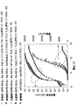
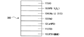
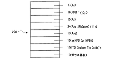
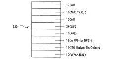
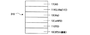
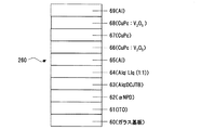
実施例1は、陰極に接する層に、本発明の「ホール電流−電子電流変換層」を有しており、結果的に、ホール電流の流れる層が陰極に接している有機EL素子の例である。この例では、図1に示すように、ガラス基板10上にパターニングされたITO(Indium Tin Oxide)陽極11上に、下記式
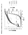
次に、上記AlqとLiq(低仕事関数金属イオン含有化合物)を、モル比率1:1で50Åの厚さに成膜した(層14)。さらにその上から熱還元性金属であるアルミニウムを15Å(に相当する量)蒸着した(層15)。次に上記αNPDと5酸化バナジウム(V2O5)をモル比率1:1で100Åの厚さで成膜した(層16)(ホール輸送部)。最後に陰極金属17としてアルミニウムを1000Åの厚さで成膜した。この有機EL素子210の構造を簡便に表記すると、ITO/αNPD(600Å)/Alq(600Å)/Alq:Liq(1:1)(50Å)/Al(15Å)/V2O5:αNPD(1:1)(100Å)/Al (図1)となる。以下の説明ではこのような(簡便な)表記法を用いることとする。この有機EL素子210において、陽極電極であるITOと陰極電極であるAlとの間に、直流電圧を印加して、諸特性を測定した結果を図3に示す。図3の○プロットは、この素子の電圧(V)−電流密度(mA/cm2)−輝度(cd/m2)特性を示す。また、この素子の動作概念を示した図2に示すように、層14及び層15は、電子輸送部(熱還元反応生成層)18として、層16と層18はホール電流−電子電流変換層19として機能する。
<比較例1>
比較例1は、実施例1と比較するため、本発明の電子輸送部である熱還元反応生成層18を用いない構造、すなわち、実施例1の層14のLiqに代えて金属Liを層104に使用した例であり、その素子300の構造はITO/αNPD(600Å)/Alq(600Å)/Alq:Li(1:1)(50Å)/V2O5:αNPD(1:1)(100Å)/Al (図4)となっている。この有機EL素子300の諸特性を測定した結果を図3の●プロットで示す。
Next, the Alq and Liq (low work function metal ion-containing compound) were formed in a molar ratio of 1: 1 to a thickness of 50 mm (layer 14). Further, aluminum, which is a heat-reducible metal, was vapor-deposited (corresponding to 15) (layer 15) thereon. Next, αNPD and vanadium pentoxide (V 2 O 5 ) were formed at a molar ratio of 1: 1 to a thickness of 100 mm (layer 16) (hole transport portion). Finally, aluminum was deposited as a
<Comparative Example 1>
In Comparative Example 1, for comparison with Example 1, a structure in which the thermal reduction reaction product layer 18 which is an electron transport portion of the present invention is not used, that is, instead of Liq of the
実施例2においては、実施例1の層14のLiqに代えて、
実施例3においては、実施例1の層14のLiqに代えてアルカリ金属の無機化合物であるLiF(フッ化リチウム)を層34に使用して、 ITO/αNPD(600Å)/Alq(600Å)/LiF(10Å)/Al(15Å)/V2O5:αNPD、(100Å)/Al (図6)なる構造の素子230を作成した。この構造は電子受容性化合物であるAlq(層13)とアルカリ金属化合物のLiF(層34)が、(混合ではなく)積層されて接触している。この有機EL素子230の諸特性を測定した結果を図3の△プロットで示す。
<参考例1> (従来型の有機EL素子の例)
参考例1として、本発明の「ホール電流−電子電流変換層」の構成を有していない、すなわち実施例1の層14〜16を有さない素子310を作成した。この素子は、実施例1の層14〜16に代えて、Alq:Li(1:1)からなる層114を備えており、ITO/αNPD(600Å)/Alq(600Å)/Alq:Li(1:1)(50Å)/Alなる構造となっている(図7)。この有機EL素子の諸特性を測定した結果を図3の◆プロットで示す。実施例1〜3、比較例1、参考例1の結果を比較すると、本発明の「ホール電流−電子電流変換層」を有する有機EL素子は従来型の素子と比べても遜色なく機能し、むしろ、より低電圧で駆動出来ることが分かった。また、アルカリ金属のような還元性ドーパントを使用すると、ホール電流−電子電流変換層内部に、エネルギー障壁が生成してしまうため、同電流密度、または同輝度を達成するために必要な電圧が高くなることが示された。
In Example 3, LiF (lithium fluoride), which is an alkali metal inorganic compound, was used for the
<Reference Example 1> (Example of conventional organic EL element)
As Reference Example 1, an
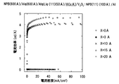
実施例4として、熱還元性金属の役割を確認し、かつ、その最適蒸着量(もしくは最適膜厚)を確認する実験を行った。実施例1の構造を基準にして、熱還元性金属であるアルミニウムの蒸着量を変化させて、有機EL素子としての特性の変化を調べた。すなわちITO/αNPD(600Å)/Alq(600Å)/Alq:Liq(1:1)(50Å)/Al(XÅ)/V2O5:αNPD(1:1)(100Å)/Alの構造で、Alの層15の膜厚(XÅ)を変化させた。
As Example 4, an experiment was conducted to confirm the role of the thermally reducible metal and to confirm the optimum deposition amount (or optimum film thickness). Using the structure of Example 1 as a reference, the amount of deposition of aluminum, which is a heat-reducible metal, was changed, and changes in characteristics as an organic EL element were examined. That is, the structure of ITO / αNPD (600 Å) / Alq (600 Å) / Alq: Liq (1: 1) (50 Å) / Al (XV) / V 2 O 5 : αNPD (1: 1) (100 Å) / Al, The film thickness (XÅ) of the
図8、図9の▽プロットはX=0(つまりアルミニウムを蒸着しない場合)のとき、◆プロットはx=3Åのとき、×プロットはX=10Åのとき、○プロットはX=15Åのとき、△プロットはX=20Åのときの各素子の、電圧(V)−電流密度(mA/cm2)−輝度(cd/m2)特性(図8)、電流密度(mA/cm2)−電流効率(cd/A)(図9)を示す。この結果から、熱還元性金属の蒸着量が所定量より少ないと、発光が観測されないことが示された(x=0Å,もしくは3Åの場合に対応)。これは、熱還元反応生成層内で電子受容性有機物のラジカルアニオン分子が生成されなかったため、発光層内に電子が注入されなかったためである。したがって、この時観測された電流はホール電流のみの電流である(2.2V近辺に発光開始電圧を示唆する'キンク(Kink)'が観測されないという事実からも、そのことが裏付けられる。)。また、図8、図9のグラフに示される結果から、この実験の範囲内ではアルミニウムを15Åの膜厚に相当する量に制御すると、輝度や効率が最も高い値を示すことが分かった。それ以上にアルミニウムの蒸着量を増やすと、熱還元反応に寄与しない(つまり酸化状態に変化出来ない)金属アルミニウムが残存して素子特性を低下させることが示された。 8 and 9, the ▽ plot is when X = 0 (that is, when aluminum is not deposited), the ◆ plot is when x = 3 mm, the X plot is when X = 10 mm, the ◯ plot is when X = 15 mm, Δ plot shows voltage (V) -current density (mA / cm 2 ) -luminance (cd / m 2 ) characteristics (FIG. 8), current density (mA / cm 2 ) -current of each element when X = 20 Å. Efficiency (cd / A) (FIG. 9) is shown. From this result, it was shown that no luminescence was observed when the deposition amount of the thermally reducible metal was less than a predetermined amount (corresponding to the case of x = 0 = or 3Å). This is because electrons were not injected into the light emitting layer because the radical anion molecule of the electron accepting organic material was not generated in the thermal reduction reaction product layer. Therefore, the current observed at this time is only the Hall current (this is supported by the fact that no “kink” suggesting the light emission starting voltage is observed in the vicinity of 2.2 V). Further, from the results shown in the graphs of FIGS. 8 and 9, it was found that the brightness and the efficiency were the highest when aluminum was controlled to an amount corresponding to a film thickness of 15 mm within the range of this experiment. It has been shown that when the amount of aluminum deposited is further increased, metallic aluminum that does not contribute to the thermal reduction reaction (that is, cannot be changed to an oxidized state) remains and deteriorates the device characteristics.
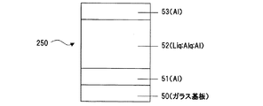
実施例5は、低仕事関数金属のイオン含有化合物と、電子受容性有機物と、熱還元性金属を同時に蒸着(3元共蒸着)して「透明性」と「導電性」を付与させた例である。Alがパターニングされたガラス基板50と、吸光度測定用の石英基板56をそれぞれ用意して、以下の手順で蒸着成膜を行った。 Example 5 is an example in which “transparency” and “conductivity” are imparted by simultaneously vapor-depositing (ternary co-deposition) an ion-containing compound of a low work function metal, an electron-accepting organic substance, and a heat-reducing metal. It is. A glass substrate 50 patterned with Al and a quartz substrate 56 for measuring absorbance were prepared, and vapor deposition was performed in the following procedure.
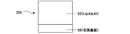
まず、低仕事関数有機金属錯体であるLiqと、電子受容性有機物であるAlqと、熱還元性金属であるAl(アルミニウム)を、Al電極51上に、膜厚速度比で、(Liq:Alq:Al=1Å/s(Liq):3Å/s(Alq):0.3Å/s(Al))となるように共蒸着して層52を形成し、さらにAl電極53を生成し、Al/Liq:Alq:Al/Al (図10)の構造の素子250を作成した。
First, Liq, which is a low work function organometallic complex, Alq, which is an electron-accepting organic substance, and Al (aluminum), which is a heat-reducing metal, are placed on the
また、比較用素子として、上記層52に代えて、アルカリ金属としてLiを直接電子受容性有機物(Alq)と混合して層54を生成した、Al/Alq:Li(1:1,モル比率)/Al(図11)の構造の素子251を作成した。
In addition, as a comparative element, instead of the
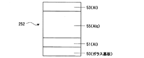
また、上記層52に代えて、Alq単独膜55を電極51、53で挟んだ、Al/Alq/Al (図12)の構造の素子252を作成して、それぞれ、電場(V/cm)−電流密度(A/cm2)特性を測定した(図15)。
In addition, instead of the
図15のグラフに示される通り、(Al/Liq:Alq:Al/Al)(図10)の構造の素子と、(Al/Alq:Li(1:1,モル比率)/Al)(図11)の構造の素子は、略同等の特性を示し、〜109Ωcmの比抵抗を示すことが分かった。これはAlによってLiq中のLiイオンが熱還元反応によって金属に還元され、ついで還元されたLi金属が電子受容性有機物である、Alqと電子の授受(酸化還元反応)によって電荷移動錯体(Li++Alq-(ラジカルアニオン))を形成したことを示している。 As shown in the graph of FIG. 15, an element having a structure of (Al / Liq: Alq: Al / Al) (FIG. 10) and (Al / Alq: Li (1: 1, molar ratio) / Al) (FIG. 11). It was found that the element having the structure of) exhibited substantially the same characteristics and a specific resistance of 10 9 Ωcm. This is reduced to the metal by a Li-ion thermal reduction reaction in Liq by Al, then reduced Li metal is an electron-accepting organic charge transfer complex upon Alq and electron transfer (redox reaction) (Li + + Alq − (radical anion)).
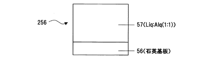
また、吸光度(及び、透過率)測定用素子として、石英基板56上にLiq:Alq:Alを共蒸着して 石英基板/Liq:Alq:Al、(図13)なる構造の素子255を作成した。この素子255は、石英基板56上に、膜厚速度比で、(Liq:Alq:Al=1Å/s(Liq):3Å/s(Alq):0.3Å/s(Al))となるように共蒸着して層52を形成した。また、比較用素子256として、熱還元性金属であるAlを混入させずに、石英基板56上にLiq:Alq(層57)を共蒸着して石英基板/Liq:Alq の素子を作成した。(図14)
図16は、上記吸光度測定用素子(図13)と比較用素子(図14)について、層52(Liq:Alq:Al)及び層57(Liq:Alq)を1000Åとしたときの波長(nm)−透過率(%)特性を測定した結果を示している。図16に示されるとおり、本発明の電子輸送部である(Liq:Alq:Al)(層52)からなる混合膜は、有機物のみからなる(Liq:Alq)(層57)と比べて、同じ膜厚(1000Å)当たりの透過率が大きく上昇することが確かめられた。また、本発明者は、前出の論文誌Appl.Phys.Lett.、73、p.2866(1998)中でリチウム金属ドーピング膜の吸収スペクトルの変化を示しているが、図17に示されるとおり、本発明の、(石英基板/Liq:Alq:Al)(吸光度測定用素子(図13))の吸収スペクトルと(石英基板/Liq:Alq)(比較用素子(図14))の吸収スペクトルの変化は、該論文中に示されている吸収スペクトルの変化と酷似しており、さらに、成膜時に金属アルミニウムを混入しているにもかかわらず、透明性が増してることからも、上記の熱還元反応と、引き続いて起こっている酸化還元反応による電荷移動錯体の形成をしめすことが分かる。
Further, as an element for measuring absorbance (and transmittance), Liq: Alq: Al was co-evaporated on the quartz substrate 56 to produce an
FIG. 16 shows the wavelength (nm) when the layer 52 (Liq: Alq: Al) and the layer 57 (Liq: Alq) are 1000 mm for the absorbance measuring element (FIG. 13) and the comparative element (FIG. 14). -The result of measuring the transmittance (%) characteristic is shown. As shown in FIG. 16, the mixed film made of (Liq: Alq: Al) (layer 52), which is the electron transport portion of the present invention, is the same as (Liq: Alq) (layer 57) made of only organic matter. It was confirmed that the transmittance per film thickness (1000 mm) greatly increased. In addition, the inventor of the present invention described in the above-mentioned paper journal Appl. Phys. Lett. 73, p. 2866 (1998) shows the change of the absorption spectrum of the lithium metal doping film. As shown in FIG. 17, (Quartz substrate / Liq: Alq: Al) (absorbance measuring element (FIG. 13 )) And the change in absorption spectrum of (quartz substrate / Liq: Alq) (comparative element (FIG. 14)) are very similar to the change in absorption spectrum shown in the paper, Despite the inclusion of metallic aluminum during film formation, transparency increases, indicating that the above-mentioned thermal reduction reaction and the subsequent oxidation-reduction reaction form a charge transfer complex. .
実施例6は、本発明の有機素子を無反射膜へ適用した例である。
着色顔料であって、かつ、ホール輸送能力を有することが知られている、
It is a color pigment and is known to have a hole transport capability.
図18に示すように、ガラス基板60上にITO層61、αNPD層62、赤色発光層63(DCJTB:Alq)の順に形成した有機EL素子構造の上に、Alq:Liq(1:1)からなる層64、Alからなる層65、V2O5:CuPcからなる層66を順に積層してなる本発明の「ホール電流−電子電流変換層」を形成し、さらにその上にCuPcの層67を積層する。また、このCuPcの層67の上に、CuPc:V2O5の層68及びAlの層(陰極)69を形成してITO/αNPD/DCJTB:Alq/Alq:Liq(1:1)(50Å)/Al(15Å)/V2O5:CuPc/CuPc/V2O5:CuPc/Al (図18)の構造の素子260を生成する。
As shown in FIG. 18, on the organic EL element structure formed on the
ここで(DCJTB:Alq)の発光層63で発生した赤色光のうち、陰極69であるAl方向に進行する光は(CuPc/V2O5:CuPc)の膜厚を調整して吸収させることが出来るので、コントラスト比の高い素子260を作成することが出来る。また、「第39回応用物理学関係連合講演会講演予稿集、28p−Q−9,p.1036(1992)」に記載されているキナクリドン顔料とその誘導体や、特開2000−58267号公報に記載されているインダンスレン顔料等、ホール輸送性を有して、かつ、特有の波長域に光吸収能を有する場合は、本発明の構造を利用して、単独、もしくは積層や混合の方法で、適宜、光反射陰極に接するホール電流層として利用出来る。このような顔料タイプの有機分子はホール輸送性である場合がほとんどなので、通常の有機EL素子の様に陰極に接する層に電子輸送性物質が必須である場合は、(言うまでもないが)このような顔料タイプのホール輸送性有機物を使用出来ない。
Of the red light generated in the light-emitting
実施例7は、本発明の有機素子を高エネルギー成膜時のダメージ低減層へ適用した例である。 Example 7 is an example in which the organic element of the present invention is applied to a damage reduction layer during high energy film formation.
有機EL素子の陰極形成法として電子ビーム蒸着やスパッタリング蒸着等の高エネルギー粒子堆積法を用いるアイディアが知られている。本発明者は、前出の金属ドーピング層を電子注入層として用いれば、高仕事関数を有するITOでも容易に電子注入出来ることを、特開2002−332567号公報(特願2001−142672号明細書)に記載した。この時用いられたスパッタリング装置は有機膜に損傷のない工夫が施されているが、厳密には依然、若干のダメージが観測されていた。また、特開2000−58265号公報や特開2000−68063号公報には発光層上に銅フタロシアニン(CuPc)層をスパッタバッファー層として形成するアイディアが記されている。そこではLi等のアルカリ金属を、薄く形成されたCuPc上に蒸着すると、該Li金属はCuPc層中に拡散して発光層方向に横切ることが記されており、この場合は、結果的に、CuPcは(ホール輸送性分子としてではなく)電子輸送性分子としても作用できることが開示されている。しかし、本来CuPcはホール輸送性分子であり、このように電子輸送層として使用する方法には素子の劣化を早める要因となる懸念が生じる。 An idea using a high energy particle deposition method such as electron beam vapor deposition or sputtering vapor deposition is known as a method for forming a cathode of an organic EL element. The present inventor has disclosed that if the metal doping layer described above is used as an electron injection layer, it is possible to easily inject electrons even with ITO having a high work function (Japanese Patent Application No. 2002-132672). ). The sputtering apparatus used at this time was devised so as not to damage the organic film, but strictly speaking, some damage was still observed. Japanese Patent Application Laid-Open Nos. 2000-58265 and 2000-68063 describe ideas for forming a copper phthalocyanine (CuPc) layer as a sputtering buffer layer on a light emitting layer. There, it is described that when an alkali metal such as Li is deposited on CuPc formed thinly, the Li metal diffuses into the CuPc layer and crosses in the direction of the light emitting layer. In this case, as a result, It is disclosed that CuPc can also act as an electron transport molecule (not as a hole transport molecule). However, CuPc is originally a hole transporting molecule, and there is a concern that the method of using it as an electron transporting layer becomes a factor that accelerates the deterioration of the device.
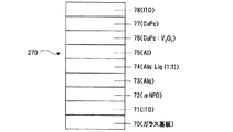
一方、本発明の「ホール電流−電子電流変換層」を用いれば、スパッタ等の高エネルギー粒子堆積時のバッファー層としてのCuPcは従来通り、(本来の性質である)ホール輸送層として機能させることが出来る。例えば、ガラス基板70上に、ITOの層71、αNPDの層72、Alqの層73、Alq:Liq(1:1)の層74、Al層75、V2O5:CuPcの層76、CuPcの層77及びAl、ITOまたはその他の材料からなる陰極78を積層してITO/αNPD/Alq/Alq:Liq(1:1)(50Å)/Al(15Å)/V2O5:CuPc/CuPc/陰極(Al,ITO,etc) (図19)の構造の素子270を生成できる。
On the other hand, if the “hole current-electron current conversion layer” of the present invention is used, CuPc as a buffer layer at the time of high energy particle deposition such as sputtering can function as a hole transport layer (which is an original property) as usual. I can do it. For example, on a glass substrate 70, an
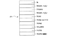
また、図19に示す上記素子の層77の上に、V2O5:CuPcの層79を形成してITO/αNPD/Alq/Alq:Liq(1:1)、50Å/Al、15Å/V2O5:CuPc/CuPc/V2O5:CuPc/陰極(Al,ITO,etc) (図20)の様な構造を有する素子271を生成できる。これらの素子270、271によって、本来のホール輸送層としての機能と高エネルギー粒子によるダメージ低減層としての機能を併せ持つことが出来る。
Further, a layer 79 of V 2 O 5 : CuPc is formed on the
実施例8は、本発明の有機素子を有機太陽電池への適用例である。有機太陽電池素子は有機EL素子と似た構造を有しており、特に二層型タイプは、(ホール輸送性分子/電子輸送性分子)の界面で、光によって電荷発生することが知られている。例えば、
1)Appl.Phys.Lett.、48,183(1986)
2)Chemistry Letters, pp.327−330(1990)
3)Appl.Phys.Lett.、76,2650(2000)
4)Appl.Phys.Lett.、79,126(2001)
5)Appl.Phys.Lett.、80,1667(2002)
に記載されている、典型的な構造が知られている。
特に、上記の、2)や5)の文献では、従来の有機太陽電池の両電極に挟まれた部分(電荷発生ユニット)が複数個、直列に接続された構造が記載されており、例えば、5)の文献中では、ITO/CuPc/PTCBI/Ag/CuPc/PTCBI/Agという、極薄(5Å)のAg(銀)を使用して、電荷発生ユニット(CuPc/PTCBI)を2個直列に連結する構造がしめされている。この極薄のAgの代わりに、本発明の「ホール電流−電子電流変換層」を使用することが出来る。つまり、例えばITO/CuPc/PTCBI/PTCBI:Rb(DPM):Alの共蒸着層/V2O5:CuPcの共蒸着層/CuPc/PTCBI/Agという構造によって、透明性が高く、かつ純粋な有機膜と比べても低抵抗化した膜であって、かつ、2個の電荷発生ユニットを、あたかも直列に接続できて、開放端電圧を略2倍とすることが出来る。上記の「PTCBI:Rb(DPM):Alの共蒸着層/V2O5:CuPcの共蒸着層」が本発明の「ホール電流−電子電流変換層」として作用する。そのほか、ITO/((アリールアミン化合物等の)電子供与性(ホール輸送性)有機物):(V2O5や、4F−TCNQ等)/CuPc/PTCBI/((電子受容性(輸送性)有機物:低仕事関数金属のイオン含有化合物:熱還元性金属)の反応生成層)/((アリールアミン化合物等の)電子供与性(ホール輸送性)有機物):(V2O5や、4F−TCNQ等)の共蒸着膜/CuPc/PTCBI/((電子受容性(輸送性)有機物:低仕事関数金属のイオン含有化合物:熱還元性金属)の反応生成層)/金属の様に、従来から知られている、「電荷発生ユニット」の構成をそのまま使用して、該「電荷発生ユニット」を複数個、直列に接続できる。ここで、アミールアミンは、
Example 8 is an application example of the organic element of the present invention to an organic solar cell. The organic solar cell element has a structure similar to that of an organic EL element, and in particular, the two-layer type is known to generate charges by light at the (hole transport molecule / electron transport molecule) interface. Yes. For example,
1) Appl. Phys. Lett. 48, 183 (1986)
2) Chemistry Letters, pp. 327-330 (1990)
3) Appl. Phys. Lett. 76, 2650 (2000)
4) Appl. Phys. Lett. 79, 126 (2001)
5) Appl. Phys. Lett. , 80, 1667 (2002)
The typical structure described in is known.
In particular, the above references 2) and 5) describe a structure in which a plurality of portions (charge generation units) sandwiched between both electrodes of a conventional organic solar cell are connected in series. 5) In the literature, ITO / CuPc / PTCBI / Ag / CuPc / PTCBI / Ag, using ultra-thin (5 mm) Ag (silver), two charge generation units (CuPc / PTCBI) are connected in series. The structure to connect is shown. Instead of this ultra-thin Ag, the “hole current-electron current conversion layer” of the present invention can be used. That is, for example, ITO / CuPc / PTCBI / PTCBI: Rb (DPM): Al co-deposited layer / V 2 O 5 : CuPc co-deposited layer / CuPc / PTCBI / Ag is highly transparent and pure. Compared to the organic film, the film has a reduced resistance, and two charge generation units can be connected in series, so that the open-circuit voltage can be approximately doubled. The above-described “PTCBI: Rb (DPM): Al co-deposited layer / V 2 O 5 : CuPc co-deposited layer” acts as the “Hall current-electron current conversion layer” of the present invention. In addition, ITO / (electron donating (hole transporting property) organic substance (such as arylamine compound)): (V 2 O 5 , 4F-TCNQ, etc.) / CuPc / PTCBI / ((electron accepting (transporting) organic substance) : Reaction product layer of ion-containing compound of low work function metal: thermoreducible metal) / (electron donating (hole transporting) organic substance (such as arylamine compound)): (V 2 O 5 or 4F-TCNQ Etc.) co-deposited film / CuPc / PTCBI / (reaction product layer of (electron-accepting (transporting) organic substance: ion-containing compound of low work function metal: heat-reducing metal)) / metal A plurality of the “charge generation units” can be connected in series by using the configuration of the “charge generation unit” as it is. Here, amyramine is
「電荷発生ユニット」の構成自体は、本発明の要素ではなく、既知のものや、新規に発見された好適な構成であれば、適宜用いることが出来る。なお、例えば、特開2003−264085号公報には、本発明と類似の構造で、上記文献1)に記載されている「電荷発生ユニット」の構成を用いて、ITO/CuPc/PV/CuPc:PVの共蒸着膜/CuPc/PV/Auという構造が、開示されており、このような構造でも、あたかも、開放端電圧を2倍にすることが可能であるかのように記載されているが、本発明者の検討では、2倍はおろか、「電荷発生ユニット」が1個の素子よりも発生電圧が低下することが明らかになった。これは、同一の物質の組み合わせを使用しても、積層膜構造(CuPc/PV)と混合膜構造(CuPc:PVの共蒸着膜)の相違の様な、態様の相違によって、「光電荷の発生機能」や「(電荷移動錯体の形成による)導電性の発現」という互いに別事象の機能が起こりうる、という「間違った期待」から記載されている。しかし、実際には、本発明の「ホール電流−電子電流変換層」のような機能がなければ、期待される機能を得ることは出来ない。
The configuration itself of the “charge generation unit” is not an element of the present invention, and any known configuration or a newly discovered suitable configuration can be used as appropriate. For example, in Japanese Patent Application Laid-Open No. 2003-264085, ITO / CuPc / PV / CuPc: which has a structure similar to that of the present invention and uses the structure of “charge generation unit” described in the above-mentioned document 1): A structure of PV co-deposited film / CuPc / PV / Au is disclosed, and even with such a structure, it is described as if the open-circuit voltage can be doubled. As a result of investigation by the present inventor, it has been clarified that the generated voltage of the “charge generating unit” is lower than that of one element, as well as twice. This is because even if the same combination of materials is used, depending on the difference in mode, such as the difference between the laminated film structure (CuPc / PV) and the mixed film structure (CuPc: PV co-deposited film), It is described from “wrong expectation” that functions of different events such as “generation function” and “conductivity development (by formation of charge transfer complex)” can occur. However, in reality, if there is no function like the “Hall current-electron current conversion layer” of the present invention, the expected function cannot be obtained.
実施例9は、本発明の有機素子を有機ELトランジスタへ適用した例である。
SIT(Static Induction Transistor)と呼ばれている、縦型FET(Field Effect Transistor)構造を有する有機ELトランジスタが知られている。(第47回応用物理学関係連合講演会 講演予稿集30a−H−2,p.1297、第63回応用物理学関係連合講演会 講演予稿集29p−ZH−15,p.1161) このような有機ELトランジスタの例として、図21に示すような素子320があり、基板90上に、順に、透明電極(ソース)91、ホール注入層92、ホール輸送層93、発光層94、陰極(ドレイン)95を形成してなる有機EL素子のホール輸送層93部分にスリット状のゲート電極(G)96が埋め込まれた形状を有しており、ゲート電極に印加される可変電圧値によって、発光閾値電圧や、発光強度を制御できる。しかし、(図21に示される通り)この構造によると、光の進行が妨げられたり、該ゲート電極のスリット間隔を自由に最適化することが難しくなる。これに対して、本発明の「ホール電流−電子電流変換層」を用いることで、従来の有機ELトランジスタ構造では実現できなかった構造も実現可能となる。例えば陰極95に接する層として、ホール輸送層97を配置することが出来る(図22)。このとき、陰極95とホール輸送層97との間には、例えばV2O5(電子受容性化合物)とNPB(電子供与性有機物)からなるホール輸送部98を生成することができ、発光層94とホール輸送層97との間に本発明のホール電流−電子電流変換層120を形成するホール輸送部99と電子輸送部100を生成することができる。このような構成の有機ELトランジスタ290においては、該ホール輸送層97部分にスリット状ゲート電極96を埋め込んで、従来の有機EL素子部分の構造を変えることなく、トランジスタ特性を付与出来る。また、例えば、陽極91に接する層として、電子輸送層121を配置することが出来る(図23)。このとき、陽極91と電子輸送層121との間には、電子輸送部122を生成することができ、電子輸送層121とホール輸送層93との間に本発明のホール電流−電子電流変換層120を形成するホール輸送部99と電子輸送部100を生成することができる。また、透明陰極95と発光層94との間には電子注入層123を生成してある。このような構成の有機ELトランジスタ291においては、該電子輸送層121にスリット状ゲート電極96を埋め込んで、従来の有機EL素子部分の構造を変えることなく、トランジスタ特性を付与出来る。もちろん、陰極に接する層として、ホール輸送層を配置して、かつ、陽極に接する層として、電子輸送層を配置して、該ホール輸送層と該電子輸送層の両方にゲート電極を埋め込んで、従来、実現不可能であった特性を付与する構造も作成可能である。
Example 9 is an example in which the organic element of the present invention is applied to an organic EL transistor.
An organic EL transistor having a vertical FET (Field Effect Transistor) structure called SIT (Static Induction Transistor) is known. (47th Applied Physics Related Conference Lecture Proceedings 30a-H-2, p.1297, 63rd Applied Physics Related Conference Lectures Proceedings 29p-ZH-15, p.1161) As an example of the organic EL transistor, there is an
本発明について上記実施形態を参照しつつ説明したが、本発明は上記実施形態に限定されるものではなく、改良の目的または本発明の思想の範囲内において改良または変更が可能である。 Although the present invention has been described with reference to the above embodiment, the present invention is not limited to the above embodiment, and can be improved or changed within the scope of the purpose of the improvement or the idea of the present invention.
10 基板
11 陽極
12 ホール輸送層
13 発光層
16 ホール輸送部
17 陰極
18 電子輸送部
19 ホール電流−電子電流変換
DESCRIPTION OF
Claims (28)
で示されるアリールアミン化合物である有機素子。 7. The organic element according to claim 1, wherein the organic compound having an electron donating property is an arylamine compound, and the general formula (I):
The organic element which is an arylamine compound shown by these.
Priority Applications (8)
| Application Number | Priority Date | Filing Date | Title |
|---|---|---|---|
| JP2004294120A JP4243237B2 (en) | 2003-11-10 | 2004-10-06 | Organic element, organic EL element, organic solar cell, organic FET structure, and organic element manufacturing method |
| TW093133505A TWI333802B (en) | 2003-11-10 | 2004-11-03 | Organic devices, organic electroluminescent device, organic solar cells, organic fet structures and production method of organic devices |
| US10/983,857 US9196850B2 (en) | 2003-11-10 | 2004-11-08 | Organic devices, organic electroluminescent devices, organic solar cells, organic FET structures and production method of organic devices |
| CNB200410088649XA CN100527458C (en) | 2003-11-10 | 2004-11-10 | Organic devices and organic devices production method |
| EP07116140.0A EP1865566B1 (en) | 2003-11-10 | 2004-11-10 | Production method of organic devices |
| EP04026734.6A EP1530245B1 (en) | 2003-11-10 | 2004-11-10 | Production method of organic devices |
| KR1020040091446A KR100880878B1 (en) | 2003-11-10 | 2004-11-10 | Organic devices, organic electroluminescent devices, organic solar cells, organic FET structures and production method of organic devices |
| ES04026734.6T ES2546845T3 (en) | 2003-11-10 | 2004-11-10 | Organic device production method |
Applications Claiming Priority (2)
| Application Number | Priority Date | Filing Date | Title |
|---|---|---|---|
| JP2003380338 | 2003-11-10 | ||
| JP2004294120A JP4243237B2 (en) | 2003-11-10 | 2004-10-06 | Organic element, organic EL element, organic solar cell, organic FET structure, and organic element manufacturing method |
Related Child Applications (1)
| Application Number | Title | Priority Date | Filing Date |
|---|---|---|---|
| JP2008287565A Division JP4961412B2 (en) | 2003-11-10 | 2008-11-10 | ORGANIC ELEMENT AND METHOD FOR PRODUCING ORGANIC ELEMENT |
Publications (2)
| Publication Number | Publication Date |
|---|---|
| JP2005166637A JP2005166637A (en) | 2005-06-23 |
| JP4243237B2 true JP4243237B2 (en) | 2009-03-25 |
Family
ID=34436970
Family Applications (1)
| Application Number | Title | Priority Date | Filing Date |
|---|---|---|---|
| JP2004294120A Active JP4243237B2 (en) | 2003-11-10 | 2004-10-06 | Organic element, organic EL element, organic solar cell, organic FET structure, and organic element manufacturing method |
Country Status (7)
| Country | Link |
|---|---|
| US (1) | US9196850B2 (en) |
| EP (2) | EP1865566B1 (en) |
| JP (1) | JP4243237B2 (en) |
| KR (1) | KR100880878B1 (en) |
| CN (1) | CN100527458C (en) |
| ES (1) | ES2546845T3 (en) |
| TW (1) | TWI333802B (en) |
Cited By (1)
| Publication number | Priority date | Publication date | Assignee | Title |
|---|---|---|---|---|
| US8895964B2 (en) | 2009-09-10 | 2014-11-25 | Pioneer Corporation | Organic EL element and production method thereof |
Families Citing this family (194)
| Publication number | Priority date | Publication date | Assignee | Title |
|---|---|---|---|---|
| JP2006114477A (en) * | 2003-09-26 | 2006-04-27 | Semiconductor Energy Lab Co Ltd | Manufacturing method of light-emitting device and electronic apparatus |
| CN101771135B (en) | 2003-09-26 | 2012-05-23 | 株式会社半导体能源研究所 | Light-emitting device and manufacture method |
| JP4300176B2 (en) * | 2003-11-13 | 2009-07-22 | ローム株式会社 | Organic electroluminescent device |
| US7605534B2 (en) * | 2003-12-02 | 2009-10-20 | Semiconductor Energy Laboratory Co., Ltd. | Light-emitting element having metal oxide and light-emitting device using the same |
| US8796670B2 (en) * | 2003-12-26 | 2014-08-05 | Semiconductor Energy Laboratory Co., Ltd. | Light-emitting element |
| WO2005109542A1 (en) * | 2004-05-11 | 2005-11-17 | Lg Chem. Ltd. | Organic electronic device |
| WO2005115062A1 (en) | 2004-05-20 | 2005-12-01 | Semiconductor Energy Laboratory Co., Ltd. | Light-emitting element and display device |
| KR101152947B1 (en) | 2004-05-21 | 2012-06-08 | 가부시키가이샤 한도오따이 에네루기 켄큐쇼 | Light emitting device |
| JP4925569B2 (en) * | 2004-07-08 | 2012-04-25 | ローム株式会社 | Organic electroluminescent device |
| JP2006295104A (en) * | 2004-07-23 | 2006-10-26 | Semiconductor Energy Lab Co Ltd | Light emitting element and light emitting device using the same |
| JP5132041B2 (en) * | 2004-08-03 | 2013-01-30 | 株式会社半導体エネルギー研究所 | LIGHT EMITTING DEVICE AND ELECTRIC DEVICE |
| US8008651B2 (en) | 2004-08-03 | 2011-08-30 | Semiconductor Energy Laboratory Co., Ltd. | Light-emitting element and light-emitting device |
| EP1624502B1 (en) * | 2004-08-04 | 2015-11-18 | Semiconductor Energy Laboratory Co., Ltd. | Light-emitting element, display device, and electronic appliance |
| EP1803172B1 (en) | 2004-09-24 | 2017-10-25 | Semiconductor Energy Laboratory Co., Ltd. | Light emitting device |
| US7601988B2 (en) | 2004-09-24 | 2009-10-13 | Semiconductor Energy Laboratory Co., Ltd. | Light emitting device |
| US7964864B2 (en) | 2004-09-30 | 2011-06-21 | Semiconductor Energy Laboratory Co., Ltd. | Light-emitting element and light-emitting device |
| US7737626B2 (en) | 2004-09-30 | 2010-06-15 | Semiconductor Energy Laboratory Co., Ltd. | Light emitting element |
| JP5255748B2 (en) * | 2004-09-30 | 2013-08-07 | 株式会社半導体エネルギー研究所 | LIGHT EMITTING ELEMENT AND LIGHT EMITTING DEVICE |
| CN101656302B (en) | 2004-09-30 | 2012-01-18 | 株式会社半导体能源研究所 | Light emitting device and display using the same |
| US8026510B2 (en) * | 2004-10-20 | 2011-09-27 | Dai Nippon Printing Co., Ltd. | Organic electronic device and method for producing the same |
| WO2006046678A1 (en) | 2004-10-29 | 2006-05-04 | Semiconductor Energy Laboratory Co., Ltd. | Composite material, light-emittintg element, light-emitting device, and manufacturing method thereof |
| US7683532B2 (en) | 2004-11-02 | 2010-03-23 | Semiconductor Energy Laboratory Co., Ltd. | Semiconductor device and light emitting device |
| CN100573963C (en) * | 2004-11-05 | 2009-12-23 | 株式会社半导体能源研究所 | Light-emitting component and its luminescent device of use |
| JP4877874B2 (en) * | 2004-11-05 | 2012-02-15 | 株式会社半導体エネルギー研究所 | LIGHT EMITTING ELEMENT, LIGHT EMITTING DEVICE, ELECTRONIC DEVICE, AND LIGHTING DEVICE |
| US8202630B2 (en) | 2004-11-05 | 2012-06-19 | Semiconductor Energy Laboratory Co., Ltd. | Light emitting element and light emitting device using the same |
| CN100592548C (en) * | 2004-11-30 | 2010-02-24 | 株式会社半导体能源研究所 | Light emitting element, light emitting device, and electronic appliance |
| KR101251623B1 (en) * | 2004-11-30 | 2013-04-08 | 가부시키가이샤 한도오따이 에네루기 켄큐쇼 | Light emitting element and light emitting device |
| US7989694B2 (en) * | 2004-12-06 | 2011-08-02 | Semiconductor Energy Laboratory Co., Ltd. | Photoelectric conversion element, solar battery, and photo sensor |
| JP2006164708A (en) | 2004-12-06 | 2006-06-22 | Semiconductor Energy Lab Co Ltd | Electronic equipment and light-emitting device |
| CN101116197B (en) * | 2004-12-06 | 2010-05-12 | 株式会社半导体能源研究所 | Composite material comprising organic compound and inorganic compound, light emitting element and light emitting device employing the composite material as well as manufacturing method of the light em |
| US8569742B2 (en) * | 2004-12-06 | 2013-10-29 | Semiconductor Energy Laboratory Co., Ltd. | Organic field-effect transistor and semiconductor device including the same |
| WO2006064859A1 (en) * | 2004-12-14 | 2006-06-22 | Semiconductor Energy Laboratory Co., Ltd. | Semiconductor device and manufacturing method thereof |
| US8633473B2 (en) | 2004-12-28 | 2014-01-21 | Semiconductor Energy Laboratory Co., Ltd. | High contrast light emitting device and method for manufacturing the same |
| JP4939809B2 (en) | 2005-01-21 | 2012-05-30 | 株式会社半導体エネルギー研究所 | Light emitting device |
| KR101288586B1 (en) * | 2005-01-31 | 2013-07-22 | 가부시키가이샤 한도오따이 에네루기 켄큐쇼 | Hole-injecting material, material for light-emitting element, light-emitting element, organic compound, monomer, and monomer mixture |
| JP5159042B2 (en) * | 2005-02-08 | 2013-03-06 | 株式会社半導体エネルギー研究所 | LIGHT EMITTING ELEMENT, LIGHT EMITTING DEVICE, AND ELECTRONIC DEVICE |
| US8426034B2 (en) | 2005-02-08 | 2013-04-23 | Semiconductor Energy Laboratory Co., Ltd. | Light-emitting element, light-emitting device, and electronic appliance |
| US9530968B2 (en) * | 2005-02-15 | 2016-12-27 | Semiconductor Energy Laboratory Co., Ltd. | Light emitting element and light emitting device |
| EP1866983A4 (en) * | 2005-02-28 | 2009-10-21 | Semiconductor Energy Lab | Composite material, light emitting element, light emitting device and electronic appliance using the composite material |
| US7626198B2 (en) * | 2005-03-22 | 2009-12-01 | Semiconductor Energy Laboratory Co., Ltd. | Nonlinear element, element substrate including the nonlinear element, and display device |
| US7649197B2 (en) | 2005-03-23 | 2010-01-19 | Semiconductor Energy Laboratory Co., Ltd. | Composite material, and light emitting element and light emitting device using the composite material |
| WO2006101016A1 (en) | 2005-03-23 | 2006-09-28 | Semiconductor Energy Laboratory Co., Ltd. | Composite material, light emitting element and light emitting device |
| EP2528127B1 (en) | 2005-03-23 | 2017-04-19 | Semiconductor Energy Laboratory Co., Ltd. | Light-emitting device and electronic device |
| US7851989B2 (en) | 2005-03-25 | 2010-12-14 | Semiconductor Energy Laboratory Co., Ltd. | Light emitting device |
| JP2006269351A (en) * | 2005-03-25 | 2006-10-05 | Aitesu:Kk | Top emission multiphoton organic el display panel |
| US20080260970A1 (en) * | 2005-03-28 | 2008-10-23 | Kenichi Nakayama | Organic Electroluminescence Device |
| US7777232B2 (en) * | 2005-04-11 | 2010-08-17 | Semiconductor Energy Laboratory Co., Ltd. | Display device and electronic device using the same |
| CN100466125C (en) * | 2005-04-18 | 2009-03-04 | 中国科学院长春应用化学研究所 | Electric contacting material and fapparatus of containing organic hetero junction |
| US20090026922A1 (en) * | 2005-04-21 | 2009-01-29 | Semiconductor Energy Laboratory Co., Ltd. | Light emitting element, light emitting device, and electronic device |
| KR101182263B1 (en) * | 2005-04-22 | 2012-09-17 | 가부시키가이샤 한도오따이 에네루기 켄큐쇼 | Electrode for organic transistor, organic transistor, and semiconductor device |
| EP1724852A3 (en) | 2005-05-20 | 2010-01-27 | Semiconductor Energy Laboratory Co., Ltd. | Light emitting element, light emitting device, and electronic device |
| JP4596976B2 (en) * | 2005-05-20 | 2010-12-15 | 株式会社 日立ディスプレイズ | Organic light emitting display |
| US8334057B2 (en) * | 2005-06-08 | 2012-12-18 | Semiconductor Energy Laboratory Co., Ltd. | Light-emitting element, light-emitting device, and electronic device |
| US8269227B2 (en) | 2005-06-09 | 2012-09-18 | Semiconductor Energy Laboratory Co., Ltd. | Light emitting device and electronic device |
| US20060286402A1 (en) * | 2005-06-17 | 2006-12-21 | Eastman Kodak Company | Organic element for low voltage electroluminescent devices |
| US20060286405A1 (en) * | 2005-06-17 | 2006-12-21 | Eastman Kodak Company | Organic element for low voltage electroluminescent devices |
| US8017252B2 (en) * | 2005-06-22 | 2011-09-13 | Semiconductor Energy Laboratory Co., Ltd. | Light emitting device and electronic appliance using the same |
| JP4890117B2 (en) * | 2005-06-30 | 2012-03-07 | 株式会社半導体エネルギー研究所 | Light emitting device and manufacturing method thereof |
| US8729795B2 (en) | 2005-06-30 | 2014-05-20 | Semiconductor Energy Laboratory Co., Ltd. | Light emitting device and electronic device |
| US7745989B2 (en) | 2005-06-30 | 2010-06-29 | Semiconductor Energy Laboratory Co., Ltd | Light emitting element, light emitting device, and electronic apparatus |
| US8288180B2 (en) | 2005-07-04 | 2012-10-16 | Semiconductor Energy Laboratory Co., Ltd. | Method for manufacturing light emitting device |
| JP4787094B2 (en) * | 2005-07-04 | 2011-10-05 | 株式会社半導体エネルギー研究所 | Method for manufacturing light emitting device |
| KR101351816B1 (en) | 2005-07-06 | 2014-01-15 | 가부시키가이샤 한도오따이 에네루기 켄큐쇼 | Light-emitting element, light-emitting device, and electronic device |
| US8659008B2 (en) | 2005-07-08 | 2014-02-25 | Semiconductor Energy Laboratory Co., Ltd. | Composite material and light emitting element, light emitting device, and electronic device using the composite material |
| JP4954623B2 (en) * | 2005-07-08 | 2012-06-20 | 株式会社半導体エネルギー研究所 | Light emitting device |
| EP1911079A4 (en) | 2005-07-25 | 2012-05-09 | Semiconductor Energy Lab | Light-emitting element, light-emitting device, and electronic appliance |
| US7635858B2 (en) * | 2005-08-10 | 2009-12-22 | Au Optronics Corporation | Organic light-emitting device with improved layer conductivity distribution |
| WO2007020804A1 (en) * | 2005-08-12 | 2007-02-22 | Semiconductor Energy Laboratory Co., Ltd. | Arylamine compound and synthetic method thereof |
| TWI257946B (en) * | 2005-08-31 | 2006-07-11 | Chunghwa Picture Tubes Ltd | Organic electro-luminescence device and material of hole transport layer |
| KR20130121997A (en) * | 2005-09-12 | 2013-11-06 | 가부시키가이샤 한도오따이 에네루기 켄큐쇼 | Quinoxaline derivative, and light emitting element, light emitting device, and electronic appliance using the same |
| EP1946382A2 (en) * | 2005-10-21 | 2008-07-23 | The Regents of the University of California | Ambipolar vertical organic field-effect transistors |
| US20070092754A1 (en) * | 2005-10-26 | 2007-04-26 | Eastman Kodak Company | Organic element for low voltage electroluminescent devices |
| US20070092755A1 (en) * | 2005-10-26 | 2007-04-26 | Eastman Kodak Company | Organic element for low voltage electroluminescent devices |
| US7767317B2 (en) * | 2005-10-26 | 2010-08-03 | Global Oled Technology Llc | Organic element for low voltage electroluminescent devices |
| US20070092759A1 (en) * | 2005-10-26 | 2007-04-26 | Begley William J | Organic element for low voltage electroluminescent devices |
| US8956738B2 (en) * | 2005-10-26 | 2015-02-17 | Global Oled Technology Llc | Organic element for low voltage electroluminescent devices |
| US20070145359A1 (en) * | 2005-12-07 | 2007-06-28 | Chi Ming Che | Materials for organic thin film transistors |
| KR100741098B1 (en) * | 2005-12-20 | 2007-07-19 | 삼성에스디아이 주식회사 | Organic luminescence display device and method for preparing the same |
| JP4673279B2 (en) * | 2005-12-20 | 2011-04-20 | 三星モバイルディスプレイ株式會社 | Organic light emitting display device and method for manufacturing the same |
| KR100786865B1 (en) * | 2005-12-26 | 2007-12-20 | 삼성에스디아이 주식회사 | Photovoltaic device |
| EP1808909A1 (en) * | 2006-01-11 | 2007-07-18 | Novaled AG | Electroluminescent light-emitting device |
| WO2007086534A1 (en) * | 2006-01-26 | 2007-08-02 | Semiconductor Energy Laboratory Co., Ltd. | Organic field effect transistor and semiconductor device |
| WO2007091548A1 (en) * | 2006-02-07 | 2007-08-16 | Sumitomo Chemical Company, Limited | Organic electroluminescent element |
| JP2007214228A (en) | 2006-02-08 | 2007-08-23 | Sony Corp | Organic electroluminescence device |
| TWI475737B (en) * | 2006-03-08 | 2015-03-01 | Semiconductor Energy Lab | Light emitting element, light emitting device, and electronic device |
| JP5084305B2 (en) * | 2006-03-08 | 2012-11-28 | 株式会社半導体エネルギー研究所 | LIGHT EMITTING ELEMENT, LIGHT EMITTING DEVICE, AND ELECTRONIC DEVICE |
| US9112170B2 (en) * | 2006-03-21 | 2015-08-18 | Semiconductor Energy Laboratory Co., Ltd. | Light-emitting element, light-emitting device, and electronic device |
| EP2020694A4 (en) * | 2006-04-20 | 2009-05-20 | Idemitsu Kosan Co | Organic light-emitting device |
| EP1873845A1 (en) * | 2006-06-08 | 2008-01-02 | Toppoly Optoelectronics Corp. | System for displaying images |
| KR101254589B1 (en) * | 2006-06-29 | 2013-04-15 | 엘지디스플레이 주식회사 | The organic electro-luminescence device and method for fabricating of the same |
| US8974918B2 (en) * | 2006-07-04 | 2015-03-10 | Semiconductor Energy Laboratory Co., Ltd. | Display device and electronic device |
| TWI317182B (en) * | 2006-07-07 | 2009-11-11 | Au Optronics Corp | Tandem organic electroluminescent elements and uses of the same |
| JP2008124316A (en) * | 2006-11-14 | 2008-05-29 | Hitachi Displays Ltd | Organic el display |
| TW200824497A (en) * | 2006-11-21 | 2008-06-01 | Au Optronics Corp | Organic electro-luminescent device |
| WO2008075615A1 (en) * | 2006-12-21 | 2008-06-26 | Semiconductor Energy Laboratory Co., Ltd. | Light-emitting element and light-emitting device |
| JP2010514174A (en) * | 2006-12-22 | 2010-04-30 | ノヴァレッド・アクチエンゲゼルシャフト | Electronic device having at least one organic layer arrangement |
| US20080176099A1 (en) * | 2007-01-18 | 2008-07-24 | Hatwar Tukaram K | White oled device with improved functions |
| US7832040B2 (en) * | 2007-01-24 | 2010-11-16 | Sealy Technology Llc | Suspended flexible matrix support system |
| WO2008108254A1 (en) * | 2007-03-07 | 2008-09-12 | Semiconductor Energy Laboratory Co., Ltd. | Light-emitting element and light-emitting device |
| US7875881B2 (en) * | 2007-04-03 | 2011-01-25 | Semiconductor Energy Laboratory Co., Ltd. | Memory device and semiconductor device |
| JP4939284B2 (en) * | 2007-04-05 | 2012-05-23 | 財団法人山形県産業技術振興機構 | Organic electroluminescent device |
| JP4872805B2 (en) * | 2007-05-28 | 2012-02-08 | パナソニック電工株式会社 | Organic electroluminescence device |
| KR101482760B1 (en) * | 2007-06-14 | 2015-01-15 | 가부시키가이샤 한도오따이 에네루기 켄큐쇼 | Light-emitting device, electronic device, and manufacturing method of light-emitting device |
| US8093806B2 (en) * | 2007-06-20 | 2012-01-10 | Semiconductor Energy Laboratory Co., Ltd. | Light-emitting device, method for manufacturing the same, and electronic apparatus |
| JP5208591B2 (en) * | 2007-06-28 | 2013-06-12 | 株式会社半導体エネルギー研究所 | Light emitting device and lighting device |
| JP5260905B2 (en) * | 2007-07-12 | 2013-08-14 | 株式会社ジャパンディスプレイ | Organic EL display device |
| KR101479803B1 (en) * | 2007-07-23 | 2015-01-06 | 바스프 에스이 | Photovoltaic tandem cell |
| JP2009076865A (en) | 2007-08-29 | 2009-04-09 | Fujifilm Corp | Organic electroluminescence device |
| JP5530608B2 (en) * | 2007-09-13 | 2014-06-25 | 株式会社半導体エネルギー研究所 | Light emitting element and light emitting device |
| KR101548382B1 (en) | 2007-09-14 | 2015-08-28 | 유디씨 아일랜드 리미티드 | Organic electroluminescence device |
| US8319214B2 (en) | 2007-11-15 | 2012-11-27 | Fujifilm Corporation | Thin film field effect transistor with amorphous oxide active layer and display using the same |
| JP5489445B2 (en) | 2007-11-15 | 2014-05-14 | 富士フイルム株式会社 | Thin film field effect transistor and display device using the same |
| EP2075850A3 (en) * | 2007-12-28 | 2011-08-24 | Semiconductor Energy Laboratory Co, Ltd. | Photoelectric conversion device and manufacturing method thereof |
| JP5170746B2 (en) * | 2008-02-27 | 2013-03-27 | 独立行政法人産業技術総合研究所 | Stacked organic solar cell |
| JP5243972B2 (en) | 2008-02-28 | 2013-07-24 | ユー・ディー・シー アイルランド リミテッド | Organic electroluminescence device |
| TWI425693B (en) * | 2008-03-14 | 2014-02-01 | Univ Nat Chiao Tung | Vertical drive and parallel drive organic light emitting crystal structure |
| US20090235988A1 (en) * | 2008-03-21 | 2009-09-24 | Washington, University Of | Solar cells based on polymer nanowires |
| JP4555358B2 (en) | 2008-03-24 | 2010-09-29 | 富士フイルム株式会社 | Thin film field effect transistor and display device |
| JP4531836B2 (en) | 2008-04-22 | 2010-08-25 | 富士フイルム株式会社 | Organic electroluminescent device, novel platinum complex compound and novel compound that can be a ligand |
| CN103214882B (en) * | 2008-04-28 | 2015-10-28 | 大日本印刷株式会社 | For the formation of the black liquid of hole injection/transport layer |
| DE102008051132A1 (en) * | 2008-07-16 | 2010-01-21 | Osram Opto Semiconductors Gmbh | Organic electronic component e.g. organic light-emitting diode, organic photodetector and/or organic solar cell, comprises transparent electrodes, and organic layer sequence having charge carrier transport layers and active region |
| JP5319977B2 (en) * | 2008-07-25 | 2013-10-16 | パナソニック株式会社 | ORGANIC ELECTROLUMINESCENT ELEMENT AND METHOD FOR PRODUCING ORGANIC ELECTROLUMINESCENT ELEMENT |
| JP2010055926A (en) * | 2008-08-28 | 2010-03-11 | Yamagata Promotional Organization For Industrial Technology | Organic electroluminescent element and its manufacturing method |
| CA2737477A1 (en) * | 2008-09-26 | 2010-04-01 | The Regents Of The University Of Michigan | Organic tandem solar cells |
| WO2010042344A2 (en) | 2008-10-08 | 2010-04-15 | University Of Utah Research Foundation | Organic spintronic devices and methods for making the same |
| JP2010153365A (en) | 2008-11-19 | 2010-07-08 | Semiconductor Energy Lab Co Ltd | Light-emitting element, light-emitting device, electronic equipment, and illumination device |
| JP2010153820A (en) | 2008-11-21 | 2010-07-08 | Fujifilm Corp | Organic electroluminescent element |
| TWI609604B (en) | 2008-12-01 | 2017-12-21 | 半導體能源研究所股份有限公司 | Light-emitting element, light-emitting device, lighting device, and electronic device |
| JP5759669B2 (en) * | 2008-12-01 | 2015-08-05 | 株式会社半導体エネルギー研究所 | LIGHT EMITTING ELEMENT, LIGHT EMITTING DEVICE, ELECTRONIC DEVICE, AND LIGHTING DEVICE |
| DE102008064200A1 (en) | 2008-12-22 | 2010-07-01 | Merck Patent Gmbh | Organic electroluminescent device |
| JP2010182449A (en) | 2009-02-03 | 2010-08-19 | Fujifilm Corp | Organic electroluminescent display device |
| JP2010186723A (en) | 2009-02-13 | 2010-08-26 | Fujifilm Corp | Organic el device and method of manufacturing the same |
| JP2010205650A (en) | 2009-03-05 | 2010-09-16 | Fujifilm Corp | Organic el display device |
| KR20100111392A (en) * | 2009-04-07 | 2010-10-15 | 전북대학교산학협력단 | Hybrid green energy window system and fabrication method thereof |
| US8389979B2 (en) * | 2009-05-29 | 2013-03-05 | Semiconductor Energy Laboratory Co., Ltd. | Light-emitting element, light-emitting device, electronic device, and lighting device |
| JP2011009205A (en) | 2009-05-29 | 2011-01-13 | Semiconductor Energy Lab Co Ltd | Light emitting element, light emitting device, and method of manufacturing the same |
| KR101750301B1 (en) | 2009-05-29 | 2017-06-23 | 가부시키가이샤 한도오따이 에네루기 켄큐쇼 | Light-emitting element, light-emitting device, electronic device, and lighting device |
| WO2010137509A1 (en) | 2009-05-29 | 2010-12-02 | Semiconductor Energy Laboratory Co., Ltd. | Light-emitting element, light-emitting device, lighting device, and electronic appliance |
| EP2461390B1 (en) | 2009-07-31 | 2018-05-23 | UDC Ireland Limited | Organic electroluminescent element |
| KR101605018B1 (en) * | 2009-08-11 | 2016-04-04 | 삼성디스플레이 주식회사 | Touch screen display apparatus |
| EP2474204B1 (en) * | 2009-09-04 | 2017-01-25 | Semiconductor Energy Laboratory Co, Ltd. | Light-emitting device |
| JP2011060549A (en) | 2009-09-09 | 2011-03-24 | Fujifilm Corp | Optical member for organic el device, and organic el device |
| JP5473506B2 (en) | 2009-09-14 | 2014-04-16 | ユー・ディー・シー アイルランド リミテッド | Color filter and light emitting display element |
| JP5657243B2 (en) | 2009-09-14 | 2015-01-21 | ユー・ディー・シー アイルランド リミテッド | Color filter and light emitting display element |
| US8404500B2 (en) | 2009-11-02 | 2013-03-26 | Semiconductor Energy Laboratory Co., Ltd. | Method for manufacturing light-emitting element, light-emitting element, light-emitting device, lighting device, and electronic appliance |
| JP2011139044A (en) | 2009-12-01 | 2011-07-14 | Semiconductor Energy Lab Co Ltd | Luminous element, luminous device, electronic equipment, and lighting device |
| JP4852663B2 (en) | 2010-02-09 | 2012-01-11 | 富士フイルム株式会社 | Photoelectric conversion device, imaging device, and driving method thereof |
| US20110203649A1 (en) * | 2010-02-19 | 2011-08-25 | Basf Se | Use of indanthrene compounds in organic photovoltaics |
| JP2013520791A (en) * | 2010-02-19 | 2013-06-06 | ビーエーエスエフ ソシエタス・ヨーロピア | Use of indanthrene compounds in organic photovoltaic devices. |
| EP2365556B1 (en) * | 2010-03-08 | 2014-07-23 | Semiconductor Energy Laboratory Co., Ltd. | Light-emitting element, light-emitting device, electronic device, and lighting device |
| CN102201541B (en) * | 2010-03-23 | 2015-11-25 | 株式会社半导体能源研究所 | Light-emitting component, light-emitting device, electronic equipment and lighting device |
| JP5801579B2 (en) | 2010-03-31 | 2015-10-28 | 株式会社半導体エネルギー研究所 | LIGHT EMITTING ELEMENT, LIGHT EMITTING DEVICE, ELECTRONIC DEVICE, AND LIGHTING DEVICE |
| TWI506121B (en) | 2010-03-31 | 2015-11-01 | Semiconductor Energy Lab | Light-emitting element, light-emitting device, electronic device, and lighting device |
| WO2011162105A1 (en) | 2010-06-25 | 2011-12-29 | Semiconductor Energy Laboratory Co., Ltd. | Light-emitting element, light-emitting device, display, and electronic device |
| US9595678B2 (en) | 2010-07-23 | 2017-03-14 | Basf Se | Dye solar cell with improved stability |
| DE112011103341B4 (en) | 2010-10-04 | 2024-02-22 | Semiconductor Energy Laboratory Co., Ltd. | Composite material, its use and light-emitting element |
| CN102142522B (en) * | 2011-01-04 | 2014-09-03 | 复旦大学 | Organic photoelectric device adopting metal absorption layer |
| JP2012182443A (en) | 2011-02-11 | 2012-09-20 | Semiconductor Energy Lab Co Ltd | Light-emitting element and light-emitting device |
| JP5969216B2 (en) | 2011-02-11 | 2016-08-17 | 株式会社半導体エネルギー研究所 | Light emitting element, display device, lighting device, and manufacturing method thereof |
| KR101894898B1 (en) | 2011-02-11 | 2018-09-04 | 가부시키가이샤 한도오따이 에네루기 켄큐쇼 | Light-emitting device and electronic device using light-emitting device |
| JP6062636B2 (en) * | 2011-03-10 | 2017-01-18 | ローム株式会社 | Organic EL device |
| EP2503618B1 (en) | 2011-03-23 | 2014-01-01 | Semiconductor Energy Laboratory Co., Ltd. | Composite material, light-emitting element, light-emitting device, electronic device, and lighting device |
| KR101960759B1 (en) | 2011-04-08 | 2019-03-21 | 가부시키가이샤 한도오따이 에네루기 켄큐쇼 | Light-emitting device, electronic appliance, and lighting device |
| JP6023461B2 (en) | 2011-05-13 | 2016-11-09 | 株式会社半導体エネルギー研究所 | Light emitting element, light emitting device |
| US9419239B2 (en) | 2011-07-08 | 2016-08-16 | Semiconductor Energy Laboratory Co., Ltd. | Composite material, light-emitting element, light-emitting device, electronic device, lighting device, and organic compound |
| US9159939B2 (en) | 2011-07-21 | 2015-10-13 | Semiconductor Energy Laboratory Co., Ltd. | Photoelectric conversion device |
| US9490444B2 (en) | 2011-08-03 | 2016-11-08 | Joled Inc. | Organic light-emitting element with regulation insulating layer and two-component electron transport layer and method of making |
| JP2013058562A (en) | 2011-09-07 | 2013-03-28 | Semiconductor Energy Lab Co Ltd | Photoelectric conversion device |
| WO2013145667A1 (en) | 2012-03-29 | 2013-10-03 | ソニー株式会社 | Organic electroluminescence element |
| JP6060530B2 (en) * | 2012-06-12 | 2017-01-18 | ソニー株式会社 | Organic electroluminescent device and display device |
| AU2013292306A1 (en) * | 2012-07-19 | 2015-02-05 | The Regents Of The University Of Michigan | Multijunction organic photovoltaics incorporating solution and vacuum deposited active layers |
| KR20140071897A (en) * | 2012-11-26 | 2014-06-12 | 가부시키가이샤 한도오따이 에네루기 켄큐쇼 | Light-emitting element, light-emitting device, electronic device, and lighting device |
| US9577206B2 (en) | 2013-03-13 | 2017-02-21 | Panasonic Corporation | Organic electroluminescence element and lighting device using same |
| JP6174877B2 (en) | 2013-03-21 | 2017-08-02 | 株式会社半導体エネルギー研究所 | Display device and electronic device |
| JP6114592B2 (en) | 2013-03-21 | 2017-04-12 | 株式会社半導体エネルギー研究所 | Display device, manufacturing method thereof, and electronic apparatus |
| WO2015004882A1 (en) * | 2013-07-11 | 2015-01-15 | パナソニック株式会社 | Organic el element and method for manufacturing organic el element |
| US9559327B2 (en) | 2013-09-13 | 2017-01-31 | Joled Inc. | Organic light emitting device and method for manufacturing same |
| WO2015064491A1 (en) * | 2013-10-28 | 2015-05-07 | シャープ株式会社 | Organic electroluminescent panel |
| CN106463619B (en) | 2014-05-08 | 2020-07-07 | 环球展览公司 | Stabilized imidazophenanthridine materials |
| KR102377360B1 (en) | 2014-08-08 | 2022-03-21 | 가부시키가이샤 한도오따이 에네루기 켄큐쇼 | Light-emitting element, light-emitting device, lighting device, display device, display panel, and electronic appliance |
| CN104218165A (en) * | 2014-08-20 | 2014-12-17 | 京东方科技集团股份有限公司 | Organic light-emitting diode device and display device |
| KR20170066496A (en) * | 2014-09-30 | 2017-06-14 | 메르크 파텐트 게엠베하 | Semiconductor composition comprising an inorganic semiconducting material and an organic binder |
| KR102584846B1 (en) | 2015-05-05 | 2023-10-04 | 유니버셜 디스플레이 코포레이션 | Organic electroluminescent materials and devices |
| JP2017022299A (en) * | 2015-07-14 | 2017-01-26 | 住友化学株式会社 | Organic EL element |
| CN107437494B (en) * | 2016-05-27 | 2019-11-05 | 中芯国际集成电路制造(上海)有限公司 | The forming method of semiconductor structure |
| KR102594014B1 (en) * | 2016-08-03 | 2023-10-27 | 삼성디스플레이 주식회사 | Organic light emitting diode and display device having the same |
| US11094903B2 (en) | 2017-04-07 | 2021-08-17 | Semiconductor Energy Laboratory Co., Ltd. | Light-emitting element having an organic compound and a transition metal forming SOMO |
| EP3492480B1 (en) | 2017-11-29 | 2021-10-20 | Universal Display Corporation | Organic electroluminescent materials and devices |
| CN112424969A (en) | 2018-05-18 | 2021-02-26 | 株式会社半导体能源研究所 | Light-emitting element, light-emitting device, electronic device, and lighting device |
| US20220013744A1 (en) * | 2018-10-30 | 2022-01-13 | Sharp Kabushiki Kaisha | Light-emitting element, method for manufacturing light-emitting element |
| US11903232B2 (en) | 2019-03-07 | 2024-02-13 | Semiconductor Energy Laboratory Co., Ltd. | Light-emitting device comprising charge-generation layer between light-emitting units |
| KR20220003356A (en) * | 2020-07-01 | 2022-01-10 | 삼성전자주식회사 | Light emitting device and display device including the same |
| CN113964279A (en) * | 2020-07-20 | 2022-01-21 | 咸阳彩虹光电科技有限公司 | Top-emitting organic electroluminescent element and top-emitting organic electroluminescent device |
| CN114566598A (en) * | 2020-11-27 | 2022-05-31 | 京东方科技集团股份有限公司 | Light-emitting device, display device and manufacturing method |
Family Cites Families (44)
| Publication number | Priority date | Publication date | Assignee | Title |
|---|---|---|---|---|
| US4539507A (en) | 1983-03-25 | 1985-09-03 | Eastman Kodak Company | Organic electroluminescent devices having improved power conversion efficiencies |
| US4885211A (en) | 1987-02-11 | 1989-12-05 | Eastman Kodak Company | Electroluminescent device with improved cathode |
| US4769292A (en) | 1987-03-02 | 1988-09-06 | Eastman Kodak Company | Electroluminescent device with modified thin film luminescent zone |
| JPS63215595A (en) | 1987-03-02 | 1988-09-08 | Nachi Fujikoshi Corp | Method and apparatus for vapor phase synthesis of diamond |
| JP2814435B2 (en) | 1987-03-02 | 1998-10-22 | イーストマン・コダック・カンパニー | Electroluminescent device with improved thin film emission band |
| US5009958A (en) * | 1987-03-06 | 1991-04-23 | Matsushita Electric Industrial Co., Ltd. | Functional devices comprising a charge transfer complex layer |
| EP0450862B1 (en) * | 1990-03-27 | 1999-06-30 | Kabushiki Kaisha Toshiba | Organic thin film element |
| JP2821347B2 (en) * | 1993-10-12 | 1998-11-05 | 日本電気株式会社 | Current control type light emitting element array |
| US5707745A (en) * | 1994-12-13 | 1998-01-13 | The Trustees Of Princeton University | Multicolor organic light emitting devices |
| US5776370A (en) * | 1996-04-25 | 1998-07-07 | International Business Machines Corporation | Charge transfer complexes between polyaniline and organic electron acceptors and method of fabrication |
| JPH10270171A (en) | 1997-01-27 | 1998-10-09 | Junji Kido | Organic electroluminescent element |
| US6337492B1 (en) | 1997-07-11 | 2002-01-08 | Emagin Corporation | Serially-connected organic light emitting diode stack having conductors sandwiching each light emitting layer |
| JP4514841B2 (en) | 1998-02-17 | 2010-07-28 | 淳二 城戸 | Organic electroluminescent device |
| JPH11251067A (en) | 1998-03-02 | 1999-09-17 | Junji Kido | Organic electroluminescence element |
| JP3884564B2 (en) | 1998-05-20 | 2007-02-21 | 出光興産株式会社 | Organic EL light emitting device and light emitting device using the same |
| US6140763A (en) | 1998-07-28 | 2000-10-31 | Eastman Kodak Company | Interfacial electron-injecting layer formed from a doped cathode for organic light-emitting structure |
| US6137223A (en) | 1998-07-28 | 2000-10-24 | Eastman Kodak Company | Electron-injecting layer formed from a dopant layer for organic light-emitting structure |
| US6172459B1 (en) * | 1998-07-28 | 2001-01-09 | Eastman Kodak Company | Electron-injecting layer providing a modified interface between an organic light-emitting structure and a cathode buffer layer |
| JP3772540B2 (en) | 1998-08-03 | 2006-05-10 | コニカミノルタホールディングス株式会社 | Organic electroluminescence device |
| JP4505067B2 (en) | 1998-12-16 | 2010-07-14 | 淳二 城戸 | Organic electroluminescent device |
| JP2000196140A (en) * | 1998-12-28 | 2000-07-14 | Sharp Corp | Organic electroluminescence element and fabrication thereof |
| US6278236B1 (en) * | 1999-09-02 | 2001-08-21 | Eastman Kodak Company | Organic electroluminescent devices with electron-injecting layer having aluminum and alkali halide |
| JP4729154B2 (en) | 1999-09-29 | 2011-07-20 | 淳二 城戸 | Organic electroluminescent device, organic electroluminescent device group, and method for controlling emission spectrum thereof |
| TW474114B (en) | 1999-09-29 | 2002-01-21 | Junji Kido | Organic electroluminescent device, organic electroluminescent device assembly and method of controlling the emission spectrum in the device |
| JP4824848B2 (en) | 2000-02-29 | 2011-11-30 | 淳二 城戸 | Organic electroluminescent device, organic electroluminescent device group, and method for identifying emission spectrum thereof |
| JP2001142672A (en) | 1999-11-10 | 2001-05-25 | Canon Inc | Device and method for information processing |
| WO2001057833A1 (en) * | 2000-02-01 | 2001-08-09 | Mitsui Chemicals Inc. | Filter for displaying, display unit and production method therefor |
| KR20010085420A (en) * | 2000-02-23 | 2001-09-07 | 기타지마 요시토시 | Electroluminescence element and method manufacturing the same |
| US6579629B1 (en) * | 2000-08-11 | 2003-06-17 | Eastman Kodak Company | Cathode layer in organic light-emitting diode devices |
| EP1217668A1 (en) * | 2000-12-22 | 2002-06-26 | Covion Organic Semiconductors GmbH | Use of boron and aluminium compounds in electronic devices |
| US6597012B2 (en) * | 2001-05-02 | 2003-07-22 | Junji Kido | Organic electroluminescent device |
| JP3955744B2 (en) | 2001-05-14 | 2007-08-08 | 淳二 城戸 | Manufacturing method of organic thin film element |
| EP1396033A4 (en) | 2001-06-11 | 2011-05-18 | Univ Princeton | Organic photovoltaic devices |
| JP4611578B2 (en) | 2001-07-26 | 2011-01-12 | 淳二 城戸 | Organic electroluminescent device |
| US7071615B2 (en) * | 2001-08-20 | 2006-07-04 | Universal Display Corporation | Transparent electrodes |
| US6750609B2 (en) * | 2001-08-22 | 2004-06-15 | Xerox Corporation | OLEDs having light absorbing electrode |
| EP1289030A1 (en) * | 2001-09-04 | 2003-03-05 | Sony International (Europe) GmbH | Doping of a hole transporting material |
| JP4139095B2 (en) * | 2001-09-05 | 2008-08-27 | シャープ株式会社 | Polymer structure and functional element including the same |
| JP2003264085A (en) * | 2001-12-05 | 2003-09-19 | Semiconductor Energy Lab Co Ltd | Organic semiconductor element, organic electroluminescence element and organic solar cell |
| JP3933591B2 (en) * | 2002-03-26 | 2007-06-20 | 淳二 城戸 | Organic electroluminescent device |
| DE10215210B4 (en) | 2002-03-28 | 2006-07-13 | Novaled Gmbh | Transparent, thermally stable light-emitting component with organic layers |
| US6717358B1 (en) * | 2002-10-09 | 2004-04-06 | Eastman Kodak Company | Cascaded organic electroluminescent devices with improved voltage stability |
| JP4110112B2 (en) | 2004-04-05 | 2008-07-02 | アルゼ株式会社 | Play equipment |
| US8241467B2 (en) * | 2004-08-10 | 2012-08-14 | Global Oled Technology Llc | Making a cathode structure for OLEDs |
-
2004
- 2004-10-06 JP JP2004294120A patent/JP4243237B2/en active Active
- 2004-11-03 TW TW093133505A patent/TWI333802B/en active
- 2004-11-08 US US10/983,857 patent/US9196850B2/en active Active
- 2004-11-10 KR KR1020040091446A patent/KR100880878B1/en active IP Right Grant
- 2004-11-10 EP EP07116140.0A patent/EP1865566B1/en active Active
- 2004-11-10 EP EP04026734.6A patent/EP1530245B1/en active Active
- 2004-11-10 CN CNB200410088649XA patent/CN100527458C/en active Active
- 2004-11-10 ES ES04026734.6T patent/ES2546845T3/en active Active
Cited By (2)
| Publication number | Priority date | Publication date | Assignee | Title |
|---|---|---|---|---|
| US8895964B2 (en) | 2009-09-10 | 2014-11-25 | Pioneer Corporation | Organic EL element and production method thereof |
| US9136493B2 (en) | 2009-09-10 | 2015-09-15 | Pioneer Corporation | Organic EL element |
Also Published As
| Publication number | Publication date |
|---|---|
| EP1530245B1 (en) | 2015-08-05 |
| JP2005166637A (en) | 2005-06-23 |
| TW200526077A (en) | 2005-08-01 |
| KR100880878B1 (en) | 2009-01-30 |
| CN100527458C (en) | 2009-08-12 |
| EP1530245A3 (en) | 2006-05-31 |
| ES2546845T3 (en) | 2015-09-29 |
| US9196850B2 (en) | 2015-11-24 |
| US20050098207A1 (en) | 2005-05-12 |
| EP1530245A2 (en) | 2005-05-11 |
| EP1865566B1 (en) | 2019-10-02 |
| CN1620212A (en) | 2005-05-25 |
| KR20050045889A (en) | 2005-05-17 |
| EP1865566A1 (en) | 2007-12-12 |
| TWI333802B (en) | 2010-11-21 |
Similar Documents
| Publication | Publication Date | Title |
|---|---|---|
| JP4243237B2 (en) | Organic element, organic EL element, organic solar cell, organic FET structure, and organic element manufacturing method | |
| JP4961412B2 (en) | ORGANIC ELEMENT AND METHOD FOR PRODUCING ORGANIC ELEMENT | |
| US10217967B2 (en) | Organic electroluminescent device | |
| KR100858111B1 (en) | Organic electroluminescent devices | |
| JP6359582B2 (en) | Stacked white OLED with red, green and blue subelements | |
| Kanno et al. | White stacked electrophosphorescent organic light‐emitting devices employing MoO3 as a charge‐generation layer | |
| Chiba et al. | Ultra-high efficiency by multiple emission from stacked organic light-emitting devices | |
| KR100880881B1 (en) | Organic devices, organic electroluminescent devices and organic solar cells | |
| US20050242346A1 (en) | Very low voltage, high efficiency pholed in a p-i-n structure | |
| US7179543B2 (en) | Doping of organic opto-electronic devices to extend reliability | |
| JP2007123865A (en) | Organic electroluminescent element |
Legal Events
| Date | Code | Title | Description |
|---|---|---|---|
| A621 | Written request for application examination |
Free format text: JAPANESE INTERMEDIATE CODE: A621 Effective date: 20050817 |
|
| A711 | Notification of change in applicant |
Free format text: JAPANESE INTERMEDIATE CODE: A711 Effective date: 20051128 |
|
| A521 | Request for written amendment filed |
Free format text: JAPANESE INTERMEDIATE CODE: A523 Effective date: 20060119 |
|
| RD04 | Notification of resignation of power of attorney |
Free format text: JAPANESE INTERMEDIATE CODE: A7424 Effective date: 20071226 |
|
| A711 | Notification of change in applicant |
Free format text: JAPANESE INTERMEDIATE CODE: A711 Effective date: 20080605 |
|
| A977 | Report on retrieval |
Free format text: JAPANESE INTERMEDIATE CODE: A971007 Effective date: 20080904 |
|
| A131 | Notification of reasons for refusal |
Free format text: JAPANESE INTERMEDIATE CODE: A131 Effective date: 20080909 |
|
| A521 | Request for written amendment filed |
Free format text: JAPANESE INTERMEDIATE CODE: A523 Effective date: 20081110 |
|
| TRDD | Decision of grant or rejection written | ||
| A01 | Written decision to grant a patent or to grant a registration (utility model) |
Free format text: JAPANESE INTERMEDIATE CODE: A01 Effective date: 20081202 |
|
| A01 | Written decision to grant a patent or to grant a registration (utility model) |
Free format text: JAPANESE INTERMEDIATE CODE: A01 |
|
| A61 | First payment of annual fees (during grant procedure) |
Free format text: JAPANESE INTERMEDIATE CODE: A61 Effective date: 20081226 |
|
| FPAY | Renewal fee payment (event date is renewal date of database) |
Free format text: PAYMENT UNTIL: 20120109 Year of fee payment: 3 |
|
| R150 | Certificate of patent or registration of utility model |
Ref document number: 4243237 Country of ref document: JP Free format text: JAPANESE INTERMEDIATE CODE: R150 Free format text: JAPANESE INTERMEDIATE CODE: R150 |
|
| FPAY | Renewal fee payment (event date is renewal date of database) |
Free format text: PAYMENT UNTIL: 20130109 Year of fee payment: 4 |
|
| R250 | Receipt of annual fees |
Free format text: JAPANESE INTERMEDIATE CODE: R250 |
|
| FPAY | Renewal fee payment (event date is renewal date of database) |
Free format text: PAYMENT UNTIL: 20130109 Year of fee payment: 4 |
|
| FPAY | Renewal fee payment (event date is renewal date of database) |
Free format text: PAYMENT UNTIL: 20140109 Year of fee payment: 5 |
|
| R250 | Receipt of annual fees |
Free format text: JAPANESE INTERMEDIATE CODE: R250 |
|
| R250 | Receipt of annual fees |
Free format text: JAPANESE INTERMEDIATE CODE: R250 |
|
| R250 | Receipt of annual fees |
Free format text: JAPANESE INTERMEDIATE CODE: R250 |
|
| R250 | Receipt of annual fees |
Free format text: JAPANESE INTERMEDIATE CODE: R250 |
|
| R250 | Receipt of annual fees |
Free format text: JAPANESE INTERMEDIATE CODE: R250 |
|
| R250 | Receipt of annual fees |
Free format text: JAPANESE INTERMEDIATE CODE: R250 |
|
| R250 | Receipt of annual fees |
Free format text: JAPANESE INTERMEDIATE CODE: R250 |
|
| R250 | Receipt of annual fees |
Free format text: JAPANESE INTERMEDIATE CODE: R250 |
|
| S531 | Written request for registration of change of domicile |
Free format text: JAPANESE INTERMEDIATE CODE: R313531 |
|
| R350 | Written notification of registration of transfer |
Free format text: JAPANESE INTERMEDIATE CODE: R350 |
|
| R250 | Receipt of annual fees |
Free format text: JAPANESE INTERMEDIATE CODE: R250 |
|
| R250 | Receipt of annual fees |
Free format text: JAPANESE INTERMEDIATE CODE: R250 |
|
| R250 | Receipt of annual fees |
Free format text: JAPANESE INTERMEDIATE CODE: R250 |
|
| R250 | Receipt of annual fees |
Free format text: JAPANESE INTERMEDIATE CODE: R250 |