JP2006164708A - Electronic equipment and light-emitting device - Google Patents
Electronic equipment and light-emitting device Download PDFInfo
- Publication number
- JP2006164708A JP2006164708A JP2004353427A JP2004353427A JP2006164708A JP 2006164708 A JP2006164708 A JP 2006164708A JP 2004353427 A JP2004353427 A JP 2004353427A JP 2004353427 A JP2004353427 A JP 2004353427A JP 2006164708 A JP2006164708 A JP 2006164708A
- Authority
- JP
- Japan
- Prior art keywords
- light
- electrode
- material layer
- layer
- film
- Prior art date
- Legal status (The legal status is an assumption and is not a legal conclusion. Google has not performed a legal analysis and makes no representation as to the accuracy of the status listed.)
- Withdrawn
Links
- 239000000463 material Substances 0.000 claims abstract description 85
- 150000002894 organic compounds Chemical class 0.000 claims abstract description 56
- 239000002131 composite material Substances 0.000 claims abstract description 32
- 229910044991 metal oxide Inorganic materials 0.000 claims abstract description 19
- 150000004706 metal oxides Chemical class 0.000 claims abstract description 19
- 229910000476 molybdenum oxide Inorganic materials 0.000 claims description 15
- PQQKPALAQIIWST-UHFFFAOYSA-N oxomolybdenum Chemical compound [Mo]=O PQQKPALAQIIWST-UHFFFAOYSA-N 0.000 claims description 15
- QGLKJKCYBOYXKC-UHFFFAOYSA-N nonaoxidotritungsten Chemical compound O=[W]1(=O)O[W](=O)(=O)O[W](=O)(=O)O1 QGLKJKCYBOYXKC-UHFFFAOYSA-N 0.000 claims description 7
- 229910001930 tungsten oxide Inorganic materials 0.000 claims description 7
- DYIZHKNUQPHNJY-UHFFFAOYSA-N oxorhenium Chemical compound [Re]=O DYIZHKNUQPHNJY-UHFFFAOYSA-N 0.000 claims description 6
- 229910003449 rhenium oxide Inorganic materials 0.000 claims description 6
- 239000010410 layer Substances 0.000 description 140
- 239000010408 film Substances 0.000 description 89
- 239000000758 substrate Substances 0.000 description 53
- 238000005192 partition Methods 0.000 description 19
- 239000000126 substance Substances 0.000 description 16
- 239000012788 optical film Substances 0.000 description 15
- 238000000034 method Methods 0.000 description 14
- 229910052782 aluminium Inorganic materials 0.000 description 10
- 239000011521 glass Substances 0.000 description 9
- 239000002356 single layer Substances 0.000 description 9
- 239000004020 conductor Substances 0.000 description 8
- 229920005989 resin Polymers 0.000 description 8
- 239000011347 resin Substances 0.000 description 8
- XAGFODPZIPBFFR-UHFFFAOYSA-N aluminium Chemical compound [Al] XAGFODPZIPBFFR-UHFFFAOYSA-N 0.000 description 7
- 229910052751 metal Inorganic materials 0.000 description 7
- 239000002184 metal Substances 0.000 description 7
- PXHVJJICTQNCMI-UHFFFAOYSA-N nickel Substances [Ni] PXHVJJICTQNCMI-UHFFFAOYSA-N 0.000 description 7
- 239000000565 sealant Substances 0.000 description 7
- 230000005525 hole transport Effects 0.000 description 6
- 238000007789 sealing Methods 0.000 description 6
- XLOMVQKBTHCTTD-UHFFFAOYSA-N Zinc monoxide Chemical compound [Zn]=O XLOMVQKBTHCTTD-UHFFFAOYSA-N 0.000 description 5
- 230000006870 function Effects 0.000 description 5
- SPDPTFAJSFKAMT-UHFFFAOYSA-N 1-n-[4-[4-(n-[4-(3-methyl-n-(3-methylphenyl)anilino)phenyl]anilino)phenyl]phenyl]-4-n,4-n-bis(3-methylphenyl)-1-n-phenylbenzene-1,4-diamine Chemical group CC1=CC=CC(N(C=2C=CC(=CC=2)N(C=2C=CC=CC=2)C=2C=CC(=CC=2)C=2C=CC(=CC=2)N(C=2C=CC=CC=2)C=2C=CC(=CC=2)N(C=2C=C(C)C=CC=2)C=2C=C(C)C=CC=2)C=2C=C(C)C=CC=2)=C1 SPDPTFAJSFKAMT-UHFFFAOYSA-N 0.000 description 4
- -1 2-hydroxyphenyl Chemical group 0.000 description 4
- VFUDMQLBKNMONU-UHFFFAOYSA-N 9-[4-(4-carbazol-9-ylphenyl)phenyl]carbazole Chemical compound C12=CC=CC=C2C2=CC=CC=C2N1C1=CC=C(C=2C=CC(=CC=2)N2C3=CC=CC=C3C3=CC=CC=C32)C=C1 VFUDMQLBKNMONU-UHFFFAOYSA-N 0.000 description 4
- VYPSYNLAJGMNEJ-UHFFFAOYSA-N Silicium dioxide Chemical compound O=[Si]=O VYPSYNLAJGMNEJ-UHFFFAOYSA-N 0.000 description 4
- 230000000052 comparative effect Effects 0.000 description 4
- 239000002274 desiccant Substances 0.000 description 4
- 230000000694 effects Effects 0.000 description 4
- 238000002347 injection Methods 0.000 description 4
- 239000007924 injection Substances 0.000 description 4
- 230000007246 mechanism Effects 0.000 description 4
- 229920003023 plastic Polymers 0.000 description 4
- 239000004033 plastic Substances 0.000 description 4
- 229920001721 polyimide Polymers 0.000 description 4
- 230000001681 protective effect Effects 0.000 description 4
- 125000006850 spacer group Chemical group 0.000 description 4
- 125000000391 vinyl group Chemical group [H]C([*])=C([H])[H] 0.000 description 4
- UHOVQNZJYSORNB-UHFFFAOYSA-N Benzene Chemical compound C1=CC=CC=C1 UHOVQNZJYSORNB-UHFFFAOYSA-N 0.000 description 3
- 239000004642 Polyimide Substances 0.000 description 3
- 230000015572 biosynthetic process Effects 0.000 description 3
- NNBFNNNWANBMTI-UHFFFAOYSA-M brilliant green Chemical compound OS([O-])(=O)=O.C1=CC(N(CC)CC)=CC=C1C(C=1C=CC=CC=1)=C1C=CC(=[N+](CC)CC)C=C1 NNBFNNNWANBMTI-UHFFFAOYSA-M 0.000 description 3
- 238000000295 emission spectrum Methods 0.000 description 3
- 239000000945 filler Substances 0.000 description 3
- 238000010438 heat treatment Methods 0.000 description 3
- AMGQUBHHOARCQH-UHFFFAOYSA-N indium;oxotin Chemical compound [In].[Sn]=O AMGQUBHHOARCQH-UHFFFAOYSA-N 0.000 description 3
- 150000002484 inorganic compounds Chemical class 0.000 description 3
- 229910010272 inorganic material Inorganic materials 0.000 description 3
- 238000004519 manufacturing process Methods 0.000 description 3
- 230000008569 process Effects 0.000 description 3
- YYMBJDOZVAITBP-UHFFFAOYSA-N rubrene Chemical compound C1=CC=CC=C1C(C1=C(C=2C=CC=CC=2)C2=CC=CC=C2C(C=2C=CC=CC=2)=C11)=C(C=CC=C2)C2=C1C1=CC=CC=C1 YYMBJDOZVAITBP-UHFFFAOYSA-N 0.000 description 3
- 239000003566 sealing material Substances 0.000 description 3
- 238000007740 vapor deposition Methods 0.000 description 3
- SCZWJXTUYYSKGF-UHFFFAOYSA-N 5,12-dimethylquinolino[2,3-b]acridine-7,14-dione Chemical compound CN1C2=CC=CC=C2C(=O)C2=C1C=C1C(=O)C3=CC=CC=C3N(C)C1=C2 SCZWJXTUYYSKGF-UHFFFAOYSA-N 0.000 description 2
- 239000004925 Acrylic resin Substances 0.000 description 2
- 229920000178 Acrylic resin Polymers 0.000 description 2
- 229910000838 Al alloy Inorganic materials 0.000 description 2
- OKTJSMMVPCPJKN-UHFFFAOYSA-N Carbon Chemical compound [C] OKTJSMMVPCPJKN-UHFFFAOYSA-N 0.000 description 2
- 239000004952 Polyamide Substances 0.000 description 2
- HCHKCACWOHOZIP-UHFFFAOYSA-N Zinc Chemical compound [Zn] HCHKCACWOHOZIP-UHFFFAOYSA-N 0.000 description 2
- MWPLVEDNUUSJAV-UHFFFAOYSA-N anthracene Chemical compound C1=CC=CC2=CC3=CC=CC=C3C=C21 MWPLVEDNUUSJAV-UHFFFAOYSA-N 0.000 description 2
- QVQLCTNNEUAWMS-UHFFFAOYSA-N barium oxide Chemical compound [Ba]=O QVQLCTNNEUAWMS-UHFFFAOYSA-N 0.000 description 2
- DQXBYHZEEUGOBF-UHFFFAOYSA-N but-3-enoic acid;ethene Chemical compound C=C.OC(=O)CC=C DQXBYHZEEUGOBF-UHFFFAOYSA-N 0.000 description 2
- 229910052799 carbon Inorganic materials 0.000 description 2
- VBVAVBCYMYWNOU-UHFFFAOYSA-N coumarin 6 Chemical compound C1=CC=C2SC(C3=CC4=CC=C(C=C4OC3=O)N(CC)CC)=NC2=C1 VBVAVBCYMYWNOU-UHFFFAOYSA-N 0.000 description 2
- 230000007423 decrease Effects 0.000 description 2
- 238000007872 degassing Methods 0.000 description 2
- 239000000428 dust Substances 0.000 description 2
- 230000005684 electric field Effects 0.000 description 2
- 239000003822 epoxy resin Substances 0.000 description 2
- 239000005038 ethylene vinyl acetate Substances 0.000 description 2
- 238000001704 evaporation Methods 0.000 description 2
- 238000000605 extraction Methods 0.000 description 2
- 229910003437 indium oxide Inorganic materials 0.000 description 2
- PJXISJQVUVHSOJ-UHFFFAOYSA-N indium(iii) oxide Chemical compound [O-2].[O-2].[O-2].[In+3].[In+3] PJXISJQVUVHSOJ-UHFFFAOYSA-N 0.000 description 2
- 239000004973 liquid crystal related substance Substances 0.000 description 2
- 239000011159 matrix material Substances 0.000 description 2
- IBHBKWKFFTZAHE-UHFFFAOYSA-N n-[4-[4-(n-naphthalen-1-ylanilino)phenyl]phenyl]-n-phenylnaphthalen-1-amine Chemical group C1=CC=CC=C1N(C=1C2=CC=CC=C2C=CC=1)C1=CC=C(C=2C=CC(=CC=2)N(C=2C=CC=CC=2)C=2C3=CC=CC=C3C=CC=2)C=C1 IBHBKWKFFTZAHE-UHFFFAOYSA-N 0.000 description 2
- 229910052759 nickel Inorganic materials 0.000 description 2
- 229920003207 poly(ethylene-2,6-naphthalate) Polymers 0.000 description 2
- 229920001200 poly(ethylene-vinyl acetate) Polymers 0.000 description 2
- 229920002037 poly(vinyl butyral) polymer Polymers 0.000 description 2
- 229920002647 polyamide Polymers 0.000 description 2
- 239000004417 polycarbonate Substances 0.000 description 2
- 229920000647 polyepoxide Polymers 0.000 description 2
- 239000011112 polyethylene naphthalate Substances 0.000 description 2
- 229920000139 polyethylene terephthalate Polymers 0.000 description 2
- 239000005020 polyethylene terephthalate Substances 0.000 description 2
- 229920000915 polyvinyl chloride Polymers 0.000 description 2
- 239000004800 polyvinyl chloride Substances 0.000 description 2
- 239000004065 semiconductor Substances 0.000 description 2
- 229910052709 silver Inorganic materials 0.000 description 2
- 238000001179 sorption measurement Methods 0.000 description 2
- 238000002834 transmittance Methods 0.000 description 2
- TVIVIEFSHFOWTE-UHFFFAOYSA-K tri(quinolin-8-yloxy)alumane Chemical compound [Al+3].C1=CN=C2C([O-])=CC=CC2=C1.C1=CN=C2C([O-])=CC=CC2=C1.C1=CN=C2C([O-])=CC=CC2=C1 TVIVIEFSHFOWTE-UHFFFAOYSA-K 0.000 description 2
- 229910052725 zinc Inorganic materials 0.000 description 2
- 239000011701 zinc Substances 0.000 description 2
- 239000011787 zinc oxide Substances 0.000 description 2
- DTZWGKCFKSJGPK-VOTSOKGWSA-N (e)-2-(2-methyl-6-(2-(1,1,7,7-tetramethyl-1,2,3,5,6,7-hexahydropyrido[3,2,1-ij]quinolin-9-yl)vinyl)-4h-pyran-4-ylidene)malononitrile Chemical compound O1C(C)=CC(=C(C#N)C#N)C=C1\C=C\C1=CC(C(CCN2CCC3(C)C)(C)C)=C2C3=C1 DTZWGKCFKSJGPK-VOTSOKGWSA-N 0.000 description 1
- OXMLYOWNIHJUJX-UHFFFAOYSA-N 1-tert-butyl-9,10-dinaphthalen-2-ylanthracene Chemical compound C1=CC=CC2=CC(C=3C4=CC=CC=C4C(C=4C=C5C=CC=CC5=CC=4)=C4C=CC=C(C=34)C(C)(C)C)=CC=C21 OXMLYOWNIHJUJX-UHFFFAOYSA-N 0.000 description 1
- OBAJPWYDYFEBTF-UHFFFAOYSA-N 2-tert-butyl-9,10-dinaphthalen-2-ylanthracene Chemical compound C1=CC=CC2=CC(C3=C4C=CC=CC4=C(C=4C=C5C=CC=CC5=CC=4)C4=CC=C(C=C43)C(C)(C)C)=CC=C21 OBAJPWYDYFEBTF-UHFFFAOYSA-N 0.000 description 1
- MZKXTXKVGSAPEG-UHFFFAOYSA-N 325722-28-9 Chemical compound C1CC(C)(C)C2=CC=CC3=C2N1CCC3(C)C MZKXTXKVGSAPEG-UHFFFAOYSA-N 0.000 description 1
- HXWWMGJBPGRWRS-CMDGGOBGSA-N 4- -2-tert-butyl-6- -4h-pyran Chemical compound O1C(C(C)(C)C)=CC(=C(C#N)C#N)C=C1\C=C\C1=CC(C(CCN2CCC3(C)C)(C)C)=C2C3=C1 HXWWMGJBPGRWRS-CMDGGOBGSA-N 0.000 description 1
- UOOBIWAELCOCHK-BQYQJAHWSA-N 870075-87-9 Chemical compound O1C(C(C)C)=CC(=C(C#N)C#N)C=C1\C=C\C1=CC(C(CCN2CCC3(C)C)(C)C)=C2C3=C1 UOOBIWAELCOCHK-BQYQJAHWSA-N 0.000 description 1
- VIZUPBYFLORCRA-UHFFFAOYSA-N 9,10-dinaphthalen-2-ylanthracene Chemical compound C12=CC=CC=C2C(C2=CC3=CC=CC=C3C=C2)=C(C=CC=C2)C2=C1C1=CC=C(C=CC=C2)C2=C1 VIZUPBYFLORCRA-UHFFFAOYSA-N 0.000 description 1
- FCNCGHJSNVOIKE-UHFFFAOYSA-N 9,10-diphenylanthracene Chemical compound C1=CC=CC=C1C(C1=CC=CC=C11)=C(C=CC=C2)C2=C1C1=CC=CC=C1 FCNCGHJSNVOIKE-UHFFFAOYSA-N 0.000 description 1
- SXGIRTCIFPJUEQ-UHFFFAOYSA-N 9-anthracen-9-ylanthracene Chemical group C1=CC=CC2=CC3=CC=CC=C3C(C=3C4=CC=CC=C4C=C4C=CC=CC4=3)=C21 SXGIRTCIFPJUEQ-UHFFFAOYSA-N 0.000 description 1
- 229910018072 Al 2 O 3 Inorganic materials 0.000 description 1
- MSDMPJCOOXURQD-UHFFFAOYSA-N C545T Chemical compound C1=CC=C2SC(C3=CC=4C=C5C6=C(C=4OC3=O)C(C)(C)CCN6CCC5(C)C)=NC2=C1 MSDMPJCOOXURQD-UHFFFAOYSA-N 0.000 description 1
- 229910004261 CaF 2 Inorganic materials 0.000 description 1
- 229940126062 Compound A Drugs 0.000 description 1
- 206010052128 Glare Diseases 0.000 description 1
- NLDMNSXOCDLTTB-UHFFFAOYSA-N Heterophylliin A Natural products O1C2COC(=O)C3=CC(O)=C(O)C(O)=C3C3=C(O)C(O)=C(O)C=C3C(=O)OC2C(OC(=O)C=2C=C(O)C(O)=C(O)C=2)C(O)C1OC(=O)C1=CC(O)=C(O)C(O)=C1 NLDMNSXOCDLTTB-UHFFFAOYSA-N 0.000 description 1
- 239000004698 Polyethylene Substances 0.000 description 1
- XUIMIQQOPSSXEZ-UHFFFAOYSA-N Silicon Chemical compound [Si] XUIMIQQOPSSXEZ-UHFFFAOYSA-N 0.000 description 1
- UCKMPCXJQFINFW-UHFFFAOYSA-N Sulphide Chemical compound [S-2] UCKMPCXJQFINFW-UHFFFAOYSA-N 0.000 description 1
- 239000007983 Tris buffer Substances 0.000 description 1
- 229910021536 Zeolite Inorganic materials 0.000 description 1
- NIXOWILDQLNWCW-UHFFFAOYSA-N acrylic acid group Chemical group C(C=C)(=O)O NIXOWILDQLNWCW-UHFFFAOYSA-N 0.000 description 1
- 239000000853 adhesive Substances 0.000 description 1
- 230000001070 adhesive effect Effects 0.000 description 1
- 229910052784 alkaline earth metal Inorganic materials 0.000 description 1
- 150000001342 alkaline earth metals Chemical class 0.000 description 1
- 125000000217 alkyl group Chemical group 0.000 description 1
- 229910045601 alloy Inorganic materials 0.000 description 1
- 239000000956 alloy Substances 0.000 description 1
- 150000001408 amides Chemical class 0.000 description 1
- 229910003481 amorphous carbon Inorganic materials 0.000 description 1
- 230000004888 barrier function Effects 0.000 description 1
- UMIVXZPTRXBADB-UHFFFAOYSA-N benzocyclobutene Chemical compound C1=CC=C2CCC2=C1 UMIVXZPTRXBADB-UHFFFAOYSA-N 0.000 description 1
- 230000005540 biological transmission Effects 0.000 description 1
- UFVXQDWNSAGPHN-UHFFFAOYSA-K bis[(2-methylquinolin-8-yl)oxy]-(4-phenylphenoxy)alumane Chemical compound [Al+3].C1=CC=C([O-])C2=NC(C)=CC=C21.C1=CC=C([O-])C2=NC(C)=CC=C21.C1=CC([O-])=CC=C1C1=CC=CC=C1 UFVXQDWNSAGPHN-UHFFFAOYSA-K 0.000 description 1
- BRPQOXSCLDDYGP-UHFFFAOYSA-N calcium oxide Chemical compound [O-2].[Ca+2] BRPQOXSCLDDYGP-UHFFFAOYSA-N 0.000 description 1
- ODINCKMPIJJUCX-UHFFFAOYSA-N calcium oxide Inorganic materials [Ca]=O ODINCKMPIJJUCX-UHFFFAOYSA-N 0.000 description 1
- 239000000292 calcium oxide Substances 0.000 description 1
- 150000001716 carbazoles Chemical class 0.000 description 1
- 230000008859 change Effects 0.000 description 1
- 229940126543 compound 14 Drugs 0.000 description 1
- 150000004696 coordination complex Chemical class 0.000 description 1
- 238000000151 deposition Methods 0.000 description 1
- 230000008021 deposition Effects 0.000 description 1
- 238000010586 diagram Methods 0.000 description 1
- BKMIWBZIQAAZBD-UHFFFAOYSA-N diindenoperylene Chemical compound C12=C3C4=CC=C2C2=CC=CC=C2C1=CC=C3C1=CC=C2C3=CC=CC=C3C3=CC=C4C1=C32 BKMIWBZIQAAZBD-UHFFFAOYSA-N 0.000 description 1
- HNPSIPDUKPIQMN-UHFFFAOYSA-N dioxosilane;oxo(oxoalumanyloxy)alumane Chemical compound O=[Si]=O.O=[Al]O[Al]=O HNPSIPDUKPIQMN-UHFFFAOYSA-N 0.000 description 1
- 239000002019 doping agent Substances 0.000 description 1
- 230000008020 evaporation Effects 0.000 description 1
- 230000001747 exhibiting effect Effects 0.000 description 1
- 238000002474 experimental method Methods 0.000 description 1
- 229910052733 gallium Inorganic materials 0.000 description 1
- 230000005283 ground state Effects 0.000 description 1
- 238000004770 highest occupied molecular orbital Methods 0.000 description 1
- 230000006872 improvement Effects 0.000 description 1
- 239000011261 inert gas Substances 0.000 description 1
- 230000010354 integration Effects 0.000 description 1
- 230000003993 interaction Effects 0.000 description 1
- 238000010030 laminating Methods 0.000 description 1
- 238000004768 lowest unoccupied molecular orbital Methods 0.000 description 1
- 239000000203 mixture Substances 0.000 description 1
- WQGTYCVOVMYEQV-UHFFFAOYSA-N n-(3-methylphenyl)-n,2-diphenylaniline Chemical group CC1=CC=CC(N(C=2C=CC=CC=2)C=2C(=CC=CC=2)C=2C=CC=CC=2)=C1 WQGTYCVOVMYEQV-UHFFFAOYSA-N 0.000 description 1
- QIOKVUUIMXKNDC-UHFFFAOYSA-N n-phenyl-n-(2-phenylphenyl)phenanthren-9-amine Chemical group C1=CC=CC=C1N(C=1C2=CC=CC=C2C2=CC=CC=C2C=1)C1=CC=CC=C1C1=CC=CC=C1 QIOKVUUIMXKNDC-UHFFFAOYSA-N 0.000 description 1
- 239000011368 organic material Substances 0.000 description 1
- 230000002093 peripheral effect Effects 0.000 description 1
- 239000005011 phenolic resin Substances 0.000 description 1
- 238000000016 photochemical curing Methods 0.000 description 1
- 238000000206 photolithography Methods 0.000 description 1
- 229920000515 polycarbonate Polymers 0.000 description 1
- 229920000573 polyethylene Polymers 0.000 description 1
- 239000009719 polyimide resin Substances 0.000 description 1
- 239000010453 quartz Substances 0.000 description 1
- 238000010791 quenching Methods 0.000 description 1
- 230000000171 quenching effect Effects 0.000 description 1
- 230000006798 recombination Effects 0.000 description 1
- 238000005215 recombination Methods 0.000 description 1
- 238000002310 reflectometry Methods 0.000 description 1
- 230000004044 response Effects 0.000 description 1
- 229910002027 silica gel Inorganic materials 0.000 description 1
- 239000000741 silica gel Substances 0.000 description 1
- 229910052710 silicon Inorganic materials 0.000 description 1
- 239000010703 silicon Substances 0.000 description 1
- 229910052814 silicon oxide Inorganic materials 0.000 description 1
- 229920002050 silicone resin Polymers 0.000 description 1
- 238000004544 sputter deposition Methods 0.000 description 1
- 229910052715 tantalum Inorganic materials 0.000 description 1
- 229920001187 thermosetting polymer Polymers 0.000 description 1
- 239000010409 thin film Substances 0.000 description 1
- 239000010457 zeolite Substances 0.000 description 1
- YVTHLONGBIQYBO-UHFFFAOYSA-N zinc indium(3+) oxygen(2-) Chemical compound [O--].[Zn++].[In+3] YVTHLONGBIQYBO-UHFFFAOYSA-N 0.000 description 1
Images


Classifications
-
- C—CHEMISTRY; METALLURGY
- C09—DYES; PAINTS; POLISHES; NATURAL RESINS; ADHESIVES; COMPOSITIONS NOT OTHERWISE PROVIDED FOR; APPLICATIONS OF MATERIALS NOT OTHERWISE PROVIDED FOR
- C09K—MATERIALS FOR MISCELLANEOUS APPLICATIONS, NOT PROVIDED FOR ELSEWHERE
- C09K11/00—Luminescent, e.g. electroluminescent, chemiluminescent materials
- C09K11/06—Luminescent, e.g. electroluminescent, chemiluminescent materials containing organic luminescent materials
-
- B—PERFORMING OPERATIONS; TRANSPORTING
- B82—NANOTECHNOLOGY
- B82Y—SPECIFIC USES OR APPLICATIONS OF NANOSTRUCTURES; MEASUREMENT OR ANALYSIS OF NANOSTRUCTURES; MANUFACTURE OR TREATMENT OF NANOSTRUCTURES
- B82Y20/00—Nanooptics, e.g. quantum optics or photonic crystals
-
- B—PERFORMING OPERATIONS; TRANSPORTING
- B82—NANOTECHNOLOGY
- B82Y—SPECIFIC USES OR APPLICATIONS OF NANOSTRUCTURES; MEASUREMENT OR ANALYSIS OF NANOSTRUCTURES; MANUFACTURE OR TREATMENT OF NANOSTRUCTURES
- B82Y30/00—Nanotechnology for materials or surface science, e.g. nanocomposites
-
- H—ELECTRICITY
- H10—SEMICONDUCTOR DEVICES; ELECTRIC SOLID-STATE DEVICES NOT OTHERWISE PROVIDED FOR
- H10K—ORGANIC ELECTRIC SOLID-STATE DEVICES
- H10K50/00—Organic light-emitting devices
- H10K50/10—OLEDs or polymer light-emitting diodes [PLED]
- H10K50/11—OLEDs or polymer light-emitting diodes [PLED] characterised by the electroluminescent [EL] layers
-
- H—ELECTRICITY
- H10—SEMICONDUCTOR DEVICES; ELECTRIC SOLID-STATE DEVICES NOT OTHERWISE PROVIDED FOR
- H10K—ORGANIC ELECTRIC SOLID-STATE DEVICES
- H10K50/00—Organic light-emitting devices
- H10K50/10—OLEDs or polymer light-emitting diodes [PLED]
- H10K50/17—Carrier injection layers
-
- H—ELECTRICITY
- H10—SEMICONDUCTOR DEVICES; ELECTRIC SOLID-STATE DEVICES NOT OTHERWISE PROVIDED FOR
- H10K—ORGANIC ELECTRIC SOLID-STATE DEVICES
- H10K50/00—Organic light-emitting devices
- H10K50/10—OLEDs or polymer light-emitting diodes [PLED]
- H10K50/17—Carrier injection layers
- H10K50/171—Electron injection layers
-
- H—ELECTRICITY
- H10—SEMICONDUCTOR DEVICES; ELECTRIC SOLID-STATE DEVICES NOT OTHERWISE PROVIDED FOR
- H10K—ORGANIC ELECTRIC SOLID-STATE DEVICES
- H10K59/00—Integrated devices, or assemblies of multiple devices, comprising at least one organic light-emitting element covered by group H10K50/00
- H10K59/30—Devices specially adapted for multicolour light emission
- H10K59/35—Devices specially adapted for multicolour light emission comprising red-green-blue [RGB] subpixels
- H10K59/351—Devices specially adapted for multicolour light emission comprising red-green-blue [RGB] subpixels comprising more than three subpixels, e.g. red-green-blue-white [RGBW]
-
- H—ELECTRICITY
- H10—SEMICONDUCTOR DEVICES; ELECTRIC SOLID-STATE DEVICES NOT OTHERWISE PROVIDED FOR
- H10K—ORGANIC ELECTRIC SOLID-STATE DEVICES
- H10K59/00—Integrated devices, or assemblies of multiple devices, comprising at least one organic light-emitting element covered by group H10K50/00
- H10K59/30—Devices specially adapted for multicolour light emission
- H10K59/35—Devices specially adapted for multicolour light emission comprising red-green-blue [RGB] subpixels
- H10K59/353—Devices specially adapted for multicolour light emission comprising red-green-blue [RGB] subpixels characterised by the geometrical arrangement of the RGB subpixels
-
- C—CHEMISTRY; METALLURGY
- C09—DYES; PAINTS; POLISHES; NATURAL RESINS; ADHESIVES; COMPOSITIONS NOT OTHERWISE PROVIDED FOR; APPLICATIONS OF MATERIALS NOT OTHERWISE PROVIDED FOR
- C09K—MATERIALS FOR MISCELLANEOUS APPLICATIONS, NOT PROVIDED FOR ELSEWHERE
- C09K2211/00—Chemical nature of organic luminescent or tenebrescent compounds
- C09K2211/10—Non-macromolecular compounds
- C09K2211/1003—Carbocyclic compounds
- C09K2211/1011—Condensed systems
-
- C—CHEMISTRY; METALLURGY
- C09—DYES; PAINTS; POLISHES; NATURAL RESINS; ADHESIVES; COMPOSITIONS NOT OTHERWISE PROVIDED FOR; APPLICATIONS OF MATERIALS NOT OTHERWISE PROVIDED FOR
- C09K—MATERIALS FOR MISCELLANEOUS APPLICATIONS, NOT PROVIDED FOR ELSEWHERE
- C09K2211/00—Chemical nature of organic luminescent or tenebrescent compounds
- C09K2211/10—Non-macromolecular compounds
- C09K2211/1018—Heterocyclic compounds
- C09K2211/1025—Heterocyclic compounds characterised by ligands
- C09K2211/1029—Heterocyclic compounds characterised by ligands containing one nitrogen atom as the heteroatom
- C09K2211/1033—Heterocyclic compounds characterised by ligands containing one nitrogen atom as the heteroatom with oxygen
-
- C—CHEMISTRY; METALLURGY
- C09—DYES; PAINTS; POLISHES; NATURAL RESINS; ADHESIVES; COMPOSITIONS NOT OTHERWISE PROVIDED FOR; APPLICATIONS OF MATERIALS NOT OTHERWISE PROVIDED FOR
- C09K—MATERIALS FOR MISCELLANEOUS APPLICATIONS, NOT PROVIDED FOR ELSEWHERE
- C09K2211/00—Chemical nature of organic luminescent or tenebrescent compounds
- C09K2211/10—Non-macromolecular compounds
- C09K2211/1018—Heterocyclic compounds
- C09K2211/1025—Heterocyclic compounds characterised by ligands
- C09K2211/1044—Heterocyclic compounds characterised by ligands containing two nitrogen atoms as heteroatoms
-
- C—CHEMISTRY; METALLURGY
- C09—DYES; PAINTS; POLISHES; NATURAL RESINS; ADHESIVES; COMPOSITIONS NOT OTHERWISE PROVIDED FOR; APPLICATIONS OF MATERIALS NOT OTHERWISE PROVIDED FOR
- C09K—MATERIALS FOR MISCELLANEOUS APPLICATIONS, NOT PROVIDED FOR ELSEWHERE
- C09K2211/00—Chemical nature of organic luminescent or tenebrescent compounds
- C09K2211/18—Metal complexes
- C09K2211/185—Metal complexes of the platinum group, i.e. Os, Ir, Pt, Ru, Rh or Pd
-
- C—CHEMISTRY; METALLURGY
- C09—DYES; PAINTS; POLISHES; NATURAL RESINS; ADHESIVES; COMPOSITIONS NOT OTHERWISE PROVIDED FOR; APPLICATIONS OF MATERIALS NOT OTHERWISE PROVIDED FOR
- C09K—MATERIALS FOR MISCELLANEOUS APPLICATIONS, NOT PROVIDED FOR ELSEWHERE
- C09K2211/00—Chemical nature of organic luminescent or tenebrescent compounds
- C09K2211/18—Metal complexes
- C09K2211/188—Metal complexes of other metals not provided for in one of the previous groups
-
- H—ELECTRICITY
- H10—SEMICONDUCTOR DEVICES; ELECTRIC SOLID-STATE DEVICES NOT OTHERWISE PROVIDED FOR
- H10K—ORGANIC ELECTRIC SOLID-STATE DEVICES
- H10K2102/00—Constructional details relating to the organic devices covered by this subclass
- H10K2102/301—Details of OLEDs
- H10K2102/302—Details of OLEDs of OLED structures
- H10K2102/3023—Direction of light emission
- H10K2102/3031—Two-side emission, e.g. transparent OLEDs [TOLED]
-
- H—ELECTRICITY
- H10—SEMICONDUCTOR DEVICES; ELECTRIC SOLID-STATE DEVICES NOT OTHERWISE PROVIDED FOR
- H10K—ORGANIC ELECTRIC SOLID-STATE DEVICES
- H10K2102/00—Constructional details relating to the organic devices covered by this subclass
- H10K2102/301—Details of OLEDs
- H10K2102/331—Nanoparticles used in non-emissive layers, e.g. in packaging layer
-
- H—ELECTRICITY
- H10—SEMICONDUCTOR DEVICES; ELECTRIC SOLID-STATE DEVICES NOT OTHERWISE PROVIDED FOR
- H10K—ORGANIC ELECTRIC SOLID-STATE DEVICES
- H10K59/00—Integrated devices, or assemblies of multiple devices, comprising at least one organic light-emitting element covered by group H10K50/00
- H10K59/10—OLED displays
- H10K59/17—Passive-matrix OLED displays
- H10K59/173—Passive-matrix OLED displays comprising banks or shadow masks
-
- H—ELECTRICITY
- H10—SEMICONDUCTOR DEVICES; ELECTRIC SOLID-STATE DEVICES NOT OTHERWISE PROVIDED FOR
- H10K—ORGANIC ELECTRIC SOLID-STATE DEVICES
- H10K59/00—Integrated devices, or assemblies of multiple devices, comprising at least one organic light-emitting element covered by group H10K50/00
- H10K59/30—Devices specially adapted for multicolour light emission
- H10K59/35—Devices specially adapted for multicolour light emission comprising red-green-blue [RGB] subpixels
-
- H—ELECTRICITY
- H10—SEMICONDUCTOR DEVICES; ELECTRIC SOLID-STATE DEVICES NOT OTHERWISE PROVIDED FOR
- H10K—ORGANIC ELECTRIC SOLID-STATE DEVICES
- H10K71/00—Manufacture or treatment specially adapted for the organic devices covered by this subclass
- H10K71/841—Applying alternating current [AC] during manufacturing or treatment
-
- Y—GENERAL TAGGING OF NEW TECHNOLOGICAL DEVELOPMENTS; GENERAL TAGGING OF CROSS-SECTIONAL TECHNOLOGIES SPANNING OVER SEVERAL SECTIONS OF THE IPC; TECHNICAL SUBJECTS COVERED BY FORMER USPC CROSS-REFERENCE ART COLLECTIONS [XRACs] AND DIGESTS
- Y10—TECHNICAL SUBJECTS COVERED BY FORMER USPC
- Y10S—TECHNICAL SUBJECTS COVERED BY FORMER USPC CROSS-REFERENCE ART COLLECTIONS [XRACs] AND DIGESTS
- Y10S428/00—Stock material or miscellaneous articles
- Y10S428/917—Electroluminescent
Landscapes
- Chemical & Material Sciences (AREA)
- Engineering & Computer Science (AREA)
- Nanotechnology (AREA)
- Physics & Mathematics (AREA)
- Optics & Photonics (AREA)
- Materials Engineering (AREA)
- Crystallography & Structural Chemistry (AREA)
- Organic Chemistry (AREA)
- Biophysics (AREA)
- Life Sciences & Earth Sciences (AREA)
- Composite Materials (AREA)
- Condensed Matter Physics & Semiconductors (AREA)
- General Physics & Mathematics (AREA)
- Electroluminescent Light Sources (AREA)
- Devices For Indicating Variable Information By Combining Individual Elements (AREA)
Abstract
Description
本発明は、陽極と、陰極と、電界を加えることで発光が得られる有機化合物を含む層(以下、「電界発光層」と記す)と、を有する有機発光素子、およびそれを用いた発光装置に関する。また、本発明は有機発光素子を有する発光装置を部品として搭載した電子機器に関する。 The present invention relates to an organic light emitting device having an anode, a cathode, and a layer containing an organic compound that can emit light by applying an electric field (hereinafter referred to as “electroluminescent layer”), and a light emitting device using the same About. The present invention also relates to an electronic device in which a light emitting device having an organic light emitting element is mounted as a component.
近年、自発光型の発光素子としてEL素子を有した発光装置の研究が活発化している。この発光装置は有機ELディスプレイ、又は有機発光ダイオードとも呼ばれている。これらの発光装置は、動画表示に適した速い応答速度、低電圧、低消費電力駆動などの特徴を有しているため、新世代の携帯電話や携帯情報端末(PDA)をはじめ、次世代ディスプレイとして大きく注目されている。 In recent years, research on a light-emitting device having an EL element as a self-luminous light-emitting element has been activated. This light emitting device is also called an organic EL display or an organic light emitting diode. These light-emitting devices have features such as fast response speed, low voltage, and low power consumption driving suitable for moving image display, so next-generation displays such as new-generation mobile phones and personal digital assistants (PDAs) It is attracting a lot of attention.
発光素子は、一対の電極(陽極と陰極)間に電界発光層を挟んでなり、その発光機構は、両電極間に電界を印加した際に陽極から注入される正孔(ホール)と、陰極から注入される電子が、電界発光層において再結合することにより電界発光層中の発光中心で再結合して分子励起子を形成し、その分子励起子が基底状態に戻る際にエネルギーを放出して発光するといわれている。 The light-emitting element has an electroluminescent layer sandwiched between a pair of electrodes (anode and cathode), and the light-emitting mechanism includes holes injected from the anode when an electric field is applied between both electrodes, and a cathode The electrons injected from the recombination in the electroluminescent layer recombine at the luminescent center in the electroluminescent layer to form molecular excitons, and release energy when the molecular excitons return to the ground state. Is said to emit light.
発光素子を有する有機ELディスプレイは、バックライトを必要とする液晶表示装置と異なり自発光型であるため視野角の問題がないという特徴がある。即ち、屋外に用いられるディスプレイとしては、液晶ディスプレイよりも適しており、様々な形での使用が提案されている。 Unlike a liquid crystal display device that requires a backlight, an organic EL display having a light-emitting element is self-luminous and has no viewing angle problem. That is, as a display used outdoors, it is more suitable than a liquid crystal display, and use in various forms has been proposed.
また、有機ELディスプレイの駆動方法には、大きく分けて直流駆動と、交流駆動とがある。 The driving method of the organic EL display is roughly divided into a direct current drive and an alternating current drive.
なお、本出願人は、EL素子を有するアクティブマトリクス型表示装置に交流駆動を用いることを特許文献1で記載している。また、交流駆動するためのEL素子を特許文献2で開示している。
交流駆動させる場合には、EL素子の一対の電極間に交流信号(一定周期毎に正負が反転する信号)が印加されることになる。EL素子が、第1の電極と、第2の電極と、これらの一対の電極に挟まれる有機化合物を含む層との積層からなる単純な構造である場合、整流作用のため、交流信号を印加すると、半周期しか発光しない。従って、直流電圧を印加する直流駆動させた場合と同等の発光量を得るためには、消費電力が増大することとなってしまう。 In the case of AC driving, an AC signal (a signal whose polarity is inverted every certain period) is applied between the pair of electrodes of the EL element. When the EL element has a simple structure composed of a first electrode, a second electrode, and a layer containing an organic compound sandwiched between the pair of electrodes, an AC signal is applied for rectification. Then, only half a cycle emits light. Therefore, in order to obtain the same amount of light emission as that in the case of DC driving where a DC voltage is applied, power consumption increases.
本発明は、交流駆動に適した新規な構造を有するEL素子を提供することを課題とする。 An object of the present invention is to provide an EL element having a novel structure suitable for AC driving.
そこで、本発明は、第1の電極と有機化合物を含む層との間と、有機化合物を含む層と第2の電極との間の両方に材料層(電流値を横軸にとり、電圧値を縦軸にとったグラフ表示においてゼロを中心としたほぼ点対称な電流−電圧特性を有する材料層)を設けて、交流駆動に適した新規な構造を有する発光素子を特徴としている。 Therefore, the present invention provides a material layer (current value on the horizontal axis and voltage value between the first electrode and the layer containing the organic compound and between the layer containing the organic compound and the second electrode. It is characterized by a light-emitting element having a novel structure suitable for alternating current drive, provided with a material layer having substantially point-symmetric current-voltage characteristics centered on zero in the graph display taken along the vertical axis.
また、上述した電流−電圧特性を有する材料層は、ホール注入(またはホール輸送)特性と、電子注入(または電子輸送)特性との両方を合わせ持っており、印加される交流信号に応じて一方の特性が発揮される。 The above-described material layer having current-voltage characteristics has both hole injection (or hole transport) characteristics and electron injection (or electron transport) characteristics. The characteristics are demonstrated.
印加する交流信号において、図13にその波形の一例を示すように、電圧の絶対値が正負で等しいため、正の電圧が印加された半周期のEL素子の輝度と、負の電圧が印加された半周期のEL素子の輝度とを同じにする必要がある。従って、本発明では、電流値を横軸にとり、電圧値を縦軸にとったグラフ表示においてゼロを中心としたほぼ点対称な電流−電圧特性を有する材料層を用いることによって正の信号と負の信号の両方でEL素子を発光させることができ、さらに消費電力を増加させることなく、直流電圧を印加する直流駆動させた場合と同等の発光量を得ることができる。 In the AC signal to be applied, as shown in an example of the waveform in FIG. 13, the absolute value of the voltage is positive and negative, and therefore, the luminance of the EL element in a half cycle to which the positive voltage is applied and the negative voltage are applied. Further, it is necessary to make the luminance of the EL element of the half cycle the same. Accordingly, in the present invention, a positive signal and a negative signal are obtained by using a material layer having a current-voltage characteristic that is substantially point-symmetric about zero in a graph display in which the current value is taken on the horizontal axis and the voltage value is taken on the vertical axis. The EL element can be caused to emit light by both of the above signals, and a light emission amount equivalent to that obtained by direct current driving by applying a direct current voltage can be obtained without increasing power consumption.
本明細書で開示する発明の構成は、複数の発光素子を有する発光装置であり、発光素子は、第1の電極と、該第1の電極上に、電流値を横軸にとり、電圧値を縦軸にとったグラフ表示においてゼロを中心としたほぼ点対称な電流−電圧特性を有する第1の材料層と、該第1の材料層上に有機化合物を含む層と、該有機化合物を含む層上に、前記第1の材料層と同じ電流−電圧特性を有する第2の材料層と、該第2の材料層上に第2の電極と、を有することを特徴とする発光装置である。 The structure of the invention disclosed in this specification is a light-emitting device including a plurality of light-emitting elements. The light-emitting element has a current value on the horizontal axis and a voltage value on the first electrode and the first electrode. A first material layer having substantially point-symmetric current-voltage characteristics centered on zero in the graph display taken along the vertical axis, a layer containing an organic compound on the first material layer, and the organic compound A light emitting device comprising: a second material layer having the same current-voltage characteristics as the first material layer; and a second electrode on the second material layer. .
また、上記構成において、前記第1の材料層および前記第2の材料層は、有機化合物と、該有機化合物に対して電子を授受できる無機化合物との複合層であり、具体的には、金属酸化物と有機化合物とを含む複合層であることを特徴としている。 In the above structure, the first material layer and the second material layer are a composite layer of an organic compound and an inorganic compound that can exchange electrons with the organic compound. It is a composite layer containing an oxide and an organic compound.
また、上記構成において、前記金属酸化物は、酸化モリブデン、酸化タングステン、または酸化レニウムからなる群から選ばれる一種または複数種である。 In the above structure, the metal oxide is one or more selected from the group consisting of molybdenum oxide, tungsten oxide, and rhenium oxide.
また、上述した第1材料層および第2材料層は、無機化合物を混合することによって得られると考えられている効果(耐熱性の向上など)に加え、優れた導電性をも得ることができる。これらの効果は、従来のホール輸送層のように互いに電子的な相互作用を及ぼさない有機化合物と無機化合物とを単に混合したものでは得られない効果である。 Further, the first material layer and the second material layer described above can obtain excellent conductivity in addition to effects (such as improvement in heat resistance) that are considered to be obtained by mixing inorganic compounds. . These effects cannot be obtained by simply mixing an organic compound and an inorganic compound that do not have an electronic interaction with each other as in a conventional hole transport layer.
また、上述した第1材料層および第2材料層は、駆動電圧の上昇を招くことなく、材料層の膜厚を厚くすることができるため、EL素子形成プロセスにおけるゴミ等に起因する素子の短絡も抑制することができ、歩留まりが向上する。 In addition, since the first material layer and the second material layer described above can increase the thickness of the material layer without causing an increase in driving voltage, a short circuit of the element due to dust or the like in the EL element formation process. Can be suppressed, and the yield is improved.
また、上述した第1材料層と第2材料層とは、上述した電流−電圧特性を有する材料であれば、同じ組成の材料を用いなくともよいことはいうまでもない。また、上述した第1材料層と第2材料層は、膜厚を同じにする必要は特にない。 Needless to say, the first material layer and the second material layer described above do not have to have the same composition as long as they have the above-described current-voltage characteristics. Further, the first material layer and the second material layer described above need not have the same film thickness.
また、上述した電流−電圧特性を有する材料層は、ホール注入(またはホール輸送)特性と、電子注入(または電子輸送)特性との両方を合わせ持っているため、EL素子の構造をシンプルなものとすることができる。例えば、交流信号に合わせて半周期ごとに発光させる層を一対の電極間に複数設けたりする複雑な構造とする必要がなくなり、製造プロセスも簡略化することができる。 In addition, the material layer having the current-voltage characteristics described above has both the hole injection (or hole transport) characteristics and the electron injection (or electron transport) characteristics, so that the structure of the EL element is simple. It can be. For example, it is not necessary to have a complicated structure in which a plurality of layers for emitting light every half cycle in accordance with an AC signal is provided between a pair of electrodes, and the manufacturing process can be simplified.
また、上記構成において、前記発光装置は、前記第1の電極と前記第2の電極との間に交流信号を印加する駆動回路を備えたことを特徴としている。なお、発光装置の前記第1の電極と前記第2の電極との間に一定周期毎に正負が反転する映像信号を印加すれば、有機ELディスプレイとして映像表示が可能となる。なお、ここでいう一定周期とは、映像信号の垂直同期信号または水平同期信号毎である。例えば、一定周期は1/60秒、または1/60秒より長くする。また、一定周期を1/60秒より短くすれば、さらに動画表示に適したものとすることができる。 In the above structure, the light-emitting device includes a drive circuit that applies an AC signal between the first electrode and the second electrode. Note that if an image signal whose polarity is inverted every predetermined period is applied between the first electrode and the second electrode of the light emitting device, an image can be displayed as an organic EL display. Note that the constant period here means every vertical synchronizing signal or horizontal synchronizing signal of the video signal. For example, the fixed period is 1/60 seconds or longer than 1/60 seconds. Further, if the fixed period is shorter than 1/60 seconds, it can be more suitable for moving image display.
なお、本明細書中における発光装置とは、画像表示デバイス、発光デバイス、もしくは光源(照明装置含む)を指す。また、発光装置にコネクター、例えばFPC(Flexible printed circuit)もしくはTAB(Tape Automated Bonding)テープもしくはTCP(Tape Carrier Package)が取り付けられたモジュール、TABテープやTCPの先にプリント配線板が設けられたモジュール、または発光素子にCOG(Chip On Glass)方式によりIC(集積回路)が直接実装されたモジュールも全て発光装置に含むものとする。 Note that a light-emitting device in this specification refers to an image display device, a light-emitting device, or a light source (including a lighting device). Also, a module in which a connector such as an FPC (Flexible printed circuit) or TAB (Tape Automated Bonding) tape or TCP (Tape Carrier Package) is attached to the light emitting device, or a module in which a printed wiring board is provided at the end of the TAB tape or TCP In addition, a module in which an IC (integrated circuit) is directly mounted on a light emitting element by a COG (Chip On Glass) method is also included in the light emitting device.
本発明により、複雑な素子構造にすることなく、交流駆動に好適な発光装置を実現することができる。 According to the present invention, a light-emitting device suitable for AC driving can be realized without a complicated element structure.
本発明の実施形態について、以下に説明する。本発明の積層構造の一例を図1に示す。 Embodiments of the present invention will be described below. An example of the laminated structure of the present invention is shown in FIG.
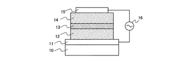
図1は、絶縁表面を有する基板10上に、第1の電極11と、第1の材料層12と、有機化合物を含む層13と、第2の材料層14と、第2の電極15とを順次積層した構造を示している。なお、第1の電極11と第2の電極15に交流電源16が接続され、有機化合物を含む層13が発光する。
FIG. 1 illustrates a
第1の電極11および第2の電極15は、両方、もしくは一方が透光性を有する導電膜を用いる。透光性を有する導電膜としては、ITO、IZO、ITSOを用いればよい。第1の電極11および第2の電極15の膜厚は、10nm〜500nmの範囲とする。第1の電極11および第2の電極15の膜厚は、10nm以下であると、電導性が著しく低下するため電極として機能せず、500nmよりも厚くしてしまうと透光性が低下する。
The
また、第1の電極11もしくは第2の電極15として金属膜を用いる場合には、Ag、Al、Taなどを用いることができる。
In the case where a metal film is used as the
また、第1の材料層12および第2の材料層14は、電流値を横軸にとり、電圧値を縦軸にとったグラフ表示においてゼロを中心としたほぼ点対称な電流−電圧特性を有する材料を用いる。具体的には、第1の材料層12および第2の材料層14は、金属酸化物(酸化モリブデン、酸化タングステン、酸化レニウムなど)と有機化合物(ホール輸送性を有する材料(例えば4,4’−ビス[N−(3−メチルフェニル)−N−フェニルアミノ]ビフェニル(略称:TPD)、4,4’−ビス[N−(1−ナフチル)−N−フェニルアミノ]ビフェニル(略称:α−NPD)、4,4’−ビス{N−[4−(N,N−ジ−m−トリルアミノ)フェニル]−N−フェニルアミノ}ビフェニル(略称:DNTPD)など))とを含む複合層とする。
Further, the
また、第1の材料層12および第2の材料層14の膜厚は、3nm〜1000nmの範囲とする。膜厚が3nm未満であると、膜として一面に形成することができず、1000nmよりも厚くなると透光性が著しく低下してしまう。
The film thicknesses of the
また、有機化合物を含む層13は、単層でも積層でもよく、一つの層の厚さは5nm〜500nmとする。図1の発光素子の構造において、単層とした場合にはもっともシンプルな積層構造となる。
The
また、有機化合物を含む層13に用いる材料は、例えば、トリス(8−キノリノラト)アルミニウム(略称:Alq3)や、トリス(4−メチル−8−キノリノラト)アルミニウム(略称:Almq3)や、α−NPDなどを用いることができる。また、有機化合物を含む層13は、ドーパント材料を含ませてもよく、例えば、N,N’−ジメチルキナクリドン(略称:DMQd)や、クマリン6や、ルブレンなどを用いることができる。
Examples of a material used for the
なお、有機化合物を含む層13は、最高被占軌道(HOMO)と最低空軌道(LUMO)の準位が、第1の材料層12及び第2の材料層14に含まれる金属酸化物のバンドギャップの範囲内にあるものを用いることが好ましい。
Note that the
また、第1の電極11および第2の電極15は、材料の仕事関数が、第1の材料層12及び第2の材料層14に含まれる金属酸化物のバンドギャップの範囲内とすることが好ましい。
The
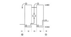
図1に示す発光素子に交流電源16から交流信号を印加し、図2および図3に示すエネルギー準位を用いて発光に至る動作機構を用いて説明する。なお、図2および図3において、図1と対応する部分には同じ符号を用いる。
Description will be made using an operation mechanism in which an AC signal is applied from the
図2において、発光素子の第1の電極11はITOとし、第2の電極15はAlとしたエネルギー準位の様子を一例として示している。
FIG. 2 shows an example of energy levels in which the
第1の電極11と第2の電極15との間に電圧を印加すると、第1の材料層12および第2の材料層14で電荷が発生する。第1の電極11に接する第1の材料層12では、発生した電荷のうち、電子が第1の電極11へ移動し、正孔は有機化合物を含む層13へ注入される。
When a voltage is applied between the
一方、第2の電極15に接する第2の材料層14では、発生した電荷のうち、電子が有機化合物を含む層13へ注入され、正孔は第2の電極15へ移動する。
On the other hand, in the
こうして、第1の材料層12から注入された正孔と、第2の材料層14から注入された電子とが再結合して有機化合物を含む層13で発光する。
In this way, holes injected from the
また、図3は、図2に示した信号とは逆極性の信号が印加されたエネルギー準位の様子を示している。逆極性の信号が印加されても、同じ素子構成であるため、同様に有機化合物を含む層13で発光する。
FIG. 3 shows the state of energy levels when a signal having a polarity opposite to that of the signal shown in FIG. 2 is applied. Even when a signal having a reverse polarity is applied, light is emitted from the
以上に示したように本発明の発光素子に交流信号を印加すると、ある極性の電圧が印加された半周期だけでなく、逆極性の電圧を印加しても発光させることができる。 As described above, when an AC signal is applied to the light-emitting element of the present invention, light emission can be performed not only by a half cycle in which a voltage having a certain polarity is applied but also by applying a voltage having a reverse polarity.
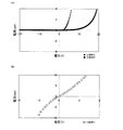
また、以下に示す実験を行い、得られた結果を図4に示す。 Moreover, the experiment shown below was conducted and the obtained result is shown in FIG.
ガラス基板上にITSO膜と、酸化モリブデンとDNTPDとルブレンとを3つ同時に任意の割合で蒸着させた複合膜と、アルミニウム膜とを積層したサンプル1と、ガラス基板上にITSO膜と、酸化モリブデンとBBPBとルブレンとを3つ同時に任意の割合で蒸着させた複合膜と、アルミニウム膜とを積層したサンプル2をそれぞれ作製した。
Sample 1 in which an ITSO film, a composite film in which three molybdenum oxides, DNTPD, and rubrene are vapor-deposited at an arbitrary ratio at the same time, and an aluminum film are laminated on a glass substrate, an ITSO film, and a molybdenum oxide film on a
そして、サンプル1とサンプル2に対して電流および電圧を印加して、電流値を横軸にとり、電圧値を縦軸にとってそれぞれグラフ表示させた。
Then, current and voltage were applied to Sample 1 and
サンプル1の一対の電極(ITSO膜とアルミニウム膜)に挟まれた材料は、図4に示すように、ゼロを中心としたほぼ点対称な電流−電圧特性を有する材料層であることが読み取れる。また、サンプル2も同様に、ゼロを中心としたほぼ点対称な電流−電圧特性を有する材料層である。
As shown in FIG. 4, it can be seen that the material sandwiched between the pair of electrodes (ITSO film and aluminum film) of Sample 1 is a material layer having current-voltage characteristics that are substantially point-symmetric with respect to zero. Similarly, the
また、比較例1として、ガラス基板上にITSO膜と、DNTPD膜と、アルミニウム膜とを積層して、電流−電圧特性を測定した結果を図14(A)に示す。また、比較例1として、ガラス基板上にITSO膜と、BBPB膜と、アルミニウム膜とを積層して、電流−電圧特性を測定した結果も図14(A)に示す。図14(A)に示すように、一対の電極に有機化合物膜を単層として挟んだ場合には、正の電圧を印加した時にしか電流は流れない。 As Comparative Example 1, FIG. 14A shows the result of measuring current-voltage characteristics by stacking an ITSO film, a DNTPD film, and an aluminum film over a glass substrate. As Comparative Example 1, FIG. 14A also shows the results of measuring current-voltage characteristics by stacking an ITSO film, a BBPB film, and an aluminum film over a glass substrate. As shown in FIG. 14A, when an organic compound film is sandwiched between a pair of electrodes as a single layer, current flows only when a positive voltage is applied.
また、比較例3として、ガラス基板上にITSO膜と、酸化モリブデン膜と、アルミニウム膜とを積層して、電流−電圧特性を測定した結果を図14(B)に示す。図14(B)に示すように、一対の電極に酸化モリブデン膜を単層として挟んだ場合には、対称な電流−電圧特性を示さない。 As Comparative Example 3, FIG. 14B shows the results of measuring current-voltage characteristics by stacking an ITSO film, a molybdenum oxide film, and an aluminum film over a glass substrate. As shown in FIG. 14B, when a molybdenum oxide film is sandwiched between a pair of electrodes as a single layer, symmetrical current-voltage characteristics are not exhibited.
以上の構成でなる本発明について、以下に示す実施例でもってさらに詳細な説明を行うこととする。 The present invention having the above-described configuration will be described in more detail with the following examples.
本実施例ではパッシブ型の表示装置の発光素子として本発明の発光素子の構造を用いた例を図5(A)〜図5(C)に示す。 In this embodiment, an example in which the structure of the light-emitting element of the present invention is used as a light-emitting element of a passive display device is shown in FIGS.
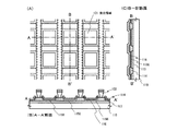
図5(A)は、封止前における画素部の上面図を示す図であり、図5(A)中の鎖線A−A’で切断した断面図が図5(B)であり、鎖線B−B’で切断した断面図が図5(C)である。 5A is a diagram illustrating a top view of the pixel portion before sealing, and a cross-sectional view taken along the chain line AA ′ in FIG. 5A is FIG. FIG. 5C is a cross-sectional view taken along −B ′.
第1の基板110上には、ストライプ状に複数の第1の電極113が等間隔で配置されている。また、第1の電極113上には、各画素に対応する開口部を有する隔壁114が設けられ、開口部を有する隔壁114は感光性または非感光性の有機材料(ポリイミド、アクリル、ポリアミド、ポリイミドアミド、レジストまたはベンゾシクロブテン)、またはSOG膜(例えば、アルキル基を含むSiOx膜))で構成されている。なお、各画素に対応する開口部が発光領域121となる。
On the
開口部を有する隔壁114上に、第1の電極113と交差する互いに平行な複数の逆テーパ状の隔壁122が設けられる。逆テーパ状の隔壁122はフォトリソグラフィ法に従い、未露光部分がパターンとしてポジ型感光性樹脂を用い、パターンの下部がより多くエッチングされるように露光量または現像時間を調節することによって形成する。
A plurality of reverse-tapered
また、平行な複数の逆テーパ状の隔壁122を形成した直後における斜視図を図6に示す。なお、図5(A)〜図5(C)と同一の部分には同一の符号を用いている。
FIG. 6 shows a perspective view immediately after forming a plurality of parallel reverse-tapered
逆テーパ状の隔壁122の高さは、有機化合物を含む膜及び導電膜の膜厚より大きく設定する。図6に示す構成を有する第1の基板に対して有機化合物を含む膜と、導電膜とを積層形成すると、図5に示すように電気的に独立した複数の領域に分離され、有機化合物を含む層115R、115G、115Bと、第2の電極116とが形成される。第2の電極116は、第1の電極113と交差する方向に伸長する互いに平行なストライプ状の電極である。なお、逆テーパ状の隔壁122上にも有機化合物を含む膜及び導電膜が形成されるが、有機化合物を含む層115R、115G、115B及び第2の電極116とは分断されている。
The height of the inversely tapered
本実施例では、第1の電極上に、金属酸化物と有機化合物とを含む第1の複合層と、有機化合物を含む層と、金属酸化物と有機化合物とを含む第2の複合層の積層115R、115G、115Bを選択的に形成し、3種類(赤色、緑色、青色)の発光が得られるフルカラー表示可能な発光装置を形成する例を示している。積層115R、115G、115Bはそれぞれ互いに平行なストライプパターンで形成されている。ここでは、積層を同じパターンとしたが、第1の複合層と第2の複合層とを各発光素子に共通な層とし、発光層となる有機化合物を含む層のみを蒸着マスクを用いて選択的に蒸着させてもよい。
In this embodiment, a first composite layer containing a metal oxide and an organic compound, a layer containing an organic compound, and a second composite layer containing a metal oxide and an organic compound are formed on the first electrode. In the example, the
金属酸化物と有機化合物とを含む第1の複合層の成膜例を示す。まず、NPBと酸化モリブデンとをそれぞれ別の抵抗加熱式の蒸発源に収納し、真空に引かれた蒸着装置内に設置された第1の電極を有する基板に対して蒸着する。蒸着時において、NPBは0.4nm/sの成膜レートで蒸着させ、酸化モリブデンはNPBに対して1/4の量(重量比)を蒸発させる。この場合、モル比では、NPB:酸化モリブデン=1:1となっている。金属酸化物と有機化合物とを含む第1の複合層の膜厚は50nmとする。 An example of forming a first composite layer containing a metal oxide and an organic compound is shown. First, NPB and molybdenum oxide are housed in separate resistance-heating evaporation sources, and are deposited on a substrate having a first electrode installed in a vacuum-deposited deposition apparatus. At the time of vapor deposition, NPB is vapor-deposited at a film formation rate of 0.4 nm / s, and molybdenum oxide evaporates an amount (weight ratio) of 1/4 with respect to NPB. In this case, the molar ratio is NPB: molybdenum oxide = 1: 1. The thickness of the first composite layer including the metal oxide and the organic compound is 50 nm.
次いで、第1の複合層上に、青色の発光素子を形成しようとする領域に青色の発光層としてCBP(4,4'−ビス(N−カルバゾリル)−ビフェニル)が添加されたPPD(4,4'−ビス(N−(9−フェナントリル)−N−フェニルアミノ)ビフェニル)を膜厚30nmで蒸着する。 Next, on the first composite layer, a PPD (4,4) in which CBP (4,4′-bis (N-carbazolyl) -biphenyl) is added as a blue light-emitting layer in a region where a blue light-emitting element is to be formed. 4′-bis (N- (9-phenanthryl) -N-phenylamino) biphenyl) is deposited with a film thickness of 30 nm.
また、赤色の発光素子を形成しようとする領域に赤色の発光層としてDCMが添加されたAlq3を膜厚40nmで成膜する。 In addition, Alq 3 to which DCM is added as a red light emitting layer is formed to a thickness of 40 nm in a region where a red light emitting element is to be formed.
また、緑色の発光素子を形成しようとする領域に緑色の発光層としてDMQDが添加されたAlq3を膜厚40nmで成膜する。 In addition, Alq 3 to which DMQD is added as a green light emitting layer is formed to a thickness of 40 nm in a region where a green light emitting element is to be formed.
そして、青色の発光層、赤色の発光層、および緑色の発光層上に金属酸化物と有機化合物とを含む第2の複合層を形成する。第2の複合層は、第1の複合層と同様にしてNPBと酸化モリブデンとを蒸着して得る。第2の複合層の膜厚も50nmとする。なお、発光色毎に第1の複合層や第2の複合層の膜厚を適宜変更して発光効率を向上させてもよい。 Then, a second composite layer including a metal oxide and an organic compound is formed over the blue light-emitting layer, the red light-emitting layer, and the green light-emitting layer. The second composite layer is obtained by evaporating NPB and molybdenum oxide in the same manner as the first composite layer. The film thickness of the second composite layer is also 50 nm. Note that the light emission efficiency may be improved by appropriately changing the film thickness of the first composite layer or the second composite layer for each emission color.
また、4種類(赤色、緑色、青色、白色)の発光が得られるフルカラー表示可能な発光装置を形成してもよい。また、4種類(赤色、緑色、青色、エメラルドグリーン)の発光が得られるフルカラー表示可能な発光装置を形成してもよい。さらに、5種類(赤色、緑色、青色、白色、エメラルドグリーン)の発光が得られるフルカラー表示可能な発光装置を形成してもよい。また、5種類(赤色、緑色、青色、エメラルドグリーン、朱黄色)の発光が得られるフルカラー表示可能な発光装置を形成してもよい。 Further, a light emitting device capable of full color display capable of obtaining four types of light emission (red, green, blue, and white) may be formed. Further, a light emitting device capable of full color display capable of obtaining four types of light emission (red, green, blue, emerald green) may be formed. Further, a light emitting device capable of full color display capable of obtaining five types of light emission (red, green, blue, white, emerald green) may be formed. Further, a light emitting device capable of full color display capable of obtaining five types of light emission (red, green, blue, emerald green, and vermilion yellow) may be formed.
また、全面に積層を形成し、単色の発光素子を設けてもよく、モノクロ表示可能な発光装置、或いはエリアカラー表示可能な発光装置としてもよい。また、白色発光が得られる発光装置として、カラーフィルタと組み合わせることによってフルカラー表示可能な発光装置としてもよい。 Alternatively, a single layer of light emitting element may be provided over the entire surface, and a light emitting device capable of monochrome display or a light emitting device capable of area color display may be used. Alternatively, a light-emitting device that can emit white light may be a light-emitting device capable of full-color display by being combined with a color filter.
また、発光素子の封止は、シール材を用いて第2の基板を貼り合わせることによって行う。必要があれば、第2の電極116を覆う保護膜を形成してもよい。なお、第2の基板としては、水分に対するバリア性の高い基板が好ましい。また、必要であれば、シール材で囲まれた領域に乾燥剤を配置してもよい。
In addition, the light-emitting element is sealed by bonding the second substrate with a sealant. If necessary, a protective film covering the
また、第1の電極113を光反射性を有する導電材料とし、第2の電極116を透光性を有する導電材料とした場合には、発光素子からの発光を第2の基板を通過させて取り出すトップエミッション型の発光装置とすることができる。第1の電極113として、炭素及びニッケルを含むアルミニウム合金(Al(C+Ni))膜を単層、或いは透明導電膜との積層の下層に用いると、通電、或いは熱処理後もITOやITSOとのコンタクト抵抗値に大きな変動がない材料であるため好ましい。
In the case where the
また、第1の電極113を透光性を有する導電材料とし、第2の電極116を光反射性を有する導電材料とした場合には、発光素子からの発光を第1の基板110を通過させて取り出すボトムエミッション型の発光装置とすることができる。
In the case where the
また、第1の電極113および第2の電極116をともに透光性を有する導電材料とした場合には、発光素子からの発光を第2の基板を通過させることと、発光素子からの発光を第1の基板を通過させることを両方行うことが可能な発光装置とすることができる。
In the case where both the
また、封止を行った後、FPCなどを実装した発光モジュールの上面図を図7に示す。 Further, FIG. 7 shows a top view of a light emitting module on which an FPC or the like is mounted after sealing.
第1の基板301と第2の基板310とが対向するようにシール材311で貼り付けられている。シール材311としては光硬化樹脂を用いれば良く、脱ガスが少なく、吸湿性の低い材料が好ましい。また、シール材311は基板間隔を一定に保つため、フィラー(棒状またはファイバー状のスペーサ)や球状のスペーサを添加したものであっても良い。なお、第2の基板310としては第1の基板401と熱膨張係数が同一の材料が好ましく、ガラス(石英ガラスを含む)もしくはプラスチックを用いることができる。
The
図7に示すように画像表示を構成する画素部は、走査線群とデータ線群が互いに直交するように交差している。 As shown in FIG. 7, the pixel portions constituting the image display intersect so that the scanning line group and the data line group are orthogonal to each other.
図5(B)における第1の電極113が図6の走査線302に相当し、第2の電極116がデータ線303に相当し、逆テーパ状の隔壁122が隔壁304に相当する。データ線302と走査線303の間には有機化合物を含む積層が挟まれており、305で示される交差部が画素1つ分となる。
The
なお、走査線303は配線端で接続配線308と電気的に接続され、接続配線308が入力端子307を介してFPC309bに接続される。また、データ線は入力端子306を介してFPC309aに接続される。
Note that the
また、必要であれば、出射面に偏光板、又は円偏光板(楕円偏光板を含む)、位相差板(λ/4板、λ/2板)、カラーフィルタなどの光学フィルムを適宜設けてもよい。また、偏光板又は円偏光板に反射防止膜を設けてもよい。例えば、表面の凹凸により反射光を拡散し、映り込みを低減できるアンチグレア処理を施すことができる。また偏光板、又は円偏光板に加熱処理を施すアンチリフレクション処理を施してもよい。その後さらに、外部衝撃から保護するためハードコート処理を施すとよい。ただし、偏光板、又は円偏光板を用いると、偏光板、又は円偏光板により光の取り出し効率が低下してしまう。また、偏光板、又は円偏光板自体のコストが高く、且つ、劣化しやすい。 Further, if necessary, an optical film such as a polarizing plate or a circular polarizing plate (including an elliptical polarizing plate), a retardation plate (λ / 4 plate, λ / 2 plate), a color filter, etc. is appropriately provided on the exit surface. Also good. Further, an antireflection film may be provided on the polarizing plate or the circularly polarizing plate. For example, anti-glare treatment that diffuses reflected light due to surface irregularities and can reduce reflection can be performed. Moreover, you may perform the anti-reflection process which heat-processes to a polarizing plate or a circularly-polarizing plate. Thereafter, in order to protect from external impact, a hard coat treatment may be performed. However, when a polarizing plate or a circularly polarizing plate is used, the light extraction efficiency decreases due to the polarizing plate or the circularly polarizing plate. In addition, the cost of the polarizing plate or the circularly polarizing plate itself is high and easily deteriorates.
こうして得られた図7に示す発光モジュールを交流駆動させる。本発明の発光素子は交流駆動させても、正の信号と負の信号の両方で発光素子を発光させることができ、さらに消費電力を増加させることなく、直流電圧を印加する直流駆動させた場合と同等の発光量を得ることができる。 The light emitting module shown in FIG. 7 thus obtained is AC driven. Even if the light emitting device of the present invention is driven by alternating current, the light emitting device can emit light with both positive and negative signals, and further when the direct current drive is applied to apply a direct current voltage without increasing the power consumption. Can be obtained.
また、本実施例は、最良の形態と自由に組み合わせることができる。 This embodiment can be freely combined with the best mode.
本実施例では、ICチップを実装する発光モジュールの作製例を以下に示す。 In this embodiment, an example of manufacturing a light-emitting module on which an IC chip is mounted is shown below.
まず、絶縁表面を有する第1の基板401上に、下層は反射性を有する金属膜、上層は透明な酸化物導電膜とした積層構造を有するデータ線(陽極)402を形成する。同時に接続配線408、409a、409b、および入力端子も形成する。
First, on a
次いで、各画素405に対応する開口部を有する隔壁を設ける。次いで、開口部を有する隔壁上に、データ線402と交差する互いに平行な複数の逆テーパ状の隔壁404を設ける。
Next, a partition wall having an opening corresponding to each
以上に示す工程を終えた段階での上面図を図8(A)に示す。 FIG. 8A shows a top view at the stage where the steps described above are completed.
次いで、金属酸化物と有機化合物とを含む第1の複合層と、有機化合物を含む膜と、金属酸化物と有機化合物とを含む第2の複合層と、透明導電膜とを順次積層形成すると、図8(B)に示すように電気的に独立した複数の領域に分離され、有機化合物を含む層と、透明導電膜からなる走査線403とが形成される。透明導電膜からなる走査線403は、データ線402と交差する方向に伸長する互いに平行なストライプ状の電極である。
Next, a first composite layer containing a metal oxide and an organic compound, a film containing an organic compound, a second composite layer containing a metal oxide and an organic compound, and a transparent conductive film are sequentially stacked. As shown in FIG. 8B, a layer containing an organic compound and a
次いで、シール材413で透光性を有する第2の基板414を貼り付ける。
次いで、画素部の周辺(外側)の領域に、画素部へ各信号を伝送する駆動回路が形成されたデータ線側IC406、走査線側IC407をCOG方式によりそれぞれ実装する。COG方式以外の実装技術としてTCPやワイヤボンディング方式を用いて実装してもよい。TCPはTABテープにICを実装したものであり、TABテープを素子形成基板上の配線に接続してICを実装する。データ線側IC406、および走査線側IC407は、シリコン基板を用いたものであってもよいし、ガラス基板、石英基板もしくはプラスチック基板上にTFTで駆動回路を形成したものであってもよい。また、片側に一つのICを設けた例を示しているが、片側に複数個に分割して設けても構わない。
Next, a
Next, the data
なお、走査線403は配線端で接続配線408と電気的に接続され、接続配線408が走査線側IC407と接続される。これは走査線側IC407を逆テーパ状の隔壁404上に設けることが困難だからである。
Note that the
以上のような構成で設けられたデータ線側IC406は接続配線409aおよび入力端子410を介してFPC411に接続される。また、走査線側IC407は接続配線409bおよび入力端子を介してFPCに接続される。
The data
さらに、ICチップ412(メモリチップ、CPUチップ、電源回路チップなど)を実装して集積化を図っている。 Further, an IC chip 412 (memory chip, CPU chip, power supply circuit chip, etc.) is mounted for integration.
また、図8(B)中、鎖線C−Dで切断した断面構造の一例を図9に示す。 FIG. 9 illustrates an example of a cross-sectional structure cut along a chain line CD in FIG.
基板510上には下地絶縁膜511が設けられ、その上には積層からなるデータ線が形成されている。下層512は反射性を有する金属膜であり、上層513は透明な酸化物導電膜である。上層513は仕事関数の高い導電膜を用いることが好ましく、インジウム錫酸化物(ITO)の他、例えば、Si元素を含むインジウム錫酸化物(ITSO)や酸化インジウムに2〜20%の酸化亜鉛(ZnO)を混合したIZO(Indium Zinc Oxide)などの透明導電材料、もしくはこれらを組み合わせた化合物を含む膜を用いることができる。中でもITSOは、ベークを行ってもITOのように結晶化せず、アモルファス状態のままである。従って、ITSOは、ITOよりも平坦性が高く、有機化合物を含む積層が薄くとも陰極とのショートが生じにくく、発光素子の陽極として適している。
A
また、下層512は、Ag、Al、またはAl(C+Ni)合金膜を用いる。中でもAl(C+Ni)膜(炭素及びニッケル(1〜20wt%)を含むアルミニウム合金膜)は、通電、或いは熱処理後もITOやITSOとのコンタクト抵抗値に大きな変動がない材料であり、好ましい。
The
隔壁514は、隣り合うデータ線同士を絶縁化するための樹脂であり、異なる着色層(封止基板側に設けられる)との境界、或いは隙間と重なる。隔壁で囲まれた領域が発光領域と対応して同一面積になっている。
The
有機化合物を含む層515はデータ線(陽極)側から順に、第1の複合層、EML(発光層)、第2の複合層、の順に積層されている。
The
第1の複合層および第2の複合層は、金属酸化物と有機化合物とを含む複合層であり、本実施例では、酸化タングステンとTPDとの複合層とする。また、EML(発光層)は、発光物質を用いて形成する。この時、発光層は、発光物質の有するエネルギーギャップよりも大きいエネルギーギャップを有する物質からなる層中に発光物質が分散して含まれるように形成してもよい。発光物質を分散させることで、濃度に起因した消光が生じることを防ぐことができる。ここで、発光物質について特に限定はなく、赤色系の発光を得たい場合は、例えば、4−ジシアノメチレン−2−イソプロピル−6−[2−(1,1,7,7−テトラメチルジュロリジン−9−イル)エテニル]−4H−ピラン(略称:DCJTI)、4−ジシアノメチレン−2−メチル−6−[2−(1,1,7,7−テトラメチルジュロリジン−9−イル)エテニル]−4H−ピラン(略称:DCJT)、4−ジシアノメチレン−2−tert−ブチル−6−[2−(1,1,7,7−テトラメチルジュロリジン−9−イル)エテニル]−4H−ピラン(略称:DCJTB)やペリフランテン、2,5−ジシアノ−1,4−ビス[2−(10−メトキシ−1,1,7,7−テトラメチルジュロリジン−9−イル)エテニル]ベンゼン等、600nmから680nmに発光スペクトルのピークを有する発光を呈する物質を発光物質として用いればよい。また、緑色系の発光を得たいときは、N,N’−ジメチルキナクリドン(略称:DMQd)、クマリン6やクマリン545T、トリス(8−キノリノラト)アルミニウム(略称:Alq3)等、500nmから550nmに発光スペクトルのピークを有する発光を呈する物質を発光物質として用いればよい。また、青色系の発光を得たいときは、9,10−ビス(2−ナフチル)−tert−ブチルアントラセン(略称:t−BuDNA)、9,9’−ビアントリル、9,10−ジフェニルアントラセン(略称:DPA)、9,10−ビス(2−ナフチル)アントラセン(略称:DNA)、ビス(2−メチル−8−キノリノラト)−4−フェニルフェノラト−ガリウム(略称:BGaq)、ビス(2−メチル−8−キノリノラト)−4−フェニルフェノラト−アルミニウム(略称:BAlq)等、420nmから500nmに発光スペクトルのピークを有する発光を呈する物質を発光物質として用いればよい。また、発光物質を分散させるために発光物質と共に用いる物質についても特に限定はなく、例えば、9,10−ジ(2−ナフチル)−2−tert−ブチルアントラセン(略称:t−BuDNA)等のアントラセン誘導体、または4,4’−ビス(N−カルバゾリル)ビフェニル(略称:CBP)等のカルバゾール誘導体の他、ビス[2−(2−ヒドロキシフェニル)ピリジナト]亜鉛(略称:Znpp2)、ビス[2−(2−ヒドロキシフェニル)ベンゾオキサゾラト]亜鉛(略称:ZnBOX)等の金属錯体等を用いることができる。 The first composite layer and the second composite layer are composite layers containing a metal oxide and an organic compound. In this embodiment, the first composite layer and the second composite layer are composite layers of tungsten oxide and TPD. The EML (light emitting layer) is formed using a light emitting substance. At this time, the light-emitting layer may be formed so that the light-emitting substance is dispersed and included in a layer made of a substance having an energy gap larger than that of the light-emitting substance. By dispersing the light emitting substance, quenching due to concentration can be prevented. Here, there is no particular limitation on the luminescent material, and when red light emission is desired, for example, 4-dicyanomethylene-2-isopropyl-6- [2- (1,1,7,7-tetramethyljulolidine) -9-yl) ethenyl] -4H-pyran (abbreviation: DCJTI), 4-dicyanomethylene-2-methyl-6- [2- (1,1,7,7-tetramethyljulolidin-9-yl) ethenyl ] -4H-pyran (abbreviation: DCJT), 4-dicyanomethylene-2-tert-butyl-6- [2- (1,1,7,7-tetramethyljulolidin-9-yl) ethenyl] -4H- Pyran (abbreviation: DCJTB), periflanthene, 2,5-dicyano-1,4-bis [2- (10-methoxy-1,1,7,7-tetramethyljulolidin-9-yl) ethenyl] benzene, etc. And a substance which exhibits emission with a peak of emission spectrum at 680nm from 00nm may be used as the luminescent material. When green light emission is desired, N, N′-dimethylquinacridone (abbreviation: DMQd), coumarin 6, coumarin 545T, tris (8-quinolinolato) aluminum (abbreviation: Alq 3 ), etc., from 500 nm to 550 nm A substance that emits light with a peak of the emission spectrum may be used as the light-emitting substance. When blue light emission is desired, 9,10-bis (2-naphthyl) -tert-butylanthracene (abbreviation: t-BuDNA), 9,9′-bianthryl, 9,10-diphenylanthracene (abbreviation) : DPA), 9,10-bis (2-naphthyl) anthracene (abbreviation: DNA), bis (2-methyl-8-quinolinolato) -4-phenylphenolato-gallium (abbreviation: BGaq), bis (2-methyl) A substance exhibiting light emission having a peak of an emission spectrum from 420 nm to 500 nm, such as -8-quinolinolato) -4-phenylphenolato-aluminum (abbreviation: BAlq), may be used as the light-emitting substance. There is no particular limitation on a substance used with the luminescent substance to disperse the luminescent substance. For example, anthracene such as 9,10-di (2-naphthyl) -2-tert-butylanthracene (abbreviation: t-BuDNA) is used. In addition to derivatives or carbazole derivatives such as 4,4′-bis (N-carbazolyl) biphenyl (abbreviation: CBP), bis [2- (2-hydroxyphenyl) pyridinato] zinc (abbreviation: Znpp 2 ), bis [2 A metal complex such as-(2-hydroxyphenyl) benzoxazolate] zinc (abbreviation: ZnBOX) can be used.
なお、EMLは、単層構造以外に、積層構造又は混合構造をとることができる。 The EML can take a laminated structure or a mixed structure in addition to a single layer structure.
走査線516(陰極)は、データ線(陽極)と交差するように形成されている。走査線516(陰極)は、ITOや、Si元素を含むインジウム錫酸化物(ITSO)や、酸化インジウムに2〜20%の酸化亜鉛(ZnO)を混合したIZOなどの透明導電膜を用いる。本実施例では、発光が封止基板520を通過する上方出射型の発光装置の例であるので走査線516は透明であることが重要である。
The scanning line 516 (cathode) is formed so as to intersect the data line (anode). As the scanning line 516 (cathode), a transparent conductive film such as ITO, indium tin oxide containing Si element (ITSO), or IZO in which indium oxide is mixed with 2 to 20% zinc oxide (ZnO) is used. In this embodiment, since it is an example of a top emission type light emitting device in which light emission passes through the sealing
また、水分や脱ガスによるダメージから発光素子を保護するため、走査線516を覆う透明な保護膜を設けてもよい。透明な保護膜としては、PCVD法による緻密な無機絶縁膜(SiN、SiNO膜など)、スパッタ法による緻密な無機絶縁膜(SiN、SiNO膜など)、炭素を主成分とする薄膜(DLC膜、CN膜、アモルファスカーボン膜)、金属酸化物膜(WO2、CaF2、Al2O3など)などを用いることが好ましい。透明とは、可視光の透過率が80〜100%であることを指す。
In addition, a transparent protective film that covers the
また、発光素子を含む画素部は、シール材519及び封止基板520で封止され、囲まれた空間を密閉なものとしている。
In addition, the pixel portion including the light-emitting element is sealed with a
シール材519としては、紫外線硬化樹脂、熱硬化樹脂、シリコーン樹脂、エポキシ樹脂、アクリル樹脂、ポリイミド樹脂、フェノール樹脂、PVC(ポリビニルクロライド)、PVB(ポリビニルブチラル)またはEVA(エチレンビニルアセテート)を用いることが可能である。また、シール材はフィラー(棒状またはファイバー状のスペーサ)や球状のスペーサを添加したものであっても良い。
As the
また、封止基板520としてガラス基板またはプラスチック基板を用いる。プラスチック基板としては、ポリイミド、ポリアミド、アクリル樹脂、エポキシ樹脂、PES(ポリエチレンサルファイル)、PC(ポリカーボネート)、PET(ポリエチレンテレフタレート)もしくはPEN(ポリエチレンナフタレート)を板状もしくはフィルム状にして用いることができる。
Further, a glass substrate or a plastic substrate is used as the sealing
なお、密閉空間518には乾燥した不活性ガスが充填されている。シール材519で囲まれた内側の密閉空間518は乾燥剤517によって微量な水分が除去され、十分乾燥されている。また、乾燥剤517としては、酸化カルシウムや酸化バリウムなどのようなアルカリ土類金属の酸化物のような化学吸着によって水分を吸収する物質を用いることが可能である。なお、他の乾燥剤として、ゼオライトやシリカゲル等の物理吸着によって水分を吸着する物質を用いてもよい。
The sealed
一方、基板510の端部には端子電極が形成され、この部分で外部回路と接続するFPC(フレキシブルプリント配線板)532を貼り合わせる。端子電極は、反射性を有する金属膜530と、透明な酸化物導電膜529と、第2の電極から延在した酸化導電膜との積層で構成しているが、特に限定されない。
On the other hand, a terminal electrode is formed at the end of the
FPC532を実装する方法は異方導電性材料もしくはメタルバンプを用いた接続方法またはワイヤボンディング方式を採用することができる。図9では異方性導電接着材531を用いて接続を行っている。
As a method for mounting the
また、画素部の周辺には、画素部へ各信号を伝送する駆動回路が形成されたICチップ523を異方導電性材料524、525により電気的に接続している。また、カラー表示に対応した画素部を形成するためには、XGAクラスでデータ線の本数が3072本であり走査線側が768本必要となる。このような数で形成されたデータ線及び走査線は画素部の端部で数ブロック毎に区分して引出線を形成し、ICの出力端子のピッチに合わせて集める。
Further, around the pixel portion, an
また、本実施例は、最良の形態または実施例1と自由に組み合わせることができる。 This embodiment can be freely combined with the best mode or embodiment 1.
本実施例では、光学フィルムを設けた例を図10(A)を用いて説明する。 In this example, an example in which an optical film is provided will be described with reference to FIG.
第1の基板610に対向して設けられた第2の基板620に光学フィルム621を設けている。本実施例では、図10(A)中に矢印で示した方向に発光する例、即ち発光素子からの発光が第2の基板620を通過してから光学フィルム621を通過する例を示しているが、特に限定されず、光学フィルムを第1の基板側に設けて、発光素子からの発光が光学フィルム621を通過してから第2の基板620を通過する構成としてもよい。
An
光学フィルム621は、偏光板、又は円偏光板(楕円偏光板を含む)、位相差板(λ/4板、λ/2板)、カラーフィルタなどの光学フィルムを指している。
The
パッシブマトリクス型発光装置の画素における発光素子は、実施例1と同様に、下層612は反射性を有する金属膜、上層613は透明な酸化物導電膜とした積層構造を有するデータ線(陽極)と、第1の材料層615aと、有機化合物を含む層615b、第2の材料層615cと、透明導電膜からなる走査線616とで構成している。また、隔壁614は樹脂材料で構成されている。
As in the first embodiment, the light emitting element in the pixel of the passive matrix light emitting device includes a data line (anode) having a laminated structure in which the
なお、第1の材料層615aおよび第2の材料層615cは、金属酸化物(酸化モリブデン、酸化タングステン、酸化レニウムなど)と有機化合物(ホール輸送性を有する材料)の複合層である。このような発光素子の積層構造とすることで交流駆動に適した発光素子としている。
Note that the
光学フィルム621として円偏光板を用いれば、下層612に外光が反射して画像の視認性が低下することを防ぐことができる。なお、円偏光板とは、具体的にはλ/4、λ/4+λ/2の位相差特性を有する位相差板、位相差フィルム、或いは位相差膜と、偏光板、偏光フィルム、或いは直線偏光膜との組み合わせからなる円偏光板(楕円偏光板を含む)を指している。ここでいう広帯域λ/4板は、可視光の範囲で一定の位相差(90度)を与えるものである。具体的には、偏光板の透過軸と、位相差フィルムの遅相軸とのなす角が45°になるように設置したものを円偏光板と呼んでいる。なお、本明細書において、円偏光板とは、円偏光フィルムをも含むものとする。
When a circularly polarizing plate is used as the
また、発光素子を白色発光素子とし、光学フィルム621としてカラーフィルタを用いれば、フルカラー表示を可能とすることもできる。
Further, when the light emitting element is a white light emitting element and a color filter is used as the
また、複数種類の光学フィルムを適宜、組み合わせてもよい。 A plurality of types of optical films may be appropriately combined.
また、本実施例は、最良の形態、実施例1、または実施例2と自由に組み合わせることができる。
In addition, this embodiment can be freely combined with the best mode, embodiment 1, or
本実施例では、ボトムエミッション型発光装置とする例を図10(B)を用いて説明する。 In this embodiment, an example of a bottom emission light-emitting device will be described with reference to FIG.
本実施例における発光素子は、透明な酸化物導電膜からなるデータ線(陽極)713と、第1の材料層715aと、有機化合物を含む層715b、第2の材料層715cと、反射性を有する導電膜からなる走査線716とで構成している。また、隔壁714は実施例3と同様に樹脂材料で構成されている。
The light-emitting element in this example has a data line (anode) 713 formed of a transparent oxide conductive film, a
なお、第1の材料層715aおよび第2の材料層715cは、金属酸化物(酸化モリブデン、酸化タングステン、酸化レニウムなど)と有機化合物(ホール輸送性を有する材料)の複合層である。このような発光素子の積層構造とすることで交流駆動に適した発光素子としている。
Note that the
発光素子からの発光は図6(B)中の矢印に示す方向、即ち、第1の基板710を通過する方向に取り出される。従って、第2の基板721は特に光透過性を有する必要はなく、金属板でもよい。また、発光素子の信頼性を向上させるために膜厚の厚い保護膜717を形成しても光の取り出し効率が低下しないので好ましい。
Light emitted from the light-emitting element is extracted in a direction indicated by an arrow in FIG. 6B, that is, a direction passing through the
また、本実施例は、最良の形態、実施例1、実施例2、または実施例3と自由に組み合わせることができる。例えば、本実施例と実施例3と組み合わせ、光学フィルムを設ける場合には、第1の基板710に光学フィルムを設ければよい。
This embodiment can be freely combined with the best mode, embodiment 1,
本実施例では、実施例1、実施例2、実施例3、および実施例4とは異なる発光装置とする例を図10(C)を用いて説明する。 In this example, an example in which the light-emitting device is different from those in Example 1, Example 2, Example 3, and Example 4 will be described with reference to FIG.
本実施例における発光素子は、透明な酸化物導電膜からなるデータ線(陽極)813と、第1の材料層815aと、有機化合物を含む層815b、第2の材料層815cと、透明な酸化物導電膜からなる走査線816とで構成している。また、隔壁814は実施例1と同様に樹脂材料で構成されている。
The light-emitting element in this example includes a data line (anode) 813 made of a transparent oxide conductive film, a
なお、第1の材料層815aおよび第2の材料層815cは、金属酸化物(酸化モリブデン、酸化タングステン、酸化レニウムなど)と有機化合物(ホール輸送性を有する材料)の複合層である。このような発光素子の積層構造とすることで交流駆動に適した発光素子としている。
Note that the
発光素子からの発光は図10(C)中の矢印に示す方向、即ち、第1の基板810を通過する方向と、第2の基板820を通過する方向との両方で取り出される。従って、第1の基板810および第2の基板820は、ともに光透過性を有する基板を用いる。
Light emitted from the light-emitting element is extracted in both the direction indicated by the arrow in FIG. 10C, that is, the direction passing through the
また、本実施例は、最良の形態、実施例1、実施例2、または実施例3と自由に組み合わせることができる。例えば、本実施例と実施例3と組み合わせ、光学フィルムを設ける場合には、第1の基板810および第2の基板820の両方に光学フィルムを設ければよい。
This embodiment can be freely combined with the best mode, embodiment 1,
本発明の発光装置、及び電子機器として、ビデオカメラ、デジタルカメラ、ナビゲーションシステム、音響再生装置(カーオーディオ、オーディオコンポ等)、ノート型コンピュータ、ゲーム機器、携帯情報端末(モバイルコンピュータ、携帯電話、携帯型ゲーム機又は電子書籍等)、記録媒体を備えた画像再生装置(具体的にはDigital Versatile Disc(DVD)等の記録媒体を再生し、その画像を表示しうるディスプレイを備えた装置)などが挙げられる。それら電子機器の具体例を図11、および図12に示す。 As a light emitting device and an electronic device of the present invention, a video camera, a digital camera, a navigation system, an audio playback device (car audio, audio component, etc.), a notebook computer, a game device, a portable information terminal (mobile computer, mobile phone, mobile phone) Type game machine or electronic book), an image playback device provided with a recording medium (specifically, a device provided with a display capable of playing a recording medium such as a digital versatile disc (DVD) and displaying the image). Can be mentioned. Specific examples of these electronic devices are shown in FIGS.
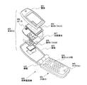
図11で示す携帯電話機は、操作スイッチ類904、マイクロフォン905などが備えられた本体(A)901と、表示パネル(A)908、表示パネル(B)909、スピーカ906などが備えられた本体(B)902とが、蝶番910で開閉可能に連結されている。表示パネル(A)908と表示パネル(B)909は、回路基板907と共に本体(B)902の筐体903の中に収納される。表示パネル(A)908及び表示パネル(B)909の画素部は筐体903に形成された開口窓から視認できように配置される。
A mobile phone shown in FIG. 11 includes a main body (A) 901 provided with operation switches 904, a
表示パネル(A)908と表示パネル(B)909は、その携帯電話機900の機能に応じて画素数などの仕様を適宜設定することができる。例えば、表示パネル(A)908を主画面とし、表示パネル(B)909を副画面として組み合わせることができる。
In the display panel (A) 908 and the display panel (B) 909, specifications such as the number of pixels can be set as appropriate in accordance with the function of the
表示パネル(A)908は、実施例1乃至5のいずれか一に示した交流駆動可能な構成を具備している。本発明により、表示パネル(A)908を交流駆動としても駆動電圧の上昇を招くことなく、携帯電話機の合計の消費電力を抑えることができる。同様に、表示パネル(B)909も交流駆動としてもよく、駆動電圧の上昇を招くことなく、携帯電話機の合計の消費電力を抑えることができる。 A display panel (A) 908 has the configuration capable of AC driving described in any one of Embodiments 1 to 5. According to the present invention, even when the display panel (A) 908 is AC driven, the total power consumption of the mobile phone can be suppressed without causing an increase in driving voltage. Similarly, the display panel (B) 909 may also be AC driven, and the total power consumption of the mobile phone can be suppressed without causing an increase in driving voltage.
本実施例に係る携帯電話機は、その機能や用途に応じてさまざまな態様に変容し得る。例えば、蝶番910の部位に撮像素子を組み込んで、カメラ付きの携帯電話機としても良い。また、操作スイッチ類904、表示パネル(A)908、表示パネル(B)909を一つの筐体内に納め、一体化させた構成としても、上記した作用効果を奏することができる。また、表示部を複数個そなえた情報表示端末に本実施例の構成を適用しても、同様な効果を得ることができる。
The mobile phone according to the present embodiment can be transformed into various modes according to the function and application. For example, a mobile phone with a camera may be obtained by incorporating an image sensor at the
図12(A)はテレビであり、筐体2001、支持台2002、表示部2003、スピーカー部2004、ビデオ入力端子2005等を含む。本発明はテレビに内蔵している表示部2003を交流駆動とし、消費電力が低減されたテレビを実現することができる。なお、パーソナルコンピュータ用、TV放送受信用、広告表示用などの全ての情報表示用のテレビが含まれる。
FIG. 12A illustrates a television, which includes a
図12(B)はデジタルカメラであり、本体2101、表示部2102、受像部2103、操作キー2104、外部接続ポート2105、シャッター2106等を含む。本発明は、デジタルカメラに内蔵されている表示部2102を交流駆動とし、消費電力が低減されたデジタルカメラとすることができる。
FIG. 12B shows a digital camera, which includes a
図12(C)はパーソナルコンピュータであり、本体2201、筐体2202、表示部2203、キーボード2204、外部接続ポート2205、ポインティングマウス2206等を含む。本発明は、パーソナルコンピュータに内蔵されている表示部2203に適用し、表示部を交流駆動とし、消費電力が低減されたパーソナルコンピュータを実現することができる。
FIG. 12C illustrates a personal computer, which includes a
図12(D)は電子書籍であり、本体2301、表示部2302、スイッチ2303、操作キー2304、赤外線ポート2305等を含む。本発明は、電子書籍に内蔵されている表示部2302を交流駆動とし、消費電力が低減された電子書籍を実現することができる。
FIG. 12D illustrates an electronic book, which includes a
図12(E)は記録媒体を備えた携帯型の画像再生装置(具体的にはDVD再生装置)であり、本体2401、筐体2402、表示部A2403、表示部B2404、記録媒体(DVD等)読み込み部2405、操作キー2406、スピーカー部2407等を含む。表示部A2403は主として画像情報を表示し、表示部B2404は主として文字情報を表示する。本発明は画像再生装置に内蔵されている表示部A2403、表示部B2404を交流駆動とし、消費電力が低減された画像再生装置を実現することができる。
FIG. 12E shows a portable image reproducing device (specifically, a DVD reproducing device) provided with a recording medium, which includes a
図12(F)は携帯型のゲーム機器であり、本体2501、表示部2503、2505、操作スイッチ2504等を含む。ゲーム機器に内蔵されている半導体集積回路(メモリやCPUなど)、および表示部2503、2505を交流駆動とし、消費電力が低減された携帯型のゲーム機器を実現することができる。 FIG. 12F illustrates a portable game machine, which includes a main body 2501, display portions 2503 and 2505, operation switches 2504, and the like. A portable game device with reduced power consumption can be realized by alternating current driving a semiconductor integrated circuit (memory, CPU, or the like) incorporated in the game device and the display portions 2503 and 2505.
図12(G)はビデオカメラであり、本体2601、表示部2602、筐体2603、外部接続ポート2604、リモコン受信部2605、受像部2606、バッテリー2607、音声入力部2608、操作キー2609等を含む。本発明は、ビデオカメラに内蔵されている半導体集積回路(メモリやCPUなど)、および表示部2602を交流駆動とし、消費電力が低減されたビデオカメラを実現することができる。
FIG. 12G illustrates a video camera, which includes a main body 2601, a display portion 2602, a
また、本実施例は実施の形態、実施例1、実施例2、実施例3、実施例4、または実施例5と自由に組み合わせることができる。
Further, this embodiment can be freely combined with Embodiment Mode, Embodiment 1,
本発明により、交流駆動法を用いたEL素子の構造をシンプルなものとすることができ、製造プロセスも簡略化することができる。また、本発明により、駆動電圧の上昇を招くことなく、一対の電極間の厚さを厚くすることができるため、EL素子形成プロセスにおけるゴミ等に起因する素子の短絡も抑制することができ、歩留まりが向上する。 According to the present invention, the structure of an EL element using an AC driving method can be simplified, and the manufacturing process can be simplified. Further, according to the present invention, since the thickness between the pair of electrodes can be increased without causing an increase in driving voltage, it is possible to suppress a short circuit of the element due to dust in the EL element forming process, Yield is improved.
10:絶縁表面を有する基板
11:第1の電極
12:第1の材料層
13:有機化合物を含む層
14:第2の材料層
15:第2の電極
16:交流電源
10: substrate having an insulating surface 11: first electrode 12: first material layer 13: layer containing an organic compound 14: second material layer 15: second electrode 16: AC power supply
Claims (5)
発光素子は、第1の電極と、
該第1の電極上に、電流値を横軸にとり、電圧値を縦軸にとったグラフ表示においてゼロを中心とした点対称な電流−電圧特性を有する第1の材料層と、
該第1の材料層上に有機化合物を含む層と、
該有機化合物を含む層上に、前記第1の材料層と同じ電流−電圧特性を有する第2の材料層と、
該第2の材料層上に第2の電極と、を有することを特徴とする発光装置。 A light emitting device having a plurality of light emitting elements,
The light emitting element includes a first electrode;
On the first electrode, a first material layer having a point-symmetric current-voltage characteristic centered on zero in a graph display in which the current value is taken on the horizontal axis and the voltage value is taken on the vertical axis;
A layer containing an organic compound on the first material layer;
A second material layer having the same current-voltage characteristics as the first material layer on the layer containing the organic compound;
A light-emitting device comprising: a second electrode on the second material layer.
5. The electronic device according to claim 1, wherein the light-emitting device is a video camera, a digital camera, a navigation, a computer, or a portable information terminal.
Priority Applications (8)
| Application Number | Priority Date | Filing Date | Title |
|---|---|---|---|
| JP2004353427A JP2006164708A (en) | 2004-12-06 | 2004-12-06 | Electronic equipment and light-emitting device |
| US11/291,312 US7521855B2 (en) | 2004-12-06 | 2005-12-01 | Electronic appliance and light-emitting device |
| CN2009101453309A CN101577315B (en) | 2004-12-06 | 2005-12-06 | Electronic appliance and light-emitting device |
| CNB2005101272697A CN100521838C (en) | 2004-12-06 | 2005-12-06 | Electronic appliance and light-emitting device |
| US12/424,262 US7999460B2 (en) | 2004-12-06 | 2009-04-15 | Electronic appliance and light-emitting device |
| US13/209,524 US8492971B2 (en) | 2004-12-06 | 2011-08-15 | Electronic appliance and light-emitting device |
| US13/946,635 US8692454B2 (en) | 2004-12-06 | 2013-07-19 | Electronic appliance and light-emitting device |
| US14/246,456 US9257489B2 (en) | 2004-12-06 | 2014-04-07 | Electronic appliance and light-emitting device |
Applications Claiming Priority (1)
| Application Number | Priority Date | Filing Date | Title |
|---|---|---|---|
| JP2004353427A JP2006164708A (en) | 2004-12-06 | 2004-12-06 | Electronic equipment and light-emitting device |
Related Child Applications (1)
| Application Number | Title | Priority Date | Filing Date |
|---|---|---|---|
| JP2011129716A Division JP4927224B2 (en) | 2011-06-10 | 2011-06-10 | Light emitting device |
Publications (2)
| Publication Number | Publication Date |
|---|---|
| JP2006164708A true JP2006164708A (en) | 2006-06-22 |
| JP2006164708A5 JP2006164708A5 (en) | 2008-01-10 |
Family
ID=36573441
Family Applications (1)
| Application Number | Title | Priority Date | Filing Date |
|---|---|---|---|
| JP2004353427A Withdrawn JP2006164708A (en) | 2004-12-06 | 2004-12-06 | Electronic equipment and light-emitting device |
Country Status (3)
| Country | Link |
|---|---|
| US (5) | US7521855B2 (en) |
| JP (1) | JP2006164708A (en) |
| CN (2) | CN101577315B (en) |
Cited By (4)
| Publication number | Priority date | Publication date | Assignee | Title |
|---|---|---|---|---|
| JP2008078011A (en) * | 2006-09-22 | 2008-04-03 | Seiko Epson Corp | Light-emitting device and electronic equipment |
| WO2008146470A1 (en) * | 2007-05-28 | 2008-12-04 | Panasonic Corporation | Organic el device and display apparatus |
| JP2013118389A (en) * | 2006-06-28 | 2013-06-13 | Semiconductor Energy Lab Co Ltd | Semiconductor device |
| US8829493B2 (en) | 2007-04-23 | 2014-09-09 | Osram Opto Semiconductors Gmbh | Electrical organic component polymeric rhenium compounds and a method for its production |
Families Citing this family (31)
| Publication number | Priority date | Publication date | Assignee | Title |
|---|---|---|---|---|
| US8426034B2 (en) * | 2005-02-08 | 2013-04-23 | Semiconductor Energy Laboratory Co., Ltd. | Light-emitting element, light-emitting device, and electronic appliance |
| US8049208B2 (en) * | 2005-04-22 | 2011-11-01 | Semiconductor Energy Laboratory Co., Ltd. | Organic semiconductor device having composite electrode |
| EP1911079A4 (en) | 2005-07-25 | 2012-05-09 | Semiconductor Energy Lab | Light-emitting element, light-emitting device, and electronic appliance |
| JP2008145840A (en) * | 2006-12-12 | 2008-06-26 | Fujifilm Corp | Display apparatus |
| DE102007023876A1 (en) * | 2007-03-02 | 2008-09-04 | Osram Opto Semiconductors Gmbh | Electric organic component comprises substrate, former electrode, which has anode, former electrically semiconducting layer on former electrode, organic functional layer on former electrically semiconducting layer |
| JP4952318B2 (en) * | 2007-03-19 | 2012-06-13 | セイコーエプソン株式会社 | Method for manufacturing electroluminescence device |
| CN101911332B (en) * | 2007-12-28 | 2012-06-13 | 夏普株式会社 | Organic electroluminescent device |
| JP5267246B2 (en) * | 2008-03-26 | 2013-08-21 | 凸版印刷株式会社 | ORGANIC ELECTROLUMINESCENT ELEMENT, ITS MANUFACTURING METHOD, AND ORGANIC ELECTROLUMINESCENT DISPLAY |
| CN102047098B (en) * | 2008-04-03 | 2016-05-04 | Qd视光有限公司 | Comprise the luminescent device of quantum dot |
| US9525148B2 (en) | 2008-04-03 | 2016-12-20 | Qd Vision, Inc. | Device including quantum dots |
| DE102008025755A1 (en) | 2008-05-29 | 2009-12-03 | Osram Opto Semiconductors Gmbh | Organic light-emitting component and light-emitting means with such a component |
| JP5476061B2 (en) * | 2008-07-30 | 2014-04-23 | パナソニック株式会社 | Organic electroluminescence device and method for manufacturing the same |
| KR101246985B1 (en) * | 2008-09-19 | 2013-03-25 | 샤프 가부시키가이샤 | Thin-film formed substrate, organic electroluminescence display device, color filter substrate, and method of producing thin-film formed substrate |
| CN102388413A (en) * | 2009-03-23 | 2012-03-21 | 夏普株式会社 | Active element substrate and manufacturing method thereof, and display apparatus using active element substrate manufactured by this manufacturing method |
| JP2011009205A (en) * | 2009-05-29 | 2011-01-13 | Semiconductor Energy Lab Co Ltd | Light emitting element, light emitting device, and method of manufacturing the same |
| CN102449800A (en) * | 2009-05-29 | 2012-05-09 | 株式会社半导体能源研究所 | Light-emitting element, light-emitting device, lighting device, and electronic appliance |
| CN101800291B (en) * | 2009-06-19 | 2012-09-26 | 深圳大学 | Organic electroluminescence device and drive method thereof |
| JP2011139044A (en) | 2009-12-01 | 2011-07-14 | Semiconductor Energy Lab Co Ltd | Luminous element, luminous device, electronic equipment, and lighting device |
| KR101692409B1 (en) * | 2010-03-29 | 2017-01-04 | 삼성디스플레이 주식회사 | Organic light emitting display apparatus and method of manufacturing thereof |
| JP2012009420A (en) * | 2010-05-21 | 2012-01-12 | Semiconductor Energy Lab Co Ltd | Light emitting device and illumination device |
| WO2012014759A1 (en) | 2010-07-26 | 2012-02-02 | Semiconductor Energy Laboratory Co., Ltd. | Light-emitting device, lighting device, and manufacturing method of light-emitting device |
| JP5827885B2 (en) * | 2010-12-24 | 2015-12-02 | 株式会社半導体エネルギー研究所 | Light emitting device and lighting device |
| JP2012182443A (en) | 2011-02-11 | 2012-09-20 | Semiconductor Energy Lab Co Ltd | Light-emitting element and light-emitting device |
| US20140346468A1 (en) * | 2013-05-27 | 2014-11-27 | Samsung Display Co., Ltd. | Organic light emitting display device having a channel in pixel defining layer |
| US10910350B2 (en) * | 2014-05-24 | 2021-02-02 | Hiphoton Co., Ltd. | Structure of a semiconductor array |
| CN104465671B (en) * | 2014-12-26 | 2016-08-31 | 京东方科技集团股份有限公司 | A kind of display base plate and preparation method thereof, display device |
| CN105118929B (en) * | 2015-08-03 | 2018-01-02 | 京东方科技集团股份有限公司 | Electrode structure and organic light-emitting units and its manufacture method |
| CN105449125B (en) * | 2015-12-03 | 2018-11-09 | 东南大学 | A kind of si-based quantum dot display and preparation method thereof |
| CN110718638B (en) * | 2018-07-11 | 2020-12-01 | Tcl科技集团股份有限公司 | Quantum dot light-emitting diode and preparation method thereof |
| CN109686851A (en) * | 2018-12-26 | 2019-04-26 | 上海晶合光电科技有限公司 | A kind of Organic Light Emitting Diode and preparation method thereof |
| CN110767836B (en) * | 2019-04-12 | 2020-08-25 | 昆山国显光电有限公司 | Semiconductor structure, display panel, preparation method of display panel and display terminal |
Citations (2)
| Publication number | Priority date | Publication date | Assignee | Title |
|---|---|---|---|---|
| JPH10513603A (en) * | 1995-03-02 | 1998-12-22 | ジ・オハイオ・ステート・ユニバーシティ | Bipolar electroluminescence device |
| JP2006024791A (en) * | 2004-07-08 | 2006-01-26 | International Manufacturing & Engineering Services Co Ltd | Organic element, organic electroluminescent element and organic solar cell |
Family Cites Families (53)
| Publication number | Priority date | Publication date | Assignee | Title |
|---|---|---|---|---|
| US5701055A (en) | 1994-03-13 | 1997-12-23 | Pioneer Electronic Corporation | Organic electoluminescent display panel and method for manufacturing the same |
| JPH08102360A (en) * | 1994-09-29 | 1996-04-16 | Toyota Central Res & Dev Lab Inc | Orfanic/inorganic complex thin-film electroluminescent element |
| JP2824411B2 (en) | 1995-08-25 | 1998-11-11 | 株式会社豊田中央研究所 | Organic thin-film light emitting device |
| TW420964B (en) * | 1998-02-25 | 2001-02-01 | Toppan Printing Co Ltd | Organic electroluminescence display substrate, method of manufacturing it and organic electroluminescent display element |
| JPH11307259A (en) | 1998-04-23 | 1999-11-05 | Tdk Corp | Organic el element |
| JP3692844B2 (en) * | 1998-07-24 | 2005-09-07 | セイコーエプソン株式会社 | Electroluminescent device and electronic device |
| JP2000268969A (en) * | 1999-03-17 | 2000-09-29 | Tdk Corp | Organic electroluminescent element |
| JP4255041B2 (en) * | 1999-04-02 | 2009-04-15 | Tdk株式会社 | Organic EL device |
| IL145317A0 (en) * | 1999-04-28 | 2002-06-30 | Du Pont | Flexible organic electronic device with improved resistance to oxygen and moisture degradation |
| KR100432998B1 (en) * | 1999-07-09 | 2004-05-24 | 삼성에스디아이 주식회사 | plasma display panel |
| TW591584B (en) | 1999-10-21 | 2004-06-11 | Semiconductor Energy Lab | Active matrix type display device |
| JP4776769B2 (en) | 1999-11-09 | 2011-09-21 | 株式会社半導体エネルギー研究所 | Method for manufacturing light emitting device |
| WO2001060125A1 (en) * | 2000-02-07 | 2001-08-16 | Tdk Corporation | Composite substrate, thin-film light-emitting device comprising the same, and method for producing the same |
| US6515310B2 (en) | 2000-05-06 | 2003-02-04 | Semiconductor Energy Laboratory Co., Ltd. | Light-emitting device and electric apparatus |
| US6864628B2 (en) * | 2000-08-28 | 2005-03-08 | Semiconductor Energy Laboratory Co., Ltd. | Light emitting device comprising light-emitting layer having triplet compound and light-emitting layer having singlet compound |
| US6893743B2 (en) * | 2000-10-04 | 2005-05-17 | Mitsubishi Chemical Corporation | Organic electroluminescent device |
| US6614175B2 (en) * | 2001-01-26 | 2003-09-02 | Xerox Corporation | Organic light emitting devices |
| US6576351B2 (en) * | 2001-02-16 | 2003-06-10 | Universal Display Corporation | Barrier region for optoelectronic devices |
| JP4869497B2 (en) | 2001-05-30 | 2012-02-08 | 株式会社半導体エネルギー研究所 | Display device |
| US6765351B2 (en) * | 2001-12-20 | 2004-07-20 | The Trustees Of Princeton University | Organic optoelectronic device structures |
| JP4310984B2 (en) * | 2002-02-06 | 2009-08-12 | 株式会社日立製作所 | Organic light emitting display |
| JP4216008B2 (en) * | 2002-06-27 | 2009-01-28 | 株式会社半導体エネルギー研究所 | LIGHT EMITTING DEVICE AND ITS MANUFACTURING METHOD, AND VIDEO CAMERA, DIGITAL CAMERA, GOGGLE TYPE DISPLAY, CAR NAVIGATION, PERSONAL COMPUTER, DVD PLAYER, ELECTRONIC GAME EQUIPMENT, OR PORTABLE INFORMATION TERMINAL HAVING THE LIGHT EMITTING DEVICE |
| TWI272874B (en) | 2002-08-09 | 2007-02-01 | Semiconductor Energy Lab | Organic electroluminescent device |
| JP4368638B2 (en) | 2002-08-09 | 2009-11-18 | 株式会社半導体エネルギー研究所 | Organic electroluminescent device |
| US7158161B2 (en) | 2002-09-20 | 2007-01-02 | Matsushita Electric Industrial Co., Ltd. | Organic electroluminescence element and an exposure unit and image-forming apparatus both using the element |
| US6965197B2 (en) * | 2002-10-01 | 2005-11-15 | Eastman Kodak Company | Organic light-emitting device having enhanced light extraction efficiency |
| US6831407B2 (en) * | 2002-10-15 | 2004-12-14 | Eastman Kodak Company | Oled device having improved light output |
| US6869698B2 (en) * | 2002-12-04 | 2005-03-22 | Canon Kabushiki Kaisha | Organic light-emitting device using paracyclophane |
| US6919681B2 (en) * | 2003-04-30 | 2005-07-19 | Eastman Kodak Company | Color OLED display with improved power efficiency |
| JP2005023154A (en) * | 2003-06-30 | 2005-01-27 | Hirose Engineering Co Ltd | Blue light emitting polymer, manufacturing process therefor and light emitting element utilizing the same |
| JP2005026121A (en) | 2003-07-03 | 2005-01-27 | Fujitsu Ltd | Organic el element and manufacturing method of the same as well as organic el display |
| AU2003294180A1 (en) | 2003-07-09 | 2005-01-28 | Matsushita Electric Industrial Co., Ltd. | Organic electroluminescence element and an exposure unit and image-forming apparatus both using the element |
| US6905788B2 (en) * | 2003-09-12 | 2005-06-14 | Eastman Kodak Company | Stabilized OLED device |
| KR101590148B1 (en) | 2003-09-26 | 2016-01-29 | 가부시키가이샤 한도오따이 에네루기 켄큐쇼 | Light emitting device and method for manufacturing light emitting element |
| EP2276088B1 (en) | 2003-10-03 | 2018-02-14 | Semiconductor Energy Laboratory Co, Ltd. | Light emitting element, and light emitting device using the light emitting element |
| US7541734B2 (en) * | 2003-10-03 | 2009-06-02 | Semiconductor Energy Laboratory Co., Ltd. | Light emitting device having a layer with a metal oxide and a benzoxazole derivative |
| JP4476594B2 (en) | 2003-10-17 | 2010-06-09 | 淳二 城戸 | Organic electroluminescent device |
| US7170176B2 (en) * | 2003-11-04 | 2007-01-30 | Semiconductor Energy Laboratory Co., Ltd. | Semiconductor device |
| JP4243237B2 (en) | 2003-11-10 | 2009-03-25 | 淳二 城戸 | Organic element, organic EL element, organic solar cell, organic FET structure, and organic element manufacturing method |
| US8796670B2 (en) | 2003-12-26 | 2014-08-05 | Semiconductor Energy Laboratory Co., Ltd. | Light-emitting element |
| JP2006295104A (en) | 2004-07-23 | 2006-10-26 | Semiconductor Energy Lab Co Ltd | Light emitting element and light emitting device using the same |
| EP1624502B1 (en) | 2004-08-04 | 2015-11-18 | Semiconductor Energy Laboratory Co., Ltd. | Light-emitting element, display device, and electronic appliance |
| EP1820372B1 (en) | 2004-09-24 | 2016-04-27 | Semiconductor Energy Laboratory Co., Ltd. | Light emitting device |
| US7737626B2 (en) | 2004-09-30 | 2010-06-15 | Semiconductor Energy Laboratory Co., Ltd. | Light emitting element |
| CN100539241C (en) | 2004-09-30 | 2009-09-09 | 株式会社半导体能源研究所 | The display device of light-emitting component and this light-emitting component of use |
| CN100583491C (en) | 2004-10-01 | 2010-01-20 | 株式会社半导体能源研究所 | Light-emitting element and light-emitting device |
| CN100573963C (en) | 2004-11-05 | 2009-12-23 | 株式会社半导体能源研究所 | Light-emitting component and its luminescent device of use |
| US7816020B2 (en) * | 2004-11-25 | 2010-10-19 | Nippon Steel Chemical Co., Ltd. | Organic electroluminescent device |
| US7771844B2 (en) * | 2004-12-03 | 2010-08-10 | Semiconductor Energy Laboratory Co., Ltd | Organic metal complex and photoelectronic device, light-emitting element and light-emitting device using the same |
| US20070216292A1 (en) | 2004-12-06 | 2007-09-20 | Satoshi Seo | Composite Material Including organic Compound And Inorganic Compound Light-Emitting Element And Light-Emitting Device Using The Composite Compound, And Manufacturing Method Of The Light-Emitting Element |
| US7948171B2 (en) * | 2005-02-18 | 2011-05-24 | Semiconductor Energy Laboratory Co., Ltd. | Light emitting device |
| EP1876658A3 (en) * | 2006-07-04 | 2014-06-25 | Semiconductor Energy Laboratory Co., Ltd. | Light-emitting element, light-emitting device, and electronic device |
| JP5554075B2 (en) * | 2009-01-21 | 2014-07-23 | 株式会社半導体エネルギー研究所 | Organometallic complex |
-
2004
- 2004-12-06 JP JP2004353427A patent/JP2006164708A/en not_active Withdrawn
-
2005
- 2005-12-01 US US11/291,312 patent/US7521855B2/en not_active Expired - Fee Related
- 2005-12-06 CN CN2009101453309A patent/CN101577315B/en not_active Expired - Fee Related
- 2005-12-06 CN CNB2005101272697A patent/CN100521838C/en not_active Expired - Fee Related
-
2009
- 2009-04-15 US US12/424,262 patent/US7999460B2/en not_active Expired - Fee Related
-
2011
- 2011-08-15 US US13/209,524 patent/US8492971B2/en not_active Expired - Fee Related
-
2013
- 2013-07-19 US US13/946,635 patent/US8692454B2/en not_active Expired - Fee Related
-
2014
- 2014-04-07 US US14/246,456 patent/US9257489B2/en not_active Expired - Fee Related
Patent Citations (2)
| Publication number | Priority date | Publication date | Assignee | Title |
|---|---|---|---|---|
| JPH10513603A (en) * | 1995-03-02 | 1998-12-22 | ジ・オハイオ・ステート・ユニバーシティ | Bipolar electroluminescence device |
| JP2006024791A (en) * | 2004-07-08 | 2006-01-26 | International Manufacturing & Engineering Services Co Ltd | Organic element, organic electroluminescent element and organic solar cell |
Cited By (9)
| Publication number | Priority date | Publication date | Assignee | Title |
|---|---|---|---|---|
| JP2013118389A (en) * | 2006-06-28 | 2013-06-13 | Semiconductor Energy Lab Co Ltd | Semiconductor device |
| JP2008078011A (en) * | 2006-09-22 | 2008-04-03 | Seiko Epson Corp | Light-emitting device and electronic equipment |
| US8829493B2 (en) | 2007-04-23 | 2014-09-09 | Osram Opto Semiconductors Gmbh | Electrical organic component polymeric rhenium compounds and a method for its production |
| WO2008146470A1 (en) * | 2007-05-28 | 2008-12-04 | Panasonic Corporation | Organic el device and display apparatus |
| JP2009200049A (en) * | 2007-05-28 | 2009-09-03 | Panasonic Corp | Organic el device |
| KR100927296B1 (en) * | 2007-05-28 | 2009-11-18 | 파나소닉 주식회사 | Organic EL Devices and Displays |
| US7683537B2 (en) | 2007-05-28 | 2010-03-23 | Panasonic Corporation | Organic EL device and display |
| JPWO2008146470A1 (en) * | 2007-05-28 | 2010-08-19 | パナソニック株式会社 | Organic EL device and display device |
| CN101543134B (en) * | 2007-05-28 | 2012-04-18 | 松下电器产业株式会社 | Organic EL device and display apparatus |
Also Published As
| Publication number | Publication date |
|---|---|
| CN1816230A (en) | 2006-08-09 |
| US20110297926A1 (en) | 2011-12-08 |
| US9257489B2 (en) | 2016-02-09 |
| US20060119258A1 (en) | 2006-06-08 |
| US8492971B2 (en) | 2013-07-23 |
| CN101577315A (en) | 2009-11-11 |
| US7521855B2 (en) | 2009-04-21 |
| US8692454B2 (en) | 2014-04-08 |
| CN100521838C (en) | 2009-07-29 |
| CN101577315B (en) | 2012-08-01 |
| US7999460B2 (en) | 2011-08-16 |
| US20130299803A1 (en) | 2013-11-14 |
| US20090251052A1 (en) | 2009-10-08 |
| US20140217387A1 (en) | 2014-08-07 |
Similar Documents
| Publication | Publication Date | Title |
|---|---|---|
| US9257489B2 (en) | Electronic appliance and light-emitting device | |
| JP6719603B2 (en) | Light emitting device | |
| JP4531342B2 (en) | White organic light emitting device and light emitting device | |
| JP4263415B2 (en) | ORGANIC LIGHT EMITTING ELEMENT AND DISPLAY DEVICE USING THE ELEMENT | |
| US7554265B2 (en) | Display device | |
| JP5063799B2 (en) | Light emitting element and display device | |
| JP5459915B2 (en) | LIGHT EMITTING DEVICE AND ELECTRIC DEVICE | |
| WO2004068911A1 (en) | Light-emitting device | |
| US6836068B2 (en) | Organic electroluminescent device and display apparatus | |
| JP2002117985A (en) | Luminescent device | |
| JP4823566B2 (en) | Light emitting element, display device, and television receiver | |
| KR20180047421A (en) | Organic Light Emitting Diode Display Device | |
| JP2005317382A (en) | Light emitting device, electronic apparatus and television apparatus | |
| JP4927224B2 (en) | Light emitting device | |
| KR100565742B1 (en) | Organic Electroluminescence Device | |
| JP2002260865A (en) | Organic electroluminescence element | |
| KR101215287B1 (en) | The lighting device | |
| KR101359914B1 (en) | Organic light emitting device |
Legal Events
| Date | Code | Title | Description |
|---|---|---|---|
| A521 | Request for written amendment filed |
Free format text: JAPANESE INTERMEDIATE CODE: A523 Effective date: 20071116 |
|
| A621 | Written request for application examination |
Free format text: JAPANESE INTERMEDIATE CODE: A621 Effective date: 20071116 |
|
| A131 | Notification of reasons for refusal |
Free format text: JAPANESE INTERMEDIATE CODE: A131 Effective date: 20100518 |
|
| A521 | Request for written amendment filed |
Free format text: JAPANESE INTERMEDIATE CODE: A523 Effective date: 20100714 |
|
| A521 | Request for written amendment filed |
Free format text: JAPANESE INTERMEDIATE CODE: A523 Effective date: 20100716 |
|
| A02 | Decision of refusal |
Free format text: JAPANESE INTERMEDIATE CODE: A02 Effective date: 20110405 |
|
| A521 | Request for written amendment filed |
Free format text: JAPANESE INTERMEDIATE CODE: A523 Effective date: 20110610 |
|
| A761 | Written withdrawal of application |
Free format text: JAPANESE INTERMEDIATE CODE: A761 Effective date: 20110613 |