JP4776769B2 - Method for manufacturing light emitting device - Google Patents
Method for manufacturing light emitting device Download PDFInfo
- Publication number
- JP4776769B2 JP4776769B2 JP2000338454A JP2000338454A JP4776769B2 JP 4776769 B2 JP4776769 B2 JP 4776769B2 JP 2000338454 A JP2000338454 A JP 2000338454A JP 2000338454 A JP2000338454 A JP 2000338454A JP 4776769 B2 JP4776769 B2 JP 4776769B2
- Authority
- JP
- Japan
- Prior art keywords
- light
- light emitting
- emitting device
- filler
- substrate
- Prior art date
- Legal status (The legal status is an assumption and is not a legal conclusion. Google has not performed a legal analysis and makes no representation as to the accuracy of the status listed.)
- Expired - Fee Related
Links
- 238000000034 method Methods 0.000 title claims description 56
- 238000004519 manufacturing process Methods 0.000 title claims description 28
- 239000000463 material Substances 0.000 claims description 65
- 239000000945 filler Substances 0.000 claims description 52
- 239000003566 sealing material Substances 0.000 claims description 40
- 229920005989 resin Polymers 0.000 claims description 14
- 239000011347 resin Substances 0.000 claims description 14
- 125000006850 spacer group Chemical group 0.000 claims description 14
- 239000012212 insulator Substances 0.000 claims description 13
- 239000000126 substance Substances 0.000 claims description 13
- 238000005401 electroluminescence Methods 0.000 description 66
- 239000000758 substrate Substances 0.000 description 57
- 230000008569 process Effects 0.000 description 22
- 238000002347 injection Methods 0.000 description 19
- 239000007924 injection Substances 0.000 description 19
- 239000004973 liquid crystal related substance Substances 0.000 description 18
- 210000004027 cell Anatomy 0.000 description 17
- 239000011159 matrix material Substances 0.000 description 12
- QVGXLLKOCUKJST-UHFFFAOYSA-N atomic oxygen Chemical compound [O] QVGXLLKOCUKJST-UHFFFAOYSA-N 0.000 description 11
- 239000001301 oxygen Substances 0.000 description 11
- 229910052760 oxygen Inorganic materials 0.000 description 11
- 239000000565 sealant Substances 0.000 description 11
- IJGRMHOSHXDMSA-UHFFFAOYSA-N Atomic nitrogen Chemical compound N#N IJGRMHOSHXDMSA-UHFFFAOYSA-N 0.000 description 10
- 239000011368 organic material Substances 0.000 description 10
- 229910052581 Si3N4 Inorganic materials 0.000 description 9
- HQVNEWCFYHHQES-UHFFFAOYSA-N silicon nitride Chemical compound N12[Si]34N5[Si]62N3[Si]51N64 HQVNEWCFYHHQES-UHFFFAOYSA-N 0.000 description 9
- XKRFYHLGVUSROY-UHFFFAOYSA-N Argon Chemical compound [Ar] XKRFYHLGVUSROY-UHFFFAOYSA-N 0.000 description 6
- QVQLCTNNEUAWMS-UHFFFAOYSA-N barium oxide Chemical compound [Ba]=O QVQLCTNNEUAWMS-UHFFFAOYSA-N 0.000 description 6
- 238000007789 sealing Methods 0.000 description 6
- 238000010586 diagram Methods 0.000 description 5
- 229910052757 nitrogen Inorganic materials 0.000 description 5
- 210000002858 crystal cell Anatomy 0.000 description 4
- 230000006866 deterioration Effects 0.000 description 4
- 239000007789 gas Substances 0.000 description 4
- 229910052786 argon Inorganic materials 0.000 description 3
- 230000015572 biosynthetic process Effects 0.000 description 3
- 230000005284 excitation Effects 0.000 description 3
- 230000006872 improvement Effects 0.000 description 3
- 239000007788 liquid Substances 0.000 description 3
- 239000004065 semiconductor Substances 0.000 description 3
- 229920001187 thermosetting polymer Polymers 0.000 description 3
- 230000008901 benefit Effects 0.000 description 2
- 239000002274 desiccant Substances 0.000 description 2
- 238000005538 encapsulation Methods 0.000 description 2
- 239000003822 epoxy resin Substances 0.000 description 2
- 239000011152 fibreglass Substances 0.000 description 2
- 239000011521 glass Substances 0.000 description 2
- 238000010438 heat treatment Methods 0.000 description 2
- 230000005525 hole transport Effects 0.000 description 2
- 229910010272 inorganic material Inorganic materials 0.000 description 2
- 239000011147 inorganic material Substances 0.000 description 2
- 150000002500 ions Chemical class 0.000 description 2
- 230000003647 oxidation Effects 0.000 description 2
- 238000007254 oxidation reaction Methods 0.000 description 2
- 238000002161 passivation Methods 0.000 description 2
- 229920003023 plastic Polymers 0.000 description 2
- 239000004033 plastic Substances 0.000 description 2
- 229920002037 poly(vinyl butyral) polymer Polymers 0.000 description 2
- 229920000647 polyepoxide Polymers 0.000 description 2
- 229920000915 polyvinyl chloride Polymers 0.000 description 2
- 239000004800 polyvinyl chloride Substances 0.000 description 2
- 229920002620 polyvinyl fluoride Polymers 0.000 description 2
- 230000005855 radiation Effects 0.000 description 2
- 229920002050 silicone resin Polymers 0.000 description 2
- QTBSBXVTEAMEQO-UHFFFAOYSA-M Acetate Chemical compound CC([O-])=O QTBSBXVTEAMEQO-UHFFFAOYSA-M 0.000 description 1
- 239000004925 Acrylic resin Substances 0.000 description 1
- 229920000178 Acrylic resin Polymers 0.000 description 1
- 229910000838 Al alloy Inorganic materials 0.000 description 1
- 229920002799 BoPET Polymers 0.000 description 1
- OKTJSMMVPCPJKN-UHFFFAOYSA-N Carbon Chemical compound [C] OKTJSMMVPCPJKN-UHFFFAOYSA-N 0.000 description 1
- 239000005977 Ethylene Substances 0.000 description 1
- 239000005041 Mylar™ Substances 0.000 description 1
- 229920001609 Poly(3,4-ethylenedioxythiophene) Polymers 0.000 description 1
- NIXOWILDQLNWCW-UHFFFAOYSA-N acrylic acid group Chemical group C(C=C)(=O)O NIXOWILDQLNWCW-UHFFFAOYSA-N 0.000 description 1
- 230000009471 action Effects 0.000 description 1
- 230000000903 blocking effect Effects 0.000 description 1
- 229910052799 carbon Inorganic materials 0.000 description 1
- 229910010293 ceramic material Inorganic materials 0.000 description 1
- 239000011248 coating agent Substances 0.000 description 1
- 238000000576 coating method Methods 0.000 description 1
- 230000000295 complement effect Effects 0.000 description 1
- 238000005520 cutting process Methods 0.000 description 1
- 230000003247 decreasing effect Effects 0.000 description 1
- 239000012769 display material Substances 0.000 description 1
- 230000000694 effects Effects 0.000 description 1
- 238000001704 evaporation Methods 0.000 description 1
- RBTKNAXYKSUFRK-UHFFFAOYSA-N heliogen blue Chemical compound [Cu].[N-]1C2=C(C=CC=C3)C3=C1N=C([N-]1)C3=CC=CC=C3C1=NC([N-]1)=C(C=CC=C3)C3=C1N=C([N-]1)C3=CC=CC=C3C1=N2 RBTKNAXYKSUFRK-UHFFFAOYSA-N 0.000 description 1
- 239000001307 helium Substances 0.000 description 1
- 229910052734 helium Inorganic materials 0.000 description 1
- SWQJXJOGLNCZEY-UHFFFAOYSA-N helium atom Chemical compound [He] SWQJXJOGLNCZEY-UHFFFAOYSA-N 0.000 description 1
- 239000007769 metal material Substances 0.000 description 1
- 230000004048 modification Effects 0.000 description 1
- 238000012986 modification Methods 0.000 description 1
- 229910052754 neon Inorganic materials 0.000 description 1
- GKAOGPIIYCISHV-UHFFFAOYSA-N neon atom Chemical compound [Ne] GKAOGPIIYCISHV-UHFFFAOYSA-N 0.000 description 1
- 230000003287 optical effect Effects 0.000 description 1
- 239000013307 optical fiber Substances 0.000 description 1
- 239000005011 phenolic resin Substances 0.000 description 1
- 239000002985 plastic film Substances 0.000 description 1
- 229920006255 plastic film Polymers 0.000 description 1
- 229920006267 polyester film Polymers 0.000 description 1
- 229920001721 polyimide Polymers 0.000 description 1
- 239000009719 polyimide resin Substances 0.000 description 1
- 229920000642 polymer Polymers 0.000 description 1
- 229920000123 polythiophene Polymers 0.000 description 1
- 239000010453 quartz Substances 0.000 description 1
- 238000005215 recombination Methods 0.000 description 1
- 230000006798 recombination Effects 0.000 description 1
- 230000009467 reduction Effects 0.000 description 1
- 238000007650 screen-printing Methods 0.000 description 1
- VYPSYNLAJGMNEJ-UHFFFAOYSA-N silicon dioxide Inorganic materials O=[Si]=O VYPSYNLAJGMNEJ-UHFFFAOYSA-N 0.000 description 1
- 238000009751 slip forming Methods 0.000 description 1
- 239000002904 solvent Substances 0.000 description 1
- 239000012780 transparent material Substances 0.000 description 1
- 238000007740 vapor deposition Methods 0.000 description 1
- 229920002554 vinyl polymer Polymers 0.000 description 1
Images


Classifications
-
- H—ELECTRICITY
- H10—SEMICONDUCTOR DEVICES; ELECTRIC SOLID-STATE DEVICES NOT OTHERWISE PROVIDED FOR
- H10K—ORGANIC ELECTRIC SOLID-STATE DEVICES
- H10K71/00—Manufacture or treatment specially adapted for the organic devices covered by this subclass
-
- H—ELECTRICITY
- H10—SEMICONDUCTOR DEVICES; ELECTRIC SOLID-STATE DEVICES NOT OTHERWISE PROVIDED FOR
- H10K—ORGANIC ELECTRIC SOLID-STATE DEVICES
- H10K50/00—Organic light-emitting devices
- H10K50/80—Constructional details
- H10K50/84—Passivation; Containers; Encapsulations
- H10K50/842—Containers
- H10K50/8428—Vertical spacers, e.g. arranged between the sealing arrangement and the OLED
-
- H—ELECTRICITY
- H01—ELECTRIC ELEMENTS
- H01L—SEMICONDUCTOR DEVICES NOT COVERED BY CLASS H10
- H01L31/00—Semiconductor devices sensitive to infrared radiation, light, electromagnetic radiation of shorter wavelength or corpuscular radiation and specially adapted either for the conversion of the energy of such radiation into electrical energy or for the control of electrical energy by such radiation; Processes or apparatus specially adapted for the manufacture or treatment thereof or of parts thereof; Details thereof
- H01L31/12—Semiconductor devices sensitive to infrared radiation, light, electromagnetic radiation of shorter wavelength or corpuscular radiation and specially adapted either for the conversion of the energy of such radiation into electrical energy or for the control of electrical energy by such radiation; Processes or apparatus specially adapted for the manufacture or treatment thereof or of parts thereof; Details thereof structurally associated with, e.g. formed in or on a common substrate with, one or more electric light sources, e.g. electroluminescent light sources, and electrically or optically coupled thereto
-
- H—ELECTRICITY
- H05—ELECTRIC TECHNIQUES NOT OTHERWISE PROVIDED FOR
- H05B—ELECTRIC HEATING; ELECTRIC LIGHT SOURCES NOT OTHERWISE PROVIDED FOR; CIRCUIT ARRANGEMENTS FOR ELECTRIC LIGHT SOURCES, IN GENERAL
- H05B33/00—Electroluminescent light sources
- H05B33/02—Details
- H05B33/04—Sealing arrangements, e.g. against humidity
-
- H—ELECTRICITY
- H10—SEMICONDUCTOR DEVICES; ELECTRIC SOLID-STATE DEVICES NOT OTHERWISE PROVIDED FOR
- H10K—ORGANIC ELECTRIC SOLID-STATE DEVICES
- H10K50/00—Organic light-emitting devices
- H10K50/80—Constructional details
- H10K50/84—Passivation; Containers; Encapsulations
- H10K50/842—Containers
- H10K50/8426—Peripheral sealing arrangements, e.g. adhesives, sealants
-
- H—ELECTRICITY
- H10—SEMICONDUCTOR DEVICES; ELECTRIC SOLID-STATE DEVICES NOT OTHERWISE PROVIDED FOR
- H10K—ORGANIC ELECTRIC SOLID-STATE DEVICES
- H10K50/00—Organic light-emitting devices
- H10K50/80—Constructional details
- H10K50/84—Passivation; Containers; Encapsulations
- H10K50/846—Passivation; Containers; Encapsulations comprising getter material or desiccants
-
- H—ELECTRICITY
- H10—SEMICONDUCTOR DEVICES; ELECTRIC SOLID-STATE DEVICES NOT OTHERWISE PROVIDED FOR
- H10K—ORGANIC ELECTRIC SOLID-STATE DEVICES
- H10K71/00—Manufacture or treatment specially adapted for the organic devices covered by this subclass
- H10K71/851—Division of substrate
Description
【0001】
【発明の属する技術分野】
本発明は、電極間に発光性材料を挟んだ素子(以下、発光素子という)を有する装置(以下、発光装置という)及びその作製方法に関する。特に、EL(Electro Luminescence)が得られる発光性材料(以下、EL材料という)を用いた発光装置に関する。
【0002】
なお、本発明に用いることのできるEL材料は、一重項励起もしくは三重項励起または両者の励起を経由して発光(燐光および/または蛍光)するすべての発光性材料を含む。
【0003】
【従来の技術】
近年、発光性材料のEL現象を利用した発光素子(以下、EL素子という)を用いた発光装置(EL表示装置)の開発が進んでいる。EL表示装置は発光素子自体に発光能力があるため、液晶ディスプレイのようなバックライトが不要である。さらに視野角が広いため、屋外での用途に適している。
【0004】
EL素子に用いる発光性材料は無機材料と有機材料とがあるが、近年では駆動電圧の低い有機材料が注目されている。ところがEL素子に有機材料を用いる際の問題点として劣化の速さが挙げられている。有機材料が酸化することでキャリアの再結合の効率が極端に悪化し、EL現象が得られなくなるのである。
【0005】
EL素子に用いる有機材料の劣化を防ぐために様々な工夫が施されている。一般的には、EL素子の上にセラミックス材や金属材をかぶせ、EL素子を密封空間に閉じこめて外気から遮断する方式が知られている。東北パイオニア(株)の生産するELディスプレイには同方式が採用されている。同社ではその密封空間に乾燥剤を設けている。
【0006】
また、他の手段として、特開平9−35868号公報、特開平11−54285号公報に記載された技術が知られている。
【0007】
【発明が解決しようとする課題】
本発明は、発光素子を外気から保護するための封入(封止)方法のスループット及び歩留まりを向上させることを課題とし、発光素子を用いた発光装置の製造コストを低減することを課題とするものである。
【0008】
【課題を解決するための手段】
本発明では大型基板から複数の発光装置を形成する多面取り工程を用いることで発光素子を用いた発光装置の製造コストの低減を図る。特に、本発明の最も大きな特徴は、発光素子の封入工程を、既存の液晶ラインを転用しうる工程とし、設備投資も含めて大幅な製造コストの低減を図る点にある。
【0009】
本発明では、発光素子の封入工程を、液晶セルを形成する工程に近い工程とすることで、既存のセル組み工程に用いられる装置を僅かな改造で転用できる点に利点がある。また、液晶セルを形成する工程は既に量産化の十分な実績があり、これを転用することで大幅な歩留まりの向上が図れる。
【0010】
具体的には、発光素子の形成された絶縁体(例えば基板)の上にシール材を形成し、シール材を用いてカバー材を接着することにより、絶縁体、カバー材およびシール材で囲まれた部分を密封可能な空間(以下、セルという)とし、そのセルを樹脂または液体で充填する。本明細書中ではこの目的で用いられる樹脂または液体を充填材と呼び、その充填に真空注入法を用いる点に特徴がある。樹脂は液体状のものをセルに注入してから固化させれば良い。
【0011】
なお、本明細書中におけるEL素子を用いた発光装置には、文字情報もしくは画像情報を表示する発光装置(以下、EL表示装置という)または光源として用いる発光装置(以下、EL発光装置という)を含む。
【0012】
【発明の実施の形態】
本発明を用いて複数のアクティブマトリクス型EL表示装置を大型基板上に作製する場合について説明する。説明には図1〜図3に示した上面図を用いる。なお、各上面図には各々の上面図をA−A’及びB−B’で切った断面図も併記する。
【0013】
まず、図1(A)に示すように、表面に複数の画素部(画像表示を行うための領域)11の形成された絶縁体(ここでは基板)12上に第1のシール材13を形成する。本実施形態では1枚の基板から四つの発光装置を形成する例を示すため、第1のシール材13は四カ所に設けられている。但し、第1のシール材13を設ける数は、1枚の基板からいくつのEL表示装置を形成するかによって変更すれば良い。
【0014】
第1のシール材13は液晶ラインで用いられる公知のディスペンサー方式やスクリーン印刷方式を用いて形成すれば良い。その際、図1(A)に示すように開口部14を形成して後に充填材を注入する入り口を確保しておく。また、第1のシール材13としては紫外線硬化樹脂、熱硬化樹脂、シリコーン樹脂、エポキシ樹脂、アクリル樹脂、ポリイミド樹脂、フェノール樹脂、PVC(ポリビニルクロライド)、PVB(ポリビニルブチラル)またはEVA(エチレンビニルアセテート)を用いることが可能である。また、第1のシール材13はフィラー(棒状またはファイバー状のスペーサ)を添加したものであっても良い。
【0015】
次に、基板12全体に球状のスペーサ15を撒布する。スペーサ15は公知のものを用いることができる。また、スペーサ15の撒布は公知の湿式または乾式で行えば良く、第1のシール材13を形成する前でも後でも良い。いずれにしてもフィラー(図示せず)もしくはスペーサ15によって基板12とその上に配置するカバー材との距離を確保する。
【0016】
なお、このスペーサ15に吸湿性をもたせることは画素部11に形成されたEL素子の劣化を抑制する上で効果的である。酸化バリウムに代表される吸湿性物質からなるスペーサを用いても良い。また、スペーサ15の材料はEL素子から発した光を透過する材料であることが望ましい。
【0017】
本実施形態の場合、第1のシール材13で囲まれた領域16内にはEL素子及びそのEL素子に電気的に接続されたTFTを含む画素部が含まれる。また、画素部と共にその画素部に電気信号を伝える駆動回路も含まれても良い。勿論、画素部のみ第1のシール材13の内側に設けて駆動回路は第1のシール材13の外側に設ける構造としても良い。
【0018】
次に、図1(B)に示すように、第1のシール材13を用いて基板12にカバー材17を接着する。本明細書中では基板12、第1のシール材13及びカバー材17が一体となった基板をセル形成基板と呼ぶ。このカバー材17を接着する工程には公知の液晶セルの形成工程と同様の工程を用いれば良い。具体的には、カバー材17を基板12に合わせて貼り合わせた後、加圧し、紫外線の照射または加熱により第1のシール材13を硬化させる。
【0019】
カバー材17は基板12と同じ面積の基板(またはフィルム)を用いれば良い。基板(またはフィルム)としては、ガラス板、石英板、プラスチック板、プラスチックフィルム、FRP(Fiberglass-Reinforced Plastics)板、PVF(ポリビニルフロライド)フィルム、マイラーフィルム、ポリエステルフィルムまたはアクリルフィルムを用いることができる。
【0020】
また、EL素子から発した光の放射方向によっては透明な物質を用いる必要がある。基板12としてフィルムを用いる場合は、紫外線硬化樹脂を第1のシール材13として用いることが望ましい。
【0021】
カバー材17を貼り合わせたら、基板12及びカバー材17を分断する。基板12及びカバー材17を分断する際、公知の分断用装置を用いることが可能である。代表的には、スクライバー、ダイサーまたはレーザーを用いることが可能である。なお、スクライバーとは、基板に細い溝(スクライブ溝)を形成した後でスクライブ溝に衝撃を与え、スクライブ溝に沿った亀裂を発生させて基板を分断する装置である。また、ダイサーとは、硬質カッター(ダイシングソーともいう)を高速回転させて基板に当てて分断する装置である。
【0022】
本実施形態では分断用装置としてスクライバーを用いた例を示す。基板12及びカバー材17にスクライブ溝を形成する順序としては、まず矢印(a)の方向にスクライブ溝18aを形成し、次に、矢印(b)の方向にスクライブ溝18bを形成する。このとき、開口部14付近を通るスクライブ溝は第1のシール材13を切断するように形成する。こうすることでセルの端面に開口部14が現れるため、後の充填材の注入工程が容易となる。
【0023】
こうしてスクライブ溝18a、18bを形成したら、シリコーン樹脂等の弾性のあるバーでスクライブ溝に衝撃を与え、亀裂を発生させて基板12及びカバー材17を分断する。
【0024】
図2(A)は1回目の分断後の様子であり、各々二つのセルを含む二つのセル形成基板19、20が形成される。次に、各セル内に真空注入法により充填材21を注入する。真空注入法は液晶注入の技術として良く知られている。具体的には、まずセル形成基板19、20を真空室におき、真空中にて開口部14を充填材21に接触させる。次いで真空室にガスを流して内圧を高め、それにより開口部14からセル内へと充填材21が注入される。
【0025】
なお、本実施形態の場合、真空注入法を用いて充填材を注入するため充填材の粘度が低くないと注入にかかる時間が著しくかかってしまう。その場合は充填材を加熱して粘度を低めてから注入することが有効である。
【0026】
また、充填材21としては吸湿性の低い樹脂を用いることが好ましいが、第1のシール材13に用いることのできる材料と同一のものでも良い。なお、EL素子から発した光の放射方向によっては透明な物質を用いる必要がある。
【0027】
また、充填材21として液晶程度に粘度の低いものを用いることが好ましい。即ち充填材21の粘度は5〜100cp(好ましくは10〜30cp)が望ましい。このような粘度の充填材を選択しても良いし、溶媒等で希釈して所望の粘度としても良い。また、充填材に予め乾燥剤として吸湿性を有する物質(吸湿性物質という)を添加しておくと、さらにEL素子の劣化を防ぐことができる。
【0028】
また、粘度の高い材料を充填材として用いる場合、充填材を加熱して注入することは有効である。1×10⁴cp程度の粘度であっても、70〜100℃で加熱すれば真空注入法に用いることができる。
【0029】
こうして図2(A)に示すように充填材21が充填される。なお、本実施形態では複数のセルに対して一度に充填材21を充填する方式を示したが、このような方式は対角0.5〜1インチ程度の小さなEL表示装置の作製時に好適である。一方、対角5〜30インチ程度の大きめのEL表示装置を作製する際は、一つのセル毎に分断してから充填材21を充填すれば良い。
【0030】
以上のようにして充填材21を充填した後、充填材21を硬化させて基板12とカバー材17との密着性をさらに高める。充填材21が紫外線硬化樹脂であれば紫外線を照射し、熱硬化性樹脂であれば加熱する。但し、熱硬化性樹脂を用いる場合は、有機EL材料の耐熱性に留意する必要がある。
【0031】
次に、再び基板12及びカバー材17にスクライブ溝を形成する。順序としては、まず矢印(a)の方向にスクライブ溝22aを形成し、次に、矢印(b)の方向にスクライブ溝22bを形成する。このとき、分断後に基板12に比べてカバー材17の面積が小さくなるようにスクライブ溝を形成しておく。
【0032】
こうしてスクライブ溝22a、22bを形成したら、前述のようにスクライブ溝に衝撃を与え、セル形成基板23〜26に分断する。図3(A)は2回目の分断後の様子である。さらに、各セル形成基板23〜26には接続端子としてFPC(フレキシブルプリントサーキット)27を取り付ける。FPC27は画素部に送られる電気信号を外部機器から入力するための端子である。勿論、画素部で表示した画像を外部機器へ出力する端子として用いることもできる。
【0033】
最後に、図3(B)に示すように、セル形成基板23〜26の基板端面(第1のシール材13及び/又は充填材21の露呈部)及び接続端子であるFPC27の一部に接して第2のシール材28を形成する。第2のシール材28としては第1のシール材13に用いることのできる材料と同一のものを用いることができる。
【0034】
以上のプロセスにより図3(B)に示すようなEL表示装置が完成する。以上のように、本発明を実施すると液晶のセル組み工程と同様の装置を用いた製造ラインによって1枚の基板から複数のEL表示装置を作製することができる。例えば、620mm×720mmの基板に対応した液晶製造ラインに多少の改良を加える程度で、1枚の基板から対角13〜14インチのEL表示装置を6個作製することが可能である。従って、大幅なスループットの向上と製造コストの削減が達成できる。
【0035】
【実施例】
〔実施例1〕
本実施例では、本発明を用いて作製したアクティブマトリクス型EL表示装置について図4(A)、(B)を用いて説明する。図4(A)は、EL素子の形成されたアクティブマトリクス基板において、EL素子の封入まで行った状態を示す上面図である。点線で示された401はソース側駆動回路、402はゲート側駆動回路、403は画素部である。また、404はカバー材、405は第1のシール材、406は第2のシール材であり、第1のシール材405で囲まれた内側のカバー材とアクティブマトリクス基板との間には充填材407(図4(B))が設けられる。
【0036】
なお、408はソース側駆動回路401、ゲート側駆動回路402及び画素部403に入力される信号を伝達するための接続配線であり、外部機器との接続端子となるFPC(フレキシブルプリントサーキット)409からビデオ信号やクロック信号を受け取る。
【0037】
ここで、図4(A)をA−A’で切断した断面に相当する断面図を図4(B)に示す。なお、図4(A)、(B)では同一の部位に同一の符号を用いている。
【0038】
図4(B)に示すように、基板300上には画素部403、ソース側駆動回路401が形成されており、画素部403はEL素子に流れる電流を制御するためのTFT(以下、電流制御用TFTという)301とそのドレインに電気的に接続された画素電極302を含む複数の画素により形成される。また、ソース側駆動回路401はnチャネル型TFT303とpチャネル型TFT304とを相補的に組み合わせたCMOS回路を用いて形成される。
【0039】
画素電極302は遮光性を有する導電膜で形成され、EL素子の陰極として機能する。また、画素電極302の両端には絶縁膜305が形成され、さらに発光層306、正孔注入層307が形成される。また、その上にはEL素子の陽極308が透明導電膜でもって形成される。
【0040】
発光層306や正孔注入層307の成膜方法は公知の如何なる手段を用いても良いし、材料として有機材料または無機材料を用いることができる。また、発光層や正孔注入層だけでなく電子注入層、電子輸送層、正孔輸送層などを組み合わせた積層構造としても良い。
【0041】
また、本実施例の場合、陽極308は全画素に共通の配線としても機能し、接続配線408を経由してFPC409に電気的に接続されている。
【0042】
次に、本発明により第1のシール材405をディスペンサー等で形成し、スペーサ(図示せず)を撒布してカバー材404を貼り合わせる。そして、アクティブマトリクス基板、カバー材404及び第1のシール材405で囲まれた領域内に充填材407を真空注入法により充填する。
【0043】
また、本実施例では充填材407に予め吸湿性物質として酸化バリウムを添加しておく。なお、本実施例では吸湿性物質を充填材に添加して用いるが、塊状に分散させて充填材中に封入することもできる。また、図示されていないがスペーサの材料として吸湿性物質を用いることも可能である。
【0044】
次に、充填材407を紫外線照射または加熱により硬化させた後、第1のシール材405に形成された開口部(図示せず)を塞ぐ。さらに、第1のシール材405の露呈部、充填材407の露呈部及びFPC409の一部を覆うように第2のシール材406を設ける。第2のシール材406は第1のシール材407と同様の材料を用いれば良い。
【0045】
以上のような方式を用いてEL素子を充填材407に封入することにより、EL素子を外部から完全に遮断することができ、外部から水分や酸素等の有機材料の酸化を促す物質が侵入することを防ぐことができる。従って、信頼性の高いEL表示装置を作製することができる。
【0046】
また、本発明を用いることで既存の液晶表示装置用の製造ラインを転用させることができるため、設備投資の費用が大幅に削減可能であり、歩留まりの高いプロセスで1枚の基板から複数の発光装置を生産することができるため、大幅に製造コストを低減しうる。
【0047】
〔実施例2〕
本実施例では、本発明を用いて作製したパッシブマトリクス型EL表示装置について図5を用いて説明する。図5において、501はプラスチック基板、502はアルミニウム合金からなる陰極である。本実施例では、陰極502を蒸着法により形成する。なお、図5では図示されていないが、複数本の陰極が紙面に平行な方向へストライプ状に配列されている。
【0048】
また、ストライプ状に配列された陰極502と直交するように絶縁膜503が形成される。また、この絶縁膜503は陰極502の各々を絶縁分離するために陰極502の隙間にも設けられる。そのため、絶縁膜503を上面から見るとマトリクス状にパターニングされている。
【0049】
さらに、絶縁膜503の上に樹脂からなるバンク504が形成される。バンク504は陰極502に直交するように、紙面に垂直な方向に形成されている。また、形状は逆三角形状(逆テーパー形状)に加工される。
【0050】
次に、発光層505及び透明導電膜でなる陽極506が連続的に形成される。
発光層504が水分や酸素に弱いため、真空中または不活性雰囲気中で両者を連続的に成膜することが望ましい。発光層505は公知の如何なる材料であっても良いが、成膜の簡便性からポリマー系有機材料が好ましい。また、陽極506は蒸着法で設けることが好ましい。発光層505及び陽極506どちらもはバンク504によって形成された溝に沿って形成され、紙面に垂直な方向にストライプ状に配列される。
【0051】
なお、図示しないが、発光層505と陽極506との間にバッファ層として正孔輸送層や正孔注入層を設けることは有効である。正孔注入層としては銅フタロシアニン、ポリチオフェン、PEDOT等を用いることができる。
【0052】
以上のようにして基板501上にEL素子を形成する。なお、本実施例では下側の電極が遮光性の陰極となっているため、発光層505で発生した光は紙面において上面側(基板501とは反対側)に放射される。しかしながら、EL素子の構造を反対にし、下側の電極を透明導電膜からなる陽極とすることもできる。その場合、発光層505で発生した光は紙面において下面側(基板501側)に放射されることになる。
【0053】
また、507はICチップでありバンプ方式で基板501上に設けられている。ICチップ507は陰極502及び陽極506に電気信号を伝えるための駆動回路として設けられ、図示されないFPC(フレキシブルプリントサーキット)によって外部機器からの信号を処理する。
【0054】
その後は本発明によりEL素子の封入を行う。本実施例では、第1のシール材508として紫外線硬化樹脂を用い、カバー材509としてガラス基板を貼り付け、真空注入法により充填材510を充填する。充填材510の中には吸湿性物質511として酸化バリウムを添加する。なお、本実施例では充填材510としてエポキシ樹脂を用いる。また、発光層505から発した光が下面側に放射される場合はカバー材509が透明である必要はない。
【0055】
こうして充填材510の注入を終えたら、第1のシール材508に設けられた開口部(図示せず)を塞ぎ、第2のシール材512により第1のシール材508の露呈部及びICチップ507を覆う。このとき、図示されないがFPCの一部を覆うように設けられていても良い。
【0056】
以上のような方式を用いてEL素子を充填材510に封入することにより、EL素子を外部から完全に遮断することができ、外部から水分や酸素等の有機材料の酸化を促す物質が侵入することを防ぐことができる。従って、信頼性の高いEL表示装置を作製することができる。
【0057】
また、本発明を用いることで既存の液晶表示装置用の製造ラインを転用させることができるため、設備投資の費用が大幅に削減可能であり、歩留まりの高いプロセスで1枚の基板から複数の発光装置を生産することができるため、大幅に製造コストを低減しうる。
【0058】
〔実施例3〕
本実施例では、図1〜3で説明した方法とは異なる方法で充填材を形成する場合の例について説明する。説明には図6を用いる。
【0059】
図6(A)において、601は基板、602は画素部、603は第1のシール材である。なお、図示していないがスペーサを撒布しても良い。第1のシール材603としては、実施形態で説明した第1のシール材13と同様のものを用いることができる。但し、本実施例では図1と異なり第1のシール材603に開口部を設けない。即ち、この時点で完全に閉空間を作るように(完全に囲まれた領域を作るように)第1のシール材603を形成する。
【0060】
そして、第1のシール材603で囲まれた領域内において画素部602の上に充填材604を滴下する。勿論、充填材604に予め吸湿性物質(図示せず)を添加しておいても良い。吸湿性物質としては実施形態で説明したものと同様のものを用いることができる。この滴下工程は第1のシール材603の形成に用いるディスペンサー等の塗布成膜装置を用いれば良い。
【0061】
また、充填材604を滴下する工程は、窒素またはアルゴン等の不活性雰囲気にされたグローブボックス中で行うことが好ましい。このとき不活性雰囲気中の酸素濃度は極力低くし、好ましくは1ppm以下(さらに好ましくは0.1ppm)以下とすると良い。
【0062】
次に、図6(B)に示すように、カバー材605を第1のシール材603により接着する。その際、図6(A)のように滴下された充填材604はカバー材605によって押しつぶされ、基板601、第1のシール材603及びカバー材605で囲まれた閉空間の中に充填される。なお、このようにして形成される閉空間の容積を予め計算して、充填材604の最適な滴下量を計算しておく必要がある。
【0063】
実施形態で説明したように、充填材を真空注入法により注入する場合には充填材の粘度が低くないとスループットの低下を招く恐れがある。しかしながら、本実施例の場合は滴下しておいて押しつぶすように充填するため、粘度の高い材料を用いても殆ど問題とならないという利点がある。
【0064】
以上のようにしてカバー材605を貼り合わせたら、この後は、実施形態と同様に基板601及びカバー材605をスクライバー、ダイサーまたはレーザーにより分断し、FPC及び/またはICチップを取り付けてアクティブマトリクス型EL表示装置またはパッシブマトリクス型EL表示装置が完成する。
【0065】
なお、本実施例は実施例1に示したアクティブマトリクス型EL表示装置または実施例2に示したパッシブマトリクス型EL表示装置のどちらとも組み合わせて実施することが可能である。また、特に特殊な装置を加えることなく液晶表示装置用の製造ラインを転用することができるため、製造コストを大幅に低減することが可能である。
【0066】
〔実施例4〕
本実施例では、図1〜3で説明した方法とは異なる方法で充填材を形成する場合の例について説明する。説明には図7を用いる。
【0067】
図7(A)において、701は基板、702は画素部、703は第1のシール材である。なお、図示していないがスペーサを撒布しても良い。第1のシール材703としては、実施形態で説明した第1のシール材13と同様のものを用いることができる。但し、本実施例では図1と異なり第1のシール材703に二つの開口部704と705が設けられている。
【0068】
そして、図7(B)のようにカバー材706を貼り合わせ、707aで示される矢印の方向と707bで示される矢印の方向にスクライブ溝を形成して基板701及びカバー材706を分断する。
【0069】
このあと、開口部704に充填材を接触させれば毛細管現象によってセル708の内部に充填材(図示せず)が注入される。このように本実施例では充填材の注入方法として、毛細管現象を利用する点に特徴がある。
【0070】
この充填材の注入工程は窒素またはアルゴン等の不活性雰囲気にしたグローブボックス内で行うことが好ましい。このとき不活性雰囲気中の酸素濃度は極力低くし、好ましくは1ppm以下(さらに好ましくは0.1ppm)以下とすると良い。
【0071】
充填材を注入した後は、図2(B)以降と同様の工程を行うことでアクティブマトリクス型もしくはパッシブ型の発光装置または光源として用いる発光装置を作製することができる。
【0072】
〔実施例5〕
本発明はEL素子を基板面の全域に設けた発光装置に対して実施することも可能である。そのような発光装置(EL発光装置)は面状発光の光源として用いることが可能であり、液晶表示装置(液晶ディスプレイ)のバックライトとしての用途がある。
【0073】
本実施例のようなEL発光装置においてもEL素子の封入は非常に重要であり、その封入技術として本発明を用いることが望ましい。
【0074】
〔実施例6〕
実施例1〜5ではEL素子を用いた発光装置を例にして説明してきたが、本発明はEC(エレクトロクロミクス)表示装置、フィールドエミッションディスプレイ(FED)または半導体を用いた発光ダイオードを有する発光装置に用いることも可能である。
【0075】
特に、EC表示装置はEC現象を示す材料がEL素子と同様に酸素または水分に弱いため、外気から遮断して気密性を保つことが好ましい。その際、本発明を実施することで大幅に歩留まりを高め、さらに製造コストを低減することが可能となる。
【0076】
〔実施例7〕
実施形態及び実施例1〜6において、発光素子を形成した後は発光素子を酸素もしくは水分に晒さないようにすることが重要となるため、本発明の封入工程はすべて不活性雰囲気または真空で行われる。
【0077】
不活性雰囲気とは窒素または希ガス(代表的にはヘリウム、アルゴンまたはネオン)で充填された空間であり、グローブボックスと呼ばれる場合もある。本発明では、図1〜図3で説明した一連の工程をすべて不活性雰囲気または真空で行うため、製造ライン全体を不活性雰囲気とすることが望ましい。
【0078】
例えば、クリーンルーム内において、図1〜図3の一連の封入工程を行う装置が設置された場所を壁またはフィルム等で囲んで密閉空間とし、窒素または希ガスで充填した雰囲気とする。この場合、窒素または希ガスで陽圧状態としておけば酸素や水分が入り込むことはない。
【0079】
また、図1〜図3の一連の封入工程を行う装置が設置されたクリーンルームを全体的に酸素濃度が1ppm以下の不活性雰囲気とすることもできる。その場合、装置の操作はオートメーション化しておくことが必要である。
【0080】
〔実施例8〕
図4に示した発光装置においては、下地膜31に窒化珪素膜もしくは窒化酸化珪素膜を設け、スイッチング用TFT201および電流制御用TFT202を窒化珪素膜もしくは窒化酸化珪素膜を含むパッシベーション膜(図示せず)で覆った構成とすることが好ましい。
【0081】
このような構造とすると、スイッチング用TFT201および電流制御用TFT202が窒化珪素膜もしくは窒化酸化珪素膜で挟まれた構造となり、外部からの水分や可動イオンの侵入を効果的に防ぐことができる。
【0082】
また、図示しないパッシベーション膜上に設けた有機樹脂からなる平坦化膜32と画素電極302の間に窒化珪素膜もしくはDLC(ダイヤモンドライクカーボン)膜を設け、さらに陰極308の上に前述の窒化珪素膜もしくはDLC膜を設けることは好ましい。
【0083】
このような構造とすると、EL素子が窒化珪素膜もしくはDLC膜で挟まれた構造となり、外部からの水分や可動イオンの侵入を防ぐだけでなく、酸素の侵入をも効果的に防ぐことができる。EL素子中の発光層などの有機材料は酸素によって容易に酸化して劣化するため、本実施例のような構造とすることで大幅に信頼性を向上することができる。
【0084】
以上のように、TFTを保護するための対策とEL素子を保護するための対策を併用して施すことで電子装置全体の信頼性を高めることができる。
【0085】
なお、本実施例の構成は、実施例1〜実施例7のいずれの構成とも自由に組み合わせることが可能である。
【0086】
〔実施例9〕
本発明を実施して形成した発光装置は、自発光型であるため液晶表示装置に比べて明るい場所での視認性に優れ、しかも視野角が広い。従って、様々な電気器具の表示部として用いることができる。例えば、TV放送等を大画面で鑑賞するには対角20〜60インチのディスプレイとして本発明の発光装置を筐体に組み込んだディスプレイを用いるとよい。
【0087】
なお、発光装置を筐体に組み込んだディスプレイには、パソコン用ディスプレイ、TV放送受信用ディスプレイ、広告表示用ディスプレイ等の全ての情報表示用ディスプレイが含まれる。また、その他にも様々な電気器具の表示部として本発明の発光装置を用いることができる。
【0088】
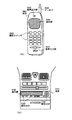
その様な本発明の電気器具としては、ビデオカメラ、デジタルカメラ、ゴーグル型ディスプレイ(ヘッドマウントディスプレイ)、ナビゲーションシステム、音響再生装置(カーオーディオ、オーディオコンポ等)、ノート型パーソナルコンピュータ、ゲーム機器、携帯情報端末(モバイルコンピュータ、携帯電話、携帯型ゲーム機または電子書籍等)、記録媒体を備えた画像再生装置(具体的にはデジタルバーサタイルディスク(DVD)等の記録媒体を再生し、その画像を表示しうるディスプレイを備えた装置)などが挙げられる。特に、斜め方向から見ることの多い携帯情報端末は視野角の広さが重要視されるため、EL表示装置を用いることが望ましい。それら電気器具の具体例を図8、図9に示す。
【0089】
図8(A)は発光装置を筐体に組み込んだディスプレイであり、筐体2001、支持台2002、表示部2003等を含む。本発明は表示部2003に用いることができる。このようなディスプレイは発光型であるためバックライトが必要なく、液晶ディスプレイよりも薄い表示部とすることができる。
【0090】
図8(B)はビデオカメラであり、本体2101、表示部2102、音声入力部2103、操作スイッチ2104、バッテリー2105、受像部2106等を含む。本発明の発光装置は表示部2102に用いることができる。
【0091】
図8(C)は頭部取り付け型のELディスプレイの一部(右片側)であり、本体2201、信号ケーブル2202、頭部固定バンド2203、表示部2204、光学系2205、発光装置2206等を含む。本発明は発光装置2206に用いることができる。
【0092】
図8(D)は記録媒体を備えた画像再生装置(具体的にはDVD再生装置)であり、本体2301、記録媒体(DVD等)2302、操作スイッチ2303、表示部(a)2304、表示部(b)2305等を含む。表示部(a)は主として画像情報を表示し、表示部(b)は主として文字情報を表示するが、本発明の発光装置はこれら表示部(a)、(b)に用いることができる。なお、記録媒体を備えた画像再生装置には家庭用ゲーム機器なども含まれる。
【0093】
図8(E)は携帯型(モバイル)コンピュータであり、本体2401、カメラ部2402、受像部2403、操作スイッチ2404、表示部2405等を含む。本発明の発光装置は表示部2405に用いることができる。
【0094】
図8(F)はパーソナルコンピュータであり、本体2501、筐体2502、表示部2503、キーボード2504等を含む。本発明の発光装置は表示部2503に用いることができる。
【0095】
なお、将来的に発光輝度がさらに高くなれば、出力した画像情報を含む光をレンズや光ファイバー等で拡大投影してフロント型若しくはリア型のプロジェクターに用いることも可能となる。
【0096】
また、発光装置は発光している部分が電力を消費するため、発光部分が極力少なくなるように情報を表示することが望ましい。従って、携帯情報端末、特に携帯電話や音響再生装置のような文字情報を主とする表示部に発光装置を用いる場合には、非発光部分を背景として文字情報を発光部分で形成するように駆動することが望ましい。
【0097】
ここで図9(A)は携帯電話であり、本体2601、音声出力部2602、音声入力部2603、表示部2604、操作スイッチ2605、アンテナ2606を含む。本発明の発光装置は表示部2604に用いることができる。なお、表示部2604は黒色の背景に白色の文字を表示することで携帯電話の消費電力を抑えることができる。
【0098】
また、図9(B)は音響再生装置、具体的にはカーオーディオであり、本体2701、表示部2702、操作スイッチ2703、2704を含む。本発明の発光装置は表示部2702に用いることができる。また、本実施例では車載用オーディオを示すが、携帯型や家庭用の音響再生装置に用いても良い。なお、表示部2704は黒色の背景に白色の文字を表示することで消費電力を抑えられる。これは携帯型の音響再生装置において特に有効である。
【0099】
以上の様に、本発明の適用範囲は極めて広く、あらゆる分野の電気器具に用いることが可能である。また、本実施例の電気器具は実施例1〜8に示したいずれの構成の発光装置を用いても良い。
【0100】
〔実施例10〕
本発明の発光装置を表示部とする電気器具を屋外で使う場合、当然暗い所で見る場合も明るい所で見る場合もある。このとき、暗い所ではさほど輝度が高くなくても十分に認識できるが、明るい所では輝度が高くないと認識できない場合がありうる。
【0101】
発光装置の場合、輝度は素子を動作させる電流量または電圧に比例して変化するため、輝度を高くする場合は消費電力も増してしまう。しかし、発光輝度をそのような高いレベルに合わせてしまうと、暗い所では消費電力ばかり大きくで必要以上に明るい表示となってしまうことになる。
【0102】
そのような場合に備えて、本発明の発光装置に外部の明るさをセンサーで感知して、明るさの程度に応じて発光輝度を調節する機能を持たせることは有効である。即ち、明るい所では発光輝度を高くし、暗い所では発光輝度を低くする。その結果、消費電力の増加を防ぐとともに観測者に疲労感を与えない発光装置を実現することができる。
【0103】
なお、外部の明るさを感知するセンサーとしては、CMOSセンサーやCCD(チャージカップルドデバイス)を用いることができる。CMOSセンサーは公知の技術を用いて発光素子の形成された基板上に一体形成することもできるし、半導体チップを外付けしても良い。また、CCDを形成した半導体チップを発光素子の形成された基板に取り付けても良いし、発光装置を表示部として用いた電気器具の一部にCCDやCMOSセンサーを設ける構造としても構わない。
【0104】
こうして外部の明るさを感知するセンサーによって得られた信号に応じて、発光素子を動作させる電流量または電圧を変えるための制御回路を設け、それにより外部の明るさに応じて発光素子の発光輝度を調節しうる。なお、このような調節は自動で行われるようにしても良いし、手動で行えるようにしても良い。
【0105】
なお、本実施例の構成は、実施例9に示したどの電気器具においても実施することが可能である。
【0106】
【発明の効果】
本発明を実施することにより、1枚の大型基板から複数の発光装置を作製する多面取りプロセスにおいて、スループット及び歩留まりの向上を達成することが可能である。
【0107】
さらに、既存の液晶表示装置用の製造ラインを転用することが可能であるため、設備投資の費用も削減でき、大幅に製造コストの低減を図ることができる。また、製造コストを低減することにより発光装置のコストも低減し、さらにはそのような発光装置を用いた電気器具のコストをも低減することができる。
【図面の簡単な説明】
【図1】 発光装置の多面取りプロセスを示す図。
【図2】 発光装置の多面取りプロセスを示す図。
【図3】 発光装置の多面取りプロセスを示す図。
【図4】 EL表示装置の上面構造及び断面構造を示す図。
【図5】 EL表示装置の断面構造を示す図。
【図6】 発光装置の多面取りプロセスを示す図。
【図7】 発光装置の多面取りプロセスを示す図。
【図8】 本発明の電気器具を示す図。
【図9】 本発明の電気器具を示す図。[0001]
BACKGROUND OF THE INVENTION
The present invention relates to a device (hereinafter referred to as a light-emitting device) having an element (hereinafter referred to as a light-emitting device) in which a light-emitting material is sandwiched between electrodes and a manufacturing method thereof. In particular, the present invention relates to a light-emitting device using a light-emitting material (hereinafter referred to as EL material) from which EL (Electro Luminescence) can be obtained.
[0002]
Note that EL materials that can be used in the present invention include all luminescent materials that emit light (phosphorescence and / or fluorescence) via singlet excitation, triplet excitation, or both excitations.
[0003]
[Prior art]
In recent years, development of a light emitting device (EL display device) using a light emitting element (hereinafter referred to as an EL element) using an EL phenomenon of a light emitting material has been advanced. The EL display device does not require a backlight like a liquid crystal display because the light emitting element itself has a light emitting capability. In addition, the wide viewing angle makes it suitable for outdoor use.
[0004]
There are inorganic materials and organic materials as light-emitting materials used for EL elements, but in recent years, organic materials with low driving voltage have attracted attention. However, the speed of deterioration is cited as a problem when using an organic material for an EL element. When the organic material is oxidized, the efficiency of carrier recombination is extremely deteriorated, and the EL phenomenon cannot be obtained.
[0005]
Various measures have been taken to prevent the deterioration of organic materials used in EL elements. In general, a method is known in which a ceramic material or a metal material is covered on an EL element, and the EL element is enclosed in a sealed space to be shielded from outside air. The same system is used for EL displays produced by Tohoku Pioneer Corporation. The company has a desiccant in the sealed space.
[0006]
As other means, techniques described in JP-A-9-35868 and JP-A-11-54285 are known.
[0007]
[Problems to be solved by the invention]
An object of the present invention is to improve the throughput and yield of a sealing (sealing) method for protecting a light emitting element from the outside air, and to reduce the manufacturing cost of a light emitting device using the light emitting element. It is.
[0008]
[Means for Solving the Problems]
In the present invention, the manufacturing cost of a light-emitting device using a light-emitting element is reduced by using a multi-cavity process for forming a plurality of light-emitting devices from a large substrate. In particular, the most significant feature of the present invention is that the process of encapsulating the light emitting element is a process in which an existing liquid crystal line can be diverted to greatly reduce the manufacturing cost including capital investment.
[0009]
The present invention has an advantage in that an apparatus used for an existing cell assembling process can be diverted with a slight modification by making the sealing process of the light emitting element a process close to the process of forming the liquid crystal cell. Further, the process of forming the liquid crystal cell has already been sufficiently mass-produced, and by diverting it, the yield can be significantly improved.
[0010]
Specifically, a sealing material is formed on an insulator (for example, a substrate) on which a light-emitting element is formed, and the cover material is bonded using the sealing material, thereby being surrounded by the insulator, the cover material, and the sealing material. The part is made a sealable space (hereinafter referred to as a cell), and the cell is filled with resin or liquid. In this specification, the resin or liquid used for this purpose is called a filler, and it is characterized in that a vacuum injection method is used for the filling. The resin may be solidified after pouring a liquid one into the cell.
[0011]
Note that a light-emitting device using an EL element in this specification includes a light-emitting device that displays character information or image information (hereinafter referred to as an EL display device) or a light-emitting device that is used as a light source (hereinafter referred to as an EL light-emitting device). Including.
[0012]
DETAILED DESCRIPTION OF THE INVENTION
A case where a plurality of active matrix EL display devices are manufactured over a large substrate by using the present invention will be described. The top view shown in FIGS. 1-3 is used for description. Each top view includes a cross-sectional view taken along lines AA ′ and BB ′.
[0013]
First, as shown in FIG. 1A, a first sealing
[0014]
The
[0015]
Next,
[0016]
Note that providing the
[0017]
In the case of the present embodiment, the
[0018]
Next, as shown in FIG. 1B, a
[0019]
The
[0020]
Moreover, it is necessary to use a transparent substance depending on the radiation direction of the light emitted from the EL element. When a film is used as the
[0021]
If the
[0022]
In the present embodiment, an example in which a scriber is used as a cutting device is shown. As the order of forming the scribe grooves in the
[0023]
After the
[0024]
FIG. 2A shows a state after the first division, and two
[0025]
In the case of this embodiment, since the filler is injected using the vacuum injection method, it takes a long time to inject unless the viscosity of the filler is low. In that case, it is effective to inject after the filler is heated to lower the viscosity.
[0026]
In addition, it is preferable to use a resin having low hygroscopicity as the
[0027]
Further, it is preferable to use a filler having a viscosity as low as that of liquid crystal. That is, the viscosity of the
[0028]
Further, when a material having a high viscosity is used as the filler, it is effective to heat and inject the filler. 1 × 10 Four Even if the viscosity is about cp, it can be used in the vacuum injection method if heated at 70 to 100 ° C.
[0029]
In this way, the
[0030]
After filling the
[0031]
Next, scribe grooves are formed again in the
[0032]
When the
[0033]
Finally, as shown in FIG. 3B, the substrate end surfaces of the
[0034]
Through the above process, an EL display device as shown in FIG. 3B is completed. As described above, when the present invention is carried out, a plurality of EL display devices can be manufactured from a single substrate by a production line using the same apparatus as in the liquid crystal cell assembling step. For example, it is possible to manufacture six EL display devices having a diagonal size of 13 to 14 inches from a single substrate with a slight improvement to a liquid crystal production line corresponding to a 620 mm × 720 mm substrate. Therefore, a significant improvement in throughput and a reduction in manufacturing cost can be achieved.
[0035]
【Example】
[Example 1]
In this embodiment, an active matrix EL display device manufactured using the present invention will be described with reference to FIGS. FIG. 4A is a top view showing a state in which the EL element is encapsulated in the active matrix substrate on which the EL element is formed. 401 indicated by a dotted line is a source side driver circuit, 402 is a gate side driver circuit, and 403 is a pixel portion.
[0036]
Note that
[0037]
Here, FIG. 4B shows a cross-sectional view corresponding to a cross section of FIG. 4A cut along AA ′. In FIGS. 4A and 4B, the same reference numerals are used for the same parts.
[0038]
As shown in FIG. 4B, a
[0039]
The
[0040]
Any known means may be used for forming the
[0041]
In this embodiment, the
[0042]
Next, according to the present invention, the
[0043]
In this embodiment, barium oxide is added to the
[0044]
Next, after the
[0045]
By encapsulating the EL element in the
[0046]
In addition, by using the present invention, a manufacturing line for an existing liquid crystal display device can be diverted, so that the cost of capital investment can be greatly reduced, and a plurality of light emission from a single substrate can be achieved with a high yield process. Since the device can be produced, the manufacturing cost can be greatly reduced.
[0047]
[Example 2]
In this embodiment, a passive matrix EL display device manufactured using the present invention will be described with reference to FIGS. In FIG. 5,
[0048]
An insulating
[0049]
Further, a
[0050]
Next, the
Since the light-emitting
[0051]
Although not shown, it is effective to provide a hole transport layer or a hole injection layer as a buffer layer between the light emitting
[0052]
As described above, an EL element is formed over the
[0053]
[0054]
Thereafter, the EL element is sealed according to the present invention. In this embodiment, an ultraviolet curable resin is used as the
[0055]
When the injection of the
[0056]
By encapsulating the EL element in the
[0057]
In addition, by using the present invention, a manufacturing line for an existing liquid crystal display device can be diverted, so that the cost of capital investment can be greatly reduced, and a plurality of light emission from a single substrate can be achieved with a high yield process. Since the device can be produced, the manufacturing cost can be greatly reduced.
[0058]
Example 3
In the present embodiment, an example in which the filler is formed by a method different from the method described in FIGS. FIG. 6 is used for the description.
[0059]
In FIG. 6A,
[0060]
Then, the
[0061]
Further, the step of dropping the
[0062]
Next, as illustrated in FIG. 6B, the
[0063]
As described in the embodiment, when the filler is injected by a vacuum injection method, the viscosity of the filler may not be low, leading to a decrease in throughput. However, in the case of the present embodiment, since it is filled so as to be dropped and crushed, there is an advantage that even if a material having a high viscosity is used, there is almost no problem.
[0064]
After the
[0065]
Note that this embodiment can be implemented in combination with either the active matrix EL display device shown in
[0066]
Example 4
In the present embodiment, an example in which the filler is formed by a method different from the method described in FIGS. FIG. 7 is used for the description.
[0067]
In FIG. 7A,
[0068]
Then, as shown in FIG. 7B, the
[0069]
Thereafter, when a filler is brought into contact with the
[0070]
This filling material injection step is preferably performed in a glove box having an inert atmosphere such as nitrogen or argon. At this time, the oxygen concentration in the inert atmosphere is made as low as possible, preferably 1 ppm or less (more preferably 0.1 ppm) or less.
[0071]
After injecting the filler, an active matrix light-emitting device or a light-emitting device used as a light source can be manufactured by performing the same steps as those in FIG.
[0072]
Example 5
The present invention can also be implemented for a light-emitting device in which EL elements are provided over the entire area of the substrate surface. Such a light-emitting device (EL light-emitting device) can be used as a planar light source, and has a use as a backlight of a liquid crystal display device (liquid crystal display).
[0073]
Also in the EL light emitting device as in this embodiment, the encapsulation of the EL element is very important, and it is desirable to use the present invention as the encapsulation technique.
[0074]
Example 6
Although the light emitting device using the EL element is described as an example in Examples 1 to 5, the present invention is a light emitting device having an EC (electrochromic) display device, a field emission display (FED), or a light emitting diode using a semiconductor. It can also be used in an apparatus.
[0075]
In particular, since an EC display material is sensitive to oxygen or moisture like the EL element, it is preferable that the EC display device is kept airtight by blocking it from the outside air. At that time, by implementing the present invention, it is possible to significantly increase the yield and further reduce the manufacturing cost.
[0076]
Example 7
In the embodiment and Examples 1 to 6, since it is important not to expose the light emitting element to oxygen or moisture after the light emitting element is formed, all the sealing processes of the present invention are performed in an inert atmosphere or vacuum. Is called.
[0077]
An inert atmosphere is a space filled with nitrogen or a rare gas (typically helium, argon or neon), and is sometimes called a glove box. In the present invention, since the series of steps described with reference to FIGS. 1 to 3 are all performed in an inert atmosphere or vacuum, it is desirable that the entire production line be an inert atmosphere.
[0078]
For example, in a clean room, a place where the apparatus for performing the series of sealing steps shown in FIGS. 1 to 3 is surrounded by a wall or a film to form a sealed space and an atmosphere filled with nitrogen or a rare gas. In this case, oxygen and moisture do not enter if the pressure is positive with nitrogen or a rare gas.
[0079]
Moreover, the clean room in which the apparatus for performing the series of sealing steps shown in FIGS. 1 to 3 is installed can be an inert atmosphere having an oxygen concentration of 1 ppm or less as a whole. In that case, the operation of the device needs to be automated.
[0080]
Example 8
In the light emitting device shown in FIG. 4, a silicon nitride film or a silicon nitride oxide film is provided on the
[0081]
With such a structure, the switching TFT 201 and the current control TFT 202 are sandwiched between the silicon nitride film or the silicon nitride oxide film, and entry of moisture and movable ions from the outside can be effectively prevented.
[0082]
Further, a silicon nitride film or a DLC (diamond-like carbon) film is provided between the
[0083]
With such a structure, the EL element is sandwiched between a silicon nitride film or a DLC film, which not only prevents the entry of moisture and mobile ions from the outside, but also effectively prevents the entry of oxygen. . Since organic materials such as a light-emitting layer in an EL element are easily oxidized and deteriorated by oxygen, the structure as in this embodiment can greatly improve the reliability.
[0084]
As described above, the reliability of the entire electronic device can be improved by combining the measures for protecting the TFT and the measures for protecting the EL element.
[0085]
In addition, the structure of a present Example can be freely combined with any structure of Example 1-7.
[0086]
Example 9
A light-emitting device formed by implementing the present invention is a self-luminous type, so that it has excellent visibility in a bright place as compared with a liquid crystal display device and has a wide viewing angle. Therefore, it can be used as a display unit of various electric appliances. For example, in order to watch TV broadcasting or the like on a large screen, a display in which the light-emitting device of the present invention is incorporated in a housing may be used as a diagonal display of 20 to 60 inches.
[0087]
Note that the display in which the light emitting device is incorporated in the housing includes all information display displays such as a personal computer display, a TV broadcast reception display, and an advertisement display. In addition, the light-emitting device of the present invention can be used as a display portion of various electric appliances.
[0088]
Such electric appliances of the present invention include a video camera, a digital camera, a goggle type display (head mounted display), a navigation system, a sound reproduction device (car audio, audio component, etc.), a notebook type personal computer, a game machine, a mobile phone. Information terminal (mobile computer, mobile phone, portable game machine, electronic book, etc.), image playback device equipped with a recording medium (specifically, playback of a recording medium such as a digital versatile disc (DVD) and display the image) And a device equipped with a display that can be used. In particular, since a portable information terminal that is often viewed from an oblique direction emphasizes the wide viewing angle, it is desirable to use an EL display device. Specific examples of these electric appliances are shown in FIGS.
[0089]
FIG. 8A illustrates a display in which a light-emitting device is incorporated in a housing, which includes a
[0090]
FIG. 8B shows a video camera, which includes a main body 2101, a display portion 2102, an
[0091]
FIG. 8C shows a part (right side) of a head-mounted EL display, which includes a main body 2201, a signal cable 2202, a
[0092]
FIG. 8D shows an image reproducing device (specifically, a DVD reproducing device) provided with a recording medium, which includes a main body 2301, a recording medium (DVD or the like) 2302, an
[0093]
FIG. 8E illustrates a portable (mobile) computer, which includes a main body 2401, a
[0094]
FIG. 8F illustrates a personal computer, which includes a main body 2501, a housing 2502, a display portion 2503, a
[0095]
If the light emission luminance is further increased in the future, the light including the output image information can be enlarged and projected by a lens, an optical fiber or the like and used for a front type or rear type projector.
[0096]
In addition, since the light emitting device consumes power in the light emitting portion, it is desirable to display information so that the light emitting portion is minimized. Therefore, when a light emitting device is used for a display unit mainly including character information, such as a portable information terminal, particularly a mobile phone or a sound reproduction device, it is driven so that character information is formed by the light emitting part with the non-light emitting part as the background It is desirable to do.
[0097]
Here, FIG. 9A shows a mobile phone, which includes a
[0098]
FIG. 9B shows a sound reproducing device, specifically a car audio, which includes a
[0099]
As described above, the application range of the present invention is extremely wide and can be used for electric appliances in various fields. Moreover, the electric appliance of a present Example may use the light-emitting device of any structure shown in Examples 1-8.
[0100]
Example 10
When an electric appliance having the light emitting device of the present invention as a display portion is used outdoors, it may naturally be seen in a dark place or a bright place. At this time, in a dark place, it can be recognized sufficiently even if the brightness is not so high, but in a bright place, it may not be recognized unless the brightness is high.
[0101]
In the case of a light-emitting device, the luminance changes in proportion to the amount of current or voltage for operating the element, so that the power consumption increases when the luminance is increased. However, if the light emission luminance is adjusted to such a high level, the power consumption is large and the display becomes brighter than necessary in a dark place.
[0102]
In order to prepare for such a case, it is effective that the light emitting device of the present invention has a function of sensing the external brightness with a sensor and adjusting the light emission luminance in accordance with the degree of brightness. That is, the light emission luminance is increased in a bright place and the light emission luminance is decreased in a dark place. As a result, it is possible to realize a light emitting device that prevents an increase in power consumption and does not give the observer a feeling of fatigue.
[0103]
Note that a CMOS sensor or a CCD (Charge Coupled Device) can be used as a sensor for detecting external brightness. The CMOS sensor can be integrally formed on a substrate on which a light emitting element is formed using a known technique, or a semiconductor chip may be externally attached. Further, a semiconductor chip on which a CCD is formed may be attached to a substrate on which a light emitting element is formed, or a structure in which a CCD or a CMOS sensor is provided in part of an electric appliance using the light emitting device as a display portion may be used.
[0104]
In this way, a control circuit is provided for changing the amount of current or voltage for operating the light emitting element in accordance with the signal obtained by the sensor that senses the external brightness, so that the light emission luminance of the light emitting element according to the external brightness is provided. Can be adjusted. Such adjustment may be performed automatically or manually.
[0105]
In addition, the structure of a present Example can be implemented in any electric appliance shown in Example 9. FIG.
[0106]
【The invention's effect】
By implementing the present invention, it is possible to achieve an improvement in throughput and yield in a multi-cavity process for manufacturing a plurality of light emitting devices from one large substrate.
[0107]
Furthermore, since it is possible to divert the existing production line for liquid crystal display devices, the cost of capital investment can be reduced, and the production cost can be greatly reduced. Further, by reducing the manufacturing cost, the cost of the light emitting device can be reduced, and further, the cost of the electric appliance using such a light emitting device can be reduced.
[Brief description of the drawings]
FIG. 1 is a diagram showing a multi-cavity process of a light emitting device.
FIG. 2 is a diagram showing a multi-cavity process of a light emitting device.
FIG. 3 is a diagram showing a multi-cavity process of a light emitting device.
FIGS. 4A and 4B illustrate a top structure and a cross-sectional structure of an EL display device. FIGS.
FIG. 5 illustrates a cross-sectional structure of an EL display device.
FIG. 6 shows a multi-chamfering process of a light emitting device.
FIG. 7 is a diagram showing a multi-cavity process of a light emitting device.
FIG. 8 is a diagram showing an electric appliance of the present invention.
FIG. 9 is a view showing an electric appliance of the present invention.
Claims (6)
前記発光素子の上に充填材を滴下し、
前記第1のシール材を介して前記絶縁体にカバー材を接着し、
前記絶縁体に比べて前記カバー材の面積が小さくなるように、前記絶縁体の一部および前記カバー材の一部を分断することを特徴とする発光装置の作製方法。Forming a first sealing material so as to surround at least the light emitting element at a plurality of locations on the insulator;
A filler is dropped on the light emitting element;
Adhering a cover material to the insulator via the first sealing material,
A method for manufacturing a light-emitting device, wherein a part of the insulator and a part of the cover material are divided so that an area of the cover material is smaller than that of the insulator.
前記発光素子の上に充填材を滴下し、
前記第1のシール材を介して前記絶縁体にカバー材を接着し、
前記絶縁体に比べて前記カバー材の面積が小さくなるように、前記絶縁体の一部および前記カバー材の一部を分断し、
前記絶縁体の上に接続端子を取り付け、
前記第1のシール材の露呈部および前記接続端子の一部に接して第2のシール材を形成することを特徴とする発光装置の作製方法。Forming a first sealing material so as to surround at least the light emitting element at a plurality of locations on the surface of the insulator;
A filler is dropped on the light emitting element;
Adhering a cover material to the insulator via the first sealing material,
Dividing a part of the insulator and a part of the cover material so that the area of the cover material is smaller than that of the insulator,
A connection terminal is mounted on the insulator,
A method for manufacturing a light-emitting device, wherein the second sealing material is formed in contact with the exposed portion of the first sealing material and a part of the connection terminal.
前記第1のシール材を形成する前または後に前記絶縁体の上にスペーサを撒布することを特徴とする発光装置の作製方法。In claim 1 or claim 2 ,
A method for manufacturing a light-emitting device, characterized in that a spacer is distributed over the insulator before or after the first sealing material is formed.
前記充填材として樹脂を用いることを特徴とする発光装置の作製方法。In any one of Claim 1 thru | or 3 ,
A method for manufacturing a light-emitting device, wherein a resin is used as the filler.
前記充填材に吸湿性物質を添加することを特徴とする発光装置の作製方法。In any one of Claims 1 thru | or 4 ,
A method for manufacturing a light-emitting device, wherein a hygroscopic substance is added to the filler.
前記発光素子としてEL素子を用いることを特徴とする発光装置の作製方法。In any one of Claims 1 thru | or 5 ,
A method for manufacturing a light-emitting device, wherein an EL element is used as the light-emitting element.
Priority Applications (1)
| Application Number | Priority Date | Filing Date | Title |
|---|---|---|---|
| JP2000338454A JP4776769B2 (en) | 1999-11-09 | 2000-11-07 | Method for manufacturing light emitting device |
Applications Claiming Priority (4)
| Application Number | Priority Date | Filing Date | Title |
|---|---|---|---|
| JP31825299 | 1999-11-09 | ||
| JP1999318252 | 1999-11-09 | ||
| JP11-318252 | 1999-11-09 | ||
| JP2000338454A JP4776769B2 (en) | 1999-11-09 | 2000-11-07 | Method for manufacturing light emitting device |
Publications (3)
| Publication Number | Publication Date |
|---|---|
| JP2001203076A JP2001203076A (en) | 2001-07-27 |
| JP2001203076A5 JP2001203076A5 (en) | 2007-12-20 |
| JP4776769B2 true JP4776769B2 (en) | 2011-09-21 |
Family
ID=37018838
Family Applications (1)
| Application Number | Title | Priority Date | Filing Date |
|---|---|---|---|
| JP2000338454A Expired - Fee Related JP4776769B2 (en) | 1999-11-09 | 2000-11-07 | Method for manufacturing light emitting device |
Country Status (3)
| Country | Link |
|---|---|
| US (2) | US7112115B1 (en) |
| JP (1) | JP4776769B2 (en) |
| KR (2) | KR100720066B1 (en) |
Families Citing this family (117)
| Publication number | Priority date | Publication date | Assignee | Title |
|---|---|---|---|---|
| US6879110B2 (en) | 2000-07-27 | 2005-04-12 | Semiconductor Energy Laboratory Co., Ltd. | Method of driving display device |
| TWI299632B (en) | 2001-09-28 | 2008-08-01 | Sanyo Electric Co | |
| JP3705190B2 (en) * | 2001-10-03 | 2005-10-12 | ソニー株式会社 | Manufacturing method of display device |
| US6852997B2 (en) | 2001-10-30 | 2005-02-08 | Semiconductor Energy Laboratory Co., Ltd. | Light emitting device |
| JP2003197103A (en) * | 2001-12-27 | 2003-07-11 | Toshiba Corp | Method of manufacturing flat display device |
| US7109653B2 (en) * | 2002-01-15 | 2006-09-19 | Seiko Epson Corporation | Sealing structure with barrier membrane for electronic element, display device, electronic apparatus, and fabrication method for electronic element |
| JP2003228302A (en) * | 2002-02-04 | 2003-08-15 | Toshiba Electronic Engineering Corp | Display device and manufacturing method therefor |
| US6566032B1 (en) * | 2002-05-08 | 2003-05-20 | Eastman Kodak Company | In-situ method for making OLED devices that are moisture or oxygen-sensitive |
| US7256421B2 (en) | 2002-05-17 | 2007-08-14 | Semiconductor Energy Laboratory, Co., Ltd. | Display device having a structure for preventing the deterioration of a light emitting device |
| JP4240276B2 (en) * | 2002-07-05 | 2009-03-18 | 株式会社半導体エネルギー研究所 | Light emitting device |
| JP2004071461A (en) | 2002-08-08 | 2004-03-04 | Rohm Co Ltd | Manufacturing method of organic electroluminescent display element |
| KR101032337B1 (en) | 2002-12-13 | 2011-05-09 | 가부시키가이샤 한도오따이 에네루기 켄큐쇼 | Light emitting device and manufacturing method thereof |
| CN101882668B (en) * | 2002-12-19 | 2012-05-09 | 株式会社半导体能源研究所 | Display device |
| EP1437683B1 (en) * | 2002-12-27 | 2017-03-08 | Semiconductor Energy Laboratory Co., Ltd. | IC card and booking account system using the IC card |
| US7652359B2 (en) * | 2002-12-27 | 2010-01-26 | Semiconductor Energy Laboratory Co., Ltd. | Article having display device |
| JP3650101B2 (en) * | 2003-02-04 | 2005-05-18 | 三洋電機株式会社 | Organic electroluminescence device and manufacturing method thereof |
| JP2004247373A (en) * | 2003-02-12 | 2004-09-02 | Semiconductor Energy Lab Co Ltd | Semiconductor device |
| JP4417027B2 (en) | 2003-05-21 | 2010-02-17 | 株式会社半導体エネルギー研究所 | Light emitting device |
| SG142140A1 (en) | 2003-06-27 | 2008-05-28 | Semiconductor Energy Lab | Display device and method of manufacturing thereof |
| JP2005044613A (en) * | 2003-07-28 | 2005-02-17 | Seiko Epson Corp | Manufacturing method of light emitting device, and light emitting device |
| US7928654B2 (en) | 2003-08-29 | 2011-04-19 | Semiconductor Energy Laboratory Co., Ltd. | Display device and method for manufacturing the same |
| US7566001B2 (en) * | 2003-08-29 | 2009-07-28 | Semiconductor Energy Laboratory Co., Ltd. | IC card |
| JP4741177B2 (en) | 2003-08-29 | 2011-08-03 | 株式会社半導体エネルギー研究所 | Method for manufacturing display device |
| CN100499035C (en) | 2003-10-03 | 2009-06-10 | 株式会社半导体能源研究所 | Method for manufacturing semiconductor device |
| US7314785B2 (en) | 2003-10-24 | 2008-01-01 | Semiconductor Energy Laboratory Co., Ltd. | Display device and manufacturing method thereof |
| US7229900B2 (en) | 2003-10-28 | 2007-06-12 | Semiconductor Energy Laboratory Co., Ltd. | Semiconductor device, method of manufacturing thereof, and method of manufacturing base material |
| KR100563057B1 (en) * | 2003-11-14 | 2006-03-24 | 삼성에스디아이 주식회사 | Super-thin OLED and manufacturing method thereof |
| US7792489B2 (en) | 2003-12-26 | 2010-09-07 | Semiconductor Energy Laboratory Co., Ltd. | Light emitting device, electronic appliance, and method for manufacturing light emitting device |
| JP4801347B2 (en) * | 2003-12-26 | 2011-10-26 | 株式会社半導体エネルギー研究所 | Display device |
| US7619258B2 (en) * | 2004-03-16 | 2009-11-17 | Semiconductor Energy Laboratory Co., Ltd. | Display device |
| US7183147B2 (en) * | 2004-03-25 | 2007-02-27 | Semiconductor Energy Laboratory Co., Ltd. | Light emitting device, method for manufacturing thereof and electronic appliance |
| US8405193B2 (en) * | 2004-04-02 | 2013-03-26 | General Electric Company | Organic electronic packages having hermetically sealed edges and methods of manufacturing such packages |
| US7764012B2 (en) * | 2004-04-16 | 2010-07-27 | Semiconductor Energy Laboratory Co., Ltd | Light emitting device comprising reduced frame portion, manufacturing method with improve productivity thereof, and electronic apparatus |
| JP4590932B2 (en) * | 2004-05-18 | 2010-12-01 | セイコーエプソン株式会社 | Method for manufacturing electroluminescence device |
| JP4544937B2 (en) * | 2004-07-30 | 2010-09-15 | 大日本印刷株式会社 | Organic functional device, organic EL device, organic semiconductor device, organic TFT device, and manufacturing method thereof |
| US8217396B2 (en) | 2004-07-30 | 2012-07-10 | Semiconductor Energy Laboratory Co., Ltd. | Display device comprising electrode layer contacting wiring in the connection region and extending to pixel region |
| US8350466B2 (en) | 2004-09-17 | 2013-01-08 | Semiconductor Energy Laboratory Co., Ltd. | Display device and manufacturing method thereof |
| US7753751B2 (en) | 2004-09-29 | 2010-07-13 | Semiconductor Energy Laboratory Co., Ltd. | Method of fabricating the display device |
| US8772783B2 (en) | 2004-10-14 | 2014-07-08 | Semiconductor Energy Laboratory Co., Ltd. | Display device |
| JP4605499B2 (en) * | 2004-10-28 | 2011-01-05 | 富士電機ホールディングス株式会社 | Organic EL display sealing structure |
| US7736964B2 (en) * | 2004-11-22 | 2010-06-15 | Semiconductor Energy Laboratory Co., Ltd. | Semiconductor device, and method for manufacturing the same |
| JP2006164708A (en) | 2004-12-06 | 2006-06-22 | Semiconductor Energy Lab Co Ltd | Electronic equipment and light-emitting device |
| JP2006244943A (en) * | 2005-03-07 | 2006-09-14 | Aitesu:Kk | Organic el element and its manufacturing method |
| KR100719554B1 (en) * | 2005-07-06 | 2007-05-17 | 삼성에스디아이 주식회사 | Flat panel display apparatus and method of manufacturing the same |
| KR100636502B1 (en) * | 2005-08-31 | 2006-10-18 | 삼성에스디아이 주식회사 | Organic electro luminescence display for performing sheet unit test and testing method using the same |
| JP2007066775A (en) * | 2005-08-31 | 2007-03-15 | Sanyo Electric Co Ltd | Manufacturing method of organic el element and organic el element |
| TWI460851B (en) | 2005-10-17 | 2014-11-11 | Semiconductor Energy Lab | Semiconductor device and manufacturing method thereof |
| US20070123133A1 (en) * | 2005-11-30 | 2007-05-31 | Eastman Kodak Company | OLED devices with color filter array units |
| JP2007179977A (en) | 2005-12-28 | 2007-07-12 | Tdk Corp | Electroluminescent panel and manufacturing method thereof |
| US8038495B2 (en) | 2006-01-20 | 2011-10-18 | Samsung Mobile Display Co., Ltd. | Organic light-emitting display device and manufacturing method of the same |
| KR100673765B1 (en) * | 2006-01-20 | 2007-01-24 | 삼성에스디아이 주식회사 | Organic light-emitting display device and the preparing method of the same |
| KR100635514B1 (en) | 2006-01-23 | 2006-10-18 | 삼성에스디아이 주식회사 | Organic electroluminescence display device and method for fabricating of the same |
| JP4624309B2 (en) * | 2006-01-24 | 2011-02-02 | 三星モバイルディスプレイ株式會社 | Organic electroluminescent display device and manufacturing method thereof |
| JP4456092B2 (en) | 2006-01-24 | 2010-04-28 | 三星モバイルディスプレイ株式會社 | Organic electroluminescent display device and manufacturing method thereof |
| KR100685853B1 (en) | 2006-01-25 | 2007-02-22 | 삼성에스디아이 주식회사 | Organic electroluminescence device and method for fabricating of the same |
| KR100688795B1 (en) | 2006-01-25 | 2007-03-02 | 삼성에스디아이 주식회사 | Organic light-emitting display device and the preparing method of the same |
| US8164257B2 (en) * | 2006-01-25 | 2012-04-24 | Samsung Mobile Display Co., Ltd. | Organic light emitting display and method of fabricating the same |
| KR100671641B1 (en) * | 2006-01-25 | 2007-01-19 | 삼성에스디아이 주식회사 | Organic light emitting display device and fabricating method the same |
| KR100732808B1 (en) * | 2006-01-26 | 2007-06-27 | 삼성에스디아이 주식회사 | Preparing method of organic light-emitting display device |
| KR100671647B1 (en) | 2006-01-26 | 2007-01-19 | 삼성에스디아이 주식회사 | Organic light emitting display device |
| JP4633674B2 (en) | 2006-01-26 | 2011-02-16 | 三星モバイルディスプレイ株式會社 | Organic electroluminescent display device and manufacturing method thereof |
| KR100688790B1 (en) | 2006-01-27 | 2007-03-02 | 삼성에스디아이 주식회사 | Organic light emitting display device and fabricating method of the same |
| KR100671639B1 (en) * | 2006-01-27 | 2007-01-19 | 삼성에스디아이 주식회사 | Organic light emitting display device and fabricating method of the same |
| KR100732817B1 (en) | 2006-03-29 | 2007-06-27 | 삼성에스디아이 주식회사 | Organic light-emitting display device and the preparing method of the same |
| US7994021B2 (en) * | 2006-07-28 | 2011-08-09 | Semiconductor Energy Laboratory Co., Ltd. | Method of manufacturing semiconductor device |
| US7943287B2 (en) * | 2006-07-28 | 2011-05-17 | Semiconductor Energy Laboratory Co., Ltd. | Method for manufacturing display device |
| WO2008023630A1 (en) | 2006-08-24 | 2008-02-28 | Semiconductor Energy Laboratory Co., Ltd. | Method for manufacturing display device |
| US7795154B2 (en) | 2006-08-25 | 2010-09-14 | Semiconductor Energy Laboratory Co., Ltd. | Method for manufacturing semiconductor device that uses laser ablation, to selectively remove one or more material layers |
| US8563431B2 (en) * | 2006-08-25 | 2013-10-22 | Semiconductor Energy Laboratory Co., Ltd. | Method for manufacturing semiconductor device |
| US7651896B2 (en) * | 2006-08-30 | 2010-01-26 | Semiconductor Energy Laboratory Co., Ltd. | Method for manufacturing semiconductor device |
| JP5110830B2 (en) * | 2006-08-31 | 2012-12-26 | 株式会社半導体エネルギー研究所 | Method for manufacturing semiconductor device |
| WO2008102695A1 (en) * | 2007-02-21 | 2008-08-28 | Ulvac, Inc. | Resin film forming device, resin film forming method, display, manufacturing device for display, and manufacturing method for display |
| KR100872709B1 (en) * | 2007-02-26 | 2008-12-05 | 엘지디스플레이 주식회사 | Organic Electroluminescent Device and method for fabricating thereof |
| US8884846B2 (en) * | 2007-02-28 | 2014-11-11 | Japan Display Inc. | Organic EL display device |
| FR2913814B1 (en) * | 2007-03-13 | 2009-07-31 | Saint Gobain | LAMINATED FLAME LAMP AND METHOD FOR MANUFACTURING THE SAME |
| US7960261B2 (en) * | 2007-03-23 | 2011-06-14 | Semiconductor Energy Laboratory Co., Ltd. | Method for manufacturing crystalline semiconductor film and method for manufacturing thin film transistor |
| JP5007598B2 (en) * | 2007-04-12 | 2012-08-22 | ソニー株式会社 | Display device and manufacturing method thereof |
| US8716850B2 (en) * | 2007-05-18 | 2014-05-06 | Semiconductor Energy Laboratory Co., Ltd. | Semiconductor device and method for manufacturing the same |
| US9177843B2 (en) * | 2007-06-06 | 2015-11-03 | Taiwan Semiconductor Manufacturing Company, Ltd. | Preventing contamination in integrated circuit manufacturing lines |
| US8330339B2 (en) | 2007-06-28 | 2012-12-11 | Samsung Display Co., Ltd. | Light emitting display and method of manufacturing the same |
| US8258696B2 (en) | 2007-06-28 | 2012-09-04 | Samsung Mobile Display Co., Ltd. | Light emitting display and method of manufacturing the same |
| KR100879864B1 (en) * | 2007-06-28 | 2009-01-22 | 삼성모바일디스플레이주식회사 | Light emitting display device and method of manufacturing the same |
| KR100884477B1 (en) * | 2007-08-08 | 2009-02-20 | 삼성모바일디스플레이주식회사 | Light Emitting Display Device and Fabrication Method for the same |
| KR20090015734A (en) * | 2007-08-09 | 2009-02-12 | 엘지이노텍 주식회사 | Lighting device |
| KR101368724B1 (en) * | 2007-10-05 | 2014-03-04 | 삼성디스플레이 주식회사 | Organic light emitting display device and manufacturing method thereof |
| WO2010007656A1 (en) * | 2008-07-14 | 2010-01-21 | パイオニア株式会社 | Organic el panel and its manufacturing method |
| TWI607670B (en) | 2009-01-08 | 2017-12-01 | 半導體能源研究所股份有限公司 | Light emitting device and electronic device |
| JP5338446B2 (en) * | 2009-04-16 | 2013-11-13 | 凸版印刷株式会社 | Organic electroluminescence device and sealing method thereof |
| WO2011040441A1 (en) * | 2009-09-30 | 2011-04-07 | 大日本印刷株式会社 | Heat-conductive sealing member and electroluminescent device |
| KR101065319B1 (en) * | 2009-12-10 | 2011-09-16 | 삼성모바일디스플레이주식회사 | Organic light emitting display apparatus and method of manufacturing thereof |
| KR101074812B1 (en) * | 2010-01-05 | 2011-10-19 | 삼성모바일디스플레이주식회사 | Organic light-emitting display device and manufacturing method of the same |
| CN101867024B (en) * | 2010-06-01 | 2011-10-05 | 友达光电股份有限公司 | Packaging method |
| TWI463450B (en) * | 2010-07-28 | 2014-12-01 | E Ink Holdings Inc | Display device and method for manufacturing the same |
| KR101810589B1 (en) | 2010-09-15 | 2017-12-20 | 가부시키가이샤 한도오따이 에네루기 켄큐쇼 | Light-emitting device and lighting device |
| TWI562422B (en) | 2010-12-16 | 2016-12-11 | Semiconductor Energy Lab Co Ltd | Light-emitting device and lighting device |
| JP2012069534A (en) * | 2012-01-10 | 2012-04-05 | Semiconductor Energy Lab Co Ltd | Light-emitting device |
| JP2012109257A (en) * | 2012-01-10 | 2012-06-07 | Semiconductor Energy Lab Co Ltd | Light-emitting device |
| JP2012134173A (en) * | 2012-03-09 | 2012-07-12 | Sony Corp | Display device and manufacturing method thereof |
| JP6302186B2 (en) | 2012-08-01 | 2018-03-28 | 株式会社半導体エネルギー研究所 | Display device |
| KR102161078B1 (en) | 2012-08-28 | 2020-09-29 | 가부시키가이샤 한도오따이 에네루기 켄큐쇼 | Display device and manufacturing method thereof |
| JP6204012B2 (en) | 2012-10-17 | 2017-09-27 | 株式会社半導体エネルギー研究所 | Light emitting device |
| JP6076683B2 (en) | 2012-10-17 | 2017-02-08 | 株式会社半導体エネルギー研究所 | Light emitting device |
| US20150318516A1 (en) * | 2012-12-13 | 2015-11-05 | Panasonic Intellectual Property Management Co., Ltd. | Organic el light-emitting device and illumination device |
| JP6155020B2 (en) | 2012-12-21 | 2017-06-28 | 株式会社半導体エネルギー研究所 | Light emitting device and manufacturing method thereof |
| JP6054763B2 (en) | 2013-02-12 | 2016-12-27 | 株式会社ジャパンディスプレイ | Organic EL display device |
| JP6216125B2 (en) | 2013-02-12 | 2017-10-18 | 株式会社半導体エネルギー研究所 | Light emitting device |
| KR20140102996A (en) * | 2013-02-15 | 2014-08-25 | 삼성디스플레이 주식회사 | Organic light emitting display apparatus and manufacturing method thereof |
| JP6104649B2 (en) | 2013-03-08 | 2017-03-29 | 株式会社半導体エネルギー研究所 | Light emitting device |
| US20140346476A1 (en) * | 2013-05-24 | 2014-11-27 | Boe Technology Group Co., Ltd. | Oled display panel and the packaging method thereof, display device |
| KR20150011235A (en) * | 2013-07-22 | 2015-01-30 | 삼성디스플레이 주식회사 | Organic light emitting display apparatus and method of manufacturing thereof |
| JPWO2015079519A1 (en) * | 2013-11-27 | 2017-03-16 | 株式会社東芝 | Organic electroluminescence device, lighting device and lighting system |
| KR102199216B1 (en) * | 2014-06-09 | 2021-01-07 | 삼성디스플레이 주식회사 | Organic light-emitting display apparatus |
| JP6453579B2 (en) | 2014-08-08 | 2019-01-16 | 株式会社ジャパンディスプレイ | Organic EL display device |
| KR20160110597A (en) * | 2015-03-09 | 2016-09-22 | 삼성디스플레이 주식회사 | Organic light emitting diode device and manufacturing method thereof |
| JP2018205344A (en) * | 2017-05-30 | 2018-12-27 | シチズンファインデバイス株式会社 | Image display device |
| US11411198B2 (en) * | 2019-06-18 | 2022-08-09 | Innolux Corporation | Electronic device |
| TW202232796A (en) * | 2021-01-14 | 2022-08-16 | 日商半導體能源研究所股份有限公司 | display device |
Family Cites Families (73)
| Publication number | Priority date | Publication date | Assignee | Title |
|---|---|---|---|---|
| US4599538A (en) | 1982-09-30 | 1986-07-08 | Gte Prod Corp | Electroluminescent display device |
| JPS62251723A (en) * | 1986-04-25 | 1987-11-02 | Seiko Epson Corp | Liquid crystal panel incorporating driver |
| JPS62299890A (en) * | 1986-06-19 | 1987-12-26 | 沖電気工業株式会社 | El display unit |
| JP2742057B2 (en) | 1988-07-14 | 1998-04-22 | シャープ株式会社 | Thin film EL panel |
| US5189405A (en) | 1989-01-26 | 1993-02-23 | Sharp Kabushiki Kaisha | Thin film electroluminescent panel |
| JPH0329291A (en) | 1989-06-27 | 1991-02-07 | Sumitomo Bakelite Co Ltd | Water-absorbing film for organic compound dispersed el lamp |
| US5169693A (en) * | 1990-03-29 | 1992-12-08 | Ricoh Company, Ltd. | Liquid crystal display element |
| JPH0538677A (en) * | 1991-07-31 | 1993-02-19 | Nisshin Steel Co Ltd | Brush roll dressing device |
| US6980275B1 (en) * | 1993-09-20 | 2005-12-27 | Semiconductor Energy Laboratory Co., Ltd. | Electro-optical device |
| JPH07254486A (en) * | 1994-03-15 | 1995-10-03 | Seikosha Co Ltd | El element |
| JP2795207B2 (en) | 1994-03-31 | 1998-09-10 | 株式会社デンソー | Electroluminescence display and method of manufacturing the same |
| JP3795556B2 (en) | 1995-07-21 | 2006-07-12 | 出光興産株式会社 | Organic EL element sealing method and organic EL element |
| US5962962A (en) | 1994-09-08 | 1999-10-05 | Idemitsu Kosan Co., Ltd. | Method of encapsulating organic electroluminescence device and organic electroluminescence device |
| JP3127195B2 (en) * | 1994-12-06 | 2001-01-22 | シャープ株式会社 | Light emitting device and method of manufacturing the same |
| US5684365A (en) | 1994-12-14 | 1997-11-04 | Eastman Kodak Company | TFT-el display panel using organic electroluminescent media |
| WO1996025020A1 (en) | 1995-02-06 | 1996-08-15 | Idemitsu Kosan Co., Ltd. | Multi-color light emission apparatus and method for production thereof |
| JPH08248427A (en) * | 1995-03-13 | 1996-09-27 | Semiconductor Energy Lab Co Ltd | Liquid crystal display device |
| US5771562A (en) | 1995-05-02 | 1998-06-30 | Motorola, Inc. | Passivation of organic devices |
| TWI228625B (en) | 1995-11-17 | 2005-03-01 | Semiconductor Energy Lab | Display device |
| US5686360A (en) | 1995-11-30 | 1997-11-11 | Motorola | Passivation of organic devices |
| US5811177A (en) | 1995-11-30 | 1998-09-22 | Motorola, Inc. | Passivation of electroluminescent organic devices |
| TW309633B (en) | 1995-12-14 | 1997-07-01 | Handotai Energy Kenkyusho Kk | |
| US6195142B1 (en) | 1995-12-28 | 2001-02-27 | Matsushita Electrical Industrial Company, Ltd. | Organic electroluminescence element, its manufacturing method, and display device using organic electroluminescence element |
| JP3698809B2 (en) * | 1996-03-23 | 2005-09-21 | 株式会社半導体エネルギー研究所 | Liquid crystal device manufacturing method |
| DE69707233T2 (en) | 1996-05-28 | 2002-07-11 | Koninkl Philips Electronics Nv | ORGANIC ELECTROLUMINESCENT DEVICE |
| US5693956A (en) | 1996-07-29 | 1997-12-02 | Motorola | Inverted oleds on hard plastic substrate |
| JP3899566B2 (en) * | 1996-11-25 | 2007-03-28 | セイコーエプソン株式会社 | Manufacturing method of organic EL display device |
| JPH10162952A (en) * | 1996-11-27 | 1998-06-19 | Sharp Corp | Thin film el panel and manufacture thereof |
| JP3297619B2 (en) | 1996-12-18 | 2002-07-02 | ティーディーケイ株式会社 | Organic EL color display |
| US6046543A (en) | 1996-12-23 | 2000-04-04 | The Trustees Of Princeton University | High reliability, high efficiency, integratable organic light emitting devices and methods of producing same |
| US5990629A (en) | 1997-01-28 | 1999-11-23 | Casio Computer Co., Ltd. | Electroluminescent display device and a driving method thereof |
| US5990615A (en) | 1997-02-03 | 1999-11-23 | Nec Corporation | Organic electroluminescent display with protective layer on cathode and an inert medium |
| US5952778A (en) | 1997-03-18 | 1999-09-14 | International Business Machines Corporation | Encapsulated organic light emitting device |
| JP3290375B2 (en) | 1997-05-12 | 2002-06-10 | 松下電器産業株式会社 | Organic electroluminescent device |
| US6198220B1 (en) | 1997-07-11 | 2001-03-06 | Emagin Corporation | Sealing structure for organic light emitting devices |
| JP3874899B2 (en) * | 1997-07-24 | 2007-01-31 | 株式会社半導体エネルギー研究所 | Manufacturing method of liquid crystal panel |
| JPH1154285A (en) | 1997-07-31 | 1999-02-26 | Idemitsu Kosan Co Ltd | Organic electroluminescent element |
| US6388652B1 (en) | 1997-08-20 | 2002-05-14 | Semiconductor Energy Laboratory Co., Ltd. | Electrooptical device |
| JPH1165471A (en) * | 1997-08-20 | 1999-03-05 | Semiconductor Energy Lab Co Ltd | Electrooptic device |
| KR100249784B1 (en) | 1997-11-20 | 2000-04-01 | 정선종 | Encapsulation of the polymeric or organic light light emitting device using multiple polymer layers |
| JPH11162635A (en) * | 1997-11-28 | 1999-06-18 | Nippon Seiki Co Ltd | Thin film electroluminescent element |
| JP4059968B2 (en) * | 1997-12-18 | 2008-03-12 | Tdk株式会社 | Manufacturing method of organic EL element |
| JPH11202349A (en) * | 1998-01-12 | 1999-07-30 | Semiconductor Energy Lab Co Ltd | Display device |
| JP3564294B2 (en) * | 1998-04-20 | 2004-09-08 | シャープ株式会社 | Thin-film EL panel, method of manufacturing the same, and color EL panel device |
| US6172459B1 (en) | 1998-07-28 | 2001-01-09 | Eastman Kodak Company | Electron-injecting layer providing a modified interface between an organic light-emitting structure and a cathode buffer layer |
| US6146225A (en) | 1998-07-30 | 2000-11-14 | Agilent Technologies, Inc. | Transparent, flexible permeability barrier for organic electroluminescent devices |
| US6274887B1 (en) | 1998-11-02 | 2001-08-14 | Semiconductor Energy Laboratory Co., Ltd. | Semiconductor device and manufacturing method therefor |
| US6617644B1 (en) * | 1998-11-09 | 2003-09-09 | Semiconductor Energy Laboratory Co., Ltd. | Semiconductor device and method of manufacturing the same |
| US6545359B1 (en) * | 1998-12-18 | 2003-04-08 | Semiconductor Energy Laboratory Co., Ltd. | Wiring line and manufacture process thereof, and semiconductor device and manufacturing process thereof |
| JP2000252473A (en) | 1998-12-18 | 2000-09-14 | Semiconductor Energy Lab Co Ltd | Wiring and its manufacture, and semiconductor device and its manufacture |
| ID30404A (en) | 1999-04-28 | 2001-11-29 | Du Pont | FLEXIBLE ORGANIC ELECTRONIC DEVICES WITH RESISTANCE FOR BETTER OXYGEN AND WATER |
| US7288420B1 (en) | 1999-06-04 | 2007-10-30 | Semiconductor Energy Laboratory Co., Ltd. | Method for manufacturing an electro-optical device |
| TW527735B (en) | 1999-06-04 | 2003-04-11 | Semiconductor Energy Lab | Electro-optical device |
| JP3942770B2 (en) | 1999-09-22 | 2007-07-11 | 株式会社半導体エネルギー研究所 | EL display device and electronic device |
| US6833668B1 (en) | 1999-09-29 | 2004-12-21 | Sanyo Electric Co., Ltd. | Electroluminescence display device having a desiccant |
| US6413645B1 (en) | 2000-04-20 | 2002-07-02 | Battelle Memorial Institute | Ultrabarrier substrates |
| US6580094B1 (en) * | 1999-10-29 | 2003-06-17 | Semiconductor Energy Laboratory Co., Ltd. | Electro luminescence display device |
| JP3409762B2 (en) | 1999-12-16 | 2003-05-26 | 日本電気株式会社 | Organic electroluminescence device |
| TW452952B (en) * | 2000-03-30 | 2001-09-01 | Delta Optoelectronics Inc | Packaging method of electro-luminescent device |
| JP3620706B2 (en) * | 2000-04-13 | 2005-02-16 | 日本精機株式会社 | Manufacturing method of organic EL panel |
| JP3501218B2 (en) | 2000-08-11 | 2004-03-02 | 日本電気株式会社 | Flat panel display module and manufacturing method thereof |
| US6605826B2 (en) | 2000-08-18 | 2003-08-12 | Semiconductor Energy Laboratory Co., Ltd. | Light-emitting device and display device |
| US6345903B1 (en) * | 2000-09-01 | 2002-02-12 | Citizen Electronics Co., Ltd. | Surface-mount type emitting diode and method of manufacturing same |
| US6924594B2 (en) | 2000-10-03 | 2005-08-02 | Semiconductor Energy Laboratory Co., Ltd. | Light emitting device |
| US6737753B2 (en) | 2001-09-28 | 2004-05-18 | Osram Opto Semiconductor Gmbh | Barrier stack |
| US6819044B2 (en) | 2002-04-10 | 2004-11-16 | Tdk Corporation | Thin-film EL device and composite substrate |
| US6835950B2 (en) | 2002-04-12 | 2004-12-28 | Universal Display Corporation | Organic electronic devices with pressure sensitive adhesive layer |
| KR100477745B1 (en) * | 2002-05-23 | 2005-03-18 | 삼성에스디아이 주식회사 | Encapsulation method of organic electro luminescence device and organic electro luminescence panel using the same |
| KR100473591B1 (en) | 2002-07-18 | 2005-03-10 | 엘지.필립스 엘시디 주식회사 | Dual Panel Type Organic Electroluminescent Device and Method for Fabricating the same |
| US6710542B2 (en) | 2002-08-03 | 2004-03-23 | Agilent Technologies, Inc. | Organic light emitting device with improved moisture seal |
| TWI304706B (en) | 2002-08-30 | 2008-12-21 | Au Optronics Corp | |
| TW556447B (en) * | 2002-09-05 | 2003-10-01 | Au Optronics Corp | An organic light emitting diode |
| TWI228941B (en) | 2002-12-27 | 2005-03-01 | Au Optronics Corp | Active matrix organic light emitting diode display and fabricating method thereof |
-
2000
- 2000-11-07 JP JP2000338454A patent/JP4776769B2/en not_active Expired - Fee Related
- 2000-11-07 US US09/707,862 patent/US7112115B1/en not_active Expired - Lifetime
- 2000-11-07 KR KR1020000065727A patent/KR100720066B1/en not_active IP Right Cessation
-
2006
- 2006-09-25 US US11/526,345 patent/US7977876B2/en not_active Expired - Fee Related
-
2007
- 2007-01-02 KR KR1020070000183A patent/KR100758000B1/en active IP Right Grant
Also Published As
| Publication number | Publication date |
|---|---|
| KR20010051478A (en) | 2001-06-25 |
| JP2001203076A (en) | 2001-07-27 |
| KR100720066B1 (en) | 2007-05-18 |
| US20070018566A1 (en) | 2007-01-25 |
| KR100758000B1 (en) | 2007-09-11 |
| KR20070012564A (en) | 2007-01-25 |
| US7977876B2 (en) | 2011-07-12 |
| US7112115B1 (en) | 2006-09-26 |
Similar Documents
| Publication | Publication Date | Title |
|---|---|---|
| JP4776769B2 (en) | Method for manufacturing light emitting device | |
| JP5094983B2 (en) | Light emitting device | |
| US7554263B2 (en) | Light emitting device having transparent film varying refractive index and manufacturing method thereof | |
| JP3942770B2 (en) | EL display device and electronic device | |
| CN100530750C (en) | Display device | |
| JP4801297B2 (en) | Light emitting device | |
| KR20010070173A (en) | Electronic device | |
| JP2006261123A (en) | Car audio, display device, sound reproducer and personal digital assistant | |
| JP4663554B2 (en) | Method for manufacturing display device | |
| JP4641707B2 (en) | Display device | |
| JP5520921B2 (en) | Method for manufacturing light emitting device | |
| JP5728531B2 (en) | EL display device | |
| JP5052577B2 (en) | EL display device | |
| JP5393708B2 (en) | Electronic equipment | |
| JP5520995B2 (en) | EL display device | |
| JP5917593B2 (en) | Personal digital assistant, goggle type display, car navigation system | |
| KR20080053971A (en) | Organic electro-luminescence display panel and method for fabricating the same |
Legal Events
| Date | Code | Title | Description |
|---|---|---|---|
| A521 | Request for written amendment filed |
Free format text: JAPANESE INTERMEDIATE CODE: A523 Effective date: 20071106 |
|
| A621 | Written request for application examination |
Free format text: JAPANESE INTERMEDIATE CODE: A621 Effective date: 20071106 |
|
| A131 | Notification of reasons for refusal |
Free format text: JAPANESE INTERMEDIATE CODE: A131 Effective date: 20110301 |
|
| A521 | Request for written amendment filed |
Free format text: JAPANESE INTERMEDIATE CODE: A523 Effective date: 20110404 |
|
| A131 | Notification of reasons for refusal |
Free format text: JAPANESE INTERMEDIATE CODE: A131 Effective date: 20110517 |
|
| A521 | Request for written amendment filed |
Free format text: JAPANESE INTERMEDIATE CODE: A523 Effective date: 20110518 |
|
| TRDD | Decision of grant or rejection written | ||
| A01 | Written decision to grant a patent or to grant a registration (utility model) |
Free format text: JAPANESE INTERMEDIATE CODE: A01 Effective date: 20110621 |
|
| A01 | Written decision to grant a patent or to grant a registration (utility model) |
Free format text: JAPANESE INTERMEDIATE CODE: A01 |
|
| A61 | First payment of annual fees (during grant procedure) |
Free format text: JAPANESE INTERMEDIATE CODE: A61 Effective date: 20110629 |
|
| R150 | Certificate of patent or registration of utility model |
Ref document number: 4776769 Country of ref document: JP Free format text: JAPANESE INTERMEDIATE CODE: R150 Free format text: JAPANESE INTERMEDIATE CODE: R150 |
|
| FPAY | Renewal fee payment (event date is renewal date of database) |
Free format text: PAYMENT UNTIL: 20140708 Year of fee payment: 3 |
|
| FPAY | Renewal fee payment (event date is renewal date of database) |
Free format text: PAYMENT UNTIL: 20140708 Year of fee payment: 3 |
|
| R250 | Receipt of annual fees |
Free format text: JAPANESE INTERMEDIATE CODE: R250 |
|
| R250 | Receipt of annual fees |
Free format text: JAPANESE INTERMEDIATE CODE: R250 |
|
| R250 | Receipt of annual fees |
Free format text: JAPANESE INTERMEDIATE CODE: R250 |
|
| R250 | Receipt of annual fees |
Free format text: JAPANESE INTERMEDIATE CODE: R250 |
|
| R250 | Receipt of annual fees |
Free format text: JAPANESE INTERMEDIATE CODE: R250 |
|
| R250 | Receipt of annual fees |
Free format text: JAPANESE INTERMEDIATE CODE: R250 |
|
| LAPS | Cancellation because of no payment of annual fees |