JP4801347B2 - Display device - Google Patents
Display device Download PDFInfo
- Publication number
- JP4801347B2 JP4801347B2 JP2004368884A JP2004368884A JP4801347B2 JP 4801347 B2 JP4801347 B2 JP 4801347B2 JP 2004368884 A JP2004368884 A JP 2004368884A JP 2004368884 A JP2004368884 A JP 2004368884A JP 4801347 B2 JP4801347 B2 JP 4801347B2
- Authority
- JP
- Japan
- Prior art keywords
- substrate
- layer
- film
- frame
- hygroscopic substance
- Prior art date
- Legal status (The legal status is an assumption and is not a legal conclusion. Google has not performed a legal analysis and makes no representation as to the accuracy of the status listed.)
- Expired - Fee Related
Links
- 239000000758 substrate Substances 0.000 claims description 198
- 239000000126 substance Substances 0.000 claims description 152
- 239000000463 material Substances 0.000 claims description 101
- 238000007789 sealing Methods 0.000 claims description 55
- 239000003566 sealing material Substances 0.000 claims description 50
- 239000010410 layer Substances 0.000 description 320
- 239000010408 film Substances 0.000 description 233
- 238000000034 method Methods 0.000 description 112
- 239000004065 semiconductor Substances 0.000 description 72
- 229920005989 resin Polymers 0.000 description 47
- 239000011347 resin Substances 0.000 description 47
- 238000005530 etching Methods 0.000 description 38
- 239000007788 liquid Substances 0.000 description 37
- XUIMIQQOPSSXEZ-UHFFFAOYSA-N Silicon Chemical compound [Si] XUIMIQQOPSSXEZ-UHFFFAOYSA-N 0.000 description 35
- 229910052710 silicon Inorganic materials 0.000 description 35
- 239000010703 silicon Substances 0.000 description 35
- 239000007789 gas Substances 0.000 description 29
- 239000000203 mixture Substances 0.000 description 28
- 238000004519 manufacturing process Methods 0.000 description 27
- VYPSYNLAJGMNEJ-UHFFFAOYSA-N Silicium dioxide Chemical compound O=[Si]=O VYPSYNLAJGMNEJ-UHFFFAOYSA-N 0.000 description 23
- 238000005401 electroluminescence Methods 0.000 description 23
- 238000000576 coating method Methods 0.000 description 22
- QVGXLLKOCUKJST-UHFFFAOYSA-N atomic oxygen Chemical compound [O] QVGXLLKOCUKJST-UHFFFAOYSA-N 0.000 description 21
- 229910052760 oxygen Inorganic materials 0.000 description 21
- 239000001301 oxygen Substances 0.000 description 21
- 230000008569 process Effects 0.000 description 21
- 229910052581 Si3N4 Inorganic materials 0.000 description 20
- 239000001257 hydrogen Substances 0.000 description 20
- 229910052739 hydrogen Inorganic materials 0.000 description 20
- HQVNEWCFYHHQES-UHFFFAOYSA-N silicon nitride Chemical compound N12[Si]34N5[Si]62N3[Si]51N64 HQVNEWCFYHHQES-UHFFFAOYSA-N 0.000 description 20
- UFHFLCQGNIYNRP-UHFFFAOYSA-N Hydrogen Chemical compound [H][H] UFHFLCQGNIYNRP-UHFFFAOYSA-N 0.000 description 19
- 239000011248 coating agent Substances 0.000 description 19
- IJGRMHOSHXDMSA-UHFFFAOYSA-N Atomic nitrogen Chemical compound N#N IJGRMHOSHXDMSA-UHFFFAOYSA-N 0.000 description 18
- 239000002274 desiccant Substances 0.000 description 18
- 229910052751 metal Inorganic materials 0.000 description 18
- 239000002184 metal Substances 0.000 description 18
- 229910052814 silicon oxide Inorganic materials 0.000 description 18
- 239000003822 epoxy resin Substances 0.000 description 16
- 238000010438 heat treatment Methods 0.000 description 16
- 239000012535 impurity Substances 0.000 description 16
- 229920000647 polyepoxide Polymers 0.000 description 16
- IISBACLAFKSPIT-UHFFFAOYSA-N bisphenol A Chemical compound C=1C=C(O)C=CC=1C(C)(C)C1=CC=C(O)C=C1 IISBACLAFKSPIT-UHFFFAOYSA-N 0.000 description 15
- 229910052782 aluminium Inorganic materials 0.000 description 14
- 230000000694 effects Effects 0.000 description 13
- 238000005192 partition Methods 0.000 description 13
- 238000005268 plasma chemical vapour deposition Methods 0.000 description 13
- 239000010936 titanium Substances 0.000 description 13
- 239000004642 Polyimide Substances 0.000 description 12
- 239000000956 alloy Substances 0.000 description 12
- 230000015572 biosynthetic process Effects 0.000 description 12
- 229920001721 polyimide Polymers 0.000 description 12
- 238000006243 chemical reaction Methods 0.000 description 11
- 238000001312 dry etching Methods 0.000 description 11
- 238000002347 injection Methods 0.000 description 11
- 239000007924 injection Substances 0.000 description 11
- -1 siloxanes Chemical class 0.000 description 11
- XKRFYHLGVUSROY-UHFFFAOYSA-N Argon Chemical compound [Ar] XKRFYHLGVUSROY-UHFFFAOYSA-N 0.000 description 10
- 229910045601 alloy Inorganic materials 0.000 description 10
- XAGFODPZIPBFFR-UHFFFAOYSA-N aluminium Chemical compound [Al] XAGFODPZIPBFFR-UHFFFAOYSA-N 0.000 description 10
- 230000006866 deterioration Effects 0.000 description 10
- 238000000605 extraction Methods 0.000 description 10
- 229920000642 polymer Polymers 0.000 description 10
- 229910052719 titanium Inorganic materials 0.000 description 10
- OKTJSMMVPCPJKN-UHFFFAOYSA-N Carbon Chemical compound [C] OKTJSMMVPCPJKN-UHFFFAOYSA-N 0.000 description 9
- 125000000217 alkyl group Chemical group 0.000 description 9
- 229910052799 carbon Inorganic materials 0.000 description 9
- 238000002425 crystallisation Methods 0.000 description 9
- KPUWHANPEXNPJT-UHFFFAOYSA-N disiloxane Chemical class [SiH3]O[SiH3] KPUWHANPEXNPJT-UHFFFAOYSA-N 0.000 description 9
- 229910052757 nitrogen Inorganic materials 0.000 description 9
- 229910052718 tin Inorganic materials 0.000 description 9
- ATJFFYVFTNAWJD-UHFFFAOYSA-N Tin Chemical compound [Sn] ATJFFYVFTNAWJD-UHFFFAOYSA-N 0.000 description 8
- RTAQQCXQSZGOHL-UHFFFAOYSA-N Titanium Chemical compound [Ti] RTAQQCXQSZGOHL-UHFFFAOYSA-N 0.000 description 8
- NRTOMJZYCJJWKI-UHFFFAOYSA-N Titanium nitride Chemical compound [Ti]#N NRTOMJZYCJJWKI-UHFFFAOYSA-N 0.000 description 8
- 229910052786 argon Inorganic materials 0.000 description 8
- 239000013078 crystal Substances 0.000 description 8
- 229910010272 inorganic material Inorganic materials 0.000 description 8
- 239000011147 inorganic material Substances 0.000 description 8
- 239000011159 matrix material Substances 0.000 description 8
- 239000011368 organic material Substances 0.000 description 8
- 238000000059 patterning Methods 0.000 description 8
- 238000004544 sputter deposition Methods 0.000 description 8
- 125000001424 substituent group Chemical group 0.000 description 8
- NIXOWILDQLNWCW-UHFFFAOYSA-N 2-Propenoic acid Natural products OC(=O)C=C NIXOWILDQLNWCW-UHFFFAOYSA-N 0.000 description 7
- XLOMVQKBTHCTTD-UHFFFAOYSA-N Zinc monoxide Chemical compound [Zn]=O XLOMVQKBTHCTTD-UHFFFAOYSA-N 0.000 description 7
- 239000012298 atmosphere Substances 0.000 description 7
- 230000008025 crystallization Effects 0.000 description 7
- 238000010586 diagram Methods 0.000 description 7
- 239000011521 glass Substances 0.000 description 7
- 229920003986 novolac Polymers 0.000 description 7
- 238000002161 passivation Methods 0.000 description 7
- 229910021420 polycrystalline silicon Inorganic materials 0.000 description 7
- 229910021332 silicide Inorganic materials 0.000 description 7
- FVBUAEGBCNSCDD-UHFFFAOYSA-N silicide(4-) Chemical compound [Si-4] FVBUAEGBCNSCDD-UHFFFAOYSA-N 0.000 description 7
- 239000002356 single layer Substances 0.000 description 7
- 229910052721 tungsten Inorganic materials 0.000 description 7
- XLYOFNOQVPJJNP-UHFFFAOYSA-N water Substances O XLYOFNOQVPJJNP-UHFFFAOYSA-N 0.000 description 7
- YCKRFDGAMUMZLT-UHFFFAOYSA-N Fluorine atom Chemical compound [F] YCKRFDGAMUMZLT-UHFFFAOYSA-N 0.000 description 6
- PXKLMJQFEQBVLD-UHFFFAOYSA-N bisphenol F Chemical compound C1=CC(O)=CC=C1CC1=CC=C(O)C=C1 PXKLMJQFEQBVLD-UHFFFAOYSA-N 0.000 description 6
- 239000003990 capacitor Substances 0.000 description 6
- 230000009977 dual effect Effects 0.000 description 6
- 230000005281 excited state Effects 0.000 description 6
- 239000000945 filler Substances 0.000 description 6
- 239000011737 fluorine Substances 0.000 description 6
- 229910052731 fluorine Inorganic materials 0.000 description 6
- 239000012212 insulator Substances 0.000 description 6
- 239000011229 interlayer Substances 0.000 description 6
- 150000002894 organic compounds Chemical class 0.000 description 6
- 238000012545 processing Methods 0.000 description 6
- 230000001681 protective effect Effects 0.000 description 6
- 239000007787 solid Substances 0.000 description 6
- 239000002904 solvent Substances 0.000 description 6
- 229910021417 amorphous silicon Inorganic materials 0.000 description 5
- 239000000460 chlorine Substances 0.000 description 5
- 150000001875 compounds Chemical class 0.000 description 5
- 238000001035 drying Methods 0.000 description 5
- 238000001704 evaporation Methods 0.000 description 5
- 230000005283 ground state Effects 0.000 description 5
- 229910052734 helium Inorganic materials 0.000 description 5
- 229910003437 indium oxide Inorganic materials 0.000 description 5
- PJXISJQVUVHSOJ-UHFFFAOYSA-N indium(iii) oxide Chemical compound [O-2].[O-2].[O-2].[In+3].[In+3] PJXISJQVUVHSOJ-UHFFFAOYSA-N 0.000 description 5
- TWNQGVIAIRXVLR-UHFFFAOYSA-N oxo(oxoalumanyloxy)alumane Chemical compound O=[Al]O[Al]=O TWNQGVIAIRXVLR-UHFFFAOYSA-N 0.000 description 5
- 238000004528 spin coating Methods 0.000 description 5
- 238000001039 wet etching Methods 0.000 description 5
- 239000004925 Acrylic resin Substances 0.000 description 4
- 229910004261 CaF 2 Inorganic materials 0.000 description 4
- RTZKZFJDLAIYFH-UHFFFAOYSA-N Diethyl ether Chemical compound CCOCC RTZKZFJDLAIYFH-UHFFFAOYSA-N 0.000 description 4
- OAICVXFJPJFONN-UHFFFAOYSA-N Phosphorus Chemical compound [P] OAICVXFJPJFONN-UHFFFAOYSA-N 0.000 description 4
- 238000010521 absorption reaction Methods 0.000 description 4
- 150000004945 aromatic hydrocarbons Chemical class 0.000 description 4
- UMIVXZPTRXBADB-UHFFFAOYSA-N benzocyclobutene Chemical compound C1=CC=C2CCC2=C1 UMIVXZPTRXBADB-UHFFFAOYSA-N 0.000 description 4
- 238000004140 cleaning Methods 0.000 description 4
- PMHQVHHXPFUNSP-UHFFFAOYSA-M copper(1+);methylsulfanylmethane;bromide Chemical compound Br[Cu].CSC PMHQVHHXPFUNSP-UHFFFAOYSA-M 0.000 description 4
- 238000009616 inductively coupled plasma Methods 0.000 description 4
- 229910052743 krypton Inorganic materials 0.000 description 4
- IBHBKWKFFTZAHE-UHFFFAOYSA-N n-[4-[4-(n-naphthalen-1-ylanilino)phenyl]phenyl]-n-phenylnaphthalen-1-amine Chemical compound C1=CC=CC=C1N(C=1C2=CC=CC=C2C=CC=1)C1=CC=C(C=2C=CC(=CC=2)N(C=2C=CC=CC=2)C=2C3=CC=CC=C3C=CC=2)C=C1 IBHBKWKFFTZAHE-UHFFFAOYSA-N 0.000 description 4
- 229910052754 neon Inorganic materials 0.000 description 4
- 239000012299 nitrogen atmosphere Substances 0.000 description 4
- 229910052698 phosphorus Inorganic materials 0.000 description 4
- 239000011574 phosphorus Substances 0.000 description 4
- 239000003504 photosensitizing agent Substances 0.000 description 4
- 229920005591 polysilicon Polymers 0.000 description 4
- 238000007639 printing Methods 0.000 description 4
- 238000007650 screen-printing Methods 0.000 description 4
- 239000000565 sealant Substances 0.000 description 4
- 230000005236 sound signal Effects 0.000 description 4
- 239000010937 tungsten Substances 0.000 description 4
- 238000007740 vapor deposition Methods 0.000 description 4
- QTWJRLJHJPIABL-UHFFFAOYSA-N 2-methylphenol;3-methylphenol;4-methylphenol Chemical compound CC1=CC=C(O)C=C1.CC1=CC=CC(O)=C1.CC1=CC=CC=C1O QTWJRLJHJPIABL-UHFFFAOYSA-N 0.000 description 3
- NIXOWILDQLNWCW-UHFFFAOYSA-M Acrylate Chemical compound [O-]C(=O)C=C NIXOWILDQLNWCW-UHFFFAOYSA-M 0.000 description 3
- 229920000178 Acrylic resin Polymers 0.000 description 3
- 229910017073 AlLi Inorganic materials 0.000 description 3
- PIGFYZPCRLYGLF-UHFFFAOYSA-N Aluminum nitride Chemical compound [Al]#N PIGFYZPCRLYGLF-UHFFFAOYSA-N 0.000 description 3
- 229930185605 Bisphenol Natural products 0.000 description 3
- WKBOTKDWSSQWDR-UHFFFAOYSA-N Bromine atom Chemical compound [Br] WKBOTKDWSSQWDR-UHFFFAOYSA-N 0.000 description 3
- 229910017911 MgIn Inorganic materials 0.000 description 3
- PXHVJJICTQNCMI-UHFFFAOYSA-N Nickel Chemical compound [Ni] PXHVJJICTQNCMI-UHFFFAOYSA-N 0.000 description 3
- ISWSIDIOOBJBQZ-UHFFFAOYSA-N Phenol Chemical compound OC1=CC=CC=C1 ISWSIDIOOBJBQZ-UHFFFAOYSA-N 0.000 description 3
- 229920001609 Poly(3,4-ethylenedioxythiophene) Polymers 0.000 description 3
- 229910003902 SiCl 4 Inorganic materials 0.000 description 3
- YXFVVABEGXRONW-UHFFFAOYSA-N Toluene Chemical compound CC1=CC=CC=C1 YXFVVABEGXRONW-UHFFFAOYSA-N 0.000 description 3
- 239000004844 aliphatic epoxy resin Substances 0.000 description 3
- 150000001408 amides Chemical class 0.000 description 3
- 238000004380 ashing Methods 0.000 description 3
- GDTBXPJZTBHREO-UHFFFAOYSA-N bromine Substances BrBr GDTBXPJZTBHREO-UHFFFAOYSA-N 0.000 description 3
- 229910052794 bromium Inorganic materials 0.000 description 3
- 229910052791 calcium Inorganic materials 0.000 description 3
- 239000011575 calcium Substances 0.000 description 3
- 239000003086 colorant Substances 0.000 description 3
- 229910052802 copper Inorganic materials 0.000 description 3
- 239000010949 copper Substances 0.000 description 3
- XCJYREBRNVKWGJ-UHFFFAOYSA-N copper(II) phthalocyanine Chemical compound [Cu+2].C12=CC=CC=C2C(N=C2[N-]C(C3=CC=CC=C32)=N2)=NC1=NC([C]1C=CC=CC1=1)=NC=1N=C1[C]3C=CC=CC3=C2[N-]1 XCJYREBRNVKWGJ-UHFFFAOYSA-N 0.000 description 3
- 229930003836 cresol Natural products 0.000 description 3
- 125000004122 cyclic group Chemical group 0.000 description 3
- 238000000354 decomposition reaction Methods 0.000 description 3
- 230000007547 defect Effects 0.000 description 3
- UHESRSKEBRADOO-UHFFFAOYSA-N ethyl carbamate;prop-2-enoic acid Chemical compound OC(=O)C=C.CCOC(N)=O UHESRSKEBRADOO-UHFFFAOYSA-N 0.000 description 3
- LNEPOXFFQSENCJ-UHFFFAOYSA-N haloperidol Chemical compound C1CC(O)(C=2C=CC(Cl)=CC=2)CCN1CCCC(=O)C1=CC=C(F)C=C1 LNEPOXFFQSENCJ-UHFFFAOYSA-N 0.000 description 3
- 125000000623 heterocyclic group Chemical group 0.000 description 3
- 230000005525 hole transport Effects 0.000 description 3
- AMGQUBHHOARCQH-UHFFFAOYSA-N indium;oxotin Chemical compound [In].[Sn]=O AMGQUBHHOARCQH-UHFFFAOYSA-N 0.000 description 3
- 239000011261 inert gas Substances 0.000 description 3
- 229910052744 lithium Inorganic materials 0.000 description 3
- 229910052750 molybdenum Inorganic materials 0.000 description 3
- QJGQUHMNIGDVPM-UHFFFAOYSA-N nitrogen group Chemical group [N] QJGQUHMNIGDVPM-UHFFFAOYSA-N 0.000 description 3
- 230000003287 optical effect Effects 0.000 description 3
- AHLBNYSZXLDEJQ-FWEHEUNISA-N orlistat Chemical compound CCCCCCCCCCC[C@H](OC(=O)[C@H](CC(C)C)NC=O)C[C@@H]1OC(=O)[C@H]1CCCCCC AHLBNYSZXLDEJQ-FWEHEUNISA-N 0.000 description 3
- AFEQENGXSMURHA-UHFFFAOYSA-N oxiran-2-ylmethanamine Chemical compound NCC1CO1 AFEQENGXSMURHA-UHFFFAOYSA-N 0.000 description 3
- 230000002093 peripheral effect Effects 0.000 description 3
- 239000012495 reaction gas Substances 0.000 description 3
- 229910052709 silver Inorganic materials 0.000 description 3
- 238000001179 sorption measurement Methods 0.000 description 3
- 125000006850 spacer group Chemical group 0.000 description 3
- WFKWXMTUELFFGS-UHFFFAOYSA-N tungsten Chemical compound [W] WFKWXMTUELFFGS-UHFFFAOYSA-N 0.000 description 3
- 239000002966 varnish Substances 0.000 description 3
- BCMCBBGGLRIHSE-UHFFFAOYSA-N 1,3-benzoxazole Chemical class C1=CC=C2OC=NC2=C1 BCMCBBGGLRIHSE-UHFFFAOYSA-N 0.000 description 2
- SMZOUWXMTYCWNB-UHFFFAOYSA-N 2-(2-methoxy-5-methylphenyl)ethanamine Chemical compound COC1=CC=C(C)C=C1CCN SMZOUWXMTYCWNB-UHFFFAOYSA-N 0.000 description 2
- ZOXJGFHDIHLPTG-UHFFFAOYSA-N Boron Chemical compound [B] ZOXJGFHDIHLPTG-UHFFFAOYSA-N 0.000 description 2
- KAKZBPTYRLMSJV-UHFFFAOYSA-N Butadiene Chemical compound C=CC=C KAKZBPTYRLMSJV-UHFFFAOYSA-N 0.000 description 2
- ODINCKMPIJJUCX-UHFFFAOYSA-N Calcium oxide Chemical compound [Ca]=O ODINCKMPIJJUCX-UHFFFAOYSA-N 0.000 description 2
- 239000004593 Epoxy Substances 0.000 description 2
- MHAJPDPJQMAIIY-UHFFFAOYSA-N Hydrogen peroxide Chemical compound OO MHAJPDPJQMAIIY-UHFFFAOYSA-N 0.000 description 2
- 239000004640 Melamine resin Substances 0.000 description 2
- 229920000877 Melamine resin Polymers 0.000 description 2
- CERQOIWHTDAKMF-UHFFFAOYSA-N Methacrylic acid Chemical compound CC(=C)C(O)=O CERQOIWHTDAKMF-UHFFFAOYSA-N 0.000 description 2
- 229910015711 MoOx Inorganic materials 0.000 description 2
- 239000004952 Polyamide Substances 0.000 description 2
- 239000004693 Polybenzimidazole Substances 0.000 description 2
- NRCMAYZCPIVABH-UHFFFAOYSA-N Quinacridone Chemical compound N1C2=CC=CC=C2C(=O)C2=C1C=C1C(=O)C3=CC=CC=C3NC1=C2 NRCMAYZCPIVABH-UHFFFAOYSA-N 0.000 description 2
- 238000001237 Raman spectrum Methods 0.000 description 2
- 229910000676 Si alloy Inorganic materials 0.000 description 2
- 229910000577 Silicon-germanium Inorganic materials 0.000 description 2
- 229910002808 Si–O–Si Inorganic materials 0.000 description 2
- 239000002250 absorbent Substances 0.000 description 2
- 230000002745 absorbent Effects 0.000 description 2
- 239000002253 acid Substances 0.000 description 2
- 239000004760 aramid Substances 0.000 description 2
- 229920003235 aromatic polyamide Polymers 0.000 description 2
- 125000004429 atom Chemical group 0.000 description 2
- 238000005422 blasting Methods 0.000 description 2
- 229910052796 boron Inorganic materials 0.000 description 2
- 239000006229 carbon black Substances 0.000 description 2
- 239000003795 chemical substances by application Substances 0.000 description 2
- 238000005229 chemical vapour deposition Methods 0.000 description 2
- SLLGVCUQYRMELA-UHFFFAOYSA-N chlorosilicon Chemical compound Cl[Si] SLLGVCUQYRMELA-UHFFFAOYSA-N 0.000 description 2
- 229910052804 chromium Inorganic materials 0.000 description 2
- 238000004891 communication Methods 0.000 description 2
- 239000004020 conductor Substances 0.000 description 2
- 229910021419 crystalline silicon Inorganic materials 0.000 description 2
- OLLFKUHHDPMQFR-UHFFFAOYSA-N dihydroxy(diphenyl)silane Chemical compound C=1C=CC=CC=1[Si](O)(O)C1=CC=CC=C1 OLLFKUHHDPMQFR-UHFFFAOYSA-N 0.000 description 2
- 238000010790 dilution Methods 0.000 description 2
- 239000012895 dilution Substances 0.000 description 2
- 239000002019 doping agent Substances 0.000 description 2
- 230000008020 evaporation Effects 0.000 description 2
- 230000005284 excitation Effects 0.000 description 2
- 239000000284 extract Substances 0.000 description 2
- 229910052736 halogen Inorganic materials 0.000 description 2
- 150000002367 halogens Chemical class 0.000 description 2
- 239000001307 helium Substances 0.000 description 2
- SWQJXJOGLNCZEY-UHFFFAOYSA-N helium atom Chemical compound [He] SWQJXJOGLNCZEY-UHFFFAOYSA-N 0.000 description 2
- 150000002431 hydrogen Chemical class 0.000 description 2
- 239000011810 insulating material Substances 0.000 description 2
- 150000002500 ions Chemical class 0.000 description 2
- DNNSSWSSYDEUBZ-UHFFFAOYSA-N krypton atom Chemical compound [Kr] DNNSSWSSYDEUBZ-UHFFFAOYSA-N 0.000 description 2
- 238000005499 laser crystallization Methods 0.000 description 2
- 238000003754 machining Methods 0.000 description 2
- 125000002496 methyl group Chemical group [H]C([H])([H])* 0.000 description 2
- 239000013081 microcrystal Substances 0.000 description 2
- 229910000476 molybdenum oxide Inorganic materials 0.000 description 2
- GKAOGPIIYCISHV-UHFFFAOYSA-N neon atom Chemical compound [Ne] GKAOGPIIYCISHV-UHFFFAOYSA-N 0.000 description 2
- 230000003472 neutralizing effect Effects 0.000 description 2
- 229910052759 nickel Inorganic materials 0.000 description 2
- 125000000962 organic group Chemical group 0.000 description 2
- 230000003647 oxidation Effects 0.000 description 2
- 238000007254 oxidation reaction Methods 0.000 description 2
- PQQKPALAQIIWST-UHFFFAOYSA-N oxomolybdenum Chemical compound [Mo]=O PQQKPALAQIIWST-UHFFFAOYSA-N 0.000 description 2
- 239000005011 phenolic resin Substances 0.000 description 2
- 125000001997 phenyl group Chemical group [H]C1=C([H])C([H])=C(*)C([H])=C1[H] 0.000 description 2
- 238000000206 photolithography Methods 0.000 description 2
- 229920002120 photoresistant polymer Polymers 0.000 description 2
- 238000009832 plasma treatment Methods 0.000 description 2
- 239000004033 plastic Substances 0.000 description 2
- 229920003023 plastic Polymers 0.000 description 2
- 238000005498 polishing Methods 0.000 description 2
- 229920000052 poly(p-xylylene) Polymers 0.000 description 2
- 229920002647 polyamide Polymers 0.000 description 2
- 229920002480 polybenzimidazole Polymers 0.000 description 2
- 239000002861 polymer material Substances 0.000 description 2
- 239000010453 quartz Substances 0.000 description 2
- 239000002994 raw material Substances 0.000 description 2
- 238000002310 reflectometry Methods 0.000 description 2
- 239000000243 solution Substances 0.000 description 2
- 229910052715 tantalum Inorganic materials 0.000 description 2
- 229920002803 thermoplastic polyurethane Polymers 0.000 description 2
- XOLBLPGZBRYERU-UHFFFAOYSA-N tin dioxide Chemical compound O=[Sn]=O XOLBLPGZBRYERU-UHFFFAOYSA-N 0.000 description 2
- 229910001887 tin oxide Inorganic materials 0.000 description 2
- YVTHLONGBIQYBO-UHFFFAOYSA-N zinc indium(3+) oxygen(2-) Chemical compound [O--].[Zn++].[In+3] YVTHLONGBIQYBO-UHFFFAOYSA-N 0.000 description 2
- 239000011787 zinc oxide Substances 0.000 description 2
- ARXJGSRGQADJSQ-UHFFFAOYSA-N 1-methoxypropan-2-ol Chemical compound COCC(C)O ARXJGSRGQADJSQ-UHFFFAOYSA-N 0.000 description 1
- HYZJCKYKOHLVJF-UHFFFAOYSA-N 1H-benzimidazole Chemical compound C1=CC=C2NC=NC2=C1 HYZJCKYKOHLVJF-UHFFFAOYSA-N 0.000 description 1
- YLYPIBBGWLKELC-RMKNXTFCSA-N 2-[2-[(e)-2-[4-(dimethylamino)phenyl]ethenyl]-6-methylpyran-4-ylidene]propanedinitrile Chemical compound C1=CC(N(C)C)=CC=C1\C=C\C1=CC(=C(C#N)C#N)C=C(C)O1 YLYPIBBGWLKELC-RMKNXTFCSA-N 0.000 description 1
- 229910000838 Al alloy Inorganic materials 0.000 description 1
- 229910018575 Al—Ti Inorganic materials 0.000 description 1
- 239000004215 Carbon black (E152) Substances 0.000 description 1
- ZAMOUSCENKQFHK-UHFFFAOYSA-N Chlorine atom Chemical compound [Cl] ZAMOUSCENKQFHK-UHFFFAOYSA-N 0.000 description 1
- RYGMFSIKBFXOCR-UHFFFAOYSA-N Copper Chemical compound [Cu] RYGMFSIKBFXOCR-UHFFFAOYSA-N 0.000 description 1
- ZOKXTWBITQBERF-UHFFFAOYSA-N Molybdenum Chemical compound [Mo] ZOKXTWBITQBERF-UHFFFAOYSA-N 0.000 description 1
- 229910019794 NbN Inorganic materials 0.000 description 1
- 229910052779 Neodymium Inorganic materials 0.000 description 1
- CBENFWSGALASAD-UHFFFAOYSA-N Ozone Chemical compound [O-][O+]=O CBENFWSGALASAD-UHFFFAOYSA-N 0.000 description 1
- 239000004372 Polyvinyl alcohol Substances 0.000 description 1
- 229910004298 SiO 2 Inorganic materials 0.000 description 1
- BLRPTPMANUNPDV-UHFFFAOYSA-N Silane Chemical compound [SiH4] BLRPTPMANUNPDV-UHFFFAOYSA-N 0.000 description 1
- 229910001069 Ti alloy Inorganic materials 0.000 description 1
- 229910008484 TiSi Inorganic materials 0.000 description 1
- GWEVSGVZZGPLCZ-UHFFFAOYSA-N Titan oxide Chemical compound O=[Ti]=O GWEVSGVZZGPLCZ-UHFFFAOYSA-N 0.000 description 1
- 229910008812 WSi Inorganic materials 0.000 description 1
- 238000002441 X-ray diffraction Methods 0.000 description 1
- 229910052769 Ytterbium Inorganic materials 0.000 description 1
- 229910021536 Zeolite Inorganic materials 0.000 description 1
- LEVVHYCKPQWKOP-UHFFFAOYSA-N [Si].[Ge] Chemical compound [Si].[Ge] LEVVHYCKPQWKOP-UHFFFAOYSA-N 0.000 description 1
- 239000006061 abrasive grain Substances 0.000 description 1
- 230000001133 acceleration Effects 0.000 description 1
- 150000001242 acetic acid derivatives Chemical class 0.000 description 1
- 230000004913 activation Effects 0.000 description 1
- 238000004378 air conditioning Methods 0.000 description 1
- 150000001298 alcohols Chemical class 0.000 description 1
- 229910052784 alkaline earth metal Inorganic materials 0.000 description 1
- 150000001342 alkaline earth metals Chemical class 0.000 description 1
- 125000005376 alkyl siloxane group Chemical group 0.000 description 1
- CSDREXVUYHZDNP-UHFFFAOYSA-N alumanylidynesilicon Chemical compound [Al].[Si] CSDREXVUYHZDNP-UHFFFAOYSA-N 0.000 description 1
- 229920003180 amino resin Polymers 0.000 description 1
- 239000007864 aqueous solution Substances 0.000 description 1
- 125000003118 aryl group Chemical group 0.000 description 1
- QVQLCTNNEUAWMS-UHFFFAOYSA-N barium oxide Chemical compound [Ba]=O QVQLCTNNEUAWMS-UHFFFAOYSA-N 0.000 description 1
- 230000004888 barrier function Effects 0.000 description 1
- 230000002457 bidirectional effect Effects 0.000 description 1
- 230000000903 blocking effect Effects 0.000 description 1
- UIZLQMLDSWKZGC-UHFFFAOYSA-N cadmium helium Chemical compound [He].[Cd] UIZLQMLDSWKZGC-UHFFFAOYSA-N 0.000 description 1
- 238000003763 carbonization Methods 0.000 description 1
- 239000000969 carrier Substances 0.000 description 1
- 230000003197 catalytic effect Effects 0.000 description 1
- 230000008859 change Effects 0.000 description 1
- 238000012993 chemical processing Methods 0.000 description 1
- 229910052801 chlorine Inorganic materials 0.000 description 1
- 238000002485 combustion reaction Methods 0.000 description 1
- 239000002131 composite material Substances 0.000 description 1
- 229920001940 conductive polymer Polymers 0.000 description 1
- 229920000547 conjugated polymer Polymers 0.000 description 1
- 238000011109 contamination Methods 0.000 description 1
- 238000007796 conventional method Methods 0.000 description 1
- 238000007739 conversion coating Methods 0.000 description 1
- 238000001816 cooling Methods 0.000 description 1
- 238000004132 cross linking Methods 0.000 description 1
- 238000000151 deposition Methods 0.000 description 1
- 230000008021 deposition Effects 0.000 description 1
- 239000010432 diamond Substances 0.000 description 1
- 229910003460 diamond Inorganic materials 0.000 description 1
- 238000007865 diluting Methods 0.000 description 1
- HNPSIPDUKPIQMN-UHFFFAOYSA-N dioxosilane;oxo(oxoalumanyloxy)alumane Chemical compound O=[Si]=O.O=[Al]O[Al]=O HNPSIPDUKPIQMN-UHFFFAOYSA-N 0.000 description 1
- 238000007599 discharging Methods 0.000 description 1
- 239000000428 dust Substances 0.000 description 1
- 239000000975 dye Substances 0.000 description 1
- 238000000295 emission spectrum Methods 0.000 description 1
- 150000002148 esters Chemical class 0.000 description 1
- 125000005678 ethenylene group Chemical group [H]C([*:1])=C([H])[*:2] 0.000 description 1
- 230000002349 favourable effect Effects 0.000 description 1
- 239000007850 fluorescent dye Substances 0.000 description 1
- 239000005338 frosted glass Substances 0.000 description 1
- 229910000078 germane Inorganic materials 0.000 description 1
- PCHJSUWPFVWCPO-UHFFFAOYSA-N gold Chemical compound [Au] PCHJSUWPFVWCPO-UHFFFAOYSA-N 0.000 description 1
- 229910052737 gold Inorganic materials 0.000 description 1
- 239000010931 gold Substances 0.000 description 1
- 229910001385 heavy metal Inorganic materials 0.000 description 1
- RBTKNAXYKSUFRK-UHFFFAOYSA-N heliogen blue Chemical compound [Cu].[N-]1C2=C(C=CC=C3)C3=C1N=C([N-]1)C3=CC=CC=C3C1=NC([N-]1)=C(C=CC=C3)C3=C1N=C([N-]1)C3=CC=CC=C3C1=N2 RBTKNAXYKSUFRK-UHFFFAOYSA-N 0.000 description 1
- 238000004050 hot filament vapor deposition Methods 0.000 description 1
- 229930195733 hydrocarbon Natural products 0.000 description 1
- 150000002430 hydrocarbons Chemical class 0.000 description 1
- 238000003384 imaging method Methods 0.000 description 1
- 230000001771 impaired effect Effects 0.000 description 1
- 229910052738 indium Inorganic materials 0.000 description 1
- 238000009413 insulation Methods 0.000 description 1
- 238000010884 ion-beam technique Methods 0.000 description 1
- 230000001678 irradiating effect Effects 0.000 description 1
- 239000004973 liquid crystal related substance Substances 0.000 description 1
- 238000004518 low pressure chemical vapour deposition Methods 0.000 description 1
- 238000004020 luminiscence type Methods 0.000 description 1
- 239000003550 marker Substances 0.000 description 1
- 230000007246 mechanism Effects 0.000 description 1
- 238000002844 melting Methods 0.000 description 1
- 230000008018 melting Effects 0.000 description 1
- 229910021424 microcrystalline silicon Inorganic materials 0.000 description 1
- 238000003801 milling Methods 0.000 description 1
- 239000012046 mixed solvent Substances 0.000 description 1
- 238000002156 mixing Methods 0.000 description 1
- 239000011733 molybdenum Substances 0.000 description 1
- 150000004767 nitrides Chemical class 0.000 description 1
- 238000007645 offset printing Methods 0.000 description 1
- 239000003960 organic solvent Substances 0.000 description 1
- 125000005375 organosiloxane group Chemical group 0.000 description 1
- 125000002080 perylenyl group Chemical group C1(=CC=C2C=CC=C3C4=CC=CC5=CC=CC(C1=C23)=C45)* 0.000 description 1
- CSHWQDPOILHKBI-UHFFFAOYSA-N peryrene Natural products C1=CC(C2=CC=CC=3C2=C2C=CC=3)=C3C2=CC=CC3=C1 CSHWQDPOILHKBI-UHFFFAOYSA-N 0.000 description 1
- 239000000049 pigment Substances 0.000 description 1
- 229910052697 platinum Inorganic materials 0.000 description 1
- 238000007517 polishing process Methods 0.000 description 1
- 229920000123 polythiophene Polymers 0.000 description 1
- 229920002451 polyvinyl alcohol Polymers 0.000 description 1
- 239000002243 precursor Substances 0.000 description 1
- 238000003672 processing method Methods 0.000 description 1
- 230000001737 promoting effect Effects 0.000 description 1
- KCTAWXVAICEBSD-UHFFFAOYSA-N prop-2-enoyloxy prop-2-eneperoxoate Chemical compound C=CC(=O)OOOC(=O)C=C KCTAWXVAICEBSD-UHFFFAOYSA-N 0.000 description 1
- 230000000191 radiation effect Effects 0.000 description 1
- YYMBJDOZVAITBP-UHFFFAOYSA-N rubrene Chemical compound C1=CC=CC=C1C(C1=C(C=2C=CC=CC=2)C2=CC=CC=C2C(C=2C=CC=CC=2)=C11)=C(C=CC=C2)C2=C1C1=CC=CC=C1 YYMBJDOZVAITBP-UHFFFAOYSA-N 0.000 description 1
- 239000010979 ruby Substances 0.000 description 1
- 229910001750 ruby Inorganic materials 0.000 description 1
- 239000012266 salt solution Substances 0.000 description 1
- 239000004576 sand Substances 0.000 description 1
- 238000005488 sandblasting Methods 0.000 description 1
- 229910000077 silane Inorganic materials 0.000 description 1
- 229910002027 silica gel Inorganic materials 0.000 description 1
- 239000000741 silica gel Substances 0.000 description 1
- HBMJWWWQQXIZIP-UHFFFAOYSA-N silicon carbide Chemical compound [Si+]#[C-] HBMJWWWQQXIZIP-UHFFFAOYSA-N 0.000 description 1
- 229910010271 silicon carbide Inorganic materials 0.000 description 1
- 238000007711 solidification Methods 0.000 description 1
- 230000008023 solidification Effects 0.000 description 1
- 238000009987 spinning Methods 0.000 description 1
- 239000007858 starting material Substances 0.000 description 1
- 238000000859 sublimation Methods 0.000 description 1
- 230000008022 sublimation Effects 0.000 description 1
- 229920001187 thermosetting polymer Polymers 0.000 description 1
- 239000010409 thin film Substances 0.000 description 1
- OGIDPMRJRNCKJF-UHFFFAOYSA-N titanium oxide Inorganic materials [Ti]=O OGIDPMRJRNCKJF-UHFFFAOYSA-N 0.000 description 1
- 238000002834 transmittance Methods 0.000 description 1
- 238000001291 vacuum drying Methods 0.000 description 1
- 229910052724 xenon Inorganic materials 0.000 description 1
- 239000010457 zeolite Substances 0.000 description 1
- 229910052725 zinc Inorganic materials 0.000 description 1
- 239000011701 zinc Substances 0.000 description 1
Images


Landscapes
- Electroluminescent Light Sources (AREA)
- Devices For Indicating Variable Information By Combining Individual Elements (AREA)
Description
本発明は、電極間に発光材料を挟んだ素子(以下、発光素子という)を有する表示装置及びその作製方法に関する。特に、EL(エレクトロルミネッセンス:Electro Luminescence)が得られる発光性材料(以下、EL材料ともいう)を用いた表示装置に関する。 The present invention relates to a display device having an element in which a light emitting material is sandwiched between electrodes (hereinafter referred to as a light emitting element) and a manufacturing method thereof. In particular, the present invention relates to a display device using a light-emitting material (hereinafter also referred to as EL material) from which EL (Electro Luminescence) can be obtained.
EL素子の主要部を構成するEL材料(特に有機EL材料)は、水分に弱く劣化しやすいという性質を持っている。従って、EL表示装置(エレクトロルミネッセンス装置)内に乾燥剤を入れ、封止する構造が知られている(例えば、特許文献1参照。)。 An EL material (particularly an organic EL material) constituting the main part of the EL element has a property that it is weak against moisture and easily deteriorates. Therefore, a structure in which a desiccant is put in an EL display device (electroluminescence device) and sealed is known (for example, see Patent Document 1).
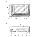
図2は、従来の表示装置であり、50は素子基板、51はTFTや素子を有する駆動回路部や画素部などの素子部、53は乾燥剤、54はシール材、55は乾燥剤53を設置する凹部、60は封止基板である。
FIG. 2 shows a conventional display device, in which 50 is an element substrate, 51 is an element portion such as a driving circuit portion or a pixel portion having TFTs and elements, 53 is a desiccant, 54 is a sealant, and 55 is a desiccant 53. The
図2に示す従来の表示装置は、乾燥剤53を設置するために、封止基板60を加工し、凹部55を形している。この凹部55は、ブラスト加工法、ミル加工等の機械加工法、ガラス基板を溶かす化学的加工法などで形成される。ブラスト加工法は、サンドブラスト法などの、砂等の砥粒を衝突させることによる加工方法である。これらの方法は作製工程において、ゴミや重金属汚染等の問題があり、その洗浄方法を含めて対応する必要がある。また、機械加工等では凹部がすりガラス状になったり、凹凸が存在するため、光の取り出し効率を低下させるので、上面出射型、両面出射型の表示装置には不適当である。光の取り出し効率とは、素子の発光に対して素子の基板正面から大気中に放出される発光の割合である。
In the conventional display device shown in FIG. 2, in order to install the
従来の方法では、このように封止基板に、凹部を形成する加工工程が必要となり、工程に必要な装置も増加し、工程が複雑化する。封止基板への加工工程によるダメージ(損傷)も生じる可能性があり、表面が疎面化し平坦性が損なわれることにより透光性が低下したり、薄型な封止基板では破損したりする恐れがある。また封止基板に設けるように凹部を素子基板へ形成することは困難であり、乾燥剤を設ける場所に制限がある。
本発明は、発光素子の劣化を防ぐことのできる信頼性の高い表示装置、及びその表示装置をより簡略に作製できる作製方法を提供することを目的とする。 An object of the present invention is to provide a highly reliable display device capable of preventing deterioration of a light emitting element and a manufacturing method capable of manufacturing the display device more simply.
本発明の表示装置の一は、一対の基板と、発光素子と、吸湿性物質を含む層と、枠体とを有し、枠体は吸湿性物質を含む層を囲んで設けられ、発光素子と、吸湿性物質を含む層と枠体とを内側に封じ込めるように、一対の基板は固着される。 One display device of the present invention includes a pair of substrates, a light-emitting element, a layer containing a hygroscopic substance, and a frame, and the frame is provided to surround the layer containing the hygroscopic substance. The pair of substrates are fixed so that the layer containing the hygroscopic substance and the frame body are enclosed inside.
本発明の表示装置の一は、発光素子が設けられた画素部を有する第1の基板と、第2の基板と、吸湿性物質を含む層と、画素部を囲む枠体とを有し、吸湿性物質を含む層は枠体に囲まれて設けられ、第1の基板と第2の基板とは、画素部と、吸湿性物質を含む層と、枠体とを内側に封じ込めるように、シール材によって固着される。 One of the display devices of the present invention includes a first substrate having a pixel portion provided with a light emitting element, a second substrate, a layer containing a hygroscopic substance, and a frame surrounding the pixel portion. The layer containing the hygroscopic substance is provided surrounded by the frame body, and the first substrate and the second substrate are formed so that the pixel portion, the layer containing the hygroscopic substance, and the frame body are enclosed inside. It is fixed by a sealing material.
本発明の表示装置の一は、発光素子が設けられた画素部と駆動回路からなる回路部とを有する第1の基板と、第2の基板と、吸湿性物質を含む層と、画素部を囲む枠体と、画素部と回路部とを囲むシール材とを有し、吸湿性物質を含む層は枠体とシール材との間に設けられ、第1の基板と第2の基板とは、画素部と、回路部と、吸湿性物質を含む層と、枠体とを内側に封じ込めるように、シール材によって固着される。 One embodiment of the display device of the present invention includes a first substrate having a pixel portion provided with a light-emitting element and a circuit portion including a driver circuit, a second substrate, a layer containing a hygroscopic substance, and a pixel portion. An enclosing frame, and a sealant enclosing the pixel portion and the circuit portion, and the layer containing a hygroscopic substance is provided between the frame and the sealant, and the first substrate and the second substrate are The pixel portion, the circuit portion, the layer containing a hygroscopic substance, and the frame body are fixed by a sealing material so as to be contained inside.
本発明の表示装置の一は、発光素子が設けられた画素部と駆動回路からなる回路部とを有する第1の基板と、第2の基板と、吸湿性物質を含む層と、画素部と回路部の一部とを囲む枠体とを有し、吸湿性物質を含む層は枠体に囲まれて設けられ、第1の基板と第2の基板とは、画素部と、回路部と、吸湿性物質を含む層と、枠体とを内側に封じ込めるように、シール材によって固着される。 According to one embodiment of the display device of the present invention, a first substrate having a pixel portion provided with a light emitting element and a circuit portion including a driver circuit, a second substrate, a layer containing a hygroscopic substance, a pixel portion, A layer surrounding a part of the circuit portion, the layer containing a hygroscopic substance is provided surrounded by the frame, and the first substrate and the second substrate include a pixel portion, a circuit portion, The layer containing the hygroscopic substance and the frame are fixed by a sealing material so as to be contained inside.
本発明の表示装置の一は、発光素子が設けられた画素部と駆動回路からなる回路部とを有する第1の基板と、第2の基板と、吸湿性物質を含む層と、画素部と回路部とを囲む枠体とを有し、吸湿性物質を含む層は枠体に囲まれて設けられ、第1の基板と第2の基板とは、画素部と、回路部と、吸湿性物質を含む層と、枠体とを内側に封じ込めるように、シール材によって固着される。 According to one embodiment of the display device of the present invention, a first substrate having a pixel portion provided with a light emitting element and a circuit portion including a driver circuit, a second substrate, a layer containing a hygroscopic substance, a pixel portion, And a layer including a hygroscopic substance is provided so as to be surrounded by the frame, and the first substrate and the second substrate include a pixel portion, a circuit portion, and a hygroscopic property. The layer including the substance and the frame are fixed by a sealing material so as to be contained inside.
本発明の表示装置の一は、発光素子が設けられた画素部と駆動回路からなる回路部とを有する第1の基板と、第2の基板と、吸湿性物質を含む層と、回路部を囲む枠体とを有し、吸湿性物質を含む層は枠体に囲まれて設けられ、第1の基板と第2の基板とは、画素部と、回路部と、吸湿性物質を含む層と、枠体とを内側に封じ込めるように、シール材によって固着される。 One embodiment of the display device of the present invention includes a first substrate having a pixel portion provided with a light-emitting element and a circuit portion including a driver circuit, a second substrate, a layer containing a hygroscopic substance, and a circuit portion. And a layer containing a hygroscopic substance is provided surrounded by the frame, and the first substrate and the second substrate are a pixel portion, a circuit portion, and a layer containing a hygroscopic substance. Then, it is fixed by a sealing material so as to contain the frame body inside.
本発明の表示装置の一は、発光素子が設けられた画素部と駆動回路からなる回路部とを有する第1の基板と、第2の基板と、吸湿性物質を含む層と、画素部と回路部とを囲む第1の枠体と、画素部を囲む第2の枠体とを有し、吸湿性物質を含む層は第1の枠体と第2の枠体との間に設けられ、第1の基板と、第2の基板は、画素部と、回路部と、吸湿性物質を含む層と、第1の枠体と、第2の枠体とを内側に封じ込めるように、シール材によって固着される。 According to one embodiment of the display device of the present invention, a first substrate having a pixel portion provided with a light emitting element and a circuit portion including a driver circuit, a second substrate, a layer containing a hygroscopic substance, a pixel portion, The first frame body surrounding the circuit portion and the second frame body surrounding the pixel portion are provided, and the layer containing the hygroscopic substance is provided between the first frame body and the second frame body. The first substrate and the second substrate are sealed so that the pixel portion, the circuit portion, the layer containing a hygroscopic substance, the first frame body, and the second frame body are sealed inside. It is fixed by the material.
本発明の表示装置の作製方法の一は、第1の基板上に発光素子を形成し、発光素子を囲んで枠体を形成し、枠体で囲まれた領域に、液状の吸湿性物質を含む組成物を滴下し、組成物を固化することにより吸湿性物質を含む層を形成し、発光素子と吸湿性物質を含む層と、枠体とを内側に封じ込めるように、第1の基板と第2の基板とをシール材によって固着する。 According to one method for manufacturing a display device of the present invention, a light-emitting element is formed over a first substrate, a frame is formed around the light-emitting element, and a liquid hygroscopic substance is formed in a region surrounded by the frame. A first substrate so as to form a layer containing a hygroscopic substance by dripping the composition containing the composition and solidifying the composition, and to enclose the light emitting element, the layer containing the hygroscopic substance, and the frame inside; The second substrate is fixed with a sealing material.
本発明の表示装置の作製方法の一は、第1の基板上に発光素子と駆動回路とを形成し、駆動回路を囲んで枠体を形成し、発光素子と駆動回路とを囲んでシール材を形成し、枠体とシール材との間に、液状の吸湿性物質を含む組成物を滴下し、組成物を固化することにより吸湿性物質を含む層を形成し、発光素子と、駆動回路と、吸湿性物質を含む層と、枠体とを内側に封じ込めるように、第1の基板と第2の基板とをシール材によって固着する。 According to one embodiment of the method for manufacturing a display device of the present invention, a light emitting element and a driving circuit are formed over a first substrate, a frame is formed around the driving circuit, and a sealing material is surrounded by the light emitting element and the driving circuit. Forming a layer containing a hygroscopic substance by dripping a composition containing a liquid hygroscopic substance between the frame and the sealing material, and solidifying the composition; and a light emitting element and a driving circuit In addition, the first substrate and the second substrate are fixed with a sealing material so that the layer containing the hygroscopic substance and the frame body are enclosed inside.
本発明の表示装置の作製方法の一は、第1の基板上に発光素子と駆動回路とを形成し、発光素子と駆動回路とを囲んで枠体を形成し、枠体で囲まれた領域に、液状の吸湿性物質を含む組成物を滴下し、組成物を固化することにより吸湿性物質を含む層を形成し、発光素子と、駆動回路と、吸湿性物質を含む層と、枠体とを内側に封じ込めるように、第1の基板と第2の基板とをシール材によって固着する。 In one embodiment of the method for manufacturing a display device of the present invention, a light-emitting element and a driver circuit are formed over a first substrate, a frame body is formed to surround the light-emitting element and the driver circuit, and a region surrounded by the frame body A layer containing a hygroscopic substance is formed by dripping a composition containing a liquid hygroscopic substance and solidifying the composition, and a light emitting element, a drive circuit, a layer containing the hygroscopic substance, and a frame The first substrate and the second substrate are fixed with a sealing material so as to be sealed inside.
本発明の表示装置の作製方法の一は、第1の基板上に発光素子と駆動回路とを形成し、駆動回路を囲んで枠体を形成し、枠体で囲まれた領域に、液状の吸湿性物質を含む組成物を滴下し、組成物を固化することにより吸湿性物質を含む層を形成し、発光素子と、駆動回路と、吸湿性物質を含む層と、枠体とを内側に封じ込めるように、第1の基板と第2の基板とをシール材によって固着する。 According to one embodiment of the method for manufacturing a display device of the present invention, a light emitting element and a driver circuit are formed over a first substrate, a frame body is formed around the driver circuit, and a liquid crystal is formed in a region surrounded by the frame body. A composition containing a hygroscopic substance is dropped, and a layer containing the hygroscopic substance is formed by solidifying the composition, and the light emitting element, the driving circuit, the layer containing the hygroscopic substance, and the frame are placed inside. The first substrate and the second substrate are fixed with a sealing material so as to be sealed.
本発明の表示装置の作製方法の一は、第1の基板上に発光素子と駆動回路とを形成し、発光素子と駆動回路とを囲んで第1の枠体を形成し、発光素子を囲んで第2の枠体を形成し、第1の枠体と第2の枠体との間に、液状の吸湿性物質を含む組成物を滴下し、組成物を固化することにより吸湿性物質を含む層を形成し、発光素子と、駆動回路と、吸湿性物質を含む層と、第1の枠体と、第2の枠体とを内側に封じ込めるように、第1の基板と第2の基板とをシール材によって固着する。 According to one embodiment of the method for manufacturing a display device of the present invention, a light emitting element and a driver circuit are formed over a first substrate, a first frame is formed surrounding the light emitting element and the driver circuit, and the light emitting element is surrounded. The second frame is formed, and a composition containing a liquid hygroscopic substance is dropped between the first frame and the second frame, and the composition is solidified to obtain the hygroscopic substance. Forming a layer including the first substrate and the second substrate so as to enclose the light emitting element, the driving circuit, the layer including the hygroscopic substance, the first frame, and the second frame. The substrate is fixed with a sealing material.
本発明により、光取り出し効率を低下することなく、広範囲に吸湿性物質を含む層からなる乾燥剤が設けられた表示装置を作製することができるので、乾燥剤の十分な吸湿効果により発光素子の劣化を防止することができる。また、複雑な作製工程も必要としない。従って、高繊細で、高品質な画像を表示できる、信頼性の高い表示装置を歩留まりよく作製することができる。 According to the present invention, it is possible to manufacture a display device provided with a desiccant composed of a layer containing a hygroscopic substance in a wide range without reducing light extraction efficiency. Deterioration can be prevented. Further, a complicated manufacturing process is not required. Therefore, a highly reliable display device that can display a high-definition and high-quality image can be manufactured with high yield.
(実施の形態1)
本発明の実施の形態について、図面を用いて詳細に説明する。但し、本発明は以下の説明に限定されず、本発明の趣旨及びその範囲から逸脱することなくその形態及び詳細を様々に変更し得ることは当業者であれば容易に理解される。従って、本発明は以下に示す実施の形態の記載内容に限定して解釈されるものではない。なお、以下に説明する本発明の構成において、同一部分又は同様な機能を有する部分には同一の符号を異なる図面間で共通して用い、その繰り返しの説明は省略する。
(Embodiment 1)
Embodiments of the present invention will be described in detail with reference to the drawings. However, the present invention is not limited to the following description, and it is easily understood by those skilled in the art that modes and details can be variously changed without departing from the spirit and scope of the present invention. Therefore, the present invention should not be construed as being limited to the description of the embodiments below. Note that in structures of the present invention described below, the same portions or portions having similar functions are denoted by the same reference numerals in different drawings, and description thereof is not repeated.
図16は本発明に係る表示パネルの構成を示す上面図であり、絶縁表面を有する基板2700上に画素2702をマトリクス上に配列させた画素部2701、走査線側入力端子2703、信号線側入力端子2704が形成されている。画素数は種々の規格に従って設ければ良く、XGAであれば1024×768×3(RGB)、UXGAであれば1600×1200×3(RGB)、フルスペックハイビジョンに対応させるのであれば1920×1080×3(RGB)とすれば良い。
FIG. 16 is a top view showing a structure of a display panel according to the present invention. A
画素2702は、走査線側入力端子2703から延在する走査線と、信号線側入力端子2704から延在する信号線とが交差することで、マトリクス状に配設される。画素2702のそれぞれには、スイッチング素子とそれに接続する画素電極が備えられている。スイッチング素子の代表的な一例はTFTであり、TFTのゲート電極側が走査線と、ソース若しくはドレイン側が信号線と接続されることにより、個々の画素を外部から入力する信号によって独立して制御可能としている。
The
TFTは、その主要な構成要素として、半導体層、ゲート絶縁層及びゲート電極層が挙げられ、半導体層に形成されるソース及びドレイン領域に接続する配線層がそれに付随する。構造的には基板側から半導体層、ゲート絶縁層及びゲート電極層を配設したトップゲート型と、基板側からゲート電極層、ゲート絶縁層及び半導体層を配設したボトムゲート型などが代表的に知られているが、本発明においてはそれらの構造のどのようなものを用いても良い。 A TFT includes a semiconductor layer, a gate insulating layer, and a gate electrode layer as main components, and a wiring layer connected to a source region and a drain region formed in the semiconductor layer is attached to the TFT. Structurally, the top gate type in which the semiconductor layer, the gate insulating layer and the gate electrode layer are arranged from the substrate side, and the bottom gate type in which the gate electrode layer, the gate insulating layer and the semiconductor layer are arranged from the substrate side are representative. In the present invention, any of those structures may be used.
半導体層を形成する材料は、シランやゲルマンに代表される半導体材料ガスを用いて気相成長法やスパッタリング法で作製されるアモルファス半導体(以下「AS」ともいう。)、該非晶質半導体を光エネルギーや熱エネルギーを利用して結晶化させた多結晶半導体、或いはセミアモルファス(微結晶若しくはマイクロクリスタルとも呼ばれる。以下「SAS」ともいう。)半導体などを用いることができる。 As a material for forming the semiconductor layer, an amorphous semiconductor (hereinafter also referred to as “AS”) manufactured by a vapor deposition method or a sputtering method using a semiconductor material gas typified by silane or germane is used. A polycrystalline semiconductor crystallized using energy or thermal energy, a semi-amorphous (also referred to as microcrystal or microcrystal, hereinafter, also referred to as “SAS”) semiconductor, or the like can be used.
SASは、非晶質と結晶構造(単結晶、多結晶を含む)の中間的な構造を有し、自由エネルギー的に安定な第3の状態を有する半導体であって、短距離秩序を持ち格子歪みを有する結晶質な領域を含んでいる。少なくとも膜中の一部の領域には、0.5〜20nmの結晶領域を観測することが出来、珪素を主成分とする場合にはラマンスペクトルが520cm-1よりも低波数側にシフトしている。X線回折では珪素結晶格子に由来するとされる(111)、(220)の回折ピークが観測される。未結合手(ダングリングボンド)の中和剤として水素またはハロゲンを少なくとも1原子%またはそれ以上含ませている。SASは、珪化物気体をグロー放電分解(プラズマCVD)して形成する。珪化物気体としては、SiH4、その他にもSi2H6、SiH2Cl2、SiHCl3、SiCl4、SiF4などを用いることが可能である。またGeF4を混合させても良い。この珪化物気体をH2、又は、H2とHe、Ar、Kr、Neから選ばれた一種または複数種の希ガス元素で希釈しても良い。希釈率は2〜1000倍の範囲。圧力は概略0.1Pa〜133Paの範囲、電源周波数は1MHz〜120MHz、好ましくは13MHz〜60MHz。基板加熱温度は300℃以下でよい。膜中の不純物元素として、酸素、窒素、炭素などの大気成分の不純物は1×1020cm-3以下とすることが望ましく、特に、酸素濃度は5×1019/cm3以下、好ましくは1×1019/cm3以下とする。 SAS is a semiconductor having an intermediate structure between amorphous and crystalline structures (including single crystal and polycrystal) and having a third state that is stable in terms of free energy and has a short-range order and a lattice. It includes a crystalline region with strain. A crystal region of 0.5 to 20 nm can be observed in at least a part of the film, and when silicon is the main component, the Raman spectrum shifts to a lower wave number side than 520 cm −1. Yes. In X-ray diffraction, diffraction peaks of (111) and (220) that are derived from the silicon crystal lattice are observed. At least 1 atomic% or more of hydrogen or halogen is contained as a neutralizing agent for dangling bonds. The SAS is formed by glow discharge decomposition (plasma CVD) of a silicide gas. As the silicide gas, SiH 4 , Si 2 H 6 , SiH 2 Cl 2 , SiHCl 3 , SiCl 4 , SiF 4, and the like can be used. Further, GeF 4 may be mixed. This silicide gas may be diluted with H 2 , or H 2 and one or more kinds of rare gas elements selected from He, Ar, Kr, and Ne. The dilution rate is in the range of 2 to 1000 times. The pressure is generally in the range of 0.1 Pa to 133 Pa, and the power supply frequency is 1 MHz to 120 MHz, preferably 13 MHz to 60 MHz. The substrate heating temperature may be 300 ° C. or less. As an impurity element in the film, impurities of atmospheric components such as oxygen, nitrogen, and carbon are desirably 1 × 10 20 cm −3 or less, and in particular, the oxygen concentration is 5 × 10 19 / cm 3 or less, preferably 1 × 10 19 / cm 3 or less
図16は、走査線及び信号線へ入力する信号を、外付けの駆動回路により制御する表示パネルの構成を示しているが、図17に示すように、COG(Chip on Glass)によりドライバIC755a、755b、757a、757b、757cを基板750上に実装しても良い。ドライバICは単結晶半導体基板に形成されたものでも良いし、ガラス基板上にTFTで回路を形成したものであっても良い。図17において、751は画素部であり、基板750は封止基板753とシール材752で固着されている。ドライバIC755a、755b、757a、757b、757cは基板750上にCOGにより実装され、FPC756a、756b、754a、754b、754cに接続している。
FIG. 16 shows a configuration of a display panel in which signals input to the scanning lines and signal lines are controlled by an external drive circuit. As shown in FIG. 17, a
また、画素に設けるTFTをSASで形成する場合には、図18に示すように走査線側駆動回路3702を基板3700上に形成し一体化することも出来る。図18において、3701は画素部であり、信号線側駆動回路は、COGによりドライバIC3705a、3705bを実装し、FPC3704a、3704bに接続している。
In the case where a TFT provided for a pixel is formed using SAS, a scan line
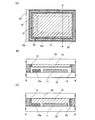
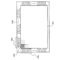
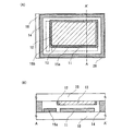
本発明の実施の形態について、図1を用いて説明する。図1(A)は表示装置の上面図であり、図1(B)、(C)は、図1(A)において、線A−A'による断面図である。また図1(B)、図1(C)は枠体と吸湿性物質を含む層の形状が異なっている例である。 An embodiment of the present invention will be described with reference to FIG. 1A is a top view of the display device, and FIGS. 1B and 1C are cross-sectional views taken along line AA ′ in FIG. 1B and 1C are examples in which the shape of the frame and the layer containing the hygroscopic substance are different.
本発明は、表示装置内に吸湿性物質を含む層を形成する際に、滴下方法を用いることを特徴とする。吸湿性物質は、空気など雰囲気中の水分を吸収する性質を有る物質であり、表示装置内に設けられることで、発光素子を劣化させる水分を吸収する効果がある。吸湿性物質が乾燥剤として機能するので、発光素子の劣化を防ぎ、表示装置の信頼性を向上させる。本発明では、封止基板、または素子基板に吸湿性物質を固定し、吸湿性物質を含む層を形成する際に、液状の吸湿性物質を有する組成物の状態で滴下する。液状の吸湿性物質を含む組成物は、例えば、吸湿性物質を固定材となる物質に溶解した、または分散させたものでもよい。その際、滴下する領域を定めるために、封止基板、または素子基板上にあらかじめ枠体を形成する。枠体は閉じられた形状を有しており、前記枠体内に吸湿性物質は滴下される。 The present invention is characterized in that a dropping method is used when a layer containing a hygroscopic substance is formed in a display device. The hygroscopic substance is a substance that has a property of absorbing moisture in an atmosphere such as air, and has an effect of absorbing moisture that deteriorates the light-emitting element by being provided in the display device. Since the hygroscopic substance functions as a desiccant, deterioration of the light emitting element is prevented and the reliability of the display device is improved. In the present invention, when a hygroscopic substance is fixed to a sealing substrate or an element substrate and a layer containing the hygroscopic substance is formed, it is dropped in the state of a composition having a liquid hygroscopic substance. The composition containing a liquid hygroscopic substance may be, for example, a solution obtained by dissolving or dispersing the hygroscopic substance in a substance serving as a fixing material. At that time, in order to determine a region to be dropped, a frame body is formed in advance on the sealing substrate or the element substrate. The frame has a closed shape, and the hygroscopic substance is dropped into the frame.
図1は、本発明の表示装置の一例であり、10は素子基板、11は画素部、15a、15bは駆動回路部、12は枠体、13は吸湿性物質を含む層、14はシール材、20は封止基板である。 FIG. 1 shows an example of a display device according to the present invention, in which 10 is an element substrate, 11 is a pixel portion, 15a and 15b are drive circuit portions, 12 is a frame body, 13 is a layer containing a hygroscopic substance, and 14 is a sealing material. , 20 is a sealing substrate.
本発明の表示装置は、図1に示すように、封止基板に凹部を形成せず、枠体12を画素部11、及び駆動回路部15a、15bを囲むように形成し、その囲まれた枠体の中に、透光性を有する吸湿性物質を含む層13が充填されるように形成されている。なお、素子基板10には、画素部11、駆動回路部15a、駆動回路部15bなどの素子部が形成されている。本実施の形態においては、枠体12は画素部11、及び駆動回路部15a、駆動回路部15bの形成領域を囲むように形成するので、吸湿性物質を含む層13を広面積にわたって形成でき、広い面積で水分を吸収できるので、乾燥効率が高い。本発明の表示装置は、選択的に枠体12を形成すれば、所望の場所に簡単に乾燥剤として機能する吸湿性物質を含む層を設けることができる。本発明の吸湿性物質を含む層の形成方法を図3に示す。
In the display device of the present invention, as shown in FIG. 1, the
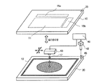
図3は、本発明に適用できる吸湿性物質の滴下装置の一態様であり、40は滴下制御回路、42はCCDなどの撮像手段、45はマーカー、43はヘッドである。滴下制御回路40により、滴下ヘッド43のノズルより液状の吸湿性物質を含む組成物17を封止基板20へ滴下する。封止基板20には、液状の吸湿性物質を含む組成物17の領域を決定するための、枠体12を形成する。その枠体12によって囲まれた領域に液状の吸湿性物質を含む組成物17を滴下し、焼成等の乾燥の後、吸湿性物質を含む層が形成される。本実施の形態のように液状の吸湿性物質を含む組成物を、枠体12内に滴下することもできるが、液状の組成物は閉じられた形状の領域に滴下すればよいので、枠体とシール材によって囲まれた領域などにも滴下し、乾燥剤となる吸湿性物質を含む層を形成することができる。また、枠体及び吸湿性物質を含む層は素子基板側でも封止基板側でもどちらにも形成することができる。また、枠体の大きさや高さによって吸湿性物質を含む層の形状は、どのようにも設計することができる。図1の(B)の表示装置では、枠体12を封止基板20上にシール材の高さより低く形成し、その枠体内に吸湿性物質を含む層を形成しているため、素子基板の素子部に接しないで形成されている。しかし、図1(C)のように枠体の高さとシール材の高さを同等にすると、吸湿性物質を含む層13は素子部を直接覆うように形成することができる。この場合、枠体は素子基板側でも封止基板側でもどちらに形成してもよく、枠体や吸湿性物質を含む層を、封止基板と素子基板によってプレスし、平坦化することもできる。
FIG. 3 shows one aspect of a hygroscopic substance dropping apparatus applicable to the present invention, wherein 40 is a dropping control circuit, 42 is an imaging means such as a CCD, 45 is a marker, and 43 is a head. The dropping
また、滴下法のほかに、ディスペンサ法、液滴吐出法、スクリーン印刷法などの印刷法によって、液状の吸湿性物質を含む組成物を、基板上に形成してもよい。本実施の形態では、微少量の制御がしやすい滴下法を中心に述べた。滴下する工程を、窒素やアルゴン(Ar)等の不活性気体雰囲気中、もしくは減圧下で行うことが好ましい。減圧下で組成物の滴下を行うことによって、組成物中の水分が取り除けやすく固化する工程が簡略化する、組成物中の粘度が下がるので均一に広がりやすい、といった効果がある。 In addition to the dropping method, a composition containing a liquid hygroscopic substance may be formed on the substrate by a printing method such as a dispenser method, a droplet discharge method, or a screen printing method. In the present embodiment, the dropping method that can easily control a minute amount has been mainly described. The dropping step is preferably performed in an inert gas atmosphere such as nitrogen or argon (Ar) or under reduced pressure. By dropping the composition under reduced pressure, there is an effect that the process of solidifying the water in the composition is simplified, and the viscosity in the composition is lowered, so that the composition is easily spread uniformly.
枠体は、酸化珪素、窒化珪素、酸化窒化珪素、酸化アルミニウム、窒化アルミニウム、酸化窒化アルミニウムその他の無機材料でも、アクリル酸、メタクリル酸及びこれらの誘導体、又はポリイミド(polyimide)、芳香族ポリアミド、ポリベンゾイミダゾール(polybenzimidazole)、ベンゾシクロブテン、パリレン、フレア、エポキシなどの有機材料又はシロキサン系材料を出発材料として形成された珪素、酸素、水素からなる化合物のうちSi−O−Si結合を含む無機シロキサン、珪素上の水素がメチルやフェニルのような有機基によって置換された有機シロキサン系の材料で形成することができる。液状の吸湿性物質を含む層の枠体部になる手段であるので、金属などの導電材料でも、樹脂などの絶縁材料でもよい。樹脂材料としては、エポキシ樹脂、アクリル樹脂、フェノール樹脂、ノボラック樹脂、ポリイミドアミド樹脂、メラミン樹脂、ウレタン樹脂等の樹脂材料などを用いることができる。上記樹脂において、感光性アクリル、感光性ポリイミドなどの感光性な物質、非感光性アクリル、非感光性ポリイミドなど非感光性の物質どちらも用いることができる。或いは、感光剤を含む市販のレジスト材料を用いてもよく、例えば、代表的なポジ型レジストである、ノボラック樹脂と感光剤であるナフトキノンジアジド化合物、ネガ型レジストであるベース樹脂、ジフェニルシランジオール及び酸発生剤などを用いてもよい。 The frame is made of silicon oxide, silicon nitride, silicon oxynitride, aluminum oxide, aluminum nitride, aluminum oxynitride, or other inorganic materials such as acrylic acid, methacrylic acid and derivatives thereof, polyimide, aromatic polyamide, poly Inorganic siloxanes containing Si-O-Si bonds among organic compounds such as benzimidazole (polybenzimidazole), benzocyclobutene, parylene, flare, epoxy, etc., and compounds composed of silicon, oxygen and hydrogen formed from siloxane-based materials It can be formed of an organosiloxane material in which the hydrogen on silicon is replaced by an organic group such as methyl or phenyl. Since it is a means for forming a frame portion of a layer containing a liquid hygroscopic substance, it may be a conductive material such as metal or an insulating material such as resin. As the resin material, an epoxy resin, an acrylic resin, a phenol resin, a novolac resin, a polyimide amide resin, a melamine resin, a urethane resin, or the like can be used. In the above resin, any of photosensitive materials such as photosensitive acrylic and photosensitive polyimide, and non-photosensitive materials such as non-photosensitive acrylic and non-photosensitive polyimide can be used. Alternatively, a commercially available resist material containing a photosensitizer may be used. For example, a novolak resin that is a typical positive resist and a naphthoquinonediazide compound that is a photosensitizer, a base resin that is a negative resist, diphenylsilanediol, and An acid generator or the like may be used.
いずれの材料も所望の形状の閉じられた枠状のパターンに形成する。もしくはシール材と接して形成し、閉じられた枠状のパターンを形成する。パターニングは、ドライエッチング、またはウェットエッチング、アッシングなどによって行うことができる。また、レジストや感光性アクリルなどの感光性な物質を枠体として用いる場合は、パターニングの際にレジスト等のマスクを用いなくても良いため、工程が簡略化する。非感光性の物質の場合はレジスト等のマスクを用いてドライエッチング、アッシングによってパターンを形成すればよい。また、ディスペンサ法、液滴吐出法、スクリーン印刷法などの印刷法によって、直接基板上に枠体を形成してもよく、パターニングの工程を必要としないため工程が簡略化する。 Both materials are formed into a closed frame-like pattern having a desired shape. Or it forms in contact with a sealing material and forms a closed frame-like pattern. Patterning can be performed by dry etching, wet etching, ashing, or the like. In the case where a photosensitive substance such as a resist or photosensitive acrylic is used as the frame, the process is simplified because a mask such as a resist is not required for patterning. In the case of a non-photosensitive substance, a pattern may be formed by dry etching or ashing using a mask such as a resist. In addition, the frame body may be formed directly on the substrate by a printing method such as a dispenser method, a droplet discharge method, or a screen printing method, and the patterning step is not required, thereby simplifying the process.
また、枠体をシール材と同材料によって形成してもよい。シール材としては、例えばビスフェノールA型液状樹脂、ビスフェノールA型固形樹脂、含ブロムエポキシ樹脂、ビスフェノールF型樹脂、ビスフェノールAD型樹脂、フェノール型樹脂、クレゾール型樹脂、ノボラック型樹脂、環状脂肪族エポキシ樹脂、エピビス型エポキシ樹脂、グリシジルエステル樹脂、グリジシルアミン系樹脂、複素環式エポキシ樹脂、変性エポキシ樹脂等のエポキシ樹脂を用いることができる。 Moreover, you may form a frame with the same material as a sealing material. Examples of the sealing material include bisphenol A type liquid resin, bisphenol A type solid resin, bromine-containing epoxy resin, bisphenol F type resin, bisphenol AD type resin, phenol type resin, cresol type resin, novolac type resin, and cyclic aliphatic epoxy resin. An epoxy resin such as an epibis type epoxy resin, a glycidyl ester resin, a glycidylamine resin, a heterocyclic epoxy resin, or a modified epoxy resin can be used.
吸湿性物質は、流動性を有し滴下可能な液状の状態、つまり液体の状態、または他の溶媒に溶解した状態で、滴下され、枠体内に滴下された後、焼成、乾燥等によって固化し形成される。ここでいう固化とは、流動性を失うことを意味する。よって吸湿性物質は、滴下後、基板上に固定された状態で、吸湿性を有していればよい。基板に固定された状態とは、基板上に固定して形成されていればよく、流動性を失ったゲル状のものであってもよい。 The hygroscopic substance is in a liquid state that can be dripped, that is, in a liquid state, that is, in a liquid state or in a state dissolved in another solvent, dropped into the frame, and then solidified by baking, drying, or the like. It is formed. Solidification here means loss of fluidity. Therefore, the hygroscopic substance only needs to have hygroscopicity after being dropped and fixed on the substrate. The state fixed to the substrate may be formed on the substrate as long as it is fixed, and may be a gel-like material that loses fluidity.
透光性を有する吸湿性物質を含む層を用いる場合は、封止基板側から光を取り出す構造の表示装置でも、光の取り出し効率を減少することがない。この透光性は、表示装置内の乾燥剤として用いる完成形態、つまり、流動性を失った状態のとき有していればよく、滴下するときの流動性を有する液状の状態の時に、不透光性であっても構わない。例えば、不透光性の溶媒に溶解した組成物の状態で滴下する物質でも、滴下後の焼成によって、溶媒が揮発し、最終的に乾燥剤として封止基板に設けられる吸湿性物質が透光性であれば用いることができる。 In the case of using a layer containing a light-transmitting hygroscopic substance, the light extraction efficiency is not reduced even in a display device having a structure in which light is extracted from the sealing substrate side. This translucency is sufficient when it is in a completed form used as a desiccant in the display device, that is, when it loses fluidity, and when it is in a liquid state with fluidity when dropped. It may be light. For example, even in the case of a substance that is dropped in the state of a composition dissolved in a non-translucent solvent, the solvent is volatilized by baking after dropping, and the hygroscopic substance that is finally provided on the sealing substrate as a desiccant is translucent. Any sex can be used.
図2で示す従来の表示装置のように、画素部の上部に、透光性を有しない固体の乾燥剤53が設けられていると、封止基板側からの光の取り出し効率が低下する。そのため画素部を除いて乾燥剤を設けると、表示装置の筐体が大型化してしまい、乾燥剤を設置する範囲を狭めると、十分な乾燥剤の吸収効果が減少してしまう。また凹部により発光層と基板との距離が表示装置内で一定にならないので、表示画像にばらつきやムラが生じる可能性がある。
As in the conventional display device shown in FIG. 2, when a
本実施の形態の吸湿性物質を含む層は透光性を有している。透光性を有する吸湿性物質を含む層を用いるため、封止基板側から光を取り出す上面出射型、両面出射型の表示装置の画素部を覆うように形成しても、発光層からの光を遮断することはない。よって、吸湿性物質を表示装置内部の所望な場所に広範囲に形成することができるので、十分に吸収効果を発揮できる。また、封止基板に凹部を形成しないので、発光層と封止基板との間隔が一定であり、光の干渉などによる表示画像のばらつきやムラが生じない。 The layer containing a hygroscopic substance of this embodiment has a light-transmitting property. Since a layer containing a light-transmitting hygroscopic substance is used, light from the light-emitting layer can be formed even if it is formed so as to cover the pixel portion of a top emission type display device that takes out light from the sealing substrate side or a dual emission type display device. Never shut off. Therefore, since the hygroscopic substance can be formed over a wide range at a desired location inside the display device, the absorption effect can be sufficiently exhibited. In addition, since the concave portion is not formed in the sealing substrate, the distance between the light emitting layer and the sealing substrate is constant, and the display image does not vary or become uneven due to light interference or the like.
以上、本発明により、光取り出し効率を低下させることなく、広範囲に吸湿性物質が設けられた表示装置を作製することができるので、吸湿性物質の十分な吸湿効果により発光素子の劣化を防止することができる。また、複雑な作製工程も必要としない。従って、高繊細で、高品質な画像を表示できる、信頼性の高い表示装置を歩留まりよく作製することができる。 As described above, according to the present invention, a display device in which a hygroscopic substance is provided in a wide range can be manufactured without reducing light extraction efficiency. Therefore, deterioration of the light-emitting element is prevented by a sufficient hygroscopic effect of the hygroscopic substance. be able to. Further, a complicated manufacturing process is not required. Therefore, a highly reliable display device that can display a high-definition and high-quality image can be manufactured with high yield.
(実施の形態2)
本発明の表示装置の作製方法を、図4乃至図7を用いて詳細に説明する。
(Embodiment 2)
A method for manufacturing a display device of the present invention will be described in detail with reference to FIGS.
絶縁表面を有する基板100の上に下地膜101として、プラズマCVD法により窒化酸化珪素膜(SiNO)101aを10〜200nm(好ましくは50〜100nm)を形成し、酸化窒化珪素膜(SiON)101bを50〜200nm(好ましくは100〜150nm)積層する。基板100としてはガラス基板、石英基板やシリコン基板、金属基板またはステンレス基板の表面に絶縁膜を形成したものを用いても良い。また、本実施の形態の処理温度に耐えうる耐熱性を有するプラスチック基板を用いてもよいし、フィルムのような可撓性基板を用いても良い。また、下地膜として2層構造を用いてもよいし、前記下地(絶縁)膜の単層膜又は2層以上積層させた構造を用いてもよい。
A silicon nitride oxide film (SiNO) 101a having a thickness of 10 to 200 nm (preferably 50 to 100 nm) is formed as a base film 101 over a
次いで、下地膜上に半導体膜を形成する。半導体膜は25〜200nm(好ましくは30〜150nm)の厚さで公知の手段(スパッタ法、LPCVD法、またはプラズマCVD法等)により成膜すればよい。半導体膜の材料に限定はないが、好ましくはシリコン又はシリコンゲルマニウム(SiGe)合金などで形成すると良い。 Next, a semiconductor film is formed over the base film. The semiconductor film may be formed by a known means (a sputtering method, an LPCVD method, a plasma CVD method, or the like) with a thickness of 25 to 200 nm (preferably 30 to 150 nm). There is no limitation on the material of the semiconductor film, but it is preferably formed of silicon or a silicon germanium (SiGe) alloy.
半導体膜は、アモルファス半導体(代表的には水素化アモルファスシリコン)、結晶性半導体(代表的にはポリシリコン)を素材として用いている。ポリシリコンには、800℃以上のプロセス温度を経て形成される多結晶シリコンを主材料として用いた所謂高温ポリシリコンや、600℃以下のプロセス温度で形成される多結晶シリコンを主材料として用いた所謂低温ポリシリコン、また結晶化を促進する元素などを添加し結晶化させた結晶シリコンなどを含んでいる。 The semiconductor film uses an amorphous semiconductor (typically hydrogenated amorphous silicon) or a crystalline semiconductor (typically polysilicon) as a material. For polysilicon, so-called high-temperature polysilicon using polycrystalline silicon formed at a process temperature of 800 ° C. or higher as a main material, or polycrystalline silicon formed at a process temperature of 600 ° C. or lower as a main material is used. It includes so-called low-temperature polysilicon and crystalline silicon that is crystallized by adding an element that promotes crystallization.
また、他の物質として、セミアモルファス半導体又は半導体膜の一部に結晶相を含む半導体を用いることもできる。セミアモルファス半導体とは、非晶質と結晶構造(単結晶、多結晶を含む)の中間的な構造の半導体であり、自由エネルギー的に安定な第3の状態を有する半導体であって、短距離秩序を持ち格子歪みを有する結晶質なものである。典型的にはシリコンを主成分として含み、格子歪みを伴って、ラマンスペクトルが520cm-1よりも低波数側にシフトしている半導体膜である。また、未結合手(ダングリングボンド)の中和剤として水素またはハロゲンを少なくとも1原子%またはそれ以上含ませている。ここでは、このような半導体をセミアモルファス半導体(以下「SAS」と呼ぶ。)と呼ぶ。このSASは所謂微結晶(マイクロクリスタル)半導体(代表的には微結晶シリコン)とも呼ばれている。 As another substance, a semi-amorphous semiconductor or a semiconductor including a crystal phase in part of a semiconductor film can be used. A semi-amorphous semiconductor is a semiconductor having an intermediate structure between amorphous and crystalline (including single crystal and polycrystal), and has a third state that is stable in terms of free energy, and has a short distance. It is crystalline with order and lattice distortion. Typically, it is a semiconductor film containing silicon as a main component and having a Raman spectrum shifted to a lower wave number side than 520 cm −1 with lattice distortion. Further, hydrogen or halogen is contained at least 1 atomic% or more as a neutralizing agent for dangling bonds. Here, such a semiconductor is referred to as a semi-amorphous semiconductor (hereinafter referred to as “SAS”). This SAS is also called a so-called microcrystalline semiconductor (typically microcrystalline silicon).
このSASは珪化物気体をグロー放電分解(プラズマCVD)することにより得ることができる。代表的な珪化物気体としては、SiH4であり、その他にもSi2H6、SiH2Cl2、SiHCl3、SiCl4、SiF4などを用いることができる。また、GeF4、F2を混合してもよい。この珪化物気体を水素、若しくは水素とヘリウム、アルゴン、クリプトン、ネオンから選ばれた一種又は複数種の希ガス元素で希釈して用いることでSASの形成を容易なものとすることができる。珪化物気体に対する水素の希釈率は、例えば流量比で2倍〜1000倍とすることが好ましい。勿論、グロー放電分解によるSASの形成は、減圧下で行うことが好ましいが、大気圧における放電を利用しても形成することができる。代表的には、0.1Pa〜133Paの圧力範囲で行えば良い。グロー放電を形成するための電源周波数は1MHz〜120MHz、好ましくは13MHz〜60MHzである。高周波電力は適宜設定すれば良い。基板加熱温度は300℃以下が好ましく、100〜200℃の基板加熱温度でも形成可能である。ここで、主に成膜時に取り込まれる不純物元素として、酸素、窒素、炭素などの大気成分に由来する不純物は1×1020cm-3以下とすることが望ましく、特に、酸素濃度は5×1019cm-3以下、好ましくは1×1019cm-3以下となるようにすることが好ましい。また、ヘリウム、アルゴン、クリプトン、ネオンなどの希ガス元素を含ませて格子歪みをさらに助長させることで安定性が増し良好なSASが得られる。また半導体層としてフッ素系ガスより形成されるSAS層に水素系ガスより形成されるSAS層を積層してもよい。 This SAS can be obtained by glow discharge decomposition (plasma CVD) of a silicide gas. A typical silicide gas is SiH 4 , and in addition, Si 2 H 6 , SiH 2 Cl 2 , SiHCl 3 , SiCl 4 , SiF 4 and the like can be used. Further, GeF 4 and F 2 may be mixed. The formation of the SAS can be facilitated by diluting the silicide gas with one or plural kinds of rare gas elements selected from hydrogen or hydrogen and helium, argon, krypton, or neon. It is preferable that the dilution ratio of hydrogen with respect to the silicide gas is, for example, 2 to 1000 times in flow rate ratio. Of course, formation of the SAS by glow discharge decomposition is preferably performed under reduced pressure, but it can also be formed by utilizing discharge at atmospheric pressure. Typically, it may be performed in a pressure range of 0.1 Pa to 133 Pa. The power supply frequency for forming the glow discharge is 1 MHz to 120 MHz, preferably 13 MHz to 60 MHz. What is necessary is just to set high frequency electric power suitably. The substrate heating temperature is preferably 300 ° C. or lower, and can be formed even at a substrate heating temperature of 100 to 200 ° C. Here, as an impurity element mainly taken in at the time of film formation, it is desirable that impurities derived from atmospheric components such as oxygen, nitrogen, and carbon be 1 × 10 20 cm −3 or less, and in particular, the oxygen concentration is 5 × 10 5. It is preferable to be 19 cm −3 or less, preferably 1 × 10 19 cm −3 or less. Further, by adding a rare gas element such as helium, argon, krypton, or neon to further promote lattice distortion, stability is improved and a favorable SAS can be obtained. In addition, a SAS layer formed of a hydrogen-based gas may be stacked on a SAS layer formed of a fluorine-based gas as a semiconductor layer.
半導体膜に、結晶性半導体膜を用いる場合、その結晶性半導体膜の作製方法は、公知の方法(レーザー結晶化法、熱結晶化法、またはニッケルなどの結晶化を助長する元素を用いた熱結晶化法等)を用いれば良い。結晶化を助長する元素を導入しない場合は、非晶質珪素膜にレーザ光を照射する前に、窒素雰囲気下500℃で1時間加熱することによって非晶質珪素膜の含有水素濃度を1×10²⁰atoms/cm3以下にまで放出させる。これは水素を多く含んだ非晶質珪素膜にレーザ光を照射すると膜が破壊されてしまうからである。 In the case where a crystalline semiconductor film is used for the semiconductor film, a method for manufacturing the crystalline semiconductor film is a known method (laser crystallization method, thermal crystallization method, or heat using an element that promotes crystallization such as nickel. A crystallization method or the like may be used. In the case where an element for promoting crystallization is not introduced, the amorphous silicon film is heated at 500 ° C. for 1 hour in a nitrogen atmosphere before irradiating the amorphous silicon film with laser light, whereby the concentration of hydrogen contained in the amorphous silicon film is set to 1 ×. Release to 10 20 atoms / cm 3 or less. This is because the film is destroyed when the amorphous silicon film containing a large amount of hydrogen is irradiated with laser light.
非晶質半導体膜への金属元素の導入の仕方としては、当該金属元素を非晶質半導体膜の表面又はその内部に存在させ得る手法であれば特に限定はなく、例えばスパッタ法、CVD法、プラズマ処理法(プラズマCVD法も含む)、吸着法、金属塩の溶液を塗布する方法を使用することができる。このうち溶液を用いる方法は簡便であり、金属元素の濃度調整が容易であるという点で有用である。また、このとき非晶質半導体膜の表面の濡れ性を改善し、非晶質半導体膜の表面全体に水溶液を行き渡らせるため、酸素雰囲気中でのUV光の照射、熱酸化法、ヒドロキシラジカルを含むオゾン水又は過酸化水素による処理等により、酸化膜を成膜することが望ましい。 The method of introducing the metal element into the amorphous semiconductor film is not particularly limited as long as the metal element can be present on the surface of the amorphous semiconductor film or inside the amorphous semiconductor film. For example, sputtering, CVD, A plasma treatment method (including a plasma CVD method), an adsorption method, or a method of applying a metal salt solution can be used. Among these, the method using a solution is simple and useful in that the concentration of the metal element can be easily adjusted. At this time, in order to improve the wettability of the surface of the amorphous semiconductor film and to spread the aqueous solution over the entire surface of the amorphous semiconductor film, irradiation with UV light in an oxygen atmosphere, thermal oxidation method, hydroxy radical It is desirable to form an oxide film by treatment with ozone water or hydrogen peroxide.
また、非晶質半導体膜の結晶化は、熱処理とレーザ光照射による結晶化を組み合わせてもよく、熱処理やレーザ光照射を単独で、複数回行っても良い。熱処理とレーザ光照射の2段階で結晶化を行う場合、金属元素導入後に、500〜550℃で4〜20時間かけて熱処理を行い、非晶質半導体膜を結晶化する(以下、第1の結晶性半導体膜という。)。 In addition, the crystallization of the amorphous semiconductor film may be a combination of heat treatment and crystallization by laser light irradiation, or may be performed a plurality of times by heat treatment or laser light irradiation alone. When crystallization is performed in two stages of heat treatment and laser light irradiation, after introducing the metal element, the heat treatment is performed at 500 to 550 ° C. for 4 to 20 hours to crystallize the amorphous semiconductor film (hereinafter referred to as the first step). It is called a crystalline semiconductor film.)
次に第1の結晶性珪素膜にレーザ光を照射し結晶化を助長し、第2の結晶性半導体膜を得る。レーザ結晶化法は、レーザ光を半導体膜に照射する。用いるレーザは、パルス発振または連続発振の固体レーザ、気体レーザ、もしくは金属レーザが望ましい。なお、前記固体レーザとしてはYAGレーザ、YVO4レーザ、YLFレーザ、YAlO3レーザ、ガラスレーザ、ルビーレーザ、アレキサンドライドレーザ、Ti:サファイアレーザ等があり、前記気体レーザとしてはエキシマレーザ、Arレーザ、Krレーザ、CO2レーザ等があり、前記金属レーザとしてはヘリウムカドミウムレーザ、銅蒸気レーザ、金蒸気レーザが挙げられる。レーザビームは非線形光学素子により高調波に変換されていてもよい。前記非線形光学素子に使われる結晶は、例えばLBOやBBOやKDP、KTPやKB5、CLBOと呼ばれるものを使うと変換効率の点で優れている。これらの非線形光学素子をレーザの共振器の中に入れることで、変換効率を大幅に上げることができる。前記高調波のレーザには、一般にNd、Yb、Crなどがドープされており、これが励起しレーザが発振する。ドーパントの種類は適宜実施者が選択すればよい。 Next, the first crystalline silicon film is irradiated with laser light to promote crystallization, thereby obtaining a second crystalline semiconductor film. In the laser crystallization method, a semiconductor film is irradiated with laser light. The laser used is preferably a pulsed or continuous wave solid state laser, a gas laser, or a metal laser. The solid laser includes a YAG laser, a YVO 4 laser, a YLF laser, a YAlO 3 laser, a glass laser, a ruby laser, an alexandride laser, a Ti: sapphire laser, and the gas laser includes an excimer laser, an Ar laser, There are Kr laser, CO 2 laser, and the like, and examples of the metal laser include helium cadmium laser, copper vapor laser, and gold vapor laser. The laser beam may be converted into a harmonic by a non-linear optical element. Crystals used in the nonlinear optical element are excellent in terms of conversion efficiency when, for example, LBO, BBO, KDP, KTP, KB5, and CLBO are used. By introducing these nonlinear optical elements into the laser resonator, the conversion efficiency can be greatly increased. The harmonic laser is generally doped with Nd, Yb, Cr, etc., and this is excited to oscillate the laser. The practitioner may select the type of dopant as appropriate.
また、結晶性半導体層を、直接基板に線状プラズマ法により形成しても良い。また、線状プラズマ法を用いて、結晶性半導体層を選択的に基板に形成してもよい。 Alternatively, the crystalline semiconductor layer may be directly formed over the substrate by a linear plasma method. Alternatively, the crystalline semiconductor layer may be selectively formed over the substrate by a linear plasma method.
半導体として、有機材料を用いる有機半導体を用いてもよい。有機半導体としては、低分子材料、高分子材料などが用いられ、有機色素、導電性高分子材料などの材料も用いることが出来る。 An organic semiconductor using an organic material may be used as the semiconductor. As the organic semiconductor, a low molecular material, a polymer material, or the like is used, and materials such as an organic dye or a conductive polymer material can also be used.
このようにして得られた半導体膜に対して、TFTのしきい値電圧を制御するために微量な不純物元素(ボロンまたはリン)のドーピングを行う。本実施の形態では、結晶性半導体層を用いる。 The semiconductor film thus obtained is doped with a small amount of impurity element (boron or phosphorus) in order to control the threshold voltage of the TFT. In this embodiment mode, a crystalline semiconductor layer is used.
第1のフォトマスクを作製し、フォトリソグラフィ法を用いたパターニング処理により、半導体層150、160、170を形成する。
A first photomask is manufactured, and
半導体層150、160、170を覆うゲート絶縁膜105を形成する。ゲート絶縁膜105はプラズマCVD法またはスパッタ法を用い、厚さを40〜150nmとして珪素を含む絶縁膜で形成する。ゲート絶縁膜105としては、珪素の酸化物材料又は窒化物材料等の公知の材料で形成すればよく、積層でも単層でもよい。本実施の形態では、窒化珪素膜、酸化珪素膜、窒化珪素膜3層の積層を用いる。またそれらや、酸化窒化珪素膜の単層、2層からなる積層でも良い。好適には、緻密な膜質を有する窒化珪素膜を用いるとよい。なお、低い成膜温度でゲートリーク電流に少ない緻密な絶縁膜を形成するには、アルゴンなどの希ガス元素を反応ガスに含ませ、形成される絶縁膜中に混入させると良い。
A
次いで、ゲート絶縁膜105上にゲート電極として用いる膜厚20〜100nmの第1の導電膜と、膜厚100〜400nmの第2の導電膜とを積層して形成する。第1の導電膜及び第2の導電膜はTa、W、Ti、Mo、Al、Cuから選ばれた元素、又は前記元素を主成分とする合金材料もしくは化合物材料で形成すればよい。また、第1の導電膜及び第2の導電膜としてリン等の不純物元素をドーピングした多結晶シリコン膜に代表される半導体膜や、AgPdCu合金を用いてもよい。また、2層構造に限定されず、例えば、膜厚50nmのタングステン膜、膜厚500nmのアルミニウムとシリコンの合金(Al−Si)膜、膜厚30nmの窒化チタン膜を順次積層した3層構造としてもよい。また、3層構造とする場合、第1の導電膜のタングステンに代えて窒化タングステンを用いてもよいし、第2の導電膜のアルミニウムとシリコンの合金(Al−Si)膜に代えてアルミニウムとチタンの合金膜(Al−Ti)を用いてもよいし、第3の導電膜の窒化チタン膜に代えてチタン膜を用いてもよい。また、単層構造であってもよい。
Next, a first conductive film with a thickness of 20 to 100 nm used as a gate electrode and a second conductive film with a thickness of 100 to 400 nm are stacked over the
次に、フォトリソグラフィ法を用いてレジストからなる第2のフォトマスクを形成し、電極及び配線を形成するための第1のエッチング処理を行う。ICP(Inductively Coupled Plasma:誘導結合型プラズマ)エッチング法を用い、エッチング条件(コイル型の電極に印加される電力量、基板側の電極に印加される電力量、基板側の電極温度等)を適宜調節することにより、第1の導電膜及び第2の導電膜を所望のテーパー形状にエッチングすることができる。なお、エッチング用ガスとしては、Cl2、BCl3、SiCl4もしくはCCl4などを代表とする塩素系ガス、CF4、SF6もしくはNF3などを代表とするフッ素系ガス又はO2を適宜用いることができる。 Next, a second photomask made of a resist is formed by using a photolithography method, and a first etching process for forming electrodes and wirings is performed. Using an ICP (Inductively Coupled Plasma) etching method, the etching conditions (the amount of power applied to the coil-type electrode, the amount of power applied to the electrode on the substrate side, the electrode temperature on the substrate side, etc.) are appropriately set. By adjusting, the first conductive film and the second conductive film can be etched into a desired tapered shape. As an etching gas, a chlorine-based gas typified by Cl 2 , BCl 3 , SiCl 4, CCl 4, etc., a fluorine-based gas typified by CF 4 , SF 6, NF 3, etc., or O 2 is appropriately used. be able to.
第1のエッチング処理により第1の導電層と第2の導電層から成る第1の形状の導電層(第1の導電層と第2の導電層)を形成する。 A first shape conductive layer (first conductive layer and second conductive layer) including the first conductive layer and the second conductive layer is formed by the first etching process.
次いで、レジストからなるマスクを除去せずに第2のエッチング処理を行う。ここでは、W膜を選択的にエッチングする。この時、第2のエッチング処理により第2の導電層を形成する。一方、第1の導電層は、ほとんどエッチングされず、第2の形状の導電層を形成する。よって導電層151、152、161、162、171及び172が形成される。また、外部との電気的な接続を行う、端子部において、導電層181、182も同工程で形成する。本実施の形態では、導電層の形成をドライエッチングで行うがウェットエッチングでもよい。
Next, a second etching process is performed without removing the resist mask. Here, the W film is selectively etched. At this time, the second conductive layer is formed by the second etching process. On the other hand, the first conductive layer is hardly etched and forms a second shape conductive layer. Accordingly,
次いで、レジストマスクを除去した後、第3のフォトマスクを用いてレジストマスクを新たに形成し、nチャネル型TFTを形成するため、半導体にn型を付与する不純物元素(代表的にはリン(P)、またはAs)を低濃度にドープするための第1のドーピング工程を行う。レジストマスクは、pチャネル型TFTとなる領域と、導電層の近傍とを覆う。この第1のドーピング工程によって絶縁層を介してスルードープを行い、低濃度不純物領域を形成する。一つの発光素子は、複数のTFTを用いて駆動させるが、pチャネル型TFTのみで駆動させる場合には、上記ドーピング工程は特に必要ない。 Next, after removing the resist mask, a resist mask is newly formed using a third photomask to form an n-channel TFT, so that an impurity element imparting n-type conductivity to the semiconductor (typically phosphorus ( A first doping step for doping P) or As) at a low concentration is performed. The resist mask covers a region to be a p-channel TFT and the vicinity of the conductive layer. Through-doping is performed through the insulating layer by this first doping step, and a low concentration impurity region is formed. One light emitting element is driven by using a plurality of TFTs, but the above doping step is not particularly necessary when driven by only a p-channel TFT.
次いで、レジストマスクを除去した後、第4のフォトマスクを用いてレジストマスクを新たに形成し、半導体にp型を付与する不純物元素(代表的にはボロン(B))を高濃度にドープするための第2のドーピング工程を行う。この第2のドーピング工程によってゲート絶縁膜105を介してスルードープを行い、p型の不純物領域153、173を形成する。
Next, after removing the resist mask, a resist mask is newly formed using a fourth photomask, and an impurity element imparting p-type conductivity (typically boron (B)) to the semiconductor is doped at a high concentration. A second doping process is performed. Through-doping is performed through the
次いで、第5のフォトマスクを用いてレジストマスクを新たに形成し、ここではnチャネル型TFTを形成するため、半導体にn型を付与する不純物元素(代表的にはリン、またはAs)を高濃度にドープするための第3のドーピング工程を行う。第3のドーピング工程におけるイオンドープ法の条件はドーズ量を1×10¹³〜5×10¹⁵/cm2とし、加速電圧を60〜100keVとして行う。レジストマスクは、pチャネル型TFTとなる領域を覆う。この第3のドーピング工程によってゲート絶縁膜105を介してスルードープを行い、n型の低濃度不純物領域163、高濃度不純物領域164を形成する。
Next, a resist mask is newly formed using a fifth photomask. Here, in order to form an n-channel TFT, an impurity element imparting n-type conductivity (typically phosphorus or As) to the semiconductor is increased. A third doping step for doping to a concentration is performed. The conditions of the ion doping method in the third doping step are a dose amount of 1 × 10 13 to 5 × 10 15 / cm 2 and an acceleration voltage of 60 to 100 keV. The resist mask covers a region to be a p-channel TFT. Through-doping is performed through the
以上までの工程で、それぞれの半導体層に不純物領域が形成される。 Through the above steps, impurity regions are formed in the respective semiconductor layers.
次いで、レジストからなるマスクを除去してパッシベーション膜として水素を含む絶縁膜108を形成する。この絶縁膜108としては、プラズマCVD法またはスパッタ法を用い、厚さを100〜200nmとして珪素を含む絶縁膜で形成する。絶縁膜108は窒化珪素膜に限定されるものでなく、プラズマCVDを用いた窒化酸化珪素(SiNO)膜でもよく、他の珪素を含む絶縁膜を単層または積層構造として用いても良い。
Next, the resist mask is removed to form an insulating
さらに、窒素雰囲気中で、300〜550℃で1〜12時間の熱処理を行い、半導体層を水素化する工程を行う。好ましくは、400〜500℃で行う。この工程は絶縁膜108に含まれる水素により半導体層のダングリングボンドを終端する工程である。
Further, a heat treatment is performed at 300 to 550 ° C. for 1 to 12 hours in a nitrogen atmosphere to perform a step of hydrogenating the semiconductor layer. Preferably, it carries out at 400-500 degreeC. This step is a step of terminating dangling bonds in the semiconductor layer with hydrogen contained in the insulating
絶縁膜108は窒化珪素、酸化珪素、酸化窒化珪素(SiON)、窒化酸化珪素(SiNO)、窒化アルミニウム(AlN)、酸化窒化アルミニウム(AlON)、窒素含有量が酸素含有量よりも多い窒化酸化アルミニウム(AlNO)、酸化アルミニウム、ダイアモンドライクカーボン(DLC)、窒素含有炭素膜(CN)を含む物質から選ばれた材料で形成することができる。また、シリコン(Si)と酸素(O)との結合で骨格構造が構成され、置換基に少なくとも水素を含む材料、もしくは置換基にフッ素、アルキル基、または芳香族炭化水素のうち少なくとも1種を有する材料を用いてもよい。
The insulating
不純物元素を活性化するために加熱処理、強光の照射、又はレーザ光の照射を行ってもよい。活性化と同時にゲート絶縁膜へのプラズマダメージやゲート絶縁膜と半導体層との界面へのプラズマダメージを回復することができる。 In order to activate the impurity element, heat treatment, intense light irradiation, or laser light irradiation may be performed. Simultaneously with activation, plasma damage to the gate insulating film and plasma damage to the interface between the gate insulating film and the semiconductor layer can be recovered.
次いで、層間絶縁膜となる絶縁層109を形成する。本発明において、平坦化のために設ける層間絶縁膜としては、耐熱性および絶縁性が高く、且つ、平坦化率の高いものが要求されている。よって耐熱性平坦化膜が好ましい。こうした絶縁層の形成方法としては、スピンコート法で代表される塗布法を用いると好ましい。
Next, an insulating
本実施の形態では、絶縁層109の材料としては、シリコン(Si)と酸素(O)との結合で骨格構造が構成され、置換基に水素、フッ素、アルキル基、または芳香族炭化水素のうち少なくとも1種を有する材料を用いた塗布膜を用いる。焼成した後の膜は、アルキル基を含む酸化珪素膜(SiOx)と呼べる。このアルキル基を含む酸化珪素(SiOx)膜は、高い光透過性を有しており、300℃以上の加熱処理にも耐えうるものである。
In this embodiment mode, the material of the insulating
本実施の形態において、塗布法による絶縁層109の形成方法は、まず、純水での洗浄を行った後、濡れ性を向上させるためにシンナープリウェット処理を行い、シリコン(Si)と酸素(O)との結合を有する低分子成分(前駆体)を溶媒に溶解させたワニスと呼ばれる液状原料を基板上にスピンコート法などにより塗布する。その後、ワニスを基板とともに加熱して溶媒の揮発(蒸発)と、低分子成分の架橋反応とを進行させることによって、薄膜を得ることができる。そして、塗布膜が形成された基板端面周辺部の塗布膜を除去する。また、絶縁層(隔壁)を形成する場合には、所望の形状にするパターニングを行えばよい。また、膜厚は、スピン回転数、回転時間、ワニスの濃度および粘度によって制御する。
In this embodiment mode, the insulating
ここで、絶縁層109の形成手順を詳細に説明する。
Here, a procedure for forming the insulating
まず、被処理基板の純水洗浄を行う。メガソニック洗浄を行ってもよい。次いで140℃のデハイドロベークを110秒行った後、水冷プレートによって120秒クーリングして基板温度の一定化を行う。次いで、スピン式の塗布装置に搬送して基板をセットする。 First, pure water cleaning of the substrate to be processed is performed. Megasonic cleaning may be performed. Next, after dehydrobaking at 140 ° C. for 110 seconds, the substrate temperature is fixed by cooling for 120 seconds with a water-cooled plate. Next, the substrate is set by being conveyed to a spin coating apparatus.
スピン式の塗布装置は、ノズル及び塗布カップを有している。塗布材料液が基板に滴下される機構となっており、塗布カップ内に基板が水平に収納され、塗布カップごと全体が回転する機構となっている。また、塗布カップ内の雰囲気は圧力制御することができる機構となっている。 The spin-type coating apparatus has a nozzle and a coating cup. The coating material liquid is dropped onto the substrate, the substrate is horizontally stored in the coating cup, and the entire coating cup rotates. Further, the atmosphere in the coating cup is a mechanism that can control the pressure.
次いで、濡れ性を向上させるためにシンナー(芳香族炭化水素(トルエンなど)、アルコール類、酢酸エステル類などを配合した揮発性の混合溶剤)などの有機溶剤によるプ
リウェット塗布を行う。シンナーを70ml滴下しながら基板をスピン(回転数100rpm)させてシンナーを遠心力で万遍なく広げた後、高速度でスピン(回転数450rpm)させてシンナーを振り切る。
Next, in order to improve wettability, pre-wet coating with an organic solvent such as thinner (a volatile mixed solvent in which aromatic hydrocarbons (toluene, etc.), alcohols, acetates, etc. are blended) is performed. The substrate is spun while adding 70 ml of thinner (rotation speed: 100 rpm) to spread the thinner uniformly by centrifugal force, and then spun at high speed (rotation speed: 450 rpm) to shake off the thinner.
次いで、シロキサン系ポリマーを溶媒(プロピレングリコールモノメチルエーテル)に溶解させた液状原料に用いた塗布材料液をノズルから滴下しながら徐々にスピン(回転数0rpm→1000rpm)させて塗布材料液を遠心力で万遍なく広げる。シロキサンの構造により、例えば、シリカガラス、アルキルシロキサンポリマー、アルキルシルセスキオキサンポリマー、水素化シルセスキオキサンポリマー、水素化アルキルシルセスキオキサンポリマーなどに分類することができる。シロキサン系ポリマーの一例としては、東レ製塗布絶縁膜材料であるPSB−K1、PSB−K31や触媒化成製塗布絶縁膜材料であるZRS-5PHが挙げられる。次いで、約30秒保持した後、再び徐々にスピン(回転数0rpm→1400rpm)させて塗布膜をレべリングする。 Next, while the coating material liquid used for the liquid raw material in which the siloxane polymer is dissolved in the solvent (propylene glycol monomethyl ether) is dripped from the nozzle, the coating material liquid is gradually spun while rotating the coating material liquid with centrifugal force. Spread it all the way. Depending on the structure of the siloxane, for example, it can be classified into silica glass, alkylsiloxane polymer, alkylsilsesquioxane polymer, hydrogenated silsesquioxane polymer, hydrogenated alkylsilsesquioxane polymer, and the like. Examples of the siloxane polymer include PSB-K1 and PSB-K31, which are Toray-made coating insulating film materials, and ZRS-5PH, which is a catalytic conversion coating insulating film material. Next, after holding for about 30 seconds, the coating film is leveled by gradually spinning again (rotation speed: 0 rpm → 1400 rpm).
次いで、排気して塗布カップ内を減圧にし、減圧乾燥を1分以内で行う。 Next, the coating cup is evacuated to reduce the pressure, and vacuum drying is performed within 1 minute.
次いで、スピン式の塗布装置に備えられたエッジリムーバーによって、エッジ除去処理を行う。エッジリムーバーは、基板の周辺に沿って平行移動する駆動手段を備えている。また、エッジリムーバーには、シンナー吐出ノズルが基板の一辺を挟むように併設されており、シンナーによって塗布膜の外周部を溶かし、液体およびガスを排出して基板端面周辺部の塗布膜を除去する。 Next, an edge removal process is performed by an edge remover provided in the spin coating apparatus. The edge remover includes driving means that translates along the periphery of the substrate. In addition, a thinner discharge nozzle is provided on the edge remover so as to sandwich one side of the substrate, and the outer peripheral portion of the coating film is melted by the thinner, and the coating film around the end surface of the substrate is removed by discharging liquid and gas. .
その後、110℃のベークを170秒行ってプリベークを行う。 Thereafter, baking is performed at 110 ° C. for 170 seconds to perform pre-baking.
次いで、スピン式の塗布装置から基板を搬出して冷却した後、さらに270℃、1時間の焼成を行う。 Next, after the substrate is taken out of the spin coater and cooled, baking is further performed at 270 ° C. for 1 hour.
こうして絶縁層109を形成する。
Thus, the insulating
また、液滴吐出法により絶縁層109を形成してもよい。液滴吐出法を用いた場合には材料液を節約することができる。また絶縁層109だけでなく、本発明において、配線層若しくは電極を形成する導電層や、所定のパターンを形成するためのマスク層など表示パネルを作製するために必要なパターンを、液滴吐出法のような選択的にパターンを形成できる方法により形成してもよい。液滴吐出(噴出)法(その方式によっては、インクジェット法とも呼ばれる。)は、特定の目的に調合された組成物の液滴を選択的に吐出(噴出)して所定のパターン(導電層や絶縁層など)を形成することができる。この際、被形成領域に酸化チタン膜などを形成する前処理を行ってもよい。また、パターンが転写、または描写できる方法、例えば印刷法(スクリーン印刷やオフセット印刷などパターンが形成される方法)なども用いることができる。
Alternatively, the insulating
絶縁層109は、シリコン(Si)と酸素(O)との結合で骨格構造が構成される絶縁膜の他に、耐熱性が高く、平坦化性がよいものであれば、無機材料(酸化珪素、窒化珪素、酸化窒化珪素、窒化酸化珪素など)、感光性または非感光性の有機材料(有機樹脂材料)(ポリイミド、アクリル、ポリアミド、ポリイミドアミド、レジスト、ベンゾシクロブテンなど)、低誘電率であるLow k材料などの一種、もしくは複数種からなる膜、またはこれらの膜の積層などを用いることができる。
The insulating
次いで、パッシベーション膜として絶縁層111を形成する(図4(A)参照。)。この絶縁層111としては、プラズマCVD法またはスパッタ法を用い、厚さを100〜200nmとして珪素を含む絶縁層で形成する。この絶縁層111は、後の工程で電極層112(ドレイン電極、またはソース電極とも用いられる。)をパターニングする際、層間絶縁膜である絶縁層109を保護するためのエッチングストッパー膜としても機能する。
Next, the insulating
勿論、絶縁層111は酸化窒化珪素膜に限定されるものでなく、他の珪素を含む絶縁膜を単層または積層構造として用いても良い。本実施の形態では、プラズマCVD法によって形成した窒化珪素膜を用いたが、プラズマCVD法によって形成した窒化酸化珪素(SiNO)膜を用いてもよい。本実施の形態では膜中のArは、濃度5×10¹⁸〜5×10²⁰atoms/cm3程度である。
Needless to say, the insulating
絶縁層111は窒化珪素、酸化珪素、酸化窒化珪素(SiON)、窒化酸化珪素(SiNO)、窒化アルミニウム(AlN)、酸化窒化アルミニウム(AlON)、窒素含有量が酸素含有量よりも多い窒化酸化アルミニウム(AlNO)、酸化アルミニウム、ダイアモンドライクカーボン(DLC)、窒素含有炭素膜(CN)を含む物質から選ばれた材料で形成する。また、本実施の形態のようにシリコン(Si)と酸素(O)との結合で骨格構造が構成され、置換基に少なくとも水素を含む材料、もしくは置換基にフッ素、アルキル基、または芳香族炭化水素のうち少なくとも1種を有する材料を用いてもよい。
The insulating
次いで、レジストからなるマスクを用いて絶縁膜108、絶縁層109、絶縁層111にコンタクトホール(開口部)を形成すると同時に周縁部の絶縁層を除去する。絶縁膜と選択比が取れる条件でエッチング(ウェットエッチングまたはドライエッチング)を行う。用いるエッチング用ガスに不活性気体を添加してもよい。添加する不活性元素としては、He、Ne、Ar、Kr、Xeから選ばれた一種または複数種の元素を用いることができる。中でも比較的原子半径が大きく、且つ、安価なアルゴンを用いることが好ましい。本実施の形態では、CF4、O2、He、Arとを用いる。ドライエッチングを行う際のエッチング条件は、CF4の流量を380sccm、O2の流量を290sccm、Heの流量を500sccm、Arの流量を500sccm、RFパワーを3000W、圧力を25Paとする。上記条件によりエッチング残渣を低減することができる。
Next, contact holes (openings) are formed in the insulating
なお、ゲート絶縁膜105上に残渣を残すことなくエッチングするためには、10〜20%程度の割合でエッチング時間を増加させ、オーバーエッチングすると良い。1回のエッチングでテーパー形状としてもよいし、複数のエッチングによってテーパー形状にしてもよい。さらにCF4、O2、Heを用いて、CF4の流量を550sccm、O2の流量を450sccm、Heの流量を350sccm、RFパワーを3000W、圧力を25Paとし、2回目のドライエッチングを行ってテーパー形状としてもよい。また絶縁層109の端部におけるテーパー角θは、30度を越え75度未満とすることが望ましい。
Note that in order to perform etching without leaving a residue on the
ゲート絶縁膜105をエッチングし、ソース領域、ドレイン領域に達する開口部を形成する。開口部は、絶縁層109をエッチングした後、再度マスクを形成するか、エッチングされた絶縁層109をマスクとして、絶縁膜108及びゲート絶縁膜105をエッチングし、開口部を形成すればよい。エッチング用ガスにCHF3とArを用いてゲート絶縁膜105のエッチング処理を行う。上記条件のエッチングにより、エッチング残渣を低減し、凹凸の少ない平坦性の高いコンタクトホールを形成することができる。なお、より半導体層上に残渣を残すことなくエッチングするためには、10〜20%程度の割合でエッチング時間を増加させると良い。
The
導電膜を形成し、導電膜をエッチングして各不純物領域とそれぞれ電気的に接続する電極層112を形成する。電極層112はソース電極、ドレイン電極としても機能する。導電膜は、アルミニウム(Al)、チタン(Ti)、モリブデン(Mo)、タングステン(W)もしくはシリコン(Si)の元素からなる膜又はこれらの元素を用いた合金膜を用いればよい。なお本実施の形態では、TiN、Al、TiNをそれぞれ100nm、350nm、100nmと順に積層したのち、所望の形状にパターニングして、電極層112を形成する。なお、TiNは、絶縁層との密着性が良好な材料の一つである。よってピーリングなどの膜はがれが生じにくい。加えて、TFTのソース領域またはドレイン領域とコンタクトを取るためにTiNのN含有量は44atomic%より少なくすることが好ましい。なおより望ましくはTiNのN含有量は7atomic%より多く、44atomic%より少なくするとよい。また、導電膜を順にTiN、Alの2層構造にして工程を簡略化してもよい。
A conductive film is formed, and the conductive film is etched to form an
エッチングは、ICP(Inductively Coupled Plasma:誘導結合型プラズマ)エッチング法により、BCl3とCl2を用いて、エッチング条件は、コイル型の電極に印加される電力量450W、基板側の電極に印加される電力量100W、圧力1.9Paで行う。このとき、先に形成した絶縁層111が、エッチングストッパーとなる。電極層112と絶縁層111は高い選択比を有するものを選択することによって、電極層エッチング後も絶縁層111表面に残渣が無く、平坦性のよい状態にすることができる。絶縁層111の平坦性がよいと、絶縁層111の上に画素電極として第1の電極113を形成しても電極の断線やショート等を防ぐことができ、表示装置の信頼性が向上する。
The etching is performed by ICP (Inductively Coupled Plasma) etching method using BCl 3 and Cl 2 , and the etching condition is applied to the electrode on the substrate side with an electric energy of 450 W applied to the coil-type electrode. The power is 100 W and the pressure is 1.9 Pa. At this time, the previously formed insulating
また、絶縁膜108、絶縁層109、絶縁層111をパターニングする際のエッチングによって、端子部の絶縁層も同時に除去し、導電層181、182を露出させる。本実施の形態では、電極層112を形成する工程において、配線層186、187も同時に、同材料によって形成する。その際、図4に示すように、端子部と封止部において、絶縁膜108、絶縁層109、絶縁層111の外端部を覆うように配線層186、187を形成すると、配線層186、187によって外部の水分が表示装置内に進入することを防止できる。絶縁膜108、絶縁層109、絶縁層111の外端部に傾斜(テーパー形状)を有するように形成すると、配線層186、187の被覆性が向上する。テーパー角としては30度を超え70度未満とすることが好ましい。
Further, the insulating
以上のような工程により、TFT155、TFT165、TFT175を備えた(アクティブマトリクス)素子基板が完成する。本実施の形態では画素領域にはpチャネル型TFTしか図示していないが、nチャネル型TFTを有していてもよく、またTFTはチャネル形成領域が一つ形成されるシングルゲート構造でも、二つ形成されるダブルゲート構造もしくは三つ形成されるトリプルゲート構造であっても良い。また、駆動回路部のTFTも、シングルゲート構造、ダブルゲート構造もしくはトリプルゲート構造であっても良い。
Through the steps as described above, an (active matrix) element substrate including the
なお、本実施の形態で示したTFTの作製方法に限らず、トップゲート型(プレーナー型)、ボトムゲート型(逆スタガ型)、あるいはチャネル領域の上下にゲート絶縁膜を介して配置された2つのゲート電極を有する、デュアルゲート型やその他の構造においても適用できる。 Note that, not limited to the manufacturing method of the TFT described in this embodiment mode, a top gate type (planar type), a bottom gate type (inverse stagger type), or 2 arranged above and below a channel region with a gate insulating film interposed therebetween. The present invention can also be applied to a dual gate type or other structure having two gate electrodes.
次に、電極層112と接するように、第1の電極(画素電極ともいう。)113を形成する。第1の電極は陽極、または陰極として機能し、Ti、TiN、TiSiXNY、Ni、W、WSiX、WNX、WSiXNY、NbN、Cr、Pt、Zn、Sn、In、及びMoから選ばれた元素、または前記元素を主成分とする合金材料もしくは化合物材料を主成分とする膜またはそれらの積層膜を総膜厚100nm〜800nmの範囲で用いればよい。第1の電極113は、電極層112の形成前に、絶縁層109上に選択的に形成することもできる。この場合、本実施の形態とは電極層112と、第1の電極の接続構造が、第1の電極の上に電極層112が積層する構造となる。第1の電極113を電極層112より先に形成すると、平坦な形成領域に形成できるので、被覆性、成膜性がよく、CMPなどの研磨処理も十分に行えるので平坦性よく第1の電極を形成できる。また、電極層112をパターニングする際のエッチングストッパーとして、第1の電極113が機能するので、別途にエッチングストッパー層を用いる必要がなく、工程が簡略化できるという効果がある。
Next, a first electrode (also referred to as a pixel electrode) 113 is formed so as to be in contact with the
本実施の形態では、表示素子として発光素子を用い、発光素子からの光を第1の電極側から取り出す構造のため、第1の電極が透光性を有する。第1の電極として、透明導電膜を形成し、所望の形状にエッチングすることで第1の電極113を形成する。第1の電極113として、ITO、IZO、ITSOの他、酸化インジウムに2〜20重量%の酸化亜鉛(ZnO)を混合した透明導電膜を用いることができる。第1の電極113として上記透明導電膜の他に、窒化チタン膜またはチタン膜を用いても良い。この場合、透明導電膜を成膜した後に、窒化チタン膜またはチタン膜を、光が透過する程度の膜厚(好ましくは、5nm〜30nm程度)で成膜する。本実施の形態では、第1の電極113としてITSOを用いている。ITSOは、ベークを行ってもITOのように結晶化せず、アモルファス状態のままである。従って、ITSOは、ITOよりも平坦性が高く、有機化合物を含む層が薄くとも陰極とのショートが生じにくい。第1の電極113は、その表面が平坦化されるように、CMP法、ポリビニルアルコール系の多孔質体で拭浄し、研磨しても良い。またCMP法を用いた研磨後に、第1の電極113の表面に紫外線照射、酸素プラズマ処理などを行ってもよい。
In this embodiment mode, a light-emitting element is used as a display element, and light from the light-emitting element is extracted from the first electrode side; thus, the first electrode has a light-transmitting property. A transparent conductive film is formed as the first electrode, and the
次に、第1の電極113の端部、電極層112を覆う絶縁物(絶縁層)114(バンク、隔壁、障壁、土手などと呼ばれる)を形成する。絶縁物114としては、塗布法により得られるSOG膜(例えば、アルキル基を含むSiOx膜)を膜厚0.8μm〜1μmの範囲で用いる。エッチングには、ドライエッチングとウェットエッチングのどちらかを用いることができるが、ここではCF4とO2とHeの混合ガスを用いたドライエッチングにより絶縁物114を形成する(図5(C)参照。)。圧力は5Pa、1500Wで、CF425sccm、O225sccm、He50sccmでドライエッチングを行う。このドライエッチングにおいて、アルキル基を含むSiOx膜のエッチングレートは500〜600nm/min、一方、ITSO膜のエッチングレートは10nm/min以下であり十分選択比が取れる。また、電極層112は、アルキル基を含むSiOx膜からなる絶縁物114に覆われるため、密着性のよいTiN膜が最表面となっている。絶縁物114は、シリコン(Si)と酸素(O)との結合で骨格構造が構成される絶縁膜の他に、耐熱性が高く、平坦化性がよいものであれば、無機材料(酸化珪素、窒化珪素、酸化窒化珪素、窒化酸化珪素など)、感光性または非感光性の有機材料(有機樹脂材料)(ポリイミド、アクリル、ポリアミド、ポリイミドアミド、レジスト、ベンゾシクロブテンなど)、低誘電率であるLow k材料などの一種、もしくは複数種からなる膜、またはこれらの膜の積層などを用いることができる。層間絶縁膜である絶縁層109と隔壁である絶縁物114を同じ材料を用いると、製造コストを削減することができる。また、塗布成膜装置やエッチング装置などの装置の共通化によるコストダウンが図れる。
Next, an insulator (insulating layer) 114 (referred to as a bank, a partition, a barrier, a bank, or the like) is formed to cover the end portion of the
信頼性を向上させるため、発光層(有機化合物を含む層)119の形成前に真空加熱を行って脱気を行うことが好ましい。例えば、有機化合物材料の蒸着を行う前に、基板に含まれるガスを除去するために減圧雰囲気や不活性雰囲気で200℃〜300℃の加熱処理を行うことが望ましい。ここでは、層間絶縁膜と絶縁層(隔壁)とを高耐熱性を有するSiOx膜で形成しているため、高い加熱処理を加えても問題ない。従って、加熱処理による信頼性向上のための工程を十分行うことができる。 In order to improve reliability, it is preferable to perform deaeration by performing vacuum heating before forming the light-emitting layer (a layer containing an organic compound) 119. For example, before vapor deposition of the organic compound material, it is desirable to perform a heat treatment at 200 ° C. to 300 ° C. in a reduced pressure atmosphere or an inert atmosphere in order to remove gas contained in the substrate. Here, since the interlayer insulating film and the insulating layer (partition wall) are formed of SiOx films having high heat resistance, there is no problem even if high heat treatment is applied. Therefore, a process for improving reliability by heat treatment can be sufficiently performed.
本発明は、表示装置の表示素子としてEL材料からなる発光素子(EL素子ともいう)を用いる。EL素子は、一対の電極間に有機化合物層を挟んで電圧を印加することにより、陰極から注入された電子および陽極から注入された正孔が有機化合物層中の発光中心で再結合して分子励起子を形成し、その分子励起子が基底状態に戻る際にエネルギーを放出して発光するといわれている。励起状態には一重項励起と三重項励起が知られ、発光はどちらの励起状態を経ても可能であると考えられている。 In the present invention, a light-emitting element (also referred to as an EL element) made of an EL material is used as a display element of a display device. In the EL element, by applying a voltage with an organic compound layer sandwiched between a pair of electrodes, electrons injected from the cathode and holes injected from the anode are recombined at the emission center in the organic compound layer, and molecules are formed. It is said that when excitons are formed and the molecular excitons return to the ground state, they emit energy and emit light. Singlet excitation and triplet excitation are known as excited states, and light emission is considered to be possible through either excited state.
第1の電極113の上には発光層119が形成される。なお、図5では一画素しか図示していないが、本実施の形態ではR(赤)、G(緑)、B(青)の各色に対応した発光層を作り分けている。本実施の形態では発光層119として、赤色(R)、緑色(G)、青色(B)の発光を示す材料を、それぞれ蒸着マスクを用いた蒸着法等によって選択的に形成する。赤色(R)、緑色(G)、青色(B)の発光を示す材料は、液滴吐出法により形成することもでき(低分子または高分子材料など)、この場合マスクを用いずとも、RGBの塗り分けを行うことができるため好ましい。また、それぞれの発光は、全て一重項励起状態から基底状態に戻る際の発光(蛍光)であっても、全て三重項励起状態から基底状態に戻る際の発光(リン光)でもよいし、一色が蛍光(又はリン光)あとの2色がリン光(又は蛍光)というように組み合わせでも良い。Rのみをリン光を用いて、G、Bを蛍光を用いてもよい。具体的には、正孔注入層として20nm厚の銅フタロシアニン(CuPc)膜を設け、その上に発光層として70nm厚のトリス−8−キノリノラトアルミニウム錯体(Alq3)膜を設けた積層構造としてもよい。Alq3にキナクリドン、ペリレンもしくはDCM1といった蛍光色素を添加することで発光色を制御することができる。
A
但し、以上の例は発光層として用いることのできる有機発光材料の一例であって、これに限定する必要はまったくない。発光層、電荷輸送層または電荷注入層を自由に組み合わせて発光層(発光及びそのためのキャリアの移動を行わせるための層)を形成すれば良い。例えば、本実施の形態では低分子系有機発光材料を発光層として用いる例を示したが、中分子系有機発光材料や高分子系有機発光材料を用いても良い。なお、本明細書中において、昇華性を有さず、かつ、分子数が20以下または連鎖する分子の長さが10μm以下の有機発光材料を中分子系有機発光材料とする。また、高分子系有機発光材料を用いる例として、正孔注入層として20nmのポリチオフェン(PEDOT)膜をスピン塗布法により設け、その上に発光層として100nm程度のパラフェニレンビニレン(PPV)膜を設けた積層構造としても良い。なお、PPVのπ共役系高分子を用いると、赤色から青色まで発光波長を選択できる。また、電荷輸送層や電荷注入層として炭化珪素等の無機材料を用いることも可能である。これらの有機発光材料や無機材料は公知の材料を用いることができる。 However, the above example is an example of an organic light emitting material that can be used as a light emitting layer, and it is not absolutely necessary to limit to this. A light emitting layer (a layer for emitting light and moving carriers therefor) may be formed by freely combining a light emitting layer, a charge transport layer, or a charge injection layer. For example, although an example in which a low molecular weight organic light emitting material is used as a light emitting layer is described in this embodiment mode, a medium molecular weight organic light emitting material or a high molecular weight organic light emitting material may be used. Note that in this specification, an organic light-emitting material that does not have sublimation and has 20 or less molecules or a chain molecule length of 10 μm or less is referred to as a medium molecular organic light-emitting material. As an example of using a polymer organic light emitting material, a 20 nm polythiophene (PEDOT) film is provided by a spin coating method as a hole injection layer, and a paraphenylene vinylene (PPV) film of about 100 nm is provided thereon as a light emitting layer. Alternatively, a laminated structure may be used. If a PPV π-conjugated polymer is used, the emission wavelength can be selected from red to blue. It is also possible to use an inorganic material such as silicon carbide for the charge transport layer or the charge injection layer. Known materials can be used for these organic light emitting materials and inorganic materials.
具体的には、電荷注入層として前述したCuPcやPEDOT、正孔輸送層としてα−NPD、電子輸送層としてBCPやAlq3、電子注入層としてBCP:LiやCaF2 、をそれぞれ用いる。また本実施の形態のように両面出射型、または上面放射型の場合で、第2の電極に透光性を有するITOやITSOを用いる場合、ベンゾオキサゾール誘導体(BzOS)にLiを添加したBzOS−Liなどを用いることができる。また例えばEMLは、R、G、Bのそれぞれの発光色に対応したドーパント(Rの場合DCM等、Gの場合DMQD等)をドープしたAlq3を用いればよい。 Specifically, the above-described CuPc and PEDOT are used as the charge injection layer, α-NPD is used as the hole transport layer, BCP and Alq 3 are used as the electron transport layer, and BCP: Li and CaF 2 are used as the electron injection layer. Further, in the case of a dual emission type or a top emission type as in this embodiment mode, in the case where ITO or ITSO having translucency is used for the second electrode, BzOS− in which Li is added to a benzoxazole derivative (BzOS). Li or the like can be used. Further, for example, EML may be Alq 3 doped with a dopant corresponding to each emission color of R, G, and B (DCM in the case of R, DMQD in the case of G).
発光層として、CuPcやPEDOTの代わりに酸化モリブデン(MoOx:x=2〜3)等の酸化物とα−NPDやルブレンを共蒸着して形成し、ホール注入性を向上させることもできる。このように発光層の材料は、有機材料(低分子又は高分子を含む)、又は有機材料と無機材料の複合材料として用いることができる。 The light-emitting layer can be formed by co-evaporating an oxide such as molybdenum oxide (MoOx: x = 2 to 3) and α-NPD or rubrene instead of CuPc or PEDOT, thereby improving the hole injection property. As described above, the material of the light-emitting layer can be used as an organic material (including a low molecule or a polymer) or a composite material of an organic material and an inorganic material.
また、図示していないが、対向基板にカラーフィルタを形成してもよい。カラーフィルタは液滴吐出法や蒸着法によって形成することができる。カラーフィルターを用いると、高精細な表示を行うこともできる。カラーフィルターにより、各RGBの発光スペクトルにおいてブロードなピークを鋭くなるように補正できるからである。 Although not shown, a color filter may be formed on the counter substrate. The color filter can be formed by a droplet discharge method or a vapor deposition method. When a color filter is used, high-definition display can be performed. This is because the color filter can correct a broad peak to be sharp in the emission spectrum of each RGB.
以上、各RGBの発光を示す材料を形成する場合を説明したが、単色の発光を示す材料を形成し、カラーフィルターや色変換層を組み合わせることによりフルカラー表示を行うことができる。例えば、白色又は橙色の発光を示す電界発光層を形成する場合、カラーフィルター、色変換層、又はカラーフィルターと色変換層とを組み合わせたものを別途設けることによってフルカラー表示ができる。カラーフィルターや色変換層は、例えば第2の基板(封止基板)に形成し、基板へ張り合わせればよい。また上述したように、単色の発光を示す材料、カラーフィルター、及び色変換層のいずれも液滴吐出法により形成することができる。 As described above, the case where a material that emits light of each RGB is formed has been described. However, full color display can be performed by forming a material that emits light of a single color and combining a color filter and a color conversion layer. For example, when an electroluminescent layer that emits white or orange light is formed, full color display can be performed by separately providing a color filter, a color conversion layer, or a combination of a color filter and a color conversion layer. The color filter and the color conversion layer may be formed on, for example, a second substrate (sealing substrate) and attached to the substrate. In addition, as described above, any of the material that emits monochromatic light, the color filter, and the color conversion layer can be formed by a droplet discharge method.
もちろん単色発光の表示を行ってもよい。例えば、単色発光を用いてエリアカラータイプの表示装置を形成してもよい。エリアカラータイプは、パッシブマトリクス型の表示部が適しており、主に文字や記号を表示することができる。 Of course, monochromatic light emission may be displayed. For example, an area color type display device may be formed using monochromatic light emission. As the area color type, a passive matrix type display unit is suitable, and characters and symbols can be mainly displayed.
第1の電極113として、ITO、IZO、ITSOの他、酸化インジウムに2〜20%の酸化亜鉛(ZnO)を混合した透明導電膜を用いることができる。第1の電極113として上記透明導電膜の他に、窒化チタン膜またはチタン膜を用いても良い。この場合、透明導電膜を成膜した後に、窒化チタン膜またはチタン膜を、光が透過する程度の膜厚(好ましくは、5nm〜30nm程度)で成膜する。本実施の形態では、第1の電極113としてITSOを用いている。
As the
次に、発光層119の上に導電膜からなる第2の電極120が設けられる。第2の電極120としては、仕事関数の小さい材料(Al、Ag、Li、Ca、またはこれらの合金MgAg、MgIn、AlLi、CaF2、またはCaN)を用いればよい。本実施の形態では、発光が透過するように、第2の電極120として膜厚を薄くした金属薄膜(MgAg:膜厚10nm)と、透明導電膜121として、膜厚100nmのITSOとの積層を用いる。ITSO膜は、インジウム錫酸化物に1〜10[%]の酸化珪素(SiO2)を混合したターゲットを用い、Arガス流量を120sccm、O2ガス流量を5sccm、圧力を0.25Pa、電力3.2kWとしてスパッタ法により成膜する。そして、ITSO膜の成膜後、200℃、1時間の加熱処理を行う。透明導電膜121として(ITO(酸化インジウム酸化スズ合金)、酸化インジウム酸化亜鉛合金、酸化亜鉛、酸化スズまたは酸化インジウムなど)などを用いることができる。
Next, the
図5(D)に示した構造とした場合、発光素子から発した光は、第1の電極113側、第2の電極120、透明導電膜121側両方から、透過して出射される。
5D, light emitted from the light-emitting element is transmitted through and emitted from both the
図示しないが、電極として機能する透明導電膜121を覆うようにしてパッシベーション膜を設けることは有効である。パッシベーション膜としては、窒化珪素、酸化珪素、酸化窒化珪素(SiON)、窒化酸化珪素(SiNO)、窒化アルミニウム(AlN)、酸化窒化アルミニウム(AlON)、窒素含有量が酸素含有量よりも多い窒化酸化アルミニウム(AlNO)または酸化アルミニウム、ダイアモンドライクカーボン(DLC)、窒素含有炭素膜(CN)を含む絶縁膜からなり、該絶縁膜を単層もしくは組み合わせた積層を用いることができる。また、シリコン(Si)と酸素(O)との結合で骨格構造が構成され、置換基に少なくとも水素を含む材料、もしくは置換基にフッ素、アルキル基、または芳香族炭化水素のうち少なくとも1種を有する材料を用いてもよい。
Although not shown, it is effective to provide a passivation film so as to cover the transparent
この際、カバレッジの良い膜をパッシベーション膜として用いることが好ましく、炭素膜、特にDLC膜を用いることは有効である。DLC膜は室温から100℃以下の温度範囲で成膜可能であるため、耐熱性の低い発光層119の上方にも容易に成膜することができる。DLC膜は、プラズマCVD法(代表的には、RFプラズマCVD法、マイクロ波CVD法、電子サイクロトロン共鳴(ECR)CVD法、熱フィラメントCVD法など)、燃焼炎法、スパッタ法、イオンビーム蒸着法、レーザー蒸着法などで形成することができる。成膜に用いる反応ガスは、水素ガスと、炭化水素系のガス(例えばCH4、C2H2、C6H6など)とを用い、グロー放電によりイオン化し、負の自己バイアスがかかったカソードにイオンを加速衝突させて成膜する。また、CN膜は反応ガスとしてC2H4ガスとN2ガスとを用いて形成すればよい。DLC膜は酸素に対するブロッキング効果が高く、発光層119の酸化を抑制することが可能である。そのため、この後に続く封止工程を行う間に発光層119が酸化するといった問題を防止できる。
At this time, it is preferable to use a film with good coverage as the passivation film, and it is effective to use a carbon film, particularly a DLC film. Since the DLC film can be formed in a temperature range from room temperature to 100 ° C., it can be easily formed over the light-emitting
このように発光素子が形成された基板100と、封止基板125とをシール材で固着し、発光素子を封止する。本発明においては、封止基板125に吸湿性物質を含む層を形成する。図7(A)において、125は封止基板である。封止基板125上には、滴下する液状の吸湿性物質の領域を決定するための枠体130を形成する(図7(A)参照。)。本実施の形態において、液状の吸湿性物質を含む組成物133は透光性を有するので、枠体130は対向して固着する基板100の画素部、周辺回路上部に広範囲にわたって形成することができる。
The
枠体130は、実施の形態1で説明したように、酸化珪素、窒化珪素、酸化窒化珪素、酸化アルミニウム、窒化アルミニウム、酸化窒化アルミニウムその他の無機材料でも、アクリル酸、メタクリル酸及びこれらの誘導体、又はポリイミド(polyimide)、芳香族ポリアミド、ポリベンゾイミダゾール(polybenzimidazole)などの高分子その他の有機材料又はシロキサン系材料を出発材料として形成された珪素、酸素、水素からなる化合物のうちSi−O−Si結合を含む無機シロキサン、珪素上の水素がメチルやフェニルのような有機基によって置換された有機シロキサン系の材料で形成することができる。液状の吸湿性物質の枠体部になる手段であるので、金属などの導電材料でも、樹脂などの絶縁材料でもよい。エポキシ樹脂、アクリル樹脂、フェノール樹脂、ノボラック樹脂、メラミン樹脂、ウレタン樹脂等の樹脂材料を、また、ベンゾシクロブテン、パリレン、フレア、透過性を有するポリイミドなどの有機材料、シロキサン系ポリマー等の重合によってできた化合物材料用いることができる。或いは、感光剤を含む市販のレジスト材料を用いてもよく、例えば、代表的なポジ型レジストである、ノボラック樹脂と感光剤であるナフトキノンジアジド化合物、ネガ型レジストであるベース樹脂、ジフェニルシランジオール及び酸発生剤などを用いてもよい。
As described in Embodiment 1, the
いずれの材料も所望の形状の閉じられた枠状のパターンに形成する。パターニングは、ドライエッチング、またはウェットエッチング、アッシングなどによって行うことができる。また、ディスペンサ法、液滴吐出法、スクリーン印刷法などの印刷法によって、直接、封止基板125上に枠体130を形成してもよく、パターニングの工程を必要としないため工程が簡略化する。
Both materials are formed into a closed frame-like pattern having a desired shape. Patterning can be performed by dry etching, wet etching, ashing, or the like. Further, the
また、枠体130をシール材と同材料によって形成してもよい。シール材としては、例えばビスフェノールA型液状樹脂、ビスフェノールA型固形樹脂、含ブロムエポキシ樹脂、ビスフェノールF型樹脂、ビスフェノールAD型樹脂、フェノール型樹脂、クレゾール型樹脂、ノボラック型樹脂、環状脂肪族エポキシ樹脂、エピビス型エポキシ樹脂、グリジシルエステル樹脂、グリジシルアミン系樹脂、複素環式エポキシ樹脂、変性エポキシ樹脂等のエポキシ樹脂を用いることができる。
Further, the
本実施の形態では、絶縁層109に用いたシリコン(Si)と酸素(O)との結合で骨格構造が構成される絶縁層を用いて、枠体130を形成する。前述の記述を参照にすればよいので、詳しい形成法はここでは省略する。
In this embodiment, the
次に封止基板125上の枠体130によって囲まれた領域に、滴下装置のヘッド135によって、液状の吸湿性物質を含む組成物133が滴下される(図7(B)参照。)。液状の吸湿性物質を含む組成物133は、枠体130内に充填され、焼成等の乾燥の後、吸湿性物質を含む層131として形成される(図7(C)参照。)。この吸湿性物質を含む層は、化学的、もしくは物理的な反応によって水分を吸収する性質を有するものである。
Next, a
次いで、封止基板125と、基板100をシール材122で貼り合わせて発光素子を封止する(図6参照。)。図6(A)は本実施の形態の表示装置の上面図であり、図6(B)は、図6(A)において線D-D'による断面図である。図6(A)において126は駆動回路部であり、127は画素部である。シール材122が絶縁層109、配線層186、187の端部を覆うように貼りあわせ、固着する。断面からの水分の侵入がシール材によって遮断されるので、発光素子の劣化が防止でき、表示装置の信頼性が向上する。なお、シール材で囲まれた領域には充填材を充填してもよく、窒素雰囲気下で封止することによって、窒素等を封入してもよい。本実施の形態のように、充填材を透過して光を取り出す構造の場合は、透光性を有する必要がある。代表的には可視光硬化、紫外線硬化または熱硬化のエポキシ樹脂を用いればよい。封止基板125としてはガラス基板、石英基板やシリコン基板、金属基板またはステンレス基板の表面に絶縁膜を形成したものを用いて良い。また、本実施の形態の処理温度に耐えうる耐熱性が有するプラスチック基板を用いてもよいし、可撓性基板、フィルムのようなカバー材を用いても良い。
Next, the sealing
本実施の形態では、端子部において、端子電極181、182に異方性導電層184によってFPC183を接続し、外部と電気的に接続する構造とする。
In this embodiment mode, the terminal portion has a structure in which the
前述の端子部に接続する引き回し配線の部分を示す断面図を図11に示す。図11の接続部において第2の電極120、及び透明導電膜121の導電膜は、配線層186と接続し、配線層186は端子部において端子電極1840、1841と接続している。端子電極によって、異方性導電層184、FPC183を介して外部と電気的に接続することができる。
FIG. 11 is a cross-sectional view showing a portion of the lead wiring connected to the terminal portion described above. In the connection portion in FIG. 11, the
本実施の形態では、上記のような回路で形成するが、本発明はこれに限定されず、パッシブマトリクス回路でもアクティブマトリクス回路であってもよく、周辺駆動回路としてICチップをCOG方式やTAB方式によって実装したものでもよい。また、ゲート線駆動回路、ソース線駆動回路は複数であっても単数であっても良い。 In this embodiment mode, a circuit as described above is formed; however, the present invention is not limited to this, and a passive matrix circuit or an active matrix circuit may be used, and an IC chip is used as a peripheral driver circuit by a COG method or a TAB method. It may be implemented by. Further, the gate line driver circuit and the source line driver circuit may be plural or singular.
また、本発明の表示装置において、画面表示の駆動方法は特に限定されず、例えば、点順次駆動方法や線順次駆動方法や面順次駆動方法などを用いればよい。代表的には、線順次駆動方法とし、時分割階調駆動方法や面積階調駆動方法を適宜用いればよい。また、表示装置のソース線に入力する映像信号は、アナログ信号であってもよいし、デジタル信号であってもよく、適宜、映像信号に合わせて駆動回路などを設計すればよい。 In the display device of the present invention, the screen display driving method is not particularly limited. For example, a dot sequential driving method, a line sequential driving method, a surface sequential driving method, or the like may be used. Typically, a line sequential driving method is used, and a time-division gray scale driving method or an area gray scale driving method may be used as appropriate. The video signal input to the source line of the display device may be an analog signal or a digital signal, and a drive circuit or the like may be designed in accordance with the video signal as appropriate.
さらに、ビデオ信号がデジタルの表示装置において、画素に入力されるビデオ信号が定電圧(CV)のものと、定電流(CC)のものとがある。ビデオ信号が定電圧のもの(CV)には、発光素子に印加される電圧が一定のもの(CVCV)と、発光素子に印加される電流が一定のもの(CVCC)とがある。また、ビデオ信号が定電流のもの(CC)には、発光素子に印加される電圧が一定のもの(CCCV)と、発光素子に印加される電流が一定のもの(CCCC)とがある。 Furthermore, in a display device in which a video signal is digital, there are a video signal input to a pixel having a constant voltage (CV) and a constant current (CC). A video signal having a constant voltage (CV) includes a constant voltage (CVCV) applied to the light emitting element and a constant current (CVCC) applied to the light emitting element. In addition, a video signal having a constant current (CC) includes a constant voltage (CCCV) applied to the light emitting element and a constant current (CCCC) applied to the light emitting element.
本実施の形態の吸湿性物質を含む層は透光性を有している、透光性を有する吸湿性物質を含む層を用いるため、封止基板側から光を取り出す両面出射型の表示装置の画素部を覆うように形成しても、発光層からの光を遮断することはない。よって、吸湿性物質を表示装置内部の所望な場所に広範囲に形成することができるので、十分に吸収効果を発揮できる。また、封止基板に凹部を形成しないので、発光層と封止基板との間隔が一定であり、光の干渉などによる表示画像のばらつきやムラが生じない。 The layer containing a hygroscopic substance in this embodiment has a light-transmitting property, and a layer containing a light-transmitting hygroscopic substance is used; therefore, a dual emission display device that extracts light from the sealing substrate side Even if it is formed so as to cover the pixel portion, light from the light emitting layer is not blocked. Therefore, since the hygroscopic substance can be formed over a wide range at a desired location inside the display device, the absorption effect can be sufficiently exhibited. In addition, since the concave portion is not formed in the sealing substrate, the distance between the light emitting layer and the sealing substrate is constant, and the display image does not vary or become uneven due to light interference or the like.
以上、本発明により、光取り出し効率を低下することなく、広範囲に吸湿性物質が設けられた表示装置を作製することができるので、吸湿性物質の十分な吸湿効果により発光素子の劣化を防止することができる。また、複雑な作製工程も必要としない。従って、高繊細で、高品質な画像を表示できる、信頼性の高い表示装置を歩留まりよく作製することができる。 As described above, according to the present invention, a display device provided with a hygroscopic substance in a wide range can be manufactured without reducing light extraction efficiency. Therefore, deterioration of a light-emitting element can be prevented by a sufficient hygroscopic effect of the hygroscopic substance. be able to. Further, a complicated manufacturing process is not required. Therefore, a highly reliable display device that can display a high-definition and high-quality image can be manufactured with high yield.
(実施の形態3)
本実施の形態では、実施の形態2で作製した表示装置において、片面出射型である、上面出射型、下面出射型の例を、図9及び図10を用いて説明する。
(Embodiment 3)
In this embodiment mode, examples of a top emission type and a bottom emission type which are single emission types in the display device manufactured in Embodiment Mode 2 will be described with reference to FIGS.
図10において、1700は素子基板、1701、1702、1703はTFT、1704は第1の電極、1705は発光層、1706は第2の電極、1707は保護膜、1708は充填材、1730は枠体、1731は吸湿性物質を含む層、1709はシール材、1710は絶縁層、1711は隔壁、1712は封止基板、1720は絶縁膜、1745は配線層、1740、1741は端子電極、1742は異方性導電層、1743はFPCである。
In FIG. 10, 1700 is an element substrate, 1701, 1702, and 1703 are TFTs, 1704 is a first electrode, 1705 is a light emitting layer, 1706 is a second electrode, 1707 is a protective film, 1708 is a filler, and 1730 is a frame. , 1731 is a layer containing a hygroscopic substance, 1709 is a sealing material, 1710 is an insulating layer, 1711 is a partition, 1712 is a sealing substrate, 1720 is an insulating film, 1745 is a wiring layer, 1740 and 1741 are terminal electrodes, and 1742 is different. The isotropic
図10の表示装置は、下面出射型であり、矢印の方向に素子基板1700側に光を出射する構造である。なお本実施の形態では、透明導電膜を成膜し、所望の形状にエッチングすることで第1の電極1704を形成する。第1の電極1704として、ITO、IZO、ITSOの他、酸化インジウムに2〜20%の酸化亜鉛(ZnO)を混合した透明導電膜を用いることができる。第1の電極1704として上記透明導電膜の他に、窒化チタン膜またはチタン膜を用いても良い。この場合、透明導電膜を成膜した後に、窒化チタン膜またはチタン膜を、光が透過する程度の膜厚(好ましくは、5nm〜30nm程度)で成膜する。本実施の形態では、第1の電極1704としてITSOを用いている。
The display device in FIG. 10 is a bottom emission type and has a structure in which light is emitted toward the
次に、発光層1705の上には導電膜からなる第2の電極1706が設けられる。第2の電極1706としては、仕事関数の小さい材料(Al、Ag、Li、Ca、またはこれらの合金MgAg、MgIn、AlLi、CaF2、またはCaN)を用いればよい。
Next, a
図10に示した構造とした場合、発光素子から発した光は、第1の電極1704側を透過して出射される。図10のような下面出射型の場合、吸湿性物質を含む層1731は透光性を有していなくても良いので、固定材に、酸化カルシウム(CaO)などの吸湿性物質を、分散させたものを用いることもできる。
In the case of the structure shown in FIG. 10, light emitted from the light-emitting element is emitted through the
また、分散する吸湿性物質としては、酸化カルシウム(CaO)や酸化バリウム(BaO)等のようなアルカリ土類金属の酸化物のような化学吸着によって水(H2O)を吸着する物質を用いるのが好ましい。但し、これに限らずゼオライトやシリカゲル等の物理吸着によって水を吸着する物質を用いても構わない。 Further, as the hygroscopic substance to be dispersed, a substance that adsorbs water (H 2 O) by chemical adsorption such as an oxide of an alkaline earth metal such as calcium oxide (CaO) or barium oxide (BaO) is used. Is preferred. However, the present invention is not limited to this, and a substance that adsorbs water by physical adsorption such as zeolite or silica gel may be used.
また、吸湿性物質を固定する固定材として、樹脂などを用いることができる。樹脂としては、エステルアクリレート、エーテルアクリレート、エステルウレタンアクリレート、エーテルウレタンアクリレート、ブタジエンウレタンアクリレート、特殊ウレタンアクリレート、エポキシアクリレート、アミノ樹脂アクリレート、アクリル樹脂アクリレート等のアクリル樹脂等が挙げられる。また、ビスフェノールA型液状樹脂、ビスフェノールA型固形樹脂、含ブロムエポキシ樹脂、ビスフェノールF型樹脂、ビスフェノールAD型樹脂、フェノール型樹脂、クレゾール型樹脂、ノボラック型樹脂、環状脂肪族エポキシ樹脂、エピビス型エポキシ樹脂、グリシジルエステル樹脂、グリジシルアミン系樹脂、複素環式エポキシ樹脂、変性エポキシ樹脂等のエポキシ樹脂を用いることができる。また、例えばシロキサン(シリコン(Si)と酸素(O)との結合で骨格構造が構成され、置換基に少なくとも水素を含む物質)等の無機物等を用いてもよい。 Moreover, resin etc. can be used as a fixing material which fixes a hygroscopic substance. Examples of the resin include ester resins such as ester acrylate, ether acrylate, ester urethane acrylate, ether urethane acrylate, butadiene urethane acrylate, special urethane acrylate, epoxy acrylate, amino resin acrylate, and acrylic resin acrylate. Also, bisphenol A type liquid resin, bisphenol A type solid resin, bromine-containing epoxy resin, bisphenol F type resin, bisphenol AD type resin, phenol type resin, cresol type resin, novolac type resin, cyclic aliphatic epoxy resin, epibis type epoxy Epoxy resins such as resins, glycidyl ester resins, glycidylamine resins, heterocyclic epoxy resins, and modified epoxy resins can be used. Further, for example, an inorganic substance such as siloxane (a substance in which a skeleton structure is formed by a bond of silicon (Si) and oxygen (O) and at least hydrogen is included in a substituent) may be used.
図9の表示装置は、片面出射型であり、矢印の方向に上面出射する構造である。図9において、1600は素子基板、1601、1602、1603はTFT、1613は反射性を有する金属膜、1604は第1の電極、1605は発光層、1606は第2の電極、1607は透明導電膜、1608は充填材、1630は枠体、1631は吸湿性物質を含む層、1609はシール材、1610は絶縁層、1611は隔壁、1612は封止基板、1620は配線、1640、1641は端子電極、1642は異方性導電膜、1643はFPCである。この場合、前述の図11で示した両面出射型の表示装置において、第1の電極1604の下に、反射性を有する金属膜1613を形成する。反射性を有する金属膜1613の上に陽極として機能する第1の電極1604を形成する。金属膜1613としては、反射性を有すればよいので、Ta、W、Ti、Mo、Al、Cuなどを用いればよい。好ましくは、可視光の領域で反射性が高い物質を用いることがよく、本実施の形態では、Al膜を用いる。
The display device in FIG. 9 is a single-sided emission type and has a structure in which the top surface is emitted in the direction of the arrow. In FIG. 9, 1600 is an element substrate, 1601, 1602 and 1603 are TFTs, 1613 is a reflective metal film, 1604 is a first electrode, 1605 is a light emitting layer, 1606 is a second electrode, and 1607 is a transparent conductive film. , 1608 is a filler, 1630 is a frame, 1631 is a layer containing a hygroscopic substance, 1609 is a sealing material, 1610 is an insulating layer, 1611 is a partition, 1612 is a sealing substrate, 1620 is a wiring, 1640 and 1641 are terminal electrodes. 1642 is an anisotropic conductive film, and 1643 is FPC. In this case, a
発光層1605の上には導電膜からなる第2の電極1606が設けられる。第2の電極1606としては、陰極として機能させるので仕事関数の小さい材料(Al、Ag、Li、Ca、またはこれらの合金MgAg、MgIn、AlLi、CaF2、またはCaN)を用いればよい。本実施の形態では、発光が透過するように、第2の電極1606として膜厚を薄くした金属薄膜(MgAg:膜厚10nm)と、透明導電膜1607として、膜厚110nmのITSOとの積層を用いる。透明導電膜1607として(ITO(酸化インジウム酸化スズ合金)、酸化インジウム酸化亜鉛合金、酸化亜鉛、酸化スズまたは酸化インジウムなど)などを用いることができる。
A
以上、本発明により、所望な領域に吸湿性物質が設けられた表示装置を作製することができるので、吸湿性物質の十分な吸湿効果により発光素子の劣化を防止することができる。また、複雑な作製工程も必要としない。従って、高繊細で、高品質な画像を表示できる、信頼性の高い表示装置を歩留まりよく作製することができる。 As described above, according to the present invention, a display device in which a hygroscopic substance is provided in a desired region can be manufactured; therefore, deterioration of the light-emitting element can be prevented by a sufficient hygroscopic effect of the hygroscopic substance. Further, a complicated manufacturing process is not required. Therefore, a highly reliable display device that can display a high-definition and high-quality image can be manufactured with high yield.
(実施の形態4)
本実施の形態では、逆スタガ型TFTの一例を図8及び図28に示す。TFT以外の部分は、最良の形態における実施の形態2で示した表示装置と同一であるのでここでは詳細な説明は省略する。
(Embodiment 4)
In this embodiment mode, an example of an inverted staggered TFT is shown in FIGS. Since portions other than the TFT are the same as those of the display device shown in Embodiment 2 in the best mode, detailed description thereof is omitted here.
図28に示すTFTはチャネル保護型である。1400は素子基板、1401、1402は駆動回路部のTFTであり、ゲート電極1403上に、ゲート絶縁膜1404、半導体層1405、一導電型を有する半導体層としてN型半導体層1407、金属層1408が積層形成されており、半導体層1405のチャネル形成領域となる部分上方にチャネル保護膜1406、電極層1411が形成されている。1412は第1の電極、1413は発光層、1414は第2の電極、1416はパッシベーション膜、1418はシール材、1410は絶縁層、1415は隔壁、1417は封止基板、1430は枠体、1431は吸湿性物質を含む層、1445は配線層、1440、1441は端子電極、1442は異方性導電膜、1443はFPCである。本実施の形態の表示装置は、封止工程を窒素雰囲気下で行い、吸湿性物質を含む層1431と発光素子との間1419に窒素を充填しているが、樹脂状の充填材を充填してもよい。
The TFT shown in FIG. 28 is a channel protection type.
また、図8に示すTFTはチャネルエッチ型である。700は素子基板、701、702は駆動回路部のTFTであり、ゲート電極703上に、ゲート絶縁膜708、半導体層705、一導電型を有する半導体層としてN型半導体層706、電極層707が積層形成されており、半導体層705のチャネル形成領域となる部分は薄くエッチングされている。712は第1の電極、713は発光層、714は第2の電極、716はパッシベーション膜、718はシール材、719は充填材、715は絶縁層、717は封止基板、730は枠体、731は吸湿性物質を含む層、741は端子電極、742は異方性導電膜、743はFPC、745は配線である。また、図8における表示装置では絶縁層715は、実施の形態1における表示装置において層間絶縁層と、隔壁となる絶縁層を兼ねている構造になっている。
The TFT shown in FIG. 8 is a channel etch type.
半導体層として、前述のセミアモルファス半導体膜も用いることができる。また一導電型を有する半導体層は必要に応じて形成すればよい。 The semi-amorphous semiconductor film described above can also be used as the semiconductor layer. A semiconductor layer having one conductivity type may be formed as necessary.
本実施の形態の画素部におけるTFTはnチャネル型TFTであり、第1の電極(画素電極)712、1412を陰極として機能させ、第2の電極714、1414を陽極として機能させる。本実施の形態では、第1の電極と第2の電極に透明導電層であるITSOを用い、順に第1の電極(ITSO)、電子注入層(ベンゾオキサゾール誘導体(BzOS)にLiを添加したBzOS−Li)、電子輸送層(Alq)、発光層(キナクリドン誘導体(DMQd)をドープしたAlq)、正孔輸送層(4,4'−ビス[N−(1−ナフチル)−N−フェニル−アミノ]−ビフェニル(α−NPD))、正孔注入層(モリブデン酸化物(MoOx))、第2の電極(ITSO)とする。陽極、陰極、発光層を形成する電子注入層、電子輸送層、発光層、正孔輸送層、正孔注入層などの材料は、本実施の形態に限定されず、適宜選択し、組み合わせればよい。
The TFT in the pixel portion of this embodiment mode is an n-channel TFT, and the first electrodes (pixel electrodes) 712 and 1412 function as a cathode, and the
以上、本発明により、光取り出し効率を低下することなく、広範囲に吸湿性物質が設けられた表示装置を作製することができるので、吸湿性物質の十分な吸湿効果により発光素子の劣化を防止することができる。また、複雑な作製工程も必要としない。従って、高繊細で、高品質な画像を表示できる、信頼性の高い表示装置を歩留まりよく作製することができる。 As described above, according to the present invention, a display device provided with a hygroscopic substance in a wide range can be manufactured without reducing light extraction efficiency. Therefore, deterioration of a light-emitting element can be prevented by a sufficient hygroscopic effect of the hygroscopic substance. be able to. Further, a complicated manufacturing process is not required. Therefore, a highly reliable display device that can display a high-definition and high-quality image can be manufactured with high yield.
(実施の形態5)
本実施の形態では、本発明の他の表示装置を図22乃至25、図29乃至32を用いて説明する。図22(A)乃至25(A)、図29(A)乃至31(A)は本実施の形態の表示装置の上面図であり、図22(B)乃至25(B)、図29(B)乃至30(B)、32(B)は、図22(A)乃至25(A)、図29(A)乃至30(A)、図32(A)において、線A−A'による断面図であり、図31(B)は、図31(A)において、線C−C'による断面図である。本実施の形態の表示装置は、実施の形態1の図1を用いて説明した表示装置において、枠体と吸湿性物質を含む層を設ける構造が異なるものである。
(Embodiment 5)
In this embodiment mode, another display device of the present invention will be described with reference to FIGS. 22A to 25A and FIGS. 29A to 31A are top views of the display device of this embodiment, and FIGS. 22B to 25B and FIG. ) To 30 (B) and 32 (B) are cross-sectional views taken along line AA ′ in FIGS. 22 (A) to 25 (A), FIGS. 29 (A) to 30 (A), and FIG. 32 (A). FIG. 31B is a cross-sectional view taken along line CC ′ in FIG. The display device of this embodiment is different from the display device described with reference to FIG. 1 of Embodiment 1 in a structure in which a frame and a layer containing a hygroscopic substance are provided.
図22に示す表示装置は、吸湿性物質を含む層13を画素部のみに対向して設けるものである。枠体12は、画素部のみを囲んで形成される。本実施の形態では枠体12を封止基板20に形成する例を示している。水分によって劣化しやすい発光素子を有する画素部上に、吸湿性物質を含む層13を設けるように、枠体12を形成し、その枠体12に囲まれた領域に吸湿性物質を滴下し形成する。吸湿性物質を含む層13の吸湿効果によって、発光素子の劣化を防ぐことができる。シール材や、乾燥剤との、それぞれの形成材料によって、反応等が生じ、所望なパターンに形成できない場合があり得る。このような、所謂お互いの相性が悪く、不良が生じてしまう場合、離れて形成することが好ましい。図22のような構成だとシール材は、枠体と吸湿性物質を含む層から離れて形成されるので、たとえ相性が悪い材料であっても不良が生じることはない。
In the display device illustrated in FIG. 22, the
もちろん、図24に示すように、枠体12を図22より拡大し、画素部だけでなく、周辺に設けられる駆動回路部の一部も囲むように形成してもよい。この場合、シール材14は、枠体12と吸湿性物質を含む層13と接することなく、より広い面積に吸湿性物質を設けることができるので、吸湿効果は向上する。
Of course, as shown in FIG. 24, the
前述の図1、図22、図24は画素部上部に吸湿性物質を含む層を設ける構造なため、吸湿性物質を含む層13は透光性を有することが好ましい。透光性を有することで、封止基板20側から光を取り出す上面出射型、両面出射型であっても、光の取り出し効率を低下することなく、十分に乾燥効果を得られる。
Since FIGS. 1, 22, and 24 have a structure in which a layer containing a hygroscopic substance is provided on the upper portion of the pixel portion, the
次に、吸湿性物質を含む層を駆動回路部上に設けるのであれば、必ずしも透光性を有していなくてもよい。図23のように、枠体12を画素部11を囲むように形成し、シール材14を画素部及び駆動回路部15a、15bを囲むように形成する。液状の吸湿性物質を枠体12とシール材14の間の領域に滴下し、駆動回路部15a、15b上に吸湿性物質を含む層13を形成することができる。
Next, as long as a layer including a hygroscopic substance is provided over the driver circuit portion, the light-transmitting property is not necessarily provided. As shown in FIG. 23, the
また、前述のようにシール材と、枠体、乾燥剤とのそれぞれの材料の性質によって、反応等不良が生じる場合は、図29のように画素部を囲む第2の枠体12bの外側に、2重となるように第2の枠体12aを形成する。第1の枠体と第2の枠体の間の領域に液状の吸湿性物質を滴下し、吸湿性物質を含む層13を形成することによって、たとえ、乾燥剤とシール材の材料の相性が悪く、吸湿性物質を含む層13が透光性を有していなくても、不良を生じることなく、吸湿性物質を含む層13を駆動回路部15a、15b上に設けることができる。
Further, as described above, when a reaction failure or the like occurs due to the properties of the sealing material, the frame body, and the desiccant, the outer side of the
また、図22において、画素部11を囲んで吸湿性物質を含む層13を形成したように、図25のように駆動回路部15a、15bを囲むように枠体12を形成し、その枠体12によって囲まれた領域に吸湿性物質を含む層13を形成することもできる。この枠体に囲まれた吸湿性物質を含む層は、複数設けられていてもよく、図31のように、枠体12aによって囲まれた吸収物質13aと、枠体12bによって囲まれた吸収物質13bとを2カ所設けてもよい。
Further, in FIG. 22, the
また、図32に示すように、駆動回路部15a、15bを囲むように枠体12を形成し、その枠体12とシール材14との間の領域に、吸湿性物質を含む層13を形成することもできる。
32, the
本発明においては、液状の吸湿性物質の形成領域を決定し、固定させるために、閉じられた形状の枠体内に、液状の吸湿性物質を滴下し、設ければよい。この枠体は、図30に示すように、しきりとなる壁16とシール材14によって枠状の閉じられた形状を形成し、その壁16とシール材14の間に吸湿性物質を含む層13を形成することもできる。
In the present invention, in order to determine and fix the formation region of the liquid hygroscopic substance, the liquid hygroscopic substance may be dropped into the closed frame. As shown in FIG. 30, this frame body forms a closed frame-like shape by a
なお、本実施の形態では、吸湿性を有する物質を封止基板側に形成する構造を示したが、素子基板上に枠体を形成し、画素部や駆動回路部を直接覆うように吸湿性物質を含む層をもうけることもできる。 Note that although a structure in which a hygroscopic substance is formed on the sealing substrate side is described in this embodiment mode, a hygroscopic material is formed so as to directly cover the pixel portion and the driver circuit portion by forming a frame body over the element substrate. It is also possible to create a layer containing the substance.
以上のように、本発明により、容易に、表示装置内の所望な領域に吸湿性物質を設けることができるので、水分の吸収効果が得られ、発光素子の水分による劣化を防ぐことができる。よって、簡略な工程で歩留まりよく信頼性の高い表示装置を形成することができる。 As described above, according to the present invention, a hygroscopic substance can be easily provided in a desired region in the display device, so that a moisture absorption effect can be obtained and deterioration of the light-emitting element due to moisture can be prevented. Thus, a display device with high yield and high reliability can be formed with a simple process.
(実施の形態6)
本実施の形態で示す表示パネルの画素の構成について、図20に示す等価回路図を参照して説明する。
(Embodiment 6)
A structure of a pixel of the display panel described in this embodiment will be described with reference to an equivalent circuit diagram illustrated in FIG.
図20(A)に示す画素は、列方向に信号線410及び電源線411〜413、行方向に走査線414が配置される。また、スイッチング用TFTであるTFT401、駆動用TFTであるTFT403、電流制御用TFTであるTFT404、容量素子402及び発光素子405を有する。
In the pixel shown in FIG. 20A, a
図20(C)に示す画素は、TFT403のゲート電極が、行方向に配置された電源線412に接続される点が異なっており、それ以外は図20(A)に示す画素と同じ構成である。つまり、図20(A)(C)に示す両画素は、同じ等価回路図を示す。しかしながら、列方向に電源線412が配置される場合(図20(A))と、行方向に電源線412が配置される場合(図20(C))では、各電源線は異なるレイヤーの導電体層で形成される。ここでは、駆動用であるTFT403のゲート電極が接続される配線に注目し、これらを作製するレイヤーが異なることを表すために、図20(A)(C)として分けて記載する。
The pixel shown in FIG. 20C is different from the pixel shown in FIG. 20A except that the gate electrode of the
図20(A)(C)に示す画素の特徴として、画素内にTFT403、404が直列に接続されており、TFT403のチャネル長L3、チャネル幅W3、TFT404のチャネル長L4、チャネル幅W4は、L3/W3:L4/W4=5〜6000:1を満たすように設定される点が挙げられる。6000:1を満たす場合の一例としては、L3が500μm、W3が3μm、L4が3μm、W4が100μmの場合がある。
20A and 20C,
なお、TFT403は、飽和領域で動作し発光素子405に流れる電流値を制御する役目を有し、TFT404は線形領域で動作し発光素子405に対する電流の供給を制御する役目を有する。両TFTは同じ導電型を有していると作製工程上好ましい。またTFT403には、エンハンスメント型だけでなく、ディプリーション型のTFTを用いてもよい。上記構成を有する本発明は、TFT404が線形領域で動作するために、TFT404のVGSの僅かな変動は発光素子405の電流値に影響を及ぼさない。つまり、発光素子405の電流値は、飽和領域で動作するTFT403により決定される。上記構成を有する本発明は、TFTの特性バラツキに起因した発光素子の輝度ムラを改善して画質を向上させた表示装置を提供することができる。
Note that the
図20(A)〜(D)に示す画素において、TFT401は、画素に対するビデオ信号の入力を制御するものであり、TFT401がオンして、画素内にビデオ信号が入力されると、容量素子402にそのビデオ信号が保持される。なお図20(A)(C)には、容量素子402を設けた構成を示したが、本発明はこれに限定されず、ビデオ信号を保持する容量がゲート容量などでまかなうことが可能な場合には、明示的に容量素子402を設けなくてもよい。
In the pixel shown in FIGS. 20A to 20D, the
発光素子405は、2つの電極間に電界発光層が挟まれた構造を有し、順バイアス方向の電圧が印加されるように、画素電極と対向電極の間(陽極と陰極の間)に電位差が設けられる。電界発光層は有機材料や無機材料等の広汎に渡る材料により構成され、この電界発光層におけるルミネッセンスには、一重項励起状態から基底状態に戻る際の発光(蛍光)と、三重項励起状態から基底状態に戻る際の発光(リン光)とが含まれる。
The light-emitting
図20(B)に示す画素は、TFT406と走査線415を追加している以外は、図20(A)に示す画素構成と同じである。同様に、図20(D)に示す画素は、TFT406と走査線415を追加している以外は、図20(C)に示す画素構成と同じである。
The pixel shown in FIG. 20B has the same pixel structure as that shown in FIG. 20A except that a
TFT406は、新たに配置された走査線415によりオン又はオフが制御される。TFT406がオンになると、容量素子402に保持された電荷は放電し、TFT406がオフする。つまり、TFT406の配置により、強制的に発光素子405に電流が流れない状態を作ることができる。従って、図20(B)(D)の構成は、全ての画素に対する信号の書き込みを待つことなく、書き込み期間の開始と同時又は直後に点灯期間を開始することができるため、デューティ比を向上させることが可能となる。
The
図20(E)に示す画素は、列方向に信号線450、電源線451、452、行方向に走査線453が配置される。また、スイッチング用TFT441、駆動用TFT443、容量素子442及び発光素子444を有する。図20(F)に示す画素は、TFT445と走査線454を追加している以外は、図20(E)に示す画素構成と同じである。なお、図20(F)の構成も、TFT445の配置により、デューティ比を向上することが可能となる。
In the pixel shown in FIG. 20E, a
(実施の形態7)
走査線側入力端子部と信号線側入力端子部とに保護ダイオードを設けた一態様について図21を参照して説明する。図21において画素3400にはTFT501、502が設けられている。このTFTは実施の形態4と同様な構成を有している。
(Embodiment 7)
One mode in which protective diodes are provided in the scanning line side input terminal portion and the signal line side input terminal portion will be described with reference to FIG. In FIG. 21, the
信号線側入力端子部には、保護ダイオード561と562が設けられている。この保護ダイオードは、TFT501若しくは502と同様な工程で作製され、ゲートとドレイン若しくはソースの一方とを接続することによりダイオードとして動作させている。図21で示す上面図の等価回路図を図19に示している。
保護ダイオード561は、ゲート電極層550、半導体層551、チャネル保護用の絶縁層552、配線層553から成っている。保護ダイオード562も同様な構造である。この保護ダイオードと接続する共通電位線554、555はゲート電極層と同じ層で形成している。従って、配線層553と電気的に接続するには、ゲート絶縁層にコンタクトホールを形成する必要がある。
The
ゲート絶縁層へのコンタクトホールは、マスク層を形成し、エッチング加工すれば良い。この場合、大気圧放電のエッチング加工を適用すれば、局所的な放電加工も可能であり、基板の全面にマスク層を形成する必要はない。 The contact hole to the gate insulating layer may be etched by forming a mask layer. In this case, if an atmospheric pressure discharge etching process is applied, a local electric discharge process is also possible, and it is not necessary to form a mask layer on the entire surface of the substrate.
信号配線層237はTFT501におけるソース及びドレイン配線層220、221と同じ層で形成され、信号配線層237とTFT501のソース又はドレイン側が接続する構造となっている。TFT501は、ゲート電極層203、ソース及びドレイン配線層220、221、チャネル保護用の絶縁層214から成っている。
The
走査信号線側の入力端子部も同様な構成である。このように、本発明によれば、入力段に設けられる保護ダイオードを同時に形成することができる。なお、保護ダイオードを挿入する位置は、本実施の形態のみに限定されず、駆動回路と画素との間に設けることもできる。 The input terminal portion on the scanning signal line side has the same configuration. Thus, according to the present invention, the protection diode provided in the input stage can be formed simultaneously. Note that the position at which the protective diode is inserted is not limited to this embodiment mode, and can be provided between the driver circuit and the pixel.
(実施の形態8)
図15は、本発明によって作製される、TFT基板2800を有するEL表示モジュールを構成する一例を示している。同図面において、TFT基板2800上には、画素により構成された画素部が形成されている。
(Embodiment 8)
FIG. 15 shows an example of an EL display module having a
図15では、画素部の外側であって、駆動回路と画素との間に、画素に形成されたものと同様なTFT又はそのTFTのゲートとソース若しくはドレインの一方とを接続してダイオードと同様に動作させた保護回路部2801が備えられている。駆動回路2809は、単結晶半導体で形成されたドライバIC、ガラス基板上に多結晶半導体膜で形成されたスティックドライバIC、若しくはSASで形成された駆動回路などが適用されている。
In FIG. 15, outside the pixel portion, between the driver circuit and the pixel, the same TFT as that formed in the pixel or the gate of the TFT and one of the source or drain is connected to be the same as the diode. The
TFT2802、TFT2803が設けられたTFT基板2800は、スペーサを介して封止基板2820と固着してもよい。スペーサによって、基板の厚さが薄く、また画素部の面積が大型化した場合にも、2枚の基板の間隔を一定に保つことができるため、設けておくと好ましい。封止基板2820には透光性を有する吸湿性物質を含む層3631が、3630を枠体として設けられている。発光素子2804、2805上であって、TFT基板2800と封止基板2820との間にある空隙には透光性の樹脂材料を充填して固体化しても良いし、無水化した窒素若しくは不活性気体を充填させても良い。
The
図15では発光素子2804、2805を上面出射型の構成とした場合を示し、図中に示す矢印の方向に光を放射する構成としている。よって、吸湿性物質を含む層3631は透光性を有している。各画素は、画素を赤色、緑色、青色として発光色を異ならせておくことで、多色表示を行うことができる。また、このとき封止基板2820側に各色に対応した着色層を形成しておくことで、外部に放射される発光の色純度を高めることができる。また、画素を白色発光素子として着色層組み合わせても良い。吸湿性物質を含む層3631は透光性を有しているため、封止基板側から光を取り出す本実施の形態の表示装置であっても、光を透過でき、光の取り出し効率を低下させることはない。
FIG. 15 shows a case where the
外部に設けられる駆動回路2809は、外部回路基板2811の一端に設けられた走査線若しくは信号線接続端子と、配線基板2810で接続される。また、TFT基板2800に接して若しくは近接させて、ヒートパイプ2813と放熱板2812を設け、放熱効果を高める構成としても良い。
A
なお、図15では、トップエミッションのEL表示モジュールとしたが、発光素子の構成や外部回路基板の配置を変えてボトムエミッション構造としても良い。トップエミッション型の構成の場合、隔壁となる絶縁層を着色しブラックマトリクスとして用いてもよい。この隔壁は液滴吐出法により形成することができ、ポリイミドなどの樹脂材料に、カーボンブラック等を混合させて形成すればよく、その積層でもよい。 Although the top emission EL display module is shown in FIG. 15, the bottom emission structure may be changed by changing the configuration of the light emitting element and the arrangement of the external circuit board. In the case of a top emission type structure, an insulating layer serving as a partition wall may be colored and used as a black matrix. This partition wall can be formed by a droplet discharge method, and may be formed by mixing carbon black or the like with a resin material such as polyimide, or may be a laminate thereof.
(実施の形態9)
本発明によって形成される表示装置によって、テレビジョン装置を完成させることができる。図13はテレビジョン装置の主要な構成を示すブロック図を示している。表示パネルには、図16で示すような構成として画素部801のみが形成されて走査線側駆動回路803と信号線側駆動回路802とがTAB方式により実装される場合と、図17に示すような構成として画素部801とその周辺に走査線側駆動回路803と信号線側駆動回路802とがCOG方式により実装される場合と、図18に示すようにSASでTFTを形成し、画素部801と走査線側駆動回路803を基板上に一体形成し信号線側駆動回路802を別途ドライバICとして実装する場合、また画素部801と信号線側駆動回路802と走査線側駆動回路803を基板上に一体形成する場合などがあるが、どのような形態としても良い。
(Embodiment 9)
A television device can be completed with the display device formed according to the present invention. FIG. 13 is a block diagram showing a main configuration of the television device. In the display panel, only the
その他の外部回路の構成として、映像信号の入力側では、チューナ804で受信した信号のうち、映像信号を増幅する映像信号増幅回路805と、そこから出力される信号を赤、緑、青の各色に対応した色信号に変換する映像信号処理回路806と、その映像信号をドライバICの入力仕様に変換するためのコントロール回路807などからなっている。コントロール回路807は、走査線側と信号線側にそれぞれ信号が出力する。デジタル駆動する場合には、信号線側に信号分割回路808を設け、入力デジタル信号をm個に分割して供給する構成としても良い。
As other external circuit configurations, on the input side of the video signal, among the signals received by the
チューナ804で受信した信号のうち、音声信号は、音声信号増幅回路809に送られ、その出力は音声信号処理回路810を経てスピーカ813に供給される。制御回路811は受信局(受信周波数)や音量の制御情報を入力部812から受け、チューナ804や音声信号処理回路810に信号を送出する。
Of the signals received by the
このモジュールを、図14に示すように、筐体2001に組みこんで、テレビジョン装置を完成させることができる。図15のようなEL表示モジュールを用いると、ELテレビジョン装置を完成することができる。表示モジュールにより主画面2003が形成され、その他付属設備としてスピーカ部2009、操作スイッチなどが備えられている。このように、本発明によりテレビジョン装置を完成させることができる。
As shown in FIG. 14, this module can be incorporated into a housing 2001 to complete a television device. When an EL display module as shown in FIG. 15 is used, an EL television device can be completed. A main screen 2003 is formed by the display module, and a
また、図26に示すように、位相差板や偏光板を用いて、外部から入射する光の反射光を遮断するようにしてもよい。図26は上面出射型の構成であり、隔壁となる絶縁層3605を着色しブラックマトリクスとして用いている。この隔壁は液滴吐出法により形成することができ、ポリイミドなどの樹脂材料に、カーボンブラック等を混合させてもよく、その積層でもよい。本実施の形態では、顔料系の黒色樹脂を用いる。液滴吐出法によって、異なった材料を同領域に複数回吐出し、隔壁を形成してもよい。位相差板3603、3604としてはλ/4板、λ/2板を用い、光を制御できるように設計すればよい。構成としては、順にTFT基板2800、発光素子2804、封止基板(封止材)2820、位相差板3603、3604(λ/4、λ/2)、偏光板3602となり、発光素子から放射された光は、これらを通過し偏光板側より外部に放射される。この位相差板や偏光板は光が放射される側に設置すればよく、両面放射される両面放射型の表示装置であれば両方に設置することもできる。また、偏光板の外側に反射防止膜3601を有していても良い。これにより、より高繊細で精密な画像を表示することができる。
Further, as shown in FIG. 26, a reflection plate of light incident from the outside may be blocked using a retardation plate or a polarizing plate. FIG. 26 shows a top emission type structure in which an insulating
筐体2001にEL素子を利用した表示用パネル2002が組みこまれ、受信機2005により一般のテレビ放送の受信をはじめ、モデム2004を介して有線又は無線による通信ネットワークに接続することにより一方向(送信者から受信者)又は双方向(送信者と受信者間、又は受信者間同士)の情報通信をすることもできる。テレビジョン装置の操作は、筐体に組みこまれたスイッチ又は別体のリモコン装置2006により行うことが可能であり、このリモコン装置にも出力する情報を表示する表示部2007が設けられていても良い。
A display panel 2002 using an EL element is incorporated in the housing 2001, and a
また、テレビジョン装置にも、主画面2003の他にサブ画面2008を第2の表示用パネルで形成し、チャネルや音量などを表示する構成が付加されていても良い。主画面2003を視野角の優れたEL表示用パネルで形成し、サブ画面もEL表示用パネルで形成し、点滅可能とする構成としても良い。本発明を用いると、このような大型基板を用いて、多くのTFTや電子部品を用いても、信頼性の高い表示装置とすることができる。 In addition, the television device may have a configuration in which a sub screen 2008 is formed using the second display panel in addition to the main screen 2003 to display channels, volume, and the like. The main screen 2003 may be formed using an EL display panel having an excellent viewing angle, and the sub screen may be formed using an EL display panel so that the main screen 2003 can blink. When the present invention is used, a highly reliable display device can be obtained even when such a large substrate is used and a large number of TFTs and electronic components are used.
勿論、本発明はテレビジョン装置に限定されず、パーソナルコンピュータのモニタをはじめ、鉄道の駅や空港などにおける情報表示盤や、街頭における広告表示盤など特に大面積の表示媒体として様々な用途に適用することができる。 Of course, the present invention is not limited to a television device, but can be applied to various uses such as a monitor for a personal computer, an information display board in a railway station or airport, an advertisement display board in a street, etc. can do.
(実施の形態10)
本発明を適用して、様々な表示装置を作製することができる。即ち、それら表示装置を表示部に組み込んだ様々な電子機器に本発明を適用できる。
(Embodiment 10)
Various display devices can be manufactured by applying the present invention. That is, the present invention can be applied to various electronic devices in which these display devices are incorporated in a display portion.
その様な電子機器としては、ビデオカメラ、デジタルカメラ等のカメラ、プロジェクター、ヘッドマウントディスプレイ(ゴーグル型ディスプレイ)、カーナビゲーション、カーステレオ、パーソナルコンピュータ、ゲーム機器、携帯情報端末(モバイルコンピュータ、携帯電話または電子書籍等)、記録媒体を備えた画像再生装置(具体的にはDigital Versatile Disc(DVD)等の記録媒体を再生し、その画像を表示しうるディスプレイを備えた装置)などが挙げられる。それらの例を図12に示す。 Such electronic devices include cameras such as video cameras and digital cameras, projectors, head mounted displays (goggles type displays), car navigation systems, car stereos, personal computers, game machines, personal digital assistants (mobile computers, mobile phones or An electronic book), and an image reproducing apparatus (specifically, an apparatus having a display capable of reproducing a recording medium such as a digital versatile disc (DVD) and displaying the image). Examples thereof are shown in FIG.
図12(A)は、パーソナルコンピュータであり、本体2101、筐体2102、表示部2103、キーボード2104、外部接続ポート2105、ポインティングマウス2106等を含む。本発明は、表示部2103の作製に適用される。本発明を用いると、屋外へ持ち運ぶ事が多いノート型パーソナルコンピュータにおいて、過酷な状況で使用しても信頼性の高い高画質な画像を表示することができる。
FIG. 12A illustrates a personal computer, which includes a
図12(B)は記録媒体を備えた画像再生装置(具体的にはDVD再生装置)であり、本体2201、筐体2202、表示部A2203、表示部B2204、記録媒体(DVD等)読み込み部2205、操作キー2206、スピーカー部2207等を含む。表示部A2203は主として画像情報を表示し、表示部B2204は主として文字情報を表示するが、本発明は、これら表示部A、B2203、2204の作製に適用される。本発明を用いると、信頼性の高い高画質な画像を表示することができる。
FIG. 12B shows an image reproducing device (specifically, a DVD reproducing device) provided with a recording medium, which includes a
図12(C)は携帯電話であり、本体2301、音声出力部2302、音声入力部2303、表示部2304、操作スイッチ2305、アンテナ2306等を含む。本発明により作製される表示装置を表示部2304に適用することで、屋外など高温、多湿な環境において使われることが多い携帯電話であっても、信頼性の高く高画質な表示をすることができる。
FIG. 12C illustrates a mobile phone, which includes a
図12(D)はビデオカメラであり、本体2401、表示部2402、筐体2403、外部接続ポート2404、リモコン受信部2405、受像部2406、バッテリー2407、音声入力部2408、操作キー2409、接眼部2410等を含む。本発明により作製される表示装置を表示部2402に適用することで、屋外など高温、多湿な環境において使われても、信頼性の高い高画質な表示をすることができる。
FIG. 12D illustrates a video camera, which includes a
図27では、表示部を自動車に搭載した例を示している。ここでは乗物の代表的な例として自動車を用いたが、特に限定されず、航空機、列車、電車などにも適用できる。特に自動車に搭載する表示装置としては、厳しい環境(高温多湿になりやすい車内)であっても高信頼性を有していることが重要視される。 FIG. 27 shows an example in which the display unit is mounted on an automobile. Here, an automobile is used as a representative example of a vehicle, but the present invention is not particularly limited and can be applied to an aircraft, a train, a train, and the like. In particular, as a display device mounted on an automobile, it is important to have high reliability even in a harsh environment (in a vehicle that is likely to be hot and humid).
図27は、自動車の運転席周辺を示す図である。2500は操作ハンドル部、2501はフロントガラスである。ダッシュボード2507には音響再生装置、具体的にはカーオーディオや、カーナビゲーションが設けられている。カーオーディオの本体2505は、表示部2504、操作ボタン2508を含む。表示部2503に本発明を実施することによって、高信頼性を備えたカーオーディオを完成させることができる。 FIG. 27 is a view showing the vicinity of the driver's seat of the automobile. Reference numeral 2500 denotes an operation handle portion, and 2501 denotes a windshield. The dashboard 2507 is provided with a sound reproducing device, specifically car audio and car navigation. A car audio main body 2505 includes a display portion 2504 and operation buttons 2508. By implementing the present invention on the display portion 2503, a car audio with high reliability can be completed.
また、カーナビゲーションの表示部2503、車内の空調状態を表示する表示部2506に本発明を実施することによっても高信頼性を備えたカーナビゲーション完成させることができる。 Car navigation with high reliability can also be completed by implementing the present invention in the display unit 2503 for car navigation and the display unit 2506 for displaying the air conditioning state in the vehicle.
また、本実施の形態では車載用カーオーディオやカーナビゲーションを示すが、その他の乗物の表示器や、据え置き型のオーディオやナビゲーション装置に用いても良い。 In addition, although the in-vehicle car audio and car navigation are shown in the present embodiment, the present invention may be used for other vehicle displays, stationary audio and navigation devices.
以上の様に、本発明の適用範囲は極めて広く、さまざまな分野の電子機器に適用することが可能である。 As described above, the application range of the present invention is extremely wide and can be applied to electronic devices in various fields.
Claims (4)
第2の基板上に設けられた枠体と、
前記第1の基板と前記第2の基板とを固着し、且つ、前記発光素子と前記駆動回路と前記枠体とを囲むシール材と、
前記枠体と前記シール材との間の領域に設けられた吸湿性物質を含む層とを有し、
前記吸湿性物質を含む層は、前記発光素子と重ならず、且つ、前記駆動回路と重なり、
前記枠体が前記シール材より低く設けられることで、前記吸湿性物質を含む層が前記駆動回路と接しないように設けられることを特徴とする表示装置。 A light emitting element and a driving circuit provided on the first substrate;
A frame provided on the second substrate;
A sealing material that fixes the first substrate and the second substrate and surrounds the light emitting element, the drive circuit, and the frame;
A layer containing a hygroscopic substance provided in a region between the frame and the sealing material;
Layer containing the hygroscopic material does not overlap with the light emitting element, and, Ri said drive circuit and Do heavy,
By the frame is provided lower than the sealing material, a display device layer containing the hygroscopic substance is characterized Rukoto provided so as not to be in contact with the drive circuit.
第2の基板上に設けられた枠体と、
前記第1の基板と前記第2の基板とを固着し、且つ、前記発光素子と前記駆動回路と前記枠体とを囲むシール材と、
前記枠体に囲まれた領域に設けられた吸湿性物質を含む層とを有し、
前記吸湿性物質を含む層は、前記発光素子と重ならず、且つ、前記駆動回路と重なり、
前記枠体が前記シール材より低く設けられることで、前記吸湿性物質を含む層が前記駆動回路と接しないように設けられ、
前記枠体と前記シール材とは、離れて設けられていることを特徴とする表示装置。 A light emitting element and a driving circuit provided on the first substrate;
A frame provided on the second substrate;
A sealing material that fixes the first substrate and the second substrate and surrounds the light emitting element, the drive circuit, and the frame;
A layer containing a hygroscopic substance provided in a region surrounded by the frame,
Layer containing the hygroscopic material does not overlap with the light emitting element, and, Ri said drive circuit and Do heavy,
By providing the frame body lower than the sealing material, the layer containing the hygroscopic substance is provided so as not to contact the drive circuit,
The said frame member and the sealing member, a display device which is characterized that you have provided apart.
第2の基板上に設けられた第1の枠体と、
前記第2の基板上に設けられ、且つ、前記第1の枠体を囲む第2の枠体と、
前記第1の基板と前記第2の基板とを固着し、且つ、前記発光素子と前記駆動回路と前記第1の枠体と前記第2の枠体とを囲むシール材と、
前記第1の枠体と前記第2の枠体との間の領域に設けられた吸湿性物質を含む層とを有し、
前記吸湿性物質を含む層は、前記発光素子と重ならず、且つ、前記駆動回路と重なり、
前記第1の枠体及び前記第2の枠体が前記シール材より低く設けられることで、前記吸湿性物質を含む層が前記駆動回路と接しないように設けられ、
前記第2の枠体と前記シール材とは、離れて設けられていることを特徴とする表示装置。 A light emitting element and a driving circuit provided on the first substrate;
A first frame provided on a second substrate;
A second frame provided on the second substrate and surrounding the first frame;
A sealing material that fixes the first substrate and the second substrate and surrounds the light emitting element, the drive circuit, the first frame, and the second frame;
A layer including a hygroscopic substance provided in a region between the first frame and the second frame;
Layer containing the hygroscopic material does not overlap with the light emitting element, and, Ri said drive circuit and Do heavy,
By providing the first frame and the second frame lower than the sealing material, the layer containing the hygroscopic substance is provided so as not to contact the drive circuit,
Wherein the second frame member and the sealing member, a display device which is characterized that you have provided apart.
第2の基板上に設けられた壁と、
前記第1の基板と前記第2の基板とを固着し、且つ、前記発光素子と前記駆動回路と前記壁とを囲むシール材と、
前記壁と前記シール材との間の領域に設けられた吸湿性物質を含む層とを有し、
前記吸湿性物質を含む層は、前記発光素子と重ならず、且つ、前記駆動回路と重なり、
前記壁が前記シール材より低く設けられることで、前記吸湿性物質を含む層が前記駆動回路と接しないように設けられ、
前記壁の両端が前記シール材に接するように設けられることで、前記第2の基板がしきられることを特徴とする表示装置。 A light emitting element and a driving circuit provided on the first substrate;
A wall provided on the second substrate;
A sealing material that fixes the first substrate and the second substrate and surrounds the light emitting element, the drive circuit, and the wall;
A layer containing a hygroscopic substance provided in a region between the wall and the sealing material;
Layer containing the hygroscopic material does not overlap with the light emitting element, and, Ri said drive circuit and Do heavy,
By providing the wall lower than the sealing material, the layer containing the hygroscopic substance is provided so as not to contact the drive circuit,
It said end wall that is provided so as to be in contact with the sealing member, a display device according to claim Rukoto the second substrate is separated.
Priority Applications (1)
| Application Number | Priority Date | Filing Date | Title |
|---|---|---|---|
| JP2004368884A JP4801347B2 (en) | 2003-12-26 | 2004-12-21 | Display device |
Applications Claiming Priority (3)
| Application Number | Priority Date | Filing Date | Title |
|---|---|---|---|
| JP2003432005 | 2003-12-26 | ||
| JP2003432005 | 2003-12-26 | ||
| JP2004368884A JP4801347B2 (en) | 2003-12-26 | 2004-12-21 | Display device |
Publications (3)
| Publication Number | Publication Date |
|---|---|
| JP2005209633A JP2005209633A (en) | 2005-08-04 |
| JP2005209633A5 JP2005209633A5 (en) | 2007-11-15 |
| JP4801347B2 true JP4801347B2 (en) | 2011-10-26 |
Family
ID=34914220
Family Applications (1)
| Application Number | Title | Priority Date | Filing Date |
|---|---|---|---|
| JP2004368884A Expired - Fee Related JP4801347B2 (en) | 2003-12-26 | 2004-12-21 | Display device |
Country Status (1)
| Country | Link |
|---|---|
| JP (1) | JP4801347B2 (en) |
Families Citing this family (19)
| Publication number | Priority date | Publication date | Assignee | Title |
|---|---|---|---|---|
| JP2006339049A (en) * | 2005-06-02 | 2006-12-14 | Tokki Corp | Device for forming passivation film |
| JP2007149542A (en) * | 2005-11-29 | 2007-06-14 | Kyocera Corp | Image display device and its manufacturing method |
| KR100773937B1 (en) | 2005-12-19 | 2007-11-07 | 주식회사 대우일렉트로닉스 | OLED display panel |
| JP2008016300A (en) * | 2006-07-05 | 2008-01-24 | Seiko Epson Corp | Organic light emitting device, manufacturing method thereof, and electronic equipment |
| JP2008182164A (en) * | 2007-01-26 | 2008-08-07 | Semiconductor Energy Lab Co Ltd | Light-emitting element and light-emitting device |
| JP2008269893A (en) * | 2007-04-18 | 2008-11-06 | Hitachi Displays Ltd | Organic el display device |
| JP5193493B2 (en) * | 2007-04-27 | 2013-05-08 | 株式会社ジャパンディスプレイイースト | Organic electroluminescence display device and manufacturing method thereof |
| JP2009129556A (en) * | 2007-11-20 | 2009-06-11 | Seiko Epson Corp | Light-emitting device and electronic apparatus |
| KR101376845B1 (en) * | 2008-03-18 | 2014-03-20 | 엘지전자 주식회사 | Organic Light Emitting Display |
| JP5108639B2 (en) * | 2008-06-06 | 2012-12-26 | ローム株式会社 | Organic EL lighting device |
| KR101493411B1 (en) | 2008-07-22 | 2015-02-16 | 삼성디스플레이 주식회사 | Organic light emitting display apparatus |
| KR101845480B1 (en) * | 2010-06-25 | 2018-04-04 | 가부시키가이샤 한도오따이 에네루기 켄큐쇼 | Method for manufacturing semiconductor device |
| KR101953724B1 (en) | 2011-08-26 | 2019-03-04 | 가부시키가이샤 한도오따이 에네루기 켄큐쇼 | Light-emitting module, light-emitting device, method of manufacturing the light-emitting module, and method of manufacturing the light-emitting device |
| WO2013030919A1 (en) * | 2011-08-29 | 2013-03-07 | パイオニア株式会社 | Organic electroluminescence device |
| JP2013097195A (en) * | 2011-11-01 | 2013-05-20 | Tokyo Institute Of Technology | Display device and manufacturing method for the same |
| JPWO2013136697A1 (en) * | 2012-03-12 | 2015-08-03 | パナソニック株式会社 | Organic electroluminescence device |
| KR101926073B1 (en) * | 2012-07-24 | 2018-12-07 | 삼성디스플레이 주식회사 | Organic light emitting display apparatus and the manufacturing method thereof |
| WO2017072920A1 (en) * | 2015-10-29 | 2017-05-04 | 双葉電子工業株式会社 | Organic el display device |
| JP2021067763A (en) * | 2019-10-21 | 2021-04-30 | 株式会社ジャパンディスプレイ | Display device and manufacturing method for display device |
Family Cites Families (6)
| Publication number | Priority date | Publication date | Assignee | Title |
|---|---|---|---|---|
| KR100720066B1 (en) * | 1999-11-09 | 2007-05-18 | 가부시키가이샤 한도오따이 에네루기 켄큐쇼 | Method of manufacturing a light emitting device |
| JP4801297B2 (en) * | 2000-09-08 | 2011-10-26 | 株式会社半導体エネルギー研究所 | Light emitting device |
| JP2003100449A (en) * | 2001-09-26 | 2003-04-04 | Canon Inc | Organic electroluminescence panel |
| JP3865056B2 (en) * | 2002-01-22 | 2007-01-10 | セイコーエプソン株式会社 | Manufacturing method of sealing substrate |
| JP2003317971A (en) * | 2002-04-26 | 2003-11-07 | Semiconductor Energy Lab Co Ltd | Light emitting device and its producing method |
| JP2003347043A (en) * | 2002-05-30 | 2003-12-05 | Hitachi Ltd | Organic electroluminescence display device |
-
2004
- 2004-12-21 JP JP2004368884A patent/JP4801347B2/en not_active Expired - Fee Related
Also Published As
| Publication number | Publication date |
|---|---|
| JP2005209633A (en) | 2005-08-04 |
Similar Documents
| Publication | Publication Date | Title |
|---|---|---|
| US7495644B2 (en) | Display device and method for manufacturing display device | |
| US8362693B2 (en) | Display device and manufacturing method of display device | |
| US7579270B2 (en) | Method for manufacturing a semiconductor device | |
| US7718463B2 (en) | Display device and manufacturing method thereof | |
| JP4801347B2 (en) | Display device | |
| US7247529B2 (en) | Method for manufacturing display device | |
| CN101673758B (en) | Display device and manufacturing method thereof | |
| US7491590B2 (en) | Method for manufacturing thin film transistor in display device | |
| US7259110B2 (en) | Manufacturing method of display device and semiconductor device | |
| JP4969041B2 (en) | Method for manufacturing display device | |
| US7439111B2 (en) | Semiconductor device and manufacturing method thereof | |
| JP5089027B2 (en) | Semiconductor device | |
| JP4704006B2 (en) | Display device, manufacturing method thereof, and electronic device | |
| US7825021B2 (en) | Method for manufacturing display device | |
| JP4754795B2 (en) | Display device and method for manufacturing display device | |
| JP4884674B2 (en) | Method for manufacturing display device | |
| JP5008288B2 (en) | Method for manufacturing semiconductor device | |
| JP4785339B2 (en) | Method for manufacturing display device | |
| JP4963156B2 (en) | Method for manufacturing semiconductor device | |
| JP4877868B2 (en) | Method for manufacturing display device |
Legal Events
| Date | Code | Title | Description |
|---|---|---|---|
| A521 | Request for written amendment filed |
Free format text: JAPANESE INTERMEDIATE CODE: A523 Effective date: 20070928 |
|
| A621 | Written request for application examination |
Free format text: JAPANESE INTERMEDIATE CODE: A621 Effective date: 20070928 |
|
| A977 | Report on retrieval |
Free format text: JAPANESE INTERMEDIATE CODE: A971007 Effective date: 20100521 |
|
| A131 | Notification of reasons for refusal |
Free format text: JAPANESE INTERMEDIATE CODE: A131 Effective date: 20100928 |
|
| A521 | Request for written amendment filed |
Free format text: JAPANESE INTERMEDIATE CODE: A523 Effective date: 20101104 |
|
| A131 | Notification of reasons for refusal |
Free format text: JAPANESE INTERMEDIATE CODE: A131 Effective date: 20110315 |
|
| A521 | Request for written amendment filed |
Free format text: JAPANESE INTERMEDIATE CODE: A523 Effective date: 20110413 |
|
| TRDD | Decision of grant or rejection written | ||
| A01 | Written decision to grant a patent or to grant a registration (utility model) |
Free format text: JAPANESE INTERMEDIATE CODE: A01 Effective date: 20110802 |
|
| A01 | Written decision to grant a patent or to grant a registration (utility model) |
Free format text: JAPANESE INTERMEDIATE CODE: A01 |
|
| A61 | First payment of annual fees (during grant procedure) |
Free format text: JAPANESE INTERMEDIATE CODE: A61 Effective date: 20110805 |
|
| FPAY | Renewal fee payment (event date is renewal date of database) |
Free format text: PAYMENT UNTIL: 20140812 Year of fee payment: 3 |
|
| R150 | Certificate of patent or registration of utility model |
Ref document number: 4801347 Country of ref document: JP Free format text: JAPANESE INTERMEDIATE CODE: R150 Free format text: JAPANESE INTERMEDIATE CODE: R150 |
|
| FPAY | Renewal fee payment (event date is renewal date of database) |
Free format text: PAYMENT UNTIL: 20140812 Year of fee payment: 3 |
|
| R250 | Receipt of annual fees |
Free format text: JAPANESE INTERMEDIATE CODE: R250 |
|
| R250 | Receipt of annual fees |
Free format text: JAPANESE INTERMEDIATE CODE: R250 |
|
| R250 | Receipt of annual fees |
Free format text: JAPANESE INTERMEDIATE CODE: R250 |
|
| R250 | Receipt of annual fees |
Free format text: JAPANESE INTERMEDIATE CODE: R250 |
|
| R250 | Receipt of annual fees |
Free format text: JAPANESE INTERMEDIATE CODE: R250 |
|
| R250 | Receipt of annual fees |
Free format text: JAPANESE INTERMEDIATE CODE: R250 |
|
| R250 | Receipt of annual fees |
Free format text: JAPANESE INTERMEDIATE CODE: R250 |
|
| R250 | Receipt of annual fees |
Free format text: JAPANESE INTERMEDIATE CODE: R250 |
|
| LAPS | Cancellation because of no payment of annual fees |