JP7581367B2 - バックプレーン及びディスプレイアセンブリ - Google Patents
バックプレーン及びディスプレイアセンブリ Download PDFInfo
- Publication number
- JP7581367B2 JP7581367B2 JP2022560993A JP2022560993A JP7581367B2 JP 7581367 B2 JP7581367 B2 JP 7581367B2 JP 2022560993 A JP2022560993 A JP 2022560993A JP 2022560993 A JP2022560993 A JP 2022560993A JP 7581367 B2 JP7581367 B2 JP 7581367B2
- Authority
- JP
- Japan
- Prior art keywords
- backplane
- array
- die
- dies
- tiles
- Prior art date
- Legal status (The legal status is an assumption and is not a legal conclusion. Google has not performed a legal analysis and makes no representation as to the accuracy of the status listed.)
- Active
Links
Images


Classifications
-
- H—ELECTRICITY
- H10—SEMICONDUCTOR DEVICES; ELECTRIC SOLID-STATE DEVICES NOT OTHERWISE PROVIDED FOR
- H10W—GENERIC PACKAGES, INTERCONNECTIONS, CONNECTORS OR OTHER CONSTRUCTIONAL DETAILS OF DEVICES COVERED BY CLASS H10
- H10W90/00—Package configurations
-
- G—PHYSICS
- G02—OPTICS
- G02B—OPTICAL ELEMENTS, SYSTEMS OR APPARATUS
- G02B26/00—Optical devices or arrangements for the control of light using movable or deformable optical elements
- G02B26/08—Optical devices or arrangements for the control of light using movable or deformable optical elements for controlling the direction of light
- G02B26/0816—Optical devices or arrangements for the control of light using movable or deformable optical elements for controlling the direction of light by means of one or more reflecting elements
- G02B26/0833—Optical devices or arrangements for the control of light using movable or deformable optical elements for controlling the direction of light by means of one or more reflecting elements the reflecting element being a micromechanical device, e.g. a MEMS mirror, DMD
-
- G—PHYSICS
- G02—OPTICS
- G02B—OPTICAL ELEMENTS, SYSTEMS OR APPARATUS
- G02B27/00—Optical systems or apparatus not provided for by any of the groups G02B1/00 - G02B26/00, G02B30/00
- G02B27/0075—Optical systems or apparatus not provided for by any of the groups G02B1/00 - G02B26/00, G02B30/00 with means for altering, e.g. increasing, the depth of field or depth of focus
-
- H—ELECTRICITY
- H10—SEMICONDUCTOR DEVICES; ELECTRIC SOLID-STATE DEVICES NOT OTHERWISE PROVIDED FOR
- H10H—INORGANIC LIGHT-EMITTING SEMICONDUCTOR DEVICES HAVING POTENTIAL BARRIERS
- H10H20/00—Individual inorganic light-emitting semiconductor devices having potential barriers, e.g. light-emitting diodes [LED]
- H10H20/80—Constructional details
- H10H20/85—Packages
- H10H20/855—Optical field-shaping means, e.g. lenses
-
- H—ELECTRICITY
- H10—SEMICONDUCTOR DEVICES; ELECTRIC SOLID-STATE DEVICES NOT OTHERWISE PROVIDED FOR
- H10H—INORGANIC LIGHT-EMITTING SEMICONDUCTOR DEVICES HAVING POTENTIAL BARRIERS
- H10H29/00—Integrated devices, or assemblies of multiple devices, comprising at least one light-emitting semiconductor element covered by group H10H20/00
- H10H29/10—Integrated devices comprising at least one light-emitting semiconductor component covered by group H10H20/00
- H10H29/14—Integrated devices comprising at least one light-emitting semiconductor component covered by group H10H20/00 comprising multiple light-emitting semiconductor components
- H10H29/142—Two-dimensional arrangements, e.g. asymmetric LED layout
-
- H—ELECTRICITY
- H10—SEMICONDUCTOR DEVICES; ELECTRIC SOLID-STATE DEVICES NOT OTHERWISE PROVIDED FOR
- H10W—GENERIC PACKAGES, INTERCONNECTIONS, CONNECTORS OR OTHER CONSTRUCTIONAL DETAILS OF DEVICES COVERED BY CLASS H10
- H10W70/00—Package substrates; Interposers; Redistribution layers [RDL]
- H10W70/60—Insulating or insulated package substrates; Interposers; Redistribution layers
- H10W70/62—Insulating or insulated package substrates; Interposers; Redistribution layers characterised by their interconnections
- H10W70/65—Shapes or dispositions of interconnections
- H10W70/652—Cross-sectional shapes
-
- H—ELECTRICITY
- H10—SEMICONDUCTOR DEVICES; ELECTRIC SOLID-STATE DEVICES NOT OTHERWISE PROVIDED FOR
- H10W—GENERIC PACKAGES, INTERCONNECTIONS, CONNECTORS OR OTHER CONSTRUCTIONAL DETAILS OF DEVICES COVERED BY CLASS H10
- H10W72/00—Interconnections or connectors in packages
- H10W72/90—Bond pads, in general
-
- H—ELECTRICITY
- H10—SEMICONDUCTOR DEVICES; ELECTRIC SOLID-STATE DEVICES NOT OTHERWISE PROVIDED FOR
- H10W—GENERIC PACKAGES, INTERCONNECTIONS, CONNECTORS OR OTHER CONSTRUCTIONAL DETAILS OF DEVICES COVERED BY CLASS H10
- H10W74/00—Encapsulations, e.g. protective coatings
- H10W74/10—Encapsulations, e.g. protective coatings characterised by their shape or disposition
- H10W74/131—Encapsulations, e.g. protective coatings characterised by their shape or disposition the semiconductor body being only partially enclosed
- H10W74/141—Encapsulations, e.g. protective coatings characterised by their shape or disposition the semiconductor body being only partially enclosed the encapsulations being on at least the sidewalls of the semiconductor body
-
- H—ELECTRICITY
- H10—SEMICONDUCTOR DEVICES; ELECTRIC SOLID-STATE DEVICES NOT OTHERWISE PROVIDED FOR
- H10W—GENERIC PACKAGES, INTERCONNECTIONS, CONNECTORS OR OTHER CONSTRUCTIONAL DETAILS OF DEVICES COVERED BY CLASS H10
- H10W74/00—Encapsulations, e.g. protective coatings
- H10W74/40—Encapsulations, e.g. protective coatings characterised by their materials
-
- G—PHYSICS
- G02—OPTICS
- G02B—OPTICAL ELEMENTS, SYSTEMS OR APPARATUS
- G02B3/00—Simple or compound lenses
- G02B3/0006—Arrays
- G02B3/0037—Arrays characterized by the distribution or form of lenses
- G02B3/0056—Arrays characterized by the distribution or form of lenses arranged along two different directions in a plane, e.g. honeycomb arrangement of lenses
-
- H—ELECTRICITY
- H10—SEMICONDUCTOR DEVICES; ELECTRIC SOLID-STATE DEVICES NOT OTHERWISE PROVIDED FOR
- H10H—INORGANIC LIGHT-EMITTING SEMICONDUCTOR DEVICES HAVING POTENTIAL BARRIERS
- H10H20/00—Individual inorganic light-emitting semiconductor devices having potential barriers, e.g. light-emitting diodes [LED]
- H10H20/80—Constructional details
- H10H20/85—Packages
- H10H20/857—Interconnections, e.g. lead-frames, bond wires or solder balls
Landscapes
- Physics & Mathematics (AREA)
- General Physics & Mathematics (AREA)
- Optics & Photonics (AREA)
- Devices For Indicating Variable Information By Combining Individual Elements (AREA)
- Led Device Packages (AREA)
Description
本願は、2020年4月6日に提出されたUS特許出願第63/005731号の優先権を主張し、その全体が参照により本明細書に組み込まれる。
本開示の態様は、一般的に、異なるアセンブリに関し、より具体的には、バックプレーンを含むアセンブリ、およびバックプレーンと、ディスプレイを形成するための他の素子のアレイとを含むアセンブリに関する。
本開示の1つ以上の態様についての基礎知識を提供するために、これらの態様の概要を、以下に簡潔に示す。以下の概要は、意図される全ての態様の全体像を広く示すものではなく、全ての態様の重要なまたは不可欠な要素を特定するものでもなく、任意のまたは全ての態様の範囲を詳細に叙述するものでもない。以下の概要の目的は、1つ以上の態様のいくつかの概念を簡潔に提示して、その後に続く詳細な説明の序文とすることである。
添付の図面に関連して以下で記載される詳細な説明は、様々な構成の説明として意図されており、本明細書に記載されている概念を実施できる唯一の構成を表すように意図されていない。詳細な説明は、様々な概念の完全な理解を与えるための具体的な詳細を含む。しかしながら、これらの具体的な詳細がなくてもこれらの概念を実施できるということは当業者に明らかであろう。場合によっては、これらの概念を曖昧にしないように、ブロック図で周知の構成要素を示す。
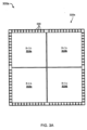
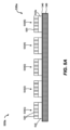
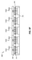
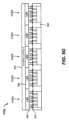
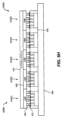
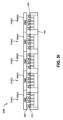
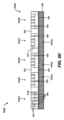
方法800aの一態様において、タイルのアレイは、可撓性基板上に配置される。
Claims (20)
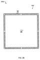
- ディスプレイを制御するためのバックプレーンであって、前記バックプレーンは、
前記バックプレーンの周囲上にある電気コネクタと、
前記バックプレーン上においてタイルアレイに形成された複数のタイルとを備え、前記複数のタイルは、前記タイルアレイの周囲上にあるとともに前記電気コネクタに接続されているタイルを含み、
前記タイル上においてダイアレイに配置されている複数のバックプレーンダイを備え、前記複数のバックプレーンダイは、
前記ダイアレイの周囲上にある縁部を有する第1バックプレーンダイと、
前記第1バックプレーンダイに隣り合っており、かつ、前記ダイアレイの前記周囲上に縁部を有しない第2バックプレーンダイとを含み、前記第2バックプレーンダイは、前記第1バックプレーンダイを経由して前記電気コネクタに接続されている、バックプレーン。 - 前記複数のバックプレーンダイのうちのバックプレーンダイは、前記ディスプレイの発光素子を駆動するための電気信号を生成する相補型金属酸化膜半導体(CMOS)集積回路を含む、請求項1に記載のバックプレーン。
- 前記複数のバックプレーンダイのうちのバックプレーンダイは、前記ディスプレイの光反射素子への電気信号を生成するための相補型金属酸化膜半導体(CMOS)集積回路を含む、請求項1に記載のバックプレーン。
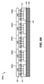
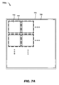
- 前記複数のタイルが2×2タイルアレイとして形成されている場合、各タイルは2つの縁部を有し、各縁部は前記タイルアレイの前記周囲に位置する電気接続を有する、請求項1から請求項3のいずれか一項に記載のバックプレーン。
- 前記複数のバックプレーンダイのうちの前記第1バックプレーンダイは、前記タイル上の前記ダイアレイにおけるの残りのバックプレーンダイへの外部電気接続を提供する、請求項1から請求項4のいずれか一項に記載のバックプレーン。
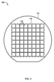
- 前記複数のバックプレーンダイは、長方形または正方形のダイアレイに配置され、
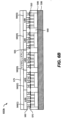
前記複数のバックプレーンダイのうちのバックプレーンダイは、電気再分配層(RDL)を介して、前記ディスプレイのLEDアレイに電気的に接続された複数のピラーを含む、請求項1に記載のバックプレーン。 - 前記タイルは、前記複数のバックプレーンダイ間のギャップを充填し、かつ、前記複数のバックプレーンダイを共に保持するように構成されているオーバーモールドを含む、請求項1から請求項6のいずれか一項に記載のバックプレーン。
- 前記オーバーモールドは、シリカ材料、アルミナ材料、グラファイト材料、セラミック材料、またはポリマー材料の少なくとも一つから形成される、請求項7に記載のバックプレーン。
- 前記タイルは、前記複数のバックプレーンダイを確実に支持するための基板を含む、請求項1から請求項8のいずれか一項に記載のバックプレーン。
- 前記基板は、剛性であり、かつ、前記複数のバックプレーンダイのうちの少なくとも1つへの電気接続を提供する複数のシリコン貫通ビア(TSV)を含む、請求項9に記載のバックプレーン。
- バックプレーンを備え、前記バックプレーンは、
前記バックプレーンの周囲上にある電気コネクタと、
タイルのアレイとを含み、前記タイルのアレイは、前記タイルのアレイの周囲上にあるとともに前記電気コネクタに接続されているタイルを含み、
前記タイル上においてダイアレイに配置されている、電気的に結合された複数のバックプレーンダイを含み、前記複数のバックプレーンダイは、
前記ダイアレイの周囲上にある縁部を有する第1バックプレーンダイと、
前記第1バックプレーンダイに隣り合っており、かつ、前記ダイアレイの前記周囲上に縁部を有しない第2バックプレーンダイとを含み、前記第2バックプレーンダイは、前記第1バックプレーンダイを経由して前記電気コネクタに接続されており、
前記タイルに電気的に結合された発光ダイオード(LED)アレイを備える、ディスプレイアセンブリ。 - 前記タイルは、前記第1バックプレーンダイまたは前記第2バックプレーンダイの少なくとも1つのピラーを前記LEDアレイに電気的に接続するために、前記第1バックプレーンダイ及び前記第2バックプレーンダイの各々の少なくとも一部に配置された電気再分配層を含む、請求項11に記載のディスプレイアセンブリ。
- 前記LEDアレイからの光を屈折させるように構成された少なくとも1つのマイクロレンズアレイをさらに備える、請求項11または請求項12に記載のディスプレイアセンブリ。
- 前記少なくとも1つのマイクロレンズアレイは、前記タイルのアレイを覆う単一のマイクロレンズアレイを含む、請求項13に記載のディスプレイアセンブリ。
- 前記少なくとも1つのマイクロレンズアレイは、複数のマイクロレンズアレイを含み、
前記複数のマイクロレンズアレイの各々は、前記タイルのアレイの異なるタイルを覆う、請求項13に記載のディスプレイアセンブリ。 - 前記少なくとも1つのマイクロレンズアレイは、複数のマイクロレンズアレイを含み、
前記複数のマイクロレンズアレイの各々は、前記複数のバックプレーンダイのうちの単一のバックプレーンダイを覆う、請求項13に記載のディスプレイアセンブリ。 - 前記タイルは、前記複数のバックプレーンダイを強固に支持する基板を含む、請求項11から請求項16のいずれか一項に記載のディスプレイアセンブリ。
- 前記基板は、前記複数のバックプレーンダイのうちの少なくとも1つへの電気接続を提供する複数のシリコン貫通ビア(TSV)をさらに含む、請求項17に記載のディスプレイアセンブリ。
- 前記タイルは、前記複数のバックプレーンダイ間のギャップを充填し、かつ、前記複数のバックプレーンダイを強固に支持するように構成されたオーバーモールドを含む、請求項11から請求項18のいずれか一項に記載のディスプレイアセンブリ。
- 前記オーバーモールドは、シリカ材料、アルミナ材料、グラファイト材料、セラミック材料、またはポリマー材料の少なくとも一つから形成される、請求項19に記載のディスプレイアセンブリ。
Applications Claiming Priority (3)
| Application Number | Priority Date | Filing Date | Title |
|---|---|---|---|
| US202063005731P | 2020-04-06 | 2020-04-06 | |
| US63/005,731 | 2020-04-06 | ||
| PCT/US2021/025881 WO2021207129A1 (en) | 2020-04-06 | 2021-04-06 | Display assemblies |
Publications (2)
| Publication Number | Publication Date |
|---|---|
| JP2023522583A JP2023522583A (ja) | 2023-05-31 |
| JP7581367B2 true JP7581367B2 (ja) | 2024-11-12 |
Family
ID=77922191
Family Applications (1)
| Application Number | Title | Priority Date | Filing Date |
|---|---|---|---|
| JP2022560993A Active JP7581367B2 (ja) | 2020-04-06 | 2021-04-06 | バックプレーン及びディスプレイアセンブリ |
Country Status (7)
| Country | Link |
|---|---|
| US (1) | US12107072B2 (ja) |
| EP (1) | EP4133475A4 (ja) |
| JP (1) | JP7581367B2 (ja) |
| KR (1) | KR102785804B1 (ja) |
| CN (1) | CN115362491B (ja) |
| TW (1) | TWI891764B (ja) |
| WO (1) | WO2021207129A1 (ja) |
Families Citing this family (10)
| Publication number | Priority date | Publication date | Assignee | Title |
|---|---|---|---|---|
| US11862585B2 (en) * | 2020-02-21 | 2024-01-02 | Advanced Semiconductor Engineering, Inc. | Semiconductor package structures and methods of manufacturing the same |
| JP7510820B2 (ja) * | 2020-08-31 | 2024-07-04 | シャープ福山レーザー株式会社 | 画像表示素子 |
| WO2022147030A1 (en) * | 2020-12-29 | 2022-07-07 | Raxium, Inc. | Extended depth range light field display |
| JP7317176B1 (ja) | 2022-04-26 | 2023-07-28 | 株式会社アドバンテスト | 試験方法および製造方法 |
| JP7281579B1 (ja) | 2022-04-26 | 2023-05-25 | 株式会社アドバンテスト | 試験方法、製造方法、パネルレベルパッケージおよび試験装置 |
| US20240097087A1 (en) * | 2022-09-16 | 2024-03-21 | Apple Inc. | Method of Transferring Patterned Micro-LED Die onto a Silicon Carrier for Wafer-to-Wafer Hybrid Bonding to a CMOS Backplane |
| US20260107622A1 (en) * | 2022-10-04 | 2026-04-16 | Polymer Forge, Inc. | Microled array with paired through-substrate vias for in-situ polymer synthesis |
| TWI852676B (zh) * | 2023-07-12 | 2024-08-11 | 梭特科技股份有限公司 | Led晶粒混合方法 |
| CN117334711A (zh) * | 2023-07-26 | 2024-01-02 | 上海显耀显示科技有限公司 | Micro led显示面板及制造方法 |
| CN119419204A (zh) * | 2024-09-27 | 2025-02-11 | 佛山市国星电子制造有限公司 | 一种内置驱动芯片的led器件及其制备方法 |
Citations (5)
| Publication number | Priority date | Publication date | Assignee | Title |
|---|---|---|---|---|
| US20020001051A1 (en) | 1999-02-15 | 2002-01-03 | J. Peter Krusius | Method for assembling a tiled, flat- panel microdisplay array |
| JP2018185515A (ja) | 2017-04-25 | 2018-11-22 | ルーメンス カンパニー リミテッド | マイクロledディスプレイ装置 |
| US20190096864A1 (en) | 2015-09-24 | 2019-03-28 | Apple Inc. | Display with embedded pixel driver chips |
| WO2019124952A1 (en) | 2017-12-20 | 2019-06-27 | Seoul Viosys Co., Ltd. | Led unit for display and display apparatus having the same |
| WO2019155243A1 (en) | 2018-02-06 | 2019-08-15 | Holografika Kft | 3d light field led-wall display |
Family Cites Families (166)
| Publication number | Priority date | Publication date | Assignee | Title |
|---|---|---|---|---|
| GB340116A (en) | 1929-12-07 | 1930-12-24 | William Prince Smith | Improvements in and relating to means for facilitating doffing in spinning and analogous machines |
| US2403731A (en) | 1943-04-01 | 1946-07-09 | Eastman Kodak Co | Beam splitter |
| US3936817A (en) | 1974-06-06 | 1976-02-03 | Sidney Levy | Thermoelectric display device |
| DE3176454D1 (en) | 1980-02-22 | 1987-10-22 | Toshiba Kk | Liquid crystal display device |
| US4923285A (en) | 1985-04-22 | 1990-05-08 | Canon Kabushiki Kaisha | Drive apparatus having a temperature detector |
| US5189406A (en) | 1986-09-20 | 1993-02-23 | Thorn Emi Plc | Display device |
| JPH079560B2 (ja) | 1988-07-08 | 1995-02-01 | 工業技術院長 | マッチドフィルタリング方法 |
| EP0358486B1 (en) | 1988-09-07 | 1994-12-28 | Seiko Epson Corporation | Method of driving a liquid crystal display |
| US4996523A (en) | 1988-10-20 | 1991-02-26 | Eastman Kodak Company | Electroluminescent storage display with improved intensity driver circuits |
| DE69022891T2 (de) | 1989-06-15 | 1996-05-15 | Matsushita Electric Ind Co Ltd | Gerät zur Kompensierung von Videosignalen. |
| TW227005B (ja) | 1990-11-14 | 1994-07-21 | Hoechst Ag | |
| JP2932686B2 (ja) | 1990-11-28 | 1999-08-09 | 日本電気株式会社 | プラズマディスプレイパネルの駆動方法 |
| US5144418A (en) | 1990-12-18 | 1992-09-01 | General Electric Company | Crystal stabilization of amplitude of light valve horizontal sweep |
| NL9002808A (nl) | 1990-12-19 | 1992-07-16 | Philips Nv | Inrichting ten behoeve van projectieweergave. |
| US5548347A (en) | 1990-12-27 | 1996-08-20 | Philips Electronics North America Corporation | Single panel color projection video display having improved scanning |
| JP2829149B2 (ja) | 1991-04-10 | 1998-11-25 | シャープ株式会社 | 液晶表示装置 |
| JP3230755B2 (ja) | 1991-11-01 | 2001-11-19 | 富士写真フイルム株式会社 | 平面型表示デバイスのマトリックス駆動方法 |
| US5473338A (en) | 1993-06-16 | 1995-12-05 | In Focus Systems, Inc. | Addressing method and system having minimal crosstalk effects |
| ATE261168T1 (de) | 1992-10-15 | 2004-03-15 | Texas Instruments Inc | Anzeigevorrichtung |
| US5471225A (en) | 1993-04-28 | 1995-11-28 | Dell Usa, L.P. | Liquid crystal display with integrated frame buffer |
| JP3102666B2 (ja) | 1993-06-28 | 2000-10-23 | シャープ株式会社 | 画像表示装置 |
| US5537128A (en) | 1993-08-04 | 1996-07-16 | Cirrus Logic, Inc. | Shared memory for split-panel LCD display systems |
| JP2639311B2 (ja) | 1993-08-09 | 1997-08-13 | 日本電気株式会社 | プラズマディスプレイパネルの駆動方法 |
| CA2137723C (en) | 1993-12-14 | 1996-11-26 | Canon Kabushiki Kaisha | Display apparatus |
| JP3476241B2 (ja) | 1994-02-25 | 2003-12-10 | 株式会社半導体エネルギー研究所 | アクティブマトリクス型表示装置の表示方法 |
| GB9407116D0 (en) | 1994-04-11 | 1994-06-01 | Secr Defence | Ferroelectric liquid crystal display with greyscale |
| US5936604A (en) | 1994-04-21 | 1999-08-10 | Casio Computer Co., Ltd. | Color liquid crystal display apparatus and method for driving the same |
| US5497172A (en) | 1994-06-13 | 1996-03-05 | Texas Instruments Incorporated | Pulse width modulation for spatial light modulator with split reset addressing |
| US5619228A (en) | 1994-07-25 | 1997-04-08 | Texas Instruments Incorporated | Method for reducing temporal artifacts in digital video systems |
| US5757348A (en) | 1994-12-22 | 1998-05-26 | Displaytech, Inc. | Active matrix liquid crystal image generator with hybrid writing scheme |
| JPH08234703A (ja) | 1995-02-28 | 1996-09-13 | Sony Corp | 表示装置 |
| US5751264A (en) | 1995-06-27 | 1998-05-12 | Philips Electronics North America Corporation | Distributed duty-cycle operation of digital light-modulators |
| US5959598A (en) | 1995-07-20 | 1999-09-28 | The Regents Of The University Of Colorado | Pixel buffer circuits for implementing improved methods of displaying grey-scale or color images |
| US6201521B1 (en) | 1995-09-29 | 2001-03-13 | Texas Instruments Incorporated | Divided reset for addressing spatial light modulator |
| JP3834086B2 (ja) | 1995-11-06 | 2006-10-18 | シャープ株式会社 | マトリックス型表示装置およびその駆動方法 |
| US5945972A (en) | 1995-11-30 | 1999-08-31 | Kabushiki Kaisha Toshiba | Display device |
| US5936603A (en) | 1996-01-29 | 1999-08-10 | Delco Electronics Corporation | Liquid crystal display with temperature compensated voltage |
| US5731802A (en) | 1996-04-22 | 1998-03-24 | Silicon Light Machines | Time-interleaved bit-plane, pulse-width-modulation digital display system |
| GB9618593D0 (en) * | 1996-09-06 | 1996-10-16 | Central Research Lab Ltd | Apparatus for displaying an image |
| US6127991A (en) | 1996-11-12 | 2000-10-03 | Sanyo Electric Co., Ltd. | Method of driving flat panel display apparatus for multi-gradation display |
| JPH10164750A (ja) | 1996-11-26 | 1998-06-19 | Nec Corp | 出力電圧可変方式 |
| US6046716A (en) | 1996-12-19 | 2000-04-04 | Colorado Microdisplay, Inc. | Display system having electrode modulation to alter a state of an electro-optic layer |
| US5926162A (en) | 1996-12-31 | 1999-07-20 | Honeywell, Inc. | Common electrode voltage driving circuit for a liquid crystal display |
| US6020687A (en) | 1997-03-18 | 2000-02-01 | Fujitsu Limited | Method for driving a plasma display panel |
| US6369782B2 (en) | 1997-04-26 | 2002-04-09 | Pioneer Electric Corporation | Method for driving a plasma display panel |
| JP3750889B2 (ja) | 1997-07-02 | 2006-03-01 | パイオニア株式会社 | ディスプレイパネルの中間調表示方法 |
| GB2327798B (en) | 1997-07-23 | 2001-08-29 | Sharp Kk | Display device using time division grey scale display method |
| US6518945B1 (en) | 1997-07-25 | 2003-02-11 | Aurora Systems, Inc. | Replacing defective circuit elements by column and row shifting in a flat-panel display |
| US6144356A (en) | 1997-11-14 | 2000-11-07 | Aurora Systems, Inc. | System and method for data planarization |
| JP3279238B2 (ja) | 1997-12-01 | 2002-04-30 | 株式会社日立製作所 | 液晶表示装置 |
| US6034659A (en) | 1998-02-02 | 2000-03-07 | Wald; Steven F. | Active matrix electroluminescent grey scale display |
| US6151011A (en) | 1998-02-27 | 2000-11-21 | Aurora Systems, Inc. | System and method for using compound data words to reduce the data phase difference between adjacent pixel electrodes |
| WO1999057706A2 (en) | 1998-05-04 | 1999-11-11 | Koninklijke Philips Electronics N.V. | Display device |
| US6005558A (en) | 1998-05-08 | 1999-12-21 | Aurora Systems, Inc. | Display with multiplexed pixels for achieving modulation between saturation and threshold voltages |
| US6285360B1 (en) | 1998-05-08 | 2001-09-04 | Aurora Systems, Inc. | Redundant row decoder |
| US6121948A (en) | 1998-05-08 | 2000-09-19 | Aurora Systems, Inc. | System and method for reducing inter-pixel distortion by dynamic redefinition of display segment boundaries |
| US6067065A (en) | 1998-05-08 | 2000-05-23 | Aurora Systems, Inc. | Method for modulating a multiplexed pixel display |
| DE69834821D1 (de) | 1998-07-10 | 2006-07-20 | Orion Electric Co Ltd | Ansteuerungsverfahren für eine wechselstromplasmaanzeigetafel mit erzeugung von grautonstufen |
| US6005649A (en) * | 1998-07-22 | 1999-12-21 | Rainbow Displays, Inc. | Tiled, flat-panel microdisplay array having visually imperceptible seams |
| JP2994632B1 (ja) | 1998-09-25 | 1999-12-27 | 松下電器産業株式会社 | 発光中心変動防止のためのpdp表示の駆動パルス制御装置 |
| US6262703B1 (en) | 1998-11-18 | 2001-07-17 | Agilent Technologies, Inc. | Pixel cell with integrated DC balance circuit |
| GB9827964D0 (en) | 1998-12-19 | 1999-02-10 | Secr Defence | Active backplane circuitry |
| GB9827944D0 (en) | 1998-12-19 | 1999-02-10 | Secr Defence | Displays based on multiple digital bit planes |
| KR100375806B1 (ko) | 1999-02-01 | 2003-03-15 | 가부시끼가이샤 도시바 | 색 얼룩 보정 장치 및 휘도 얼룩 보정 장치 |
| US6567138B1 (en) | 1999-02-15 | 2003-05-20 | Rainbow Displays, Inc. | Method for assembling a tiled, flat-panel microdisplay array having imperceptible seams |
| JP2000322024A (ja) | 1999-05-11 | 2000-11-24 | Nec Corp | プラズマディスプレイ駆動方法及び駆動装置 |
| AU4844900A (en) | 1999-05-14 | 2000-12-05 | Colorlink, Inc. | Optical system for producing a modulated color image |
| US6642915B1 (en) | 1999-07-13 | 2003-11-04 | Intel Corporation | Display panel |
| US7379039B2 (en) | 1999-07-14 | 2008-05-27 | Sony Corporation | Current drive circuit and display device using same pixel circuit, and drive method |
| JP3665515B2 (ja) | 1999-08-26 | 2005-06-29 | セイコーエプソン株式会社 | 画像表示装置 |
| JP3433406B2 (ja) | 1999-10-18 | 2003-08-04 | インターナショナル・ビジネス・マシーンズ・コーポレーション | ホワイトポイント調整方法、カラー画像処理方法、ホワイトポイント調整装置、および液晶表示装置 |
| US6771325B1 (en) | 1999-11-05 | 2004-08-03 | Texas Instruments Incorporated | Color recapture for display systems |
| JP3606138B2 (ja) | 1999-11-05 | 2005-01-05 | セイコーエプソン株式会社 | ドライバic、電気光学装置及び電子機器 |
| JP3840856B2 (ja) | 1999-11-10 | 2006-11-01 | セイコーエプソン株式会社 | 液晶パネルの駆動方法、液晶装置および電子機器 |
| EP1113412B1 (en) | 1999-12-27 | 2014-05-21 | Japan Display Inc. | Liquid crystal display apparatus and method for driving the same |
| KR100758622B1 (ko) | 2000-01-14 | 2007-09-13 | 마쯔시다덴기산교 가부시키가이샤 | 액티브 매트릭스형 표시장치 및 그 구동방법 |
| WO2001056004A1 (en) | 2000-01-31 | 2001-08-02 | Three-Five Systems, Inc. | Methods and apparatus for driving a display |
| JP3558959B2 (ja) | 2000-05-25 | 2004-08-25 | シャープ株式会社 | 温度検出回路およびそれを用いる液晶駆動装置 |
| JP3769463B2 (ja) | 2000-07-06 | 2006-04-26 | 株式会社日立製作所 | 表示装置、表示装置を備えた画像再生装置及びその駆動方法 |
| EP2273778A1 (en) | 2000-07-28 | 2011-01-12 | Melexis Tessenderlo NV | Precise MOS imager transfer function control for expanded dynamic range imaging |
| JP3664059B2 (ja) | 2000-09-06 | 2005-06-22 | セイコーエプソン株式会社 | 電気光学装置の駆動方法、駆動回路及び電気光学装置並びに電子機器 |
| TW482991B (en) | 2000-09-13 | 2002-04-11 | Acer Display Tech Inc | Power-saving driving circuit for plasma display panel |
| GB2367413A (en) | 2000-09-28 | 2002-04-03 | Seiko Epson Corp | Organic electroluminescent display device |
| US7184014B2 (en) | 2000-10-05 | 2007-02-27 | Semiconductor Energy Laboratory Co., Ltd. | Liquid crystal display device |
| JP2002116741A (ja) | 2000-10-10 | 2002-04-19 | Optrex Corp | 液晶表示素子の表示輝度の調整方法および液晶表示装置 |
| JP4552069B2 (ja) | 2001-01-04 | 2010-09-29 | 株式会社日立製作所 | 画像表示装置およびその駆動方法 |
| JP2002215095A (ja) | 2001-01-22 | 2002-07-31 | Pioneer Electronic Corp | 発光ディスプレイの画素駆動回路 |
| JP2002244202A (ja) | 2001-02-14 | 2002-08-30 | Sony Corp | 液晶プロジェクタ装置および液晶プロジェクタ装置の駆動方法 |
| JP4663896B2 (ja) | 2001-03-30 | 2011-04-06 | 株式会社日立製作所 | 液晶表示装置 |
| US6690432B2 (en) | 2001-04-12 | 2004-02-10 | Koninklijke Philips Electronics N.V. | Alignment of the optical and the electrical scan in a scrolling color projector |
| US6744415B2 (en) | 2001-07-25 | 2004-06-01 | Brillian Corporation | System and method for providing voltages for a liquid crystal display |
| US7576734B2 (en) | 2001-10-30 | 2009-08-18 | Semiconductor Energy Laboratory Co., Ltd. | Signal line driving circuit, light emitting device, and method for driving the same |
| FR2832843A1 (fr) | 2001-11-29 | 2003-05-30 | Thomson Licensing Sa | Procede pour ameliorer le rendement lumineux d'un afficheur matriciel a affichage sequentiel des couleurs |
| US6762739B2 (en) | 2002-02-14 | 2004-07-13 | Aurora Systems, Inc. | System and method for reducing the intensity output rise time in a liquid crystal display |
| US9583031B2 (en) | 2002-05-10 | 2017-02-28 | Jasper Display Corp. | Modulation scheme for driving digital display systems |
| US8421828B2 (en) | 2002-05-10 | 2013-04-16 | Jasper Display Corp. | Modulation scheme for driving digital display systems |
| US7129920B2 (en) | 2002-05-17 | 2006-10-31 | Elcos Mircrodisplay Technology, Inc. | Method and apparatus for reducing the visual effects of nonuniformities in display systems |
| US6781737B2 (en) | 2002-08-13 | 2004-08-24 | Thomson Licensing S.A. | Pulse width modulated display with hybrid coding |
| US20050052437A1 (en) | 2002-08-14 | 2005-03-10 | Elcos Microdisplay Technology, Inc. | Temperature sensor circuit for microdisplays |
| US7088329B2 (en) | 2002-08-14 | 2006-08-08 | Elcos Microdisplay Technology, Inc. | Pixel cell voltage control and simplified circuit for prior to frame display data loading |
| US7468717B2 (en) | 2002-12-26 | 2008-12-23 | Elcos Microdisplay Technology, Inc. | Method and device for driving liquid crystal on silicon display systems |
| US7136042B2 (en) | 2002-10-29 | 2006-11-14 | Microsoft Corporation | Display controller permitting connection of multiple displays with a single video cable |
| US6784898B2 (en) | 2002-11-07 | 2004-08-31 | Duke University | Mixed mode grayscale method for display system |
| US6791759B2 (en) * | 2002-12-18 | 2004-09-14 | Intel Corporation | Focus-position compensator |
| US7443374B2 (en) | 2002-12-26 | 2008-10-28 | Elcos Microdisplay Technology, Inc. | Pixel cell design with enhanced voltage control |
| US8040311B2 (en) | 2002-12-26 | 2011-10-18 | Jasper Display Corp. | Simplified pixel cell capable of modulating a full range of brightness |
| TW594634B (en) | 2003-02-21 | 2004-06-21 | Toppoly Optoelectronics Corp | Data driver |
| DE10307525B4 (de) | 2003-02-21 | 2006-03-16 | Litef Gmbh | Verfahren und Einrichtung zur Erhöhung der Auflösung eines digitalen Phasenmodulators für eine faseroptische Signalübertragungs- oder Messeinrichtung |
| JP4846571B2 (ja) | 2003-04-24 | 2011-12-28 | ディスプレイテック,インコーポレイテッド | 微小表示装置システム及び画像を表示する方法 |
| JP3918770B2 (ja) | 2003-04-25 | 2007-05-23 | セイコーエプソン株式会社 | 電気光学装置、電気光学装置の駆動方法および電子機器 |
| JP5122131B2 (ja) | 2003-04-25 | 2013-01-16 | 統寶光電股▲ふん▼有限公司 | アクティブマトリクスディスプレイパネルを駆動する方法および装置 |
| JP3870933B2 (ja) | 2003-06-24 | 2007-01-24 | ソニー株式会社 | 表示装置及びその駆動方法 |
| ITMI20031518A1 (it) | 2003-07-24 | 2005-01-25 | Dora Spa | Metodo di pilotaggio di moduli lcd a basso consumo |
| US20050062765A1 (en) | 2003-09-23 | 2005-03-24 | Elcos Microdisplay Technology, Inc. | Temporally dispersed modulation method |
| US20080007576A1 (en) | 2003-11-01 | 2008-01-10 | Fusao Ishii | Image display device with gray scales controlled by oscillating and positioning states |
| US8228595B2 (en) | 2003-11-01 | 2012-07-24 | Silicon Quest Kabushiki-Kaisha | Sequence and timing control of writing and rewriting pixel memories with substantially lower data rate |
| US8081371B2 (en) | 2003-11-01 | 2011-12-20 | Silicon Quest Kabushiki-Kaisha | Spatial light modulator and display apparatus |
| US7502411B2 (en) | 2004-03-05 | 2009-03-10 | Silicon Image, Inc. | Method and circuit for adaptive equalization of multiple signals in response to a control signal generated from one of the equalized signals |
| KR20050112363A (ko) | 2004-05-25 | 2005-11-30 | 삼성전자주식회사 | 표시 장치 |
| US7397980B2 (en) | 2004-06-14 | 2008-07-08 | Optium Australia Pty Limited | Dual-source optical wavelength processor |
| TWI228744B (en) | 2004-07-12 | 2005-03-01 | Au Optronics Corp | Plasma display panel and method for driving thereof |
| TWI253050B (en) | 2004-07-14 | 2006-04-11 | Au Optronics Corp | Method of multiple-frame scanning for a display |
| US7067853B1 (en) | 2004-08-26 | 2006-06-27 | Jie Yao | Image intensifier using high-sensitivity high-resolution photodetector array |
| US20060066645A1 (en) | 2004-09-24 | 2006-03-30 | Ng Sunny Y | Method and apparatus for providing a pulse width modulation sequence in a liquid crystal display |
| CA2496642A1 (en) | 2005-02-10 | 2006-08-10 | Ignis Innovation Inc. | Fast settling time driving method for organic light-emitting diode (oled) displays based on current programming |
| US7545396B2 (en) | 2005-06-16 | 2009-06-09 | Aurora Systems, Inc. | Asynchronous display driving scheme and display |
| US8339428B2 (en) | 2005-06-16 | 2012-12-25 | Omnivision Technologies, Inc. | Asynchronous display driving scheme and display |
| US8111271B2 (en) | 2006-04-27 | 2012-02-07 | Jasper Display Corporation | Gray scale drive sequences for pulse width modulated displays |
| US7852307B2 (en) | 2006-04-28 | 2010-12-14 | Jasper Display Corp. | Multi-mode pulse width modulated displays |
| US20080158437A1 (en) | 2006-12-27 | 2008-07-03 | Kazuma Arai | Method for displaying digital image data and digital color display apparatus |
| US8643681B2 (en) | 2007-03-02 | 2014-02-04 | Silicon Quest Kabushiki-Kaisha | Color display system |
| US8223179B2 (en) | 2007-07-27 | 2012-07-17 | Omnivision Technologies, Inc. | Display device and driving method based on the number of pixel rows in the display |
| DE102007051520B4 (de) | 2007-10-19 | 2021-01-14 | Seereal Technologies S.A. | Komplexwertiger räumlicher Lichtmodulator, räumliche Lichtmodulationseinrichtung und Verfahren zur Modulation eines Wellenfeldes |
| US8120555B2 (en) | 2007-11-02 | 2012-02-21 | Global Oled Technology Llc | LED display with control circuit |
| DE112008003278T5 (de) | 2007-12-05 | 2011-04-07 | Hamamatsu Photonics K.K., Hamamatsu | Phasenmodulationsvorrichtung und Phasenmodulationsverfahren |
| DE102009002987B4 (de) | 2008-05-16 | 2018-11-08 | Seereal Technologies S.A. | Steuerbare Vorrichtung zur Phasenmodulation |
| US9024964B2 (en) | 2008-06-06 | 2015-05-05 | Omnivision Technologies, Inc. | System and method for dithering video data |
| US8446309B2 (en) | 2009-02-19 | 2013-05-21 | Cmosis Nv | Analog-to-digital conversion in pixel arrays |
| US9047818B1 (en) | 2009-03-23 | 2015-06-02 | Iii-N Technology, Inc. | CMOS IC for micro-emitter based microdisplay |
| WO2011011548A1 (en) | 2009-07-23 | 2011-01-27 | Dolby Laboratories Licensing Corporation | Reduced power displays |
| US8633873B2 (en) | 2009-11-12 | 2014-01-21 | Ignis Innovation Inc. | Stable fast programming scheme for displays |
| US8605015B2 (en) | 2009-12-23 | 2013-12-10 | Syndiant, Inc. | Spatial light modulator with masking-comparators |
| TW201216249A (en) | 2010-10-07 | 2012-04-16 | Jasper Display Corp | Improved pixel circuit and display system comprising same |
| JP5970758B2 (ja) | 2011-08-10 | 2016-08-17 | セイコーエプソン株式会社 | 電気光学装置、電気光学装置の駆動方法および電子機器 |
| US8645878B1 (en) | 2011-08-23 | 2014-02-04 | Suvolta, Inc. | Porting a circuit design from a first semiconductor process to a second semiconductor process |
| US9025111B2 (en) | 2012-04-20 | 2015-05-05 | Google Inc. | Seamless display panel using fiber optic carpet |
| US8963944B2 (en) | 2012-05-15 | 2015-02-24 | Omnivision Technologies, Inc. | Method, apparatus and system to provide video data for buffering |
| US9175957B2 (en) | 2012-09-24 | 2015-11-03 | Alces Technology, Inc. | Grayscale patterns from binary spatial light modulators |
| US9406269B2 (en) | 2013-03-15 | 2016-08-02 | Jasper Display Corp. | System and method for pulse width modulating a scrolling color display |
| US10311773B2 (en) | 2013-07-26 | 2019-06-04 | Darwin Hu | Circuitry for increasing perceived display resolutions from an input image |
| US9589514B2 (en) | 2014-02-21 | 2017-03-07 | Texas Instruments Incorporated | Methods and apparatus for reduced bandwidth pulse width modulation |
| US9918053B2 (en) | 2014-05-14 | 2018-03-13 | Jasper Display Corp. | System and method for pulse-width modulating a phase-only spatial light modulator |
| US20160103263A1 (en) * | 2014-10-13 | 2016-04-14 | Google Inc. | Light transmission device with integration structures |
| US20160203801A1 (en) | 2015-01-08 | 2016-07-14 | Pixtronix, Inc. | Low capacitance display address selector architecture |
| US10079264B2 (en) * | 2015-12-21 | 2018-09-18 | Hong Kong Beida Jade Bird Display Limited | Semiconductor devices with integrated thin-film transistor circuitry |
| KR102617466B1 (ko) | 2016-07-18 | 2023-12-26 | 주식회사 루멘스 | 마이크로 led 어레이 디스플레이 장치 |
| US10566976B2 (en) * | 2016-09-19 | 2020-02-18 | International Business Machines Corporation | Complementary logic circuit and application to thin-film hybrid electronics |
| US10629153B2 (en) | 2017-10-13 | 2020-04-21 | Jasper Display Corp. | Backplane suitable to form part of an emissive pixel array and system and methods of modulating same |
| US11030942B2 (en) | 2017-10-13 | 2021-06-08 | Jasper Display Corporation | Backplane adaptable to drive emissive pixel arrays of differing pitches |
| US10437402B1 (en) | 2018-03-27 | 2019-10-08 | Shaoher Pan | Integrated light-emitting pixel arrays based devices by bonding |
| US11100844B2 (en) * | 2018-04-25 | 2021-08-24 | Raxium, Inc. | Architecture for light emitting elements in a light field display |
| US20190347979A1 (en) | 2018-05-08 | 2019-11-14 | Intel Corporation | Micro light-emitting diode displays and pixel structures |
| US10909926B2 (en) | 2018-05-08 | 2021-02-02 | Apple Inc. | Pixel circuitry and operation for memory-containing electronic display |
| US11024220B2 (en) * | 2018-05-31 | 2021-06-01 | Invensas Corporation | Formation of a light-emitting diode display |
| JP2022552799A (ja) * | 2019-10-10 | 2022-12-20 | コーニング インコーポレイテッド | ラップアラウンド電極を形成するためのシステムおよび方法 |
| CN115380324A (zh) * | 2019-12-20 | 2022-11-22 | 亮锐有限责任公司 | 针对led阵列的故障检测和校正 |
-
2021
- 2021-04-06 JP JP2022560993A patent/JP7581367B2/ja active Active
- 2021-04-06 WO PCT/US2021/025881 patent/WO2021207129A1/en not_active Ceased
- 2021-04-06 EP EP21783762.4A patent/EP4133475A4/en active Pending
- 2021-04-06 CN CN202180027007.0A patent/CN115362491B/zh active Active
- 2021-04-06 TW TW110112326A patent/TWI891764B/zh active
- 2021-04-06 US US17/223,299 patent/US12107072B2/en active Active
- 2021-04-06 KR KR1020227038449A patent/KR102785804B1/ko active Active
Patent Citations (6)
| Publication number | Priority date | Publication date | Assignee | Title |
|---|---|---|---|---|
| US20020001051A1 (en) | 1999-02-15 | 2002-01-03 | J. Peter Krusius | Method for assembling a tiled, flat- panel microdisplay array |
| US20190096864A1 (en) | 2015-09-24 | 2019-03-28 | Apple Inc. | Display with embedded pixel driver chips |
| JP2018185515A (ja) | 2017-04-25 | 2018-11-22 | ルーメンス カンパニー リミテッド | マイクロledディスプレイ装置 |
| WO2019124952A1 (en) | 2017-12-20 | 2019-06-27 | Seoul Viosys Co., Ltd. | Led unit for display and display apparatus having the same |
| WO2019155243A1 (en) | 2018-02-06 | 2019-08-15 | Holografika Kft | 3d light field led-wall display |
| JP2021515263A (ja) | 2018-02-06 | 2021-06-17 | ハーレオジェラフィーカー ケーエフティー. | 3dライトフィールドledウォールディスプレイ |
Also Published As
| Publication number | Publication date |
|---|---|
| EP4133475A1 (en) | 2023-02-15 |
| CN115362491A (zh) | 2022-11-18 |
| TW202205240A (zh) | 2022-02-01 |
| KR102785804B1 (ko) | 2025-03-26 |
| CN115362491B (zh) | 2025-04-08 |
| EP4133475A4 (en) | 2024-04-10 |
| TWI891764B (zh) | 2025-08-01 |
| US20210313298A1 (en) | 2021-10-07 |
| KR20220164026A (ko) | 2022-12-12 |
| JP2023522583A (ja) | 2023-05-31 |
| WO2021207129A1 (en) | 2021-10-14 |
| US12107072B2 (en) | 2024-10-01 |
Similar Documents
| Publication | Publication Date | Title |
|---|---|---|
| JP7581367B2 (ja) | バックプレーン及びディスプレイアセンブリ | |
| JP7473702B2 (ja) | シリコン上のカラーiledディスプレイ | |
| US12453204B2 (en) | Semiconductor package and method of manufacturing the same | |
| CN111684576B (zh) | 具有嵌入式像素驱动器芯片的显示器 | |
| US10790267B2 (en) | Light emitting element for pixel and LED display module | |
| TWI387077B (zh) | 晶粒重新配置之封裝結構及其方法 | |
| US20080224192A1 (en) | Packaging methods for imager devices | |
| US12020630B1 (en) | Stacked structure, display screen, and display apparatus | |
| CN113711120A (zh) | 发光二极管显示面板、具有其的显示装置及制造其的方法 | |
| US20190067038A1 (en) | Thrumold post package with reverse build up hybrid additive structure | |
| US20230420429A1 (en) | Chip-on-wafer-on-board structure using spacer die and methods of forming the same | |
| WO2019239687A1 (ja) | 撮像装置 | |
| CN114026689A (zh) | 减少显示设备中的平面度变化 | |
| US10163848B2 (en) | Semiconductor package | |
| US11545512B2 (en) | Image sensor package with underfill and image sensor module including the same | |
| CN118315512A (zh) | 发光器件的制备方法、发光器件及显示装置 | |
| CN118315513A (zh) | 发光器件的制备方法、发光器件及显示装置 | |
| KR102837106B1 (ko) | Led 구동 소자 및 led 구동 소자의 제조 방법 그리고 led 구동 소자를 이용한 디스플레이 장치 | |
| KR20260043619A (ko) | Led 어레이 패키지 및 그의 제조 방법 | |
| TWI905858B (zh) | 微型發光二極體顯示單元及其製造方法 | |
| US20250174618A1 (en) | Display apparatus and fabrication method of the same | |
| CN118315514A (zh) | 发光器件的制备方法、发光器件及显示装置 | |
| CN115552641A (zh) | 包括有源像素ic的发光器件封装及其封装方法 | |
| TW202608292A (zh) | 微型發光二極體顯示單元及其製造方法 | |
| WO2026030490A1 (en) | Efficient assembly for led displays |
Legal Events
| Date | Code | Title | Description |
|---|---|---|---|
| A521 | Request for written amendment filed |
Free format text: JAPANESE INTERMEDIATE CODE: A523 Effective date: 20230207 |
|
| A621 | Written request for application examination |
Free format text: JAPANESE INTERMEDIATE CODE: A621 Effective date: 20230207 |
|
| A977 | Report on retrieval |
Free format text: JAPANESE INTERMEDIATE CODE: A971007 Effective date: 20231227 |
|
| A131 | Notification of reasons for refusal |
Free format text: JAPANESE INTERMEDIATE CODE: A131 Effective date: 20240130 |
|
| A521 | Request for written amendment filed |
Free format text: JAPANESE INTERMEDIATE CODE: A523 Effective date: 20240430 |
|
| A131 | Notification of reasons for refusal |
Free format text: JAPANESE INTERMEDIATE CODE: A131 Effective date: 20240521 |
|
| TRDD | Decision of grant or rejection written | ||
| A01 | Written decision to grant a patent or to grant a registration (utility model) |
Free format text: JAPANESE INTERMEDIATE CODE: A01 Effective date: 20241001 |
|
| A61 | First payment of annual fees (during grant procedure) |
Free format text: JAPANESE INTERMEDIATE CODE: A61 Effective date: 20241030 |
|
| R150 | Certificate of patent or registration of utility model |
Ref document number: 7581367 Country of ref document: JP Free format text: JAPANESE INTERMEDIATE CODE: R150 |