JP4846571B2 - 微小表示装置システム及び画像を表示する方法 - Google Patents
微小表示装置システム及び画像を表示する方法 Download PDFInfo
- Publication number
- JP4846571B2 JP4846571B2 JP2006513274A JP2006513274A JP4846571B2 JP 4846571 B2 JP4846571 B2 JP 4846571B2 JP 2006513274 A JP2006513274 A JP 2006513274A JP 2006513274 A JP2006513274 A JP 2006513274A JP 4846571 B2 JP4846571 B2 JP 4846571B2
- Authority
- JP
- Japan
- Prior art keywords
- pixel
- microdisplay
- data
- pixels
- display device
- Prior art date
- Legal status (The legal status is an assumption and is not a legal conclusion. Google has not performed a legal analysis and makes no representation as to the accuracy of the status listed.)
- Expired - Fee Related
Links
- 238000000034 method Methods 0.000 title claims description 63
- 239000000872 buffer Substances 0.000 claims description 57
- 239000004065 semiconductor Substances 0.000 claims description 30
- 239000000758 substrate Substances 0.000 claims description 28
- 238000005286 illumination Methods 0.000 claims description 8
- 230000009977 dual effect Effects 0.000 claims description 3
- 210000004027 cell Anatomy 0.000 description 88
- 230000035945 sensitivity Effects 0.000 description 41
- XUIMIQQOPSSXEZ-UHFFFAOYSA-N Silicon Chemical compound [Si] XUIMIQQOPSSXEZ-UHFFFAOYSA-N 0.000 description 40
- 229910052710 silicon Inorganic materials 0.000 description 40
- 239000010703 silicon Substances 0.000 description 40
- 238000010586 diagram Methods 0.000 description 21
- 239000004973 liquid crystal related substance Substances 0.000 description 20
- 230000008569 process Effects 0.000 description 19
- 238000003860 storage Methods 0.000 description 19
- 230000008859 change Effects 0.000 description 18
- 238000005070 sampling Methods 0.000 description 18
- 239000005262 ferroelectric liquid crystals (FLCs) Substances 0.000 description 17
- 230000006870 function Effects 0.000 description 17
- 230000006835 compression Effects 0.000 description 11
- 238000007906 compression Methods 0.000 description 11
- 239000000463 material Substances 0.000 description 11
- 239000003086 colorant Substances 0.000 description 10
- 230000002829 reductive effect Effects 0.000 description 9
- 230000004044 response Effects 0.000 description 9
- 238000006243 chemical reaction Methods 0.000 description 7
- 230000010287 polarization Effects 0.000 description 7
- 238000003491 array Methods 0.000 description 6
- 230000008901 benefit Effects 0.000 description 6
- 238000013461 design Methods 0.000 description 6
- 238000005516 engineering process Methods 0.000 description 6
- 238000012545 processing Methods 0.000 description 6
- 230000009466 transformation Effects 0.000 description 6
- 230000000007 visual effect Effects 0.000 description 6
- 230000009471 action Effects 0.000 description 5
- 230000000694 effects Effects 0.000 description 5
- 239000011521 glass Substances 0.000 description 5
- 238000013459 approach Methods 0.000 description 4
- 238000012937 correction Methods 0.000 description 4
- 230000002950 deficient Effects 0.000 description 4
- 230000007613 environmental effect Effects 0.000 description 4
- 238000012986 modification Methods 0.000 description 4
- 230000004048 modification Effects 0.000 description 4
- 239000004988 Nematic liquid crystal Substances 0.000 description 3
- 230000005540 biological transmission Effects 0.000 description 3
- 238000004891 communication Methods 0.000 description 3
- 238000013500 data storage Methods 0.000 description 3
- 230000007547 defect Effects 0.000 description 3
- 238000009826 distribution Methods 0.000 description 3
- 230000010355 oscillation Effects 0.000 description 3
- 230000009467 reduction Effects 0.000 description 3
- 230000002441 reversible effect Effects 0.000 description 3
- 230000007704 transition Effects 0.000 description 3
- OAICVXFJPJFONN-UHFFFAOYSA-N Phosphorus Chemical compound [P] OAICVXFJPJFONN-UHFFFAOYSA-N 0.000 description 2
- 241000529895 Stercorarius Species 0.000 description 2
- 238000004364 calculation method Methods 0.000 description 2
- 239000003990 capacitor Substances 0.000 description 2
- 230000015556 catabolic process Effects 0.000 description 2
- 230000007423 decrease Effects 0.000 description 2
- 238000011982 device technology Methods 0.000 description 2
- 230000005684 electric field Effects 0.000 description 2
- 230000000670 limiting effect Effects 0.000 description 2
- 239000011159 matrix material Substances 0.000 description 2
- 230000007246 mechanism Effects 0.000 description 2
- 230000003287 optical effect Effects 0.000 description 2
- 229910021420 polycrystalline silicon Inorganic materials 0.000 description 2
- 229920005591 polysilicon Polymers 0.000 description 2
- 238000012360 testing method Methods 0.000 description 2
- 239000000853 adhesive Substances 0.000 description 1
- 230000001070 adhesive effect Effects 0.000 description 1
- 229910021417 amorphous silicon Inorganic materials 0.000 description 1
- 230000015572 biosynthetic process Effects 0.000 description 1
- 230000000903 blocking effect Effects 0.000 description 1
- 210000004556 brain Anatomy 0.000 description 1
- 230000003139 buffering effect Effects 0.000 description 1
- 210000001233 cdp Anatomy 0.000 description 1
- 230000000052 comparative effect Effects 0.000 description 1
- 230000002860 competitive effect Effects 0.000 description 1
- 238000004637 computerized dynamic posturography Methods 0.000 description 1
- 239000004020 conductor Substances 0.000 description 1
- 238000006880 cross-coupling reaction Methods 0.000 description 1
- 238000005520 cutting process Methods 0.000 description 1
- 230000006837 decompression Effects 0.000 description 1
- 230000003247 decreasing effect Effects 0.000 description 1
- 238000006731 degradation reaction Methods 0.000 description 1
- 230000003111 delayed effect Effects 0.000 description 1
- 238000001514 detection method Methods 0.000 description 1
- 238000009792 diffusion process Methods 0.000 description 1
- 238000007599 discharging Methods 0.000 description 1
- 239000012769 display material Substances 0.000 description 1
- 238000007667 floating Methods 0.000 description 1
- 238000003780 insertion Methods 0.000 description 1
- 230000037431 insertion Effects 0.000 description 1
- 238000011835 investigation Methods 0.000 description 1
- 238000002955 isolation Methods 0.000 description 1
- 238000004519 manufacturing process Methods 0.000 description 1
- 238000013507 mapping Methods 0.000 description 1
- 238000005259 measurement Methods 0.000 description 1
- 229910021421 monocrystalline silicon Inorganic materials 0.000 description 1
- 230000008450 motivation Effects 0.000 description 1
- 208000001491 myopia Diseases 0.000 description 1
- 230000007935 neutral effect Effects 0.000 description 1
- 238000005192 partition Methods 0.000 description 1
- 230000008447 perception Effects 0.000 description 1
- 230000002093 peripheral effect Effects 0.000 description 1
- 230000000630 rising effect Effects 0.000 description 1
- 238000000926 separation method Methods 0.000 description 1
- 239000002210 silicon-based material Substances 0.000 description 1
- 238000004513 sizing Methods 0.000 description 1
- 239000007787 solid Substances 0.000 description 1
- 230000003595 spectral effect Effects 0.000 description 1
- 230000001360 synchronised effect Effects 0.000 description 1
- 239000010409 thin film Substances 0.000 description 1
- 238000011144 upstream manufacturing Methods 0.000 description 1
Images


Classifications
-
- G—PHYSICS
- G09—EDUCATION; CRYPTOGRAPHY; DISPLAY; ADVERTISING; SEALS
- G09G—ARRANGEMENTS OR CIRCUITS FOR CONTROL OF INDICATING DEVICES USING STATIC MEANS TO PRESENT VARIABLE INFORMATION
- G09G5/00—Control arrangements or circuits for visual indicators common to cathode-ray tube indicators and other visual indicators
-
- G—PHYSICS
- G02—OPTICS
- G02F—OPTICAL DEVICES OR ARRANGEMENTS FOR THE CONTROL OF LIGHT BY MODIFICATION OF THE OPTICAL PROPERTIES OF THE MEDIA OF THE ELEMENTS INVOLVED THEREIN; NON-LINEAR OPTICS; FREQUENCY-CHANGING OF LIGHT; OPTICAL LOGIC ELEMENTS; OPTICAL ANALOGUE/DIGITAL CONVERTERS
- G02F1/00—Devices or arrangements for the control of the intensity, colour, phase, polarisation or direction of light arriving from an independent light source, e.g. switching, gating or modulating; Non-linear optics
- G02F1/01—Devices or arrangements for the control of the intensity, colour, phase, polarisation or direction of light arriving from an independent light source, e.g. switching, gating or modulating; Non-linear optics for the control of the intensity, phase, polarisation or colour
- G02F1/13—Devices or arrangements for the control of the intensity, colour, phase, polarisation or direction of light arriving from an independent light source, e.g. switching, gating or modulating; Non-linear optics for the control of the intensity, phase, polarisation or colour based on liquid crystals, e.g. single liquid crystal display cells
- G02F1/133—Constructional arrangements; Operation of liquid crystal cells; Circuit arrangements
- G02F1/1333—Constructional arrangements; Manufacturing methods
- G02F1/1335—Structural association of cells with optical devices, e.g. polarisers or reflectors
- G02F1/133553—Reflecting elements
-
- G—PHYSICS
- G09—EDUCATION; CRYPTOGRAPHY; DISPLAY; ADVERTISING; SEALS
- G09G—ARRANGEMENTS OR CIRCUITS FOR CONTROL OF INDICATING DEVICES USING STATIC MEANS TO PRESENT VARIABLE INFORMATION
- G09G3/00—Control arrangements or circuits, of interest only in connection with visual indicators other than cathode-ray tubes
- G09G3/20—Control arrangements or circuits, of interest only in connection with visual indicators other than cathode-ray tubes for presentation of an assembly of a number of characters, e.g. a page, by composing the assembly by combination of individual elements arranged in a matrix no fixed position being assigned to or needed to be assigned to the individual characters or partial characters
- G09G3/2003—Display of colours
-
- G—PHYSICS
- G09—EDUCATION; CRYPTOGRAPHY; DISPLAY; ADVERTISING; SEALS
- G09G—ARRANGEMENTS OR CIRCUITS FOR CONTROL OF INDICATING DEVICES USING STATIC MEANS TO PRESENT VARIABLE INFORMATION
- G09G3/00—Control arrangements or circuits, of interest only in connection with visual indicators other than cathode-ray tubes
- G09G3/20—Control arrangements or circuits, of interest only in connection with visual indicators other than cathode-ray tubes for presentation of an assembly of a number of characters, e.g. a page, by composing the assembly by combination of individual elements arranged in a matrix no fixed position being assigned to or needed to be assigned to the individual characters or partial characters
- G09G3/2007—Display of intermediate tones
- G09G3/2014—Display of intermediate tones by modulation of the duration of a single pulse during which the logic level remains constant
-
- G—PHYSICS
- G09—EDUCATION; CRYPTOGRAPHY; DISPLAY; ADVERTISING; SEALS
- G09G—ARRANGEMENTS OR CIRCUITS FOR CONTROL OF INDICATING DEVICES USING STATIC MEANS TO PRESENT VARIABLE INFORMATION
- G09G3/00—Control arrangements or circuits, of interest only in connection with visual indicators other than cathode-ray tubes
- G09G3/20—Control arrangements or circuits, of interest only in connection with visual indicators other than cathode-ray tubes for presentation of an assembly of a number of characters, e.g. a page, by composing the assembly by combination of individual elements arranged in a matrix no fixed position being assigned to or needed to be assigned to the individual characters or partial characters
- G09G3/2085—Special arrangements for addressing the individual elements of the matrix, other than by driving respective rows and columns in combination
- G09G3/2088—Special arrangements for addressing the individual elements of the matrix, other than by driving respective rows and columns in combination with use of a plurality of processors, each processor controlling a number of individual elements of the matrix
-
- G—PHYSICS
- G09—EDUCATION; CRYPTOGRAPHY; DISPLAY; ADVERTISING; SEALS
- G09G—ARRANGEMENTS OR CIRCUITS FOR CONTROL OF INDICATING DEVICES USING STATIC MEANS TO PRESENT VARIABLE INFORMATION
- G09G3/00—Control arrangements or circuits, of interest only in connection with visual indicators other than cathode-ray tubes
- G09G3/20—Control arrangements or circuits, of interest only in connection with visual indicators other than cathode-ray tubes for presentation of an assembly of a number of characters, e.g. a page, by composing the assembly by combination of individual elements arranged in a matrix no fixed position being assigned to or needed to be assigned to the individual characters or partial characters
- G09G3/34—Control arrangements or circuits, of interest only in connection with visual indicators other than cathode-ray tubes for presentation of an assembly of a number of characters, e.g. a page, by composing the assembly by combination of individual elements arranged in a matrix no fixed position being assigned to or needed to be assigned to the individual characters or partial characters by control of light from an independent source
- G09G3/36—Control arrangements or circuits, of interest only in connection with visual indicators other than cathode-ray tubes for presentation of an assembly of a number of characters, e.g. a page, by composing the assembly by combination of individual elements arranged in a matrix no fixed position being assigned to or needed to be assigned to the individual characters or partial characters by control of light from an independent source using liquid crystals
- G09G3/3611—Control of matrices with row and column drivers
- G09G3/3648—Control of matrices with row and column drivers using an active matrix
- G09G3/3651—Control of matrices with row and column drivers using an active matrix using multistable liquid crystals, e.g. ferroelectric liquid crystals
-
- G—PHYSICS
- G11—INFORMATION STORAGE
- G11C—STATIC STORES
- G11C11/00—Digital stores characterised by the use of particular electric or magnetic storage elements; Storage elements therefor
- G11C11/21—Digital stores characterised by the use of particular electric or magnetic storage elements; Storage elements therefor using electric elements
- G11C11/34—Digital stores characterised by the use of particular electric or magnetic storage elements; Storage elements therefor using electric elements using semiconductor devices
- G11C11/40—Digital stores characterised by the use of particular electric or magnetic storage elements; Storage elements therefor using electric elements using semiconductor devices using transistors
- G11C11/41—Digital stores characterised by the use of particular electric or magnetic storage elements; Storage elements therefor using electric elements using semiconductor devices using transistors forming static cells with positive feedback, i.e. cells not needing refreshing or charge regeneration, e.g. bistable multivibrator or Schmitt trigger
- G11C11/413—Auxiliary circuits, e.g. for addressing, decoding, driving, writing, sensing, timing or power reduction
- G11C11/417—Auxiliary circuits, e.g. for addressing, decoding, driving, writing, sensing, timing or power reduction for memory cells of the field-effect type
-
- G—PHYSICS
- G09—EDUCATION; CRYPTOGRAPHY; DISPLAY; ADVERTISING; SEALS
- G09G—ARRANGEMENTS OR CIRCUITS FOR CONTROL OF INDICATING DEVICES USING STATIC MEANS TO PRESENT VARIABLE INFORMATION
- G09G2300/00—Aspects of the constitution of display devices
- G09G2300/04—Structural and physical details of display devices
- G09G2300/0404—Matrix technologies
- G09G2300/0408—Integration of the drivers onto the display substrate
-
- G—PHYSICS
- G09—EDUCATION; CRYPTOGRAPHY; DISPLAY; ADVERTISING; SEALS
- G09G—ARRANGEMENTS OR CIRCUITS FOR CONTROL OF INDICATING DEVICES USING STATIC MEANS TO PRESENT VARIABLE INFORMATION
- G09G2300/00—Aspects of the constitution of display devices
- G09G2300/04—Structural and physical details of display devices
- G09G2300/0421—Structural details of the set of electrodes
- G09G2300/0426—Layout of electrodes and connections
-
- G—PHYSICS
- G09—EDUCATION; CRYPTOGRAPHY; DISPLAY; ADVERTISING; SEALS
- G09G—ARRANGEMENTS OR CIRCUITS FOR CONTROL OF INDICATING DEVICES USING STATIC MEANS TO PRESENT VARIABLE INFORMATION
- G09G2300/00—Aspects of the constitution of display devices
- G09G2300/08—Active matrix structure, i.e. with use of active elements, inclusive of non-linear two terminal elements, in the pixels together with light emitting or modulating elements
- G09G2300/0809—Several active elements per pixel in active matrix panels
- G09G2300/0842—Several active elements per pixel in active matrix panels forming a memory circuit, e.g. a dynamic memory with one capacitor
- G09G2300/0857—Static memory circuit, e.g. flip-flop
-
- G—PHYSICS
- G09—EDUCATION; CRYPTOGRAPHY; DISPLAY; ADVERTISING; SEALS
- G09G—ARRANGEMENTS OR CIRCUITS FOR CONTROL OF INDICATING DEVICES USING STATIC MEANS TO PRESENT VARIABLE INFORMATION
- G09G2310/00—Command of the display device
- G09G2310/02—Addressing, scanning or driving the display screen or processing steps related thereto
- G09G2310/0202—Addressing of scan or signal lines
- G09G2310/0221—Addressing of scan or signal lines with use of split matrices
-
- G—PHYSICS
- G09—EDUCATION; CRYPTOGRAPHY; DISPLAY; ADVERTISING; SEALS
- G09G—ARRANGEMENTS OR CIRCUITS FOR CONTROL OF INDICATING DEVICES USING STATIC MEANS TO PRESENT VARIABLE INFORMATION
- G09G2310/00—Command of the display device
- G09G2310/02—Addressing, scanning or driving the display screen or processing steps related thereto
- G09G2310/0235—Field-sequential colour display
-
- G—PHYSICS
- G09—EDUCATION; CRYPTOGRAPHY; DISPLAY; ADVERTISING; SEALS
- G09G—ARRANGEMENTS OR CIRCUITS FOR CONTROL OF INDICATING DEVICES USING STATIC MEANS TO PRESENT VARIABLE INFORMATION
- G09G2310/00—Command of the display device
- G09G2310/02—Addressing, scanning or driving the display screen or processing steps related thereto
- G09G2310/0243—Details of the generation of driving signals
- G09G2310/0259—Details of the generation of driving signals with use of an analog or digital ramp generator in the column driver or in the pixel circuit
-
- G—PHYSICS
- G09—EDUCATION; CRYPTOGRAPHY; DISPLAY; ADVERTISING; SEALS
- G09G—ARRANGEMENTS OR CIRCUITS FOR CONTROL OF INDICATING DEVICES USING STATIC MEANS TO PRESENT VARIABLE INFORMATION
- G09G2310/00—Command of the display device
- G09G2310/02—Addressing, scanning or driving the display screen or processing steps related thereto
- G09G2310/0264—Details of driving circuits
- G09G2310/027—Details of drivers for data electrodes, the drivers handling digital grey scale data, e.g. use of D/A converters
-
- G—PHYSICS
- G09—EDUCATION; CRYPTOGRAPHY; DISPLAY; ADVERTISING; SEALS
- G09G—ARRANGEMENTS OR CIRCUITS FOR CONTROL OF INDICATING DEVICES USING STATIC MEANS TO PRESENT VARIABLE INFORMATION
- G09G2310/00—Command of the display device
- G09G2310/02—Addressing, scanning or driving the display screen or processing steps related thereto
- G09G2310/0264—Details of driving circuits
- G09G2310/0275—Details of drivers for data electrodes, other than drivers for liquid crystal, plasma or OLED displays, not related to handling digital grey scale data or to communication of data to the pixels by means of a current
-
- G—PHYSICS
- G09—EDUCATION; CRYPTOGRAPHY; DISPLAY; ADVERTISING; SEALS
- G09G—ARRANGEMENTS OR CIRCUITS FOR CONTROL OF INDICATING DEVICES USING STATIC MEANS TO PRESENT VARIABLE INFORMATION
- G09G2310/00—Command of the display device
- G09G2310/02—Addressing, scanning or driving the display screen or processing steps related thereto
- G09G2310/0264—Details of driving circuits
- G09G2310/0289—Details of voltage level shifters arranged for use in a driving circuit
-
- G—PHYSICS
- G09—EDUCATION; CRYPTOGRAPHY; DISPLAY; ADVERTISING; SEALS
- G09G—ARRANGEMENTS OR CIRCUITS FOR CONTROL OF INDICATING DEVICES USING STATIC MEANS TO PRESENT VARIABLE INFORMATION
- G09G2310/00—Command of the display device
- G09G2310/06—Details of flat display driving waveforms
- G09G2310/061—Details of flat display driving waveforms for resetting or blanking
-
- G—PHYSICS
- G09—EDUCATION; CRYPTOGRAPHY; DISPLAY; ADVERTISING; SEALS
- G09G—ARRANGEMENTS OR CIRCUITS FOR CONTROL OF INDICATING DEVICES USING STATIC MEANS TO PRESENT VARIABLE INFORMATION
- G09G2320/00—Control of display operating conditions
- G09G2320/04—Maintaining the quality of display appearance
- G09G2320/041—Temperature compensation
-
- G—PHYSICS
- G09—EDUCATION; CRYPTOGRAPHY; DISPLAY; ADVERTISING; SEALS
- G09G—ARRANGEMENTS OR CIRCUITS FOR CONTROL OF INDICATING DEVICES USING STATIC MEANS TO PRESENT VARIABLE INFORMATION
- G09G2320/00—Control of display operating conditions
- G09G2320/06—Adjustment of display parameters
- G09G2320/0666—Adjustment of display parameters for control of colour parameters, e.g. colour temperature
-
- G—PHYSICS
- G09—EDUCATION; CRYPTOGRAPHY; DISPLAY; ADVERTISING; SEALS
- G09G—ARRANGEMENTS OR CIRCUITS FOR CONTROL OF INDICATING DEVICES USING STATIC MEANS TO PRESENT VARIABLE INFORMATION
- G09G2330/00—Aspects of power supply; Aspects of display protection and defect management
- G09G2330/02—Details of power systems and of start or stop of display operation
- G09G2330/021—Power management, e.g. power saving
-
- G—PHYSICS
- G09—EDUCATION; CRYPTOGRAPHY; DISPLAY; ADVERTISING; SEALS
- G09G—ARRANGEMENTS OR CIRCUITS FOR CONTROL OF INDICATING DEVICES USING STATIC MEANS TO PRESENT VARIABLE INFORMATION
- G09G2340/00—Aspects of display data processing
- G09G2340/02—Handling of images in compressed format, e.g. JPEG, MPEG
-
- G—PHYSICS
- G09—EDUCATION; CRYPTOGRAPHY; DISPLAY; ADVERTISING; SEALS
- G09G—ARRANGEMENTS OR CIRCUITS FOR CONTROL OF INDICATING DEVICES USING STATIC MEANS TO PRESENT VARIABLE INFORMATION
- G09G2340/00—Aspects of display data processing
- G09G2340/04—Changes in size, position or resolution of an image
- G09G2340/0407—Resolution change, inclusive of the use of different resolutions for different screen areas
-
- G—PHYSICS
- G09—EDUCATION; CRYPTOGRAPHY; DISPLAY; ADVERTISING; SEALS
- G09G—ARRANGEMENTS OR CIRCUITS FOR CONTROL OF INDICATING DEVICES USING STATIC MEANS TO PRESENT VARIABLE INFORMATION
- G09G3/00—Control arrangements or circuits, of interest only in connection with visual indicators other than cathode-ray tubes
- G09G3/20—Control arrangements or circuits, of interest only in connection with visual indicators other than cathode-ray tubes for presentation of an assembly of a number of characters, e.g. a page, by composing the assembly by combination of individual elements arranged in a matrix no fixed position being assigned to or needed to be assigned to the individual characters or partial characters
- G09G3/2007—Display of intermediate tones
- G09G3/2059—Display of intermediate tones using error diffusion
-
- G—PHYSICS
- G09—EDUCATION; CRYPTOGRAPHY; DISPLAY; ADVERTISING; SEALS
- G09G—ARRANGEMENTS OR CIRCUITS FOR CONTROL OF INDICATING DEVICES USING STATIC MEANS TO PRESENT VARIABLE INFORMATION
- G09G3/00—Control arrangements or circuits, of interest only in connection with visual indicators other than cathode-ray tubes
- G09G3/20—Control arrangements or circuits, of interest only in connection with visual indicators other than cathode-ray tubes for presentation of an assembly of a number of characters, e.g. a page, by composing the assembly by combination of individual elements arranged in a matrix no fixed position being assigned to or needed to be assigned to the individual characters or partial characters
- G09G3/34—Control arrangements or circuits, of interest only in connection with visual indicators other than cathode-ray tubes for presentation of an assembly of a number of characters, e.g. a page, by composing the assembly by combination of individual elements arranged in a matrix no fixed position being assigned to or needed to be assigned to the individual characters or partial characters by control of light from an independent source
- G09G3/3406—Control of illumination source
- G09G3/3413—Details of control of colour illumination sources
-
- G—PHYSICS
- G09—EDUCATION; CRYPTOGRAPHY; DISPLAY; ADVERTISING; SEALS
- G09G—ARRANGEMENTS OR CIRCUITS FOR CONTROL OF INDICATING DEVICES USING STATIC MEANS TO PRESENT VARIABLE INFORMATION
- G09G3/00—Control arrangements or circuits, of interest only in connection with visual indicators other than cathode-ray tubes
- G09G3/20—Control arrangements or circuits, of interest only in connection with visual indicators other than cathode-ray tubes for presentation of an assembly of a number of characters, e.g. a page, by composing the assembly by combination of individual elements arranged in a matrix no fixed position being assigned to or needed to be assigned to the individual characters or partial characters
- G09G3/34—Control arrangements or circuits, of interest only in connection with visual indicators other than cathode-ray tubes for presentation of an assembly of a number of characters, e.g. a page, by composing the assembly by combination of individual elements arranged in a matrix no fixed position being assigned to or needed to be assigned to the individual characters or partial characters by control of light from an independent source
- G09G3/36—Control arrangements or circuits, of interest only in connection with visual indicators other than cathode-ray tubes for presentation of an assembly of a number of characters, e.g. a page, by composing the assembly by combination of individual elements arranged in a matrix no fixed position being assigned to or needed to be assigned to the individual characters or partial characters by control of light from an independent source using liquid crystals
- G09G3/3611—Control of matrices with row and column drivers
- G09G3/3685—Details of drivers for data electrodes
- G09G3/3688—Details of drivers for data electrodes suitable for active matrices only
-
- G—PHYSICS
- G09—EDUCATION; CRYPTOGRAPHY; DISPLAY; ADVERTISING; SEALS
- G09G—ARRANGEMENTS OR CIRCUITS FOR CONTROL OF INDICATING DEVICES USING STATIC MEANS TO PRESENT VARIABLE INFORMATION
- G09G5/00—Control arrangements or circuits for visual indicators common to cathode-ray tube indicators and other visual indicators
- G09G5/02—Control arrangements or circuits for visual indicators common to cathode-ray tube indicators and other visual indicators characterised by the way in which colour is displayed
Description
するには、各表示画素が多数の明るさレベルを表示できる必要がある。このことは、アナログ応答画素発光体またはアナログ回路付変調装置を駆動することにより達成できる。アナログ回路に対して特化したシリコン組み立て工程は知られているが、通常、標準デジタル工程より費用がかかる。さらに、アナログ回路の設計は、同様のデジタル回路の設計よりも困難であり、かつ、より大きな手間を必要とする。アナログ回路は、もし慎重に管理されなければ不要な画像擬似信号を生成し得る様々な雑音およびオフセット効果を受けやすい。したがって、純粋なデジタル回路を介して濃度諧調を供給することが望ましい。
に存在するメモリ・セルを含み得る。輝度データは各々の個別画素に対して保存され、色データは複数の画素のグループに対して保存されている。画素の各グループは4つの画素を含み得る。微小表示装置内の画素は複数の行および列に配列可能であり、4つの画素の各グループは特定の行に2つの隣接した画素を、および、隣接した1つの行に2つの隣接した画素を含み、そのため、画素の2つは1つの列にあり、画素の2つは1つの隣接した列にある。
本発明は画像データを表示するための微小表示装置システムにも関し得る。システムは異なった表示状態間で切換え可能な画素のアレイを有する微小表示装置を含み、微小表示装置は半導体基板上に存在し、かつ、デジタル・インタフェイス・デバイスも同じく前記半導体基板上に存在し、インタフェイス・デバイスは第1のフォーマットにおいて画像データを受入れ、かつ、画像データを第2のフォーマットにおいて微小表示装置の画素に供給する。微小表示装置の各画素は画素電極を含み、画素は、画素電圧源が、微小表示装置の選択された画素電極に、残り部分を駆動するために使用される論理電圧源により供給される電圧とは異なった大きさで電圧を供給するために使用されることを可能にするための回路も含む。
装置は半導体基板上に存在し、デジタル・インタフェイス・デバイスも同じく前記半導体基板上に存在し、インタフェイス・デバイスは第1のフォーマットにおいて画像データを受入れ、かつ、画像データを第2のフォーマットにおいて微小表示装置の画素に供給し、不揮発性メモリは微小表示装置に接続され、その特定の微小表示装置システムに固有の情報を保存し、それにより、微小表示装置は保存された情報を利用可能であり、かつ、この情報に基づき、微小表示装置システムにより表示された画像の品質を向上できる。
本発明は画像データを表示するための微小表示装置システムにも関し得る。システムは異なった表示状態間で切換え可能な画素のアレイを有する微小表示装置を含み、微小表示装置は半導体基板上に存在し、デジタル・インタフェイス・デバイスも同じく前記半導体基板上に存在し、インタフェイス・デバイスは第1のフォーマットにおいて画像データを受入れ、かつ、画像データを第2のフォーマットにおいて微小表示装置の画素に供給する。微小表示装置における画素のアレイは行に配列され、行の第1の部分は1つのグループ内にあり、行の第2の部分は第2のグループ内にあり、かつ、さらに、第1および第2のグループの1つのグループの画素は画像情報を使用して頂部行から底部行に更新される一方、第1および第2のグループの別のグループの画素は画像情報を使用して底部行から頂部行に更新される。
本発明は画像データを表示するための微小表示装置システムにも関し得る。システムは異なった光変調状態間で切換え可能な画素のアレイを有する空間光変調装置を含み、空間光変調装置は半導体基板上に存在し、デジタル・インタフェイス・デバイスも同じく前記半導体基板上に存在し、インタフェイス・デバイスは第1のフォーマットにおいて画像データを受入れ、かつ、画像データを第2のフォーマットにおいて空間光変調装置の画素に供給する。空間光変調装置は表示される画像データを保存するためのメモリ・セルを含み、メモリ・セルは空間光変調装置全体を通じて分配され、分配されたメモリ・セルは画素アレイと同位置に存在するが、画素アレイの特定の画素に物理的に接続し得ず、かつ、さらに、各画素は反射性画素電極を含み、反射性画素電極は第1の面内に横たわり、かつ、分配されたメモリ・セルは第1の平面であり、かつ、同平面に平行である第2の面内に横たわり、かつ、さらに、反射性画素電極の少なくともいくつかの第2の平面上への正射影は、別の反射性画素電極に対する画像情報を保存しているメモリ・セルを覆っている。
ット数より小さい各画素に対する数のビットをデータ保存アレイに保存し、それにより、保存された画像を作成する工程と、その画素に対して保存されたビット数より大きいビット数を各画素に対して表示することにより、保存された画像を画素アレイ上に表示する工程とを含む。
ステムへのデジタル・インタフェイス、画像圧縮、低電力SRAM、および、本発明の他の多くの特徴が必要/所望である他の用途にも本発明が適用可能とし得ることを明白に理解されたい。この点において、微小表示装置システムの以下の説明は例示および説明のみの目的に対して提示されている。さらに、説明は、本願明細書に開示された形態に本発明を限定することは意図されていない。その結果、以下の教示、ならびに、関連技術の技能および知識に相当する改変および修正は本発明の範囲内である。本願明細書に説明されている実施形態は、本発明を実施するうえで知られている最良の形態を説明すること、および、他の当業者が、本発明のそのような、または、他の実施形態において、ならびに、特定の応用例または用途により要求される様々な改変を伴って、本発明を利用することを可能にすることをさらに意図されている。
順次カラー微小表示装置システムは、1つのフォーマットにおいてデータを受信し、かつ、異なったフォーマットにおいてデータを微小表示装置に供給するための追加の回路を必要とする。このフォーマット変換はかなりの量のバッファ・メモリ、表示された画像におけるすべての画素に対する赤、緑、および、青のデータのすべてを保存可能な少なくともメモリの実質的な部分を必ず必要とする。動画の場合、図17に示された「ティアリング(tearing)」擬似信号を防止するために、追加のバッファ・メモリが必要である。[MH1]同図は順次カラー表示装置上の画像を示し、表示装置は新しい入来フレームで同時に更新されつつある単一のフレーム・バッファから再表示されている。描かれた物体は(この例では水平に)移動しつつあり、同物体はフレーム毎に自身の位置を変化させている。表示装置の再表示速度が更新速度とは異なる(すなわち、3倍以上速い)ため、再表示と更新は完全には同期し得ず、したがって、現在のフレームおよびその前のフレームに対応する画像データの部分が表示装置の異なった領域に同時に出現することは不可避である。表示された物体の位置の不整合が存在する水平線がこれらの領域を分離している。物体の詳細または質感はこれらの線に沿って「引き裂かれた」ように見える。この擬似信号は非常に鮮明であり、かつ、平均的な閲覧者には不愉快である。この擬似信号を回避することは、画像データを二重バッファすること、すなわち、前のフレームを保存および表示するために1つのバッファ・メモリを使用する一方、第2のバッファ・メモリが入来画像データで更新されることを必要とする。2つのバッファの役割は入来フレーム間で逆転される。
2μmの周辺の範囲にある画素間隔と対照され得る。したがって、デジタル順次カラー・フォーマット変換の平易な実施は、市場で競争の激しいものより10倍を超えて大きな面積を持つ画素をもたらす。与えられた表示解像度に対して、大きな画素サイズは大きな背面ダイ・サイズをもたらし、このことは、このことに対応して、シリコン・ウェハ当たり少数の背面ダイ、および、低い背面ダイ生産高をもたらし、不要に高い背面ダイのコストを合わせて与える。
このことに留意して、ここで本発明が検討可能となる。本発明が採用可能である応用例の1つの実施例は図1に示された如くのカメラ30である。カメラ30はビデオ・カメラ、デジタル静止画カメラ、または、他のタイプのカメラとし得る。カメラ30はユーザが記録したいと所望可能な画像を表す電気信号を作成可能である画像取込みデバイス32を含み得る。電気信号は画像取込みデバイス32からカメラ30の機能を制御する制御装置34に送られる。カメラ30は、ユーザがカメラ30の動作のモードを選択するために使用可能なユーザ制御部36も含む。制御装置34は、メモリ/テープ部38などの保存デバイスに画像を表す電子信号を保存する能力を有する。ビデオ・カメラの場合、同部38は典型的にビデオ・テープとなり得る一方、デジタル静止画カメラの場合、同部38は典型的に何らかのタイプの電子的不揮発性メモリとなり得る。カメラ30は電力分配部42を介してカメラ30の各構成部分に電力を供給する電池40も含む。画像の保存された電子的表現は、レンズ系46または反射式拡大装置を介してユーザにより閲覧され得る微小表示装置44により視覚的画像に変換可能である。このことは、本発明の微小表示装置が利用され得る応用例の1つの実施例である一方、それは、例示のみの性質を持ち、かつ、本発明の範囲をいかなる形においても限定することは意図されていない。
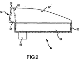
2内に存在するシリコン(LCOS)表示パネル64上の液晶に向けて差向けられる。以下にさらに詳細に説明するように、表示パネルは、2つの異なった光変調状態の1つに電子的に制御可能である画素のアレイを含む。1つの光変調状態において、偏光された入来光は同じ偏光を持ってPBS62に向けて反射し戻される。もう1つの光変調状態において、光は、90度だけ回転された自身の線形偏光を持ってPBS62に向けて反射し戻される。理解され得るように、PBS62は、自身の偏光が回転されなかった反射光を反射する一方、偏光が回転された光は、レンズ系46を介したユーザによる閲覧のためにPBS62を通過する。コネクタ66は屈曲ケーブルを介するなどしたカメラ30への電気的接続のためにパッケージ筐体52から下方に懸垂する。
表示パネル64はさらに詳細に図3および4に示されている。図3に示すように、表示パネル64は、ガラス板72が接着剤封止74を介して固着されているシリコン背面70を含む。シリコン背面70とガラス板72の間に挟まれているのは、液晶材料層76である。異なった側面から見ると、ガラス72および背面70は、1つの側にガラスのわずかな張り出しが、および、向かい合う側にシリコンのわずかな張り出しが存在することを可能にするために、1つの方向においてわずかにずらされていることが明白になり得る。液晶材料76は強誘電性、ネマティック、または、他のタイプの液晶を含むが、これらに限定されないいくつかのタイプの液晶のいずれかを含み得る。この実施形態において、強誘電性液晶が利用されている。代案として、デジタル微小鏡、および、他の微小電子機械デバイス、プラズマ表示装置、エレクトロルミネセント表示装置、発光ダイオードなどの他のタイプの表示デバイスも表示パネルの一部として採用され得る。理解され得るように、これらの代案は、光源からの光を変調する空間光変調装置のいずれかとし得るか、または、独立した光源を必要としない光放射性デバイスとし得る。
実施形態において、これらのメモリ・セルは従来の6トランジスタSRAMとして実施されているが、ダイナミック・レジスタを含む他のタイプのメモリ・レジスタも同様に使用可能である。メモリ・セルの2つの特定の領域、SRAMの第1の領域92およびSRAMの第2の領域94が図5に示されている。見られるように、SRAMの第1の領域92は第1の画素84と機能的に接続され、SRAMの第2の領域94は第2の画素86と機能的に接続されているが、SRAMの領域92および94は第1および第2の画素84および86の隣には所在していない。第2の主要な構成部分は、SRAMセルとしてデータを保存可能であり、ならびに、ブースト・セルに保存されているデータにより指令されたように画素電極に特定の電圧を駆動可能である複数のブースト回路である。
ビット値を表示可能である精度の不足からもたらされるいかなるエラーの目視可能性も最小に抑えるために、制御ブロック116内で実行されるフロイド−スタインバーグ(Floyd−Steinberg)エラー拡散アルゴリズムを使用して8ビット/カラー・データに変換される。加えて、制御ブロック116は、画素アレイのフォーマットに適合する432×240フォーマットへの双線形内挿を使用して(例えば、720×242または720×288のフォーマットを有することがある)入来画像データを水平に、および、垂直に縮尺調整可能である。
続され、かつ、同電極を駆動し、ならびに、ブースト回路144は画素電極152と接続され、かつ、同電極を駆動する。理解され得るように、画素電極146の下方の残りの空間ならびに画素電極148、150、および、152の下方の空間のすべては複数のSRAMメモリ・セル136により占められている。しかし、画素電極132のこの特定のサイズ決定および使用されている特定の半導体組立て工程の場合、特定の画素電極146、148、150、および、152の下方の残りの空間はそれらの4つの画素電極に対するこの設計により必要とされるバッファされた保存に対しては十分ではない。この理由のために、画素アレイ80の垂直に上方および下方の追加の空間は、図5および6に示されたように層130内の追加のSRAM88および90に対して使用されている。
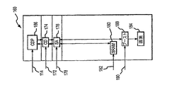
シリコン背面70の各部分は図9に示されている。既に検討されたように、シリコン背面70は分割線100により上部半体および下部半体に分割されている。上部半体は感度増幅器の水平列体102、画素ライン・バッファおよび列駆動装置の水平列体106、ならびに、列データ・プロセッサ(CDP)の水平列体110を含む。さらに、シリコン背面のこの部分は垂直分層に分割され、それらの分層の3つ160、162、および、164が示されていることが観察され得る。各垂直分層は自身のCDPおよび関連画素ライン・バッファ、ならびに、列体106からの列駆動装置ならびに列体102からの関連感度増幅器を有する。特定の分層のCDPはその特定の分層内の画素電極の各々に対するデータ処理を行う。分割線100の別の側には、同様のCDP分層166、168、および、
170が示されている。これらの分層166、168、および、170の各々は単一のCDPおよび関連画素ライン・バッファならびに列体108からの列駆動装置および列体104からの関連感度増幅器を含む。
図10はCDP分層160の機能図を示す。制御部116からの符号化画像データ172は分層160内の列駆動装置174に供給される。列駆動装置174は(この書込み動作に対する信号178を介して選択解除されている)感度増幅器176を通って複数のSRAMメモリ・セル180にデータを送る。データが保存されている特定のSRAMメモリ・セルは列制御部122からの特定の列駆動装置174および行可能信号182により決定される。その後、制御部116は、行制御部122に、画素電極のデータが保存されているSRAMセルの列180に対して行可能信号182を駆動し、かつ、感度増幅器可能信号178を活性化することにより感度増幅器176を可能にするように指令する。感度増幅器176は選択されたSRAMセル180の内容を決定し、かつ、データを分層160のCDP186に送る[JMD2]。CDP186はデータを圧縮解除し、かつ、圧縮解除された値の選択された部分をランプ信号114と比較し、続いて、感度増幅器176を不能にすること、列駆動装置174を可能にすること、および、行制御部122に行可能信号190を駆動させることにより、その比較結果は一時的に保存され、かつ、その後、画素184に接続されたブースト回路188に書き込まれる。
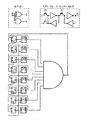
図11は、画素の状態をいつ変化させるかを決定するために、比較を行い、その比較の結果を使用するSRAMからデータを読み出す動作についてさらなる詳細を示す。この場合、SRAMメモリ・セルは、このCDP分層160内の48個の異なったメモリ・セルを含み得るメモリ・セルの行全体として表されている。特定の行180は行可能信号182により選択される。SRAMメモリ180内の特定のメモリ・セルからのデータは感度増幅器176により読み出され、かつ、復号化ブロック200に供給される。このことは以下にさらに詳細に検討する。復号化ブロック200は制御部116から復号化信号202を受信する。復号化信号202は、保存されている符号化された画像データから復号化された結果のどの部分がデジタル比較器204の第1の入力に供給されるべきかを示す。比較器204は符号化された画像値のこの復号化された部分を(その第2の入力に供給された)デジタル・ランプ信号114と比較し、かつ、画素制御信号206を(図12に関連して以下に説明される論理を介して)、画素制御信号206または符号化された画像信号のいずれかの以下の保存場所への書込みを可能にするように制御され得る多重化器208に供給する。この場合、画素制御信号206は、4つの画素184、210、212、および、214の下の列内の4つのブースト回路のグループ内にある選択されたブースト回路188に設けられている(例示の容易さのために、ブースト回路は、この場合、画素の1つの下には示されていない)。ブースト回路188は、画素制御信号206が状態を制御することを意図されている画素電極184に接続され、かつ、電気的に連絡している。この実施形態において、各ブースト回路は画素の所望の状態に対する1ビット保存レジスタとして機能する。8つのブースト回路はブースト回路188を含む行において示されていることが観察され得る。これらは4つのブースト回路の2つのグループにグループ分けされ、4つのブースト回路の下方に示された4つの画素184、210、212、および、214に対する意図された表示値を保存している同回路の最も左のグループ、および、4つのブースト回路の下方に示された4つの画素216、218、220、および、222に対する意図された表示値を保存している同回路の最も左のグループを備えている。後の検討の容易さのために、画素184、210、216、および、218の2×2のアレイが画素グループ224として図11に示されている一方、4つの画素212、214、220、および、222の別のグループが画素グループ226として図11に示されている。
視可能擬似信号を排除するいずれかの他の代案に対するいかなる変形も許容可能である。
本発明の特徴の1つは、制御部116に供給される入来画像データがシリコン背面70
全体を通じて分配されたSRAM画像バッファ内での保存の目的のために圧縮可能であり、かつ、画素による最終的な表示のために圧縮解除可能であることである。圧縮アルゴリズムのいくつかの異なったタイプのいずれもこのことを達成するために利用可能である。1つの手法は、先ず、RGBデータを各画素に対する赤、緑、および、青の値から従来のYUVシステムまたは同システムの変形に変換することである。YUVシステムは輝度成分(Y)および2つの色差信号(UおよびV)を含む。YCBCRで示された1つの共通の版において、色差信号は大部分は赤(CR)および青(CB)の情報を保存し、ここで(緑のほとんども含む)輝度が差し引かれる。以下のマトリクス変換はRGB信号から標準YCBCR信号を生成する。

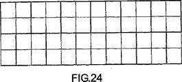
じ頻度で2回サンプリングされ、4:1:1においてはY成分が(図22および23に示されたように、4つの画素を各々が含む太線の長方形により例示されたものと)同じ頻度で4回サンプリングされている。語句4:2:2はしばしば「放送用ビデオ」と呼ばれ、かつ、かなり高品質の画像圧縮フォーマットであると考えられている。最近の民生用デジタル・ビデオ・カムコーダはほとんど専ら4:1:1を使用している。この削減されたサンプリングは画像データの与えられた水平ライン内に通常発生する。したがって、720画素を含む走査線に対しては、図22に示されたように、4:1:1のサンプリング技術は720個の輝度(Y)サンプル、180個のCRサンプル、および、180個のCBサンプルを示唆する。これは4:1:1のNTSC版である。PALシステムは垂直の下位サンプリングも典型的に含む。例えば単一のCRサンプルを共有する4つの水平画素の代わりに、画素の2×2領域は、図23に示されたように、単一のCRサンプルを共有する。このことは、前の走査線を保存するために、ライン・バッファおよびデジタル・ビデオ・システムの追加を必要とするが、この追加はわずかにより満足できる画像を生成する。したがって、4:1:1のPAL版は、サンプリングの幾何学形状のこの差を強調するために、時々4:2:0と示されている。
Di=(1/2)Ri+(1/2)Gi
E=(−1/4)Rave+(−1/4)Gave+(1/2)Bave (3)
F=(1/2)Rave+(−1/2)Gave
となり、逆変換に対しては、
Ri=Di+F
Gi=Di−F (4)
Bi=Di+2E
となる。ここで、下付iは単一の画素に対する値を示す一方、EおよびFは、いくつかの画素にわたり平均されたRave、Gave、および、Baveの値に基づいている。
結果で)満杯となった後、蓄積された値は、単一の書込み動作におけるブースト回路レジスタへの変更の書込みを(特定の比較の結果が等しい場合に)可能にするために、または、(異なった特定の比較の結果が等しくない場合に)可能にしないために使用される。
本発明の微小表示装置は、この装置のフィールド順次カラーの性質により120個の赤
の画像、120個の緑の画像、および、120個の青の画像を意味する毎秒120の完全カラー画像を供給可能である。このことは、同装置が毎秒360個の画像を表示することを根本的に意味し、それは、1秒の360分の1毎または各2.78ミリ秒毎に新しい画像または少なくとも新しいカラー・フィールドを意味する。これらの2.78ミリ秒の間隔の各々の間、符号化されたデータがSRAMメモリ・セルから読み出され、復号化され、かつ、ランプ信号114と255回比較される。したがって、1秒のこれらの360分の1の各々はランプ信号114の255のタイム・スロットに分割される。このことは、秒当たり360×255個のタイム・スロットがあることを意味する。したがって、各タイム・スロットは最大で10.9ミリ秒の長さがある。これらのタイム・スロットの各々の間、新しいデータが各画素の保存レジスタに、このデジタル・パルス幅変調手法で各画素の状態を変更するために書き込まれ得る。
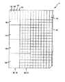
図14はシリコン背面30の層130内のSRAMメモリ・セルのアレイの一部を示す。例示の容易さのために、SRAMメモリ・セルの9つのみが3つの行に示されており、各々は隣接した行内に対応するセルを備えた列内に配列されている。図14のSRAMメモリ・セルは、SRAMメモリ・セルに対する行の数であるXおよび列の数であるYを使用してSRAMXYとラベル付けされている。SRAMメモリ・セルの各列は、同列に接続されたBIT線の対BITYおよびBITYZを有し、ここで、YはBIT線に対する列の数である。SRAMメモリ・セルの各行はワード・ラインWordXを有し、ここで、Xはワード線に対する行の数である。SRAMメモリ・セルの各列に接続されているのは、DIYと示された単一の「データ・イン」回路であり、ここでYは列の数であり、および、SAYと示された感度増幅器であり、ここで、Yは列の数である。データ・イン回路DIYの行は各々がデータ・イン回路の行全体を可能にするために機能するデータ・イン可能信号(DIE)を受信する。各感度増幅器回路(SAY)は感度増幅器の行全体を可能にする増幅器可能信号(SAE)を受信する。データ・インDAYおよび感度増幅器SAYもBITYおよびBITYZ線に接続されている。なぜなら、これが、データがどのようにしてSRAMメモリ・セルに書き込まれ、かつ、これから読み出されるかだからである。各データ・イン回路DIYは選択されたSRAMメモリ・セルに書き込まれるデータを示す分離データ信号DYを受信する。各感度増幅器回路SAYは、選択されたSRAMメモリ・セルから読み出された値を示す感度増幅器出力信号SAOYを供給する。
SRAMメモリ・セルの行全体にデータを書き込むこと、および、同時にSRAMメモリ・セルの行全体からデータを読み出すことは最も典型的である。もし図14に示された第2の行にデータを書き込むことが所望されたとすれば、データDYはDIY回路の各々に供給され、データ・イン可能DIE信号は論理1に設定される。Word2ラインも同じく論理1に設定され、そのため、データDYはデータ・イン回路DIYによりBITYおよびBITYZ線上に置かれる。論理1になっているWord2ラインにより可能となっているSRAMメモリ・セルの第2の行は、以下にさらに説明されるように、BITYおよびBITYZ線にアクセスし、かつ、同線内の値を保存する。続いて、Word2およびDIE信号は論理0に戻され得る。SRAMメモリ・セルの第2の行からデータを読み出すことが所望されると、Word2ラインは論理1に設定され、SRAMメモリ・セルの第2の行SRAM2Yは感度増幅器回路SAYにより読み出されるBITYおよびBITYZ線に関する情報を供給する。一旦、感度増幅器可能信号SAEが論理1に設定されれば、感度増幅器回路SAYは活性化され、BITYおよびBITYZ線に関する情報を読み出し、かつ、SAOY線において出力信号を供給する。
多くの微小表示装置応用例において、微小表示装置により消費される電力を最小に抑えることは重要である。本願明細書において開示されている微小表示装置は、微小表示装置の電力消費量全体へのSRAM動作の寄与を最小に抑えるためのいくつかの特徴を組み込んでおり、この寄与は、そうでなければ、非現実的に大きい。内容を本願明細書に援用するケラー(Khellah)、「A Low−Power High−Performance Current−Mode Multiport SRAM」、IEEE Transactions On VLSI Systems、第9巻第5号、590から598ページ(2001年10月)、ならびに、ブラロック(Blalock)およびジャガー(Jaeger)、「A High−Speed Clamped Bit−Line Current−Mode Sense Amplifier」、IEEE Journal of Solid−State Circuits、第26巻第4号、(1991年4月)に例証されているように、電流モード動作を使用することによりSRAMにより引き出される電力を最小に抑えることを求めることは、メモリ技術において知られている。電流モード動作において、BITYおよびBITYZ線の双方はほぼ不変の電圧レベルに保持され、かつ、両線に(書込み中に)注入される、または、これらから(読出し中に)検出される差分電流はメモリを動作させるために使用される。ビット線の電圧振動Vを小さく保つことにより、ビット線の容量Cを充電および放電することにより引き起こされるCV2の電力放散は小さく保たれる。本微小表示装置の構成においては、多くの読出し動作が各書込み動作に対して発生し、そのため、読出し中の電力消費量は表示装置の電力消費量全体に対して実質的により重要となる。出願人は本微小表示装置の設計中に電流モードの教示を適用しようと試みたが、当技術分野において知られている電流モード感度増幅器が出願人の微小表示装置における使用に十分には適さないことを見出した。従来技術の電流モード感度増幅器はこの微小表示装置SRAMの列間隔により必要とされたきつい間隔で配置することが困難であった。さらに、適切な感度増幅器の感度に対して必要とされたバイアス電流は出願人の微小表示装置のSRAMアレイに対して感度増幅器の大きな電力放散をもたらした。したがって、電流モード動作の使用は本願における本微小表示装置の低電力の目的を凌駕した。
びV2を高くVDDに引き上げる。ビット線も信号PREの制御下でP45およびP46の作用により高くVDDに引き上げる。SRAMの読出しに先立ち、PREは高い状態に移り、ビット線を開放回路に移らせる。次に、Word線は、選択された行のSRAMレジスタをビット線に接続するために高い状態のパルスが送られる。SRAMセルの1つの側は既に高いが、別の側はビット線の1つを低く引き下げ始めている。(ここで示されている実施例におけるBITYZ)。ワード線パルスはビット線の電圧振動を制限するために短く保たれている。典型的な動作において、Word線パルスの幅は4nsとし得、この幅の間、ビット線は200mVのオーダに到達する。次に、感度増幅器は高く上がりつつある信号SAEにより可能とされる。このことは内部ノードV1およびV2を解放し、かつ、N45およびN46を介して電流も流れさせる。(この実施例では200mVのオーダにある)小さな差分電圧がN43とN44のゲート間に出現したとすれば、V1およびV2の内部ノードの1つは他方より速く降下する。N42およびP42のゲートに対してV1の、および、N41およびP41のゲートに対してV2の交差結合により発生されたフィードバックは、ビット線間の小さな電圧差により決定された状態に、感度増幅器を迅速に固定させる。感度増幅器の出力は選択されたSRAMレジスタに本来保存されている状態を明らかにする。
ブースト回路188についてのさらなる詳細は図15a、15b、および、15cに与えられている。ブースト回路は、図15aおよび15bに示されたようにカスコード配列における標準論理低電圧トランジスタから、または、より高電圧のI/Oトランジスタを使用することにより、かつ、図15cに示されたように構築され得る。
図15aに示されたブースト回路の実施形態は保存レジスタ部分260およびブースト部分262を含む。ブースト回路のトランジスタの各々はエンハンスメント・モードのデバイスである。同トランジスタは、ワード線により制御される1対のNチャンネル・アクセス・デバイスN11およびN14を含む。ワード線により論理1にオンとされると、これらのアクセス・デバイスN11およびN14は、保存レジスタ260の残りがそれぞれBITおよびBITZ線に接続されることを可能にする。保存レジスタ260の残りは、1つのインバータがP11およびN12を含み、第2のインバータがP12およびN13を含む1対のインバータを含む。ワード線が論理1に移行されると、BIT線の電圧はN12とP11の間に所在するノード264上に印加される。同様に、N14がオンとされ、BITZ線上の電圧がN13とP12の間のノード266上に印加される。これらのノード264および266の各々が逆のインバータのゲート端末に接続されているため、この状態はアクセス・デバイスN11およびN14がオフとされた後でさえも維持される。
P11およびP12のソース端末はVDDに接続されている。N11、N12、N13、および、N14の各々はアースに接続された自身のPウェル・シリコン基板を有する一方、P11およびP12はVDDに接続された自身のNウェルを有する。
ネルおよびPチャンネル・デバイスに、注意深く制御された対応するバイアス電圧を挿入することにより、同様の方法で制御可能である。温度および他の環境条件などの様々な影響を補償するために、VPIXがこの実施形態においては1.1と1.2ボルトの間の最小値および5ボルトの最大値における電圧から変化可能であることが理解され得る。VPIXが補償のこれらの理由に対して変化されるに従い、VPBIASも変化され、そのため、ブースト回路188内のゲートのいずれにも過剰応力はかけられない。
図15aおよび15bに関して上記に説明されたカスコード・ブースト回路に対する代案として、ブースト回路は、I/Oに対して頻繁に必要とされるより高い電圧レベルで動作するように設計された多くの低電圧CMOS工程において利用可能である如くのトランジスタを使用して実施可能であり、トランジスタは中核論理トランジスタより厚いゲート酸化膜を通常利用している。このようなブースト回路は図15cに示されている。同回路は保存レジスタ部分260およびブースト回路部分304を再び含む。図15cの実施形態において、ブースト部分304は、各々が全電圧VPIXに耐えるように設計された4つのトランジスタN31、N32,P31,および、P32から作成されている。この目的に対して有用なトランジスタは、中核論理VDD値より高い電圧を必要とするI/O機能を実行するために多くの低電圧CMOS工程において供給されるトランジスタを含む。このようなトランジスタは、典型的に、中核論理トランジスタに対して設けられたゲート酸化膜よりも厚いゲート酸化膜を使用して作成される。回路のブースト部分はレジスタ部分260の内部のノード266により再び駆動され、このノード266はレジスタに保存されたビットの値によって電圧ゼロまたはVDDを有する。ノード266が低い状態の時、N31は自身のゲートに印加されたVDDによりオンとされ、N31とP31の間のノードは低い状態に引き下げられ、P32をオンとし、画素電極を高くVPIXに引き上げる。ノード266が高い状態の時、N31はオフとされるが、N32はオンとされ、画素電極を低くアースに引き下げる一方、P32をオフとする。
本発明の微小表示装置44は、動作温度の結果としての微小表示装置44の性能の変化、および、それにより生成された画像への影響を補償するために使用可能である温度補償方式も含む。例えば、微小表示装置に使用されている液晶材料の応答は液晶材料の動作温度により異なり得る。この場合、温度に基づく液晶材料の異なった切換え速度を補償するために、液晶材料に対して異なった駆動電圧を使用することが望ましい。異なった駆動電
圧を選択することにより、液晶の切換え速度を温度変化とは独立にすることが可能となり得る。上記に説明されたように、画素電極に対しては異なる駆動電圧を選択することが可能である。微小表示装置44における温度変化を感知するための回路280が図16に示されている。より詳細には、回路280はシリコン背面70内に所在しても、しなくてもよい。回路280は従来のバンドギャップ参照回路に対する変形とし得る。バンドギャップ参照回路は、第1次に対して温度である電圧を供給し、独立に供給することを意図されている。この場合、回路280は定電流源284により駆動されている並列の8つのダイオードのグループ282を含む。ダイオードのグループ282にかかる定電流源284からの電流により展開された電圧は、増幅器290の正端末への入力として供給される。電圧は、抵抗286および288を含む電圧駆動装置にかかるバンドギャップ電圧によっても展開される。抵抗286にかかる電圧は増幅器290の負端末への入力として供給される。フィードバック抵抗292は増幅器290の利得を決定する。ダイオードのグループ282にかかる電圧は、温度が摂氏20から100度に変化するに従い、約0.7ボルトから0.4ボルトに変化する。増幅器290からの出力は同じ温度範囲に対して1.6ボルトから0.0ボルトに変化する。同図には示されていない増幅器290および従来の下流回路は、電源から所望の電圧源(VPIX)を供給するために、電圧のこの変化を定量化し、電源を制御するために使用されている。この電圧はシリコン背面の動作温度に比例し、温度補償のために使用可能である。温度センサ電圧をデジタル化し、平均温度値を保存されている設定点と比較する制御部116に、この電圧は供給される。温度が、保存された設定点に到達すると、VPIX電圧は、温度の設定点に関連して保存されている電圧値に、多くのフレームにわたり徐々に調整される。画素電極に印加された信号のタイミングも同様に変化し得る。他の環境条件を感知すること、および、駆動信号または照明の電圧またはタイミングを変化させることにより、同条件を補償することが可能である。
上記に説明された微小表示装置の様々な特徴は、以下に説明されるように、電力消費量が低減されて、広範な動作温度範囲にわたり、より優れた表示画面品質を生成する。
望ましい技術で知られているように、順次カラー表示装置において柔軟性を提供するために、および、液晶駆動信号のDCバランスに対処するために、本発明の微小表示装置はビデオ入力データの各フレームに関連したフレーム時間をいくつかの位相、例えば図30に示された如くの12の相に分割する。各位相の間、以下の表に掲げられた変数は独立に制御可能である。
既に説明されたように、一定した照明およびランプ・クロック周波数を持つ単純なPWM方式はγ=1の表示特性を生成する一方、γ=2は限られた濃度ビット深さの知覚的に優れた利用をもたらす。本発明の表示装置は、いくつかの方法で所望のガンマ特性を提供可能である。最初の方法では、LEDの輝度がランプ信号114を使用して一斉に上下する。このことは、画像データ値に対して表示輝度の2次の変化をもたらす。LEDの輝度は、瞬時の電流値に伴うスペクトルの変化を回避するために、好ましくはPWM方式により制御される。
LEDの輝度を変化させるための能力は別の重要な長所を有する。設けられた如くのRGBのLED三連構造体は、様々な色の相対的な明るさのかなりの変化を有し、知覚された白色の変化をもたらす。このことは、参照駆動条件下の様々なLEDの相対輝度を測定すること、および、特定の表示装置のEEPROMに保存可能である効率係数として、これらの測定の結果を提供することにより製造の時点で補正可能である。続いて、動作中に、制御ブロック116の作用下で、様々なLEDに供給された相対駆動強度は、それらの強度の変化を正確に補償するように調整可能であり、一貫した所望の白点をもたらす。
例えば採用され得る強誘電性液晶(FLC)変調装置の特性が所望の温度範囲にわたり劇的に変化してさえも、広い範囲の動作温度にわたり高品質画像を表示する微小表示装置を有することが所望されている。例えば、FLCの切換え速度はFLCの温度が低下されるに従い典型的に低下する。この緩慢な切換えは表示コントラスト比の劣化を引き起こし得る。本発明の微小表示装置はこれらの、および、類似の影響を補償するための方策を提供する。
第1の補償方法は図31に示されているように、LED照明のタイミングの温度変化に関与している。この図は、図30に対して選択された変数の同じ例示的選択肢に対する1つの表示位相の一部を示す。分かり得るように、ランプはブランキング期間の後に開始するが、LED照明の立ち上がりは時間tDだけ遅延されている。本発明の表示装置は、制御ブロック116の作用を介して、温度センサ280により感知された温度に従った遅延持続時間の変化に対処する。例えば、もし表示装置の温度が低下される間、LEDの遅延が一定に保たれたなら、画素FLCの光学的応答の降下するエッジは、同図に示されたように、画素画像値がゼロとなっている時でさえ、かなり遅くなった時点で発生する。このことは、画素により反射される不要な量の光をもたらし、達成可能なコントラスト比を劣化させる。FLC応答のこの遅延は、ランプの開始を基準としたLED照明の遅延を増大させることにより、本発明により補償可能である。予想される様々な温度での所望のLED遅延時間に対する値はEEPROM126[MH5]に保存可能であり、本発明の表示装置と共に使用可能である様々なFLC材料の特性を同表示装置がプログラム可能に補償することをさらに可能にする。
表示装置の様々な特性を補償するための別の方法は、典型的な低温および高温での動作に対する位相の一部の間中に画素にかかる電圧ΔVの波形の例を示す図32を参照して説明されている。低温で、FLCは比較的緩慢に切り換わり、FLCの速度を上昇させるためにより高い駆動電圧が所望される。逆に、高温では、FLCが比較的速く切り換わり、より低い駆動電圧が最適となる。ブースト・セルに関して既に説明されたように、電圧VPIXはVDDより低い電圧からVDDより高い電圧の範囲を通じて変化可能である。同図に示されたように、低温動作に対してはVPIX=4.2Vが選択可能である。同様に、ガラス・ウィンドウ上の共通電極に印加された電圧VWINは変化可能であり、かつ、位相内で様々な値を介して段階的にし得る。図32はブランキング中に0.9Vに設定された電圧VWINおよび2.6Vへの設定を示す。画素電極はブースト・セル・レジスタの状態によって0VまたはVWINに駆動される。結果として得られる液晶にかかる電圧ΔVは、所望の初期状態が迅速に得られることを確実にするために、ブランキングの間、+3.3Vの高い値を有するとして示されている。続いて、濃度スケール変調が発生する位相の一部の間に、画素ΔVは既に得られているオン状態を保持するために+1.6Vに降下される。比較器が、示された画素に対する等しさを検出し、かつ、同画素のブースト・レジスタの状態を変更すると、画素電極電圧は0Vに降下し、変調装置にわたり印加された比較的高いΔV=−2.6Vをもたらす。対照的に、高温では、電圧VPIXはより低い2.0Vに設定され得、VWINは1.0Vに設定され得、一定に保持される。この場合、画素にかかるΔVはブランキングの間に+1.0Vで開始され、その画素のブースト・セル・レジスタが変化されるまで、そのレベルに留まり、そのレベルでΔVは−1.0Vに変化する[MH6]。
さらなる電力節減に対処する少なくとも2つの他のモードがある。先ず、電力は微小表示装置に印加されて保たれ得るが、同装置に送られたいかなる新しい画像データも受信せず、または、いかなる画像も表示し続けないことが可能である。これに続くある時点で、画像の表示を再開するために指令が与えられ得、フレーム・バッファを構成するSRAMメモリ・セルに保存されている画像は、微小表示装置に送信されている新しい画像データがなくても表示可能である。このことは、微小表示装置が内部に所在するデバイスにおける電力節減を、または、通信リンクの受信端に所在している微小表示装置の場合に、そのデバイスに画像データを以前送信していたデバイスにおける電力節減を可能にもたらすことが理解可能であろう。このことは微小表示装置自体による幾分かの電力節減ももたらす。なぜなら、クロックまたはデータの読出しまたは書込みがない一方、画像が表示されなかったからである。第2の電力節減モードは、新しい画像データを受信せずにデータを表示し続ける表示装置を含み得る。このことは、例えば、カメラが、微小表示装置に同じ画像データを送信し続ける必要を無くし得る一方、以前に取り込まれた画像がオペレータによる検討のために表示されているデジタル静止画カメラの応用例に発生し得る。このモードの電力節減は主にカメラにおけるが、微小表示装置はここでも幾分かの電力節減を有する。なぜなら、新しいデータはガンマ補正、縮尺調整、符号化、および、フレーム・バッファへの書込みを有する必要がないからである。
上記に説明された微小表示装置回路および濃度諧調方式は従来技術に対する実質的な長所を有する。画像フィールド当たり限られた数の画素駆動遷移を持つパルス幅変調駆動は完全にデジタルで実施される。JPEGまたは正準4:1:1YUVさえなどのより洗練された圧縮アルゴリズムに必要な回路の複雑さを必要とせずに、「DEF」画像圧縮は画素当たりに保存される必要なビット数を低減する。さらに、PWMを実施するために必要なデジタル比較器は、各画素において実施されるよりも、むしろ多くの画素間で共有される。これらの方法において、表示装置の複雑さは最小に抑えられる。本発明によれば、表
示装置内の画素数が増大されるに従い、画素当たり(だが、画素にではなく)追加される必要のあるトランジスタの数は、144、すなわち、フレーム当たり12ビットの二重バッファ画像保存装置を含む画素当たり24個の6トランジスタSRAMレジスタに、画素ブースト・セルに対する14個のトランジスタを加え、合計158個に等しくなる。DEF方式の代案変形は画素当たりに必要なビット数を12から10にまで低く低減し、画素当たりの複雑さを120+14=134個のトランジスタにさらに低減する。本発明の背景において上記に説明されたように、画像圧縮なしのデジタルPWMアーキテクチャの平易な実施は、もし24ビットの色が所望されれば、画素当たり772個のトランジスタという表示装置の複雑さをもたらす。したがって、本発明による微小表示装置は他の全デジタルPWM実施に比較して実質的に低減された複雑さを有する。より詳細には、本発明は、700未満、600未満、500未満、400未満、300未満、200未満、160未満、150未満、140未満、135未満の限界の追加トランジスタの数値のみを必要とする改善された設計を含む。本発明のより単純な画素はより小さな達成可能な画素サイズに、かつ、したがって、低減されたダイ・サイズ、より高いシリコン利用率、および、低減された背面組立て費用に直接変換される。平易な24ビット・デジタルPWM実施と比較して、本発明の微小表示装置は、各画素に伴う約5倍少ないトランジスタを有し、2.25倍より微細な達成可能な画素間隔をもたらす。
て本発明を利用することを可能にすることをさらに意図されている。添付の特許請求の範囲が、従来技術により許容される程度まで代案実施形態を含むと解釈されることが意図されている。
Claims (16)
- 異なった表示状態間を切換え可能な画素のアレイを有する、半導体基板上に存在する微小表示装置と、
該半導体基板に同じく存在し、第1のフォーマットでデジタル画像データを受信し、かつ、第2のフォーマットで前記微小表示装置の画素に前記デジタル画像データを供給し、前記第1のフォーマットは標準ビデオ信号である、デジタル・インタフェイス・デバイスと、
からなる画像データを表示するための微小表示装置システムであって、
前記第1のフォーマットは、第1の画素に対するRGBデータを含み、次に第2の画素に対するRGBデータが続き、そしてRGB画素データの行全体が供給されるまで順次継続し、その後にRGB画素データの別の行が同様に続き、
前記第2のフォーマットは、第1の色、第2の色、および、第3の色の順次フィールドを含み、
前記微小表示装置は表示される画像データを保存するためのメモリ・セルを備え、同メモリ・セルは前記画素アレイ全体に分散しており、
前記分散したメモリ・セルは、特定の画素と機能的に接続されるが、同特定の画素内に、または、同特定の画素に隣接して必ずしも所在するわけではなく、
前記微小表示装置は、複数の画素を支援する集中型タイミング回路を含み、同集中型タイミング回路は、前記複数の画素の各画素に対してランプ・カウンタ信号と所望の画素値との間で比較を行い、これに基づき、各画素に対する独立した画素状態信号を各画素に送出する、
微小表示装置システム。 - 前記デジタル・インタフェイス・デバイスは、RGBデータを、輝度成分および少なくとも2つの色成分を有するデータ・フォーマットに変換する請求項1に記載の微小表示装置システム。
- 前記微小表示装置は、輝度成分および少なくとも2つの色成分を有する前記データ・フォーマットにおいて前記画像データを保存すべく該微小表示装置内に所在するメモリ・セルを含む請求項2に記載の微小表示装置システム。
- 輝度データは各画素に対して保存され、色データは複数の画素のグループに対して保存される請求項3に記載の微小表示装置システム。
- 前記分配されたメモリ・セルは前記画素アレイとは共存されるが、該画素アレイ内の特定の画素とは物理的に接続されていない請求項1に記載の微小表示装置システム。
- 各画素は反射性画素電極を含み、同反射性画素電極は第1の平面内にあり、かつ、前記分配されたメモリ・セルは該第1の平面に平行な第2の平面内にあり、さらに、該反射性画素電極の少なくともいくつかの該第2の平面上への直角な投影は、別の反射性画素電極に対する画像情報を保存するメモリ・セルを覆う請求項5に記載の微小表示装置システム。
- 照明装置、および、前記半導体基板に装着しているビームスプリッタ・アセンブリをさらに含む請求項1に記載の微小表示装置システム。
- 前記微小表示装置は各画素に対する画像データの2つの連続したフレームを保存するための二連メモリ・バッファを含む請求項1に記載の微小表示装置システム。
- 該微小表示装置は表示される画像データを保存するための、低電力SRAMのメモリ・セルを含む請求項1に記載の微小表示装置システム。
- 該微小表示装置の各画素は画素電極を含み、該画素は、画素電圧源が、該微小表示装置の残り部分を駆動するために使用される論理電圧源により供給される電圧とは異なった大きさの電圧を、選択された画素電極に供給するために使用されることを可能にする回路、を含む請求項1に記載の微小表示装置システム。
- 特定の微小表示装置システムに固有の情報を保存し、それにより、該微小表示装置は該保存された情報を利用可能であり、かつ、該情報に基づき、該微小表示装置システムにより表示される画像の品質を向上する、該微小表示装置に接続された不揮発性メモリ、を含む請求項1に記載の微小表示装置システム。
- 前記微小表示装置における該画素のアレイは行に配列され、該行の第1の部分は1つのグループ内にあり、該行の第2の部分は第2のグループ内にあり、さらに、該第1および該第2のグループの1つのグループの該画素は画像情報を使用して頂部行から底部行に更新される一方、該第1および該第2のグループの別のグループの該画素は画像情報を使用して底部行から頂部行に更新される、請求項1に記載の微小表示装置システム。
- 前記微小表示装置は表示される画像データを保存するためのメモリ・セルを含み、該メモリ・セルは該微小表示装置全体を通じて分配され、該分配されたメモリ・セルは該画素アレイと同位置に存在するが、該画素アレイの特定の画素に物理的には接続されておらず、かつ、さらに、各画素は反射性画素電極を含み、該反射性画素電極は第1の平面内にあり、かつ、該分配されたメモリ・セルは該第1の平面に平行である第2の面内にあり、さらに、該反射性画素電極の少なくともいくつかの該第2の平面上への直角投影は、別の反射性画素電極に対する画像情報を保存しているメモリ・セルを覆っている、請求項1に記載の微小表示装置システム。
- 各画素は内部に回路を有し、該回路は該画素に動作可能に接続され、該画素の内部の、かつ、該画素と動作可能に接続された該回路は複数のトランジスタを含み、該回路中には700未満のトランジスタが存在する請求項1に記載の微小表示装置システム。
- 各画素は表示表面を有し、各画素は該画素の今後の表示状態に関した情報を含む該画素に動作可能に接続された少なくとも1つのメモリ・レジスタを有する微小表示装置と、
各画素および該画素に動作可能に接続された少なくとも1つのメモリ・レジスタにより占められた半導体基板上の表面積は1,000平方ミクロン未満である、請求項1に記載の微小表示装置システム。 - 半導体基板上に存在するデジタル・インタフェイスにおいて、第1のフォーマットでデジタル画像データを受信する工程と、
前記半導体基板上に同じく存在する微小表示装置の画素に対し、第2のフォーマットで前記デジタル画像データを供給する工程と、
前記微小表示装置の画素のアレイにおける一部の画素を、異なった表示状態間で切換える工程と、
を含む、画像を表示する方法であって、
前記第1のフォーマットは、第1の画素に対するRGBデータを含み、次に第2の画素に対するRGBデータが続き、そしてRGB画素データの行全体が供給されるまで順次継続し、その後にRGB画素データの別の行が同様に続き、
前記第2のフォーマットは、第1の色、第2の色、および、第3の色の順次フィールドを含み、
前記微小表示装置は表示される画像データを保存するためのメモリ・セルを備え、同メモリ・セルは前記画素アレイ全体に分散しており、
前記分散したメモリ・セルは、特定の画素と機能的に接続されるが、同特定の画素内に、または、同特定の画素に隣接して必ずしも所在するわけではなく、
前記微小表示装置は、複数の画素を支援する集中型タイミング回路を含み、同集中型タイミング回路は、前記複数の画素の各画素に対してランプ・カウンタ信号と所望の画素値との間で比較を行い、これに基づき、各画素に対する独立した画素状態信号を各画素に送出する、
画像を表示する方法。
Applications Claiming Priority (3)
| Application Number | Priority Date | Filing Date | Title |
|---|---|---|---|
| US46536403P | 2003-04-24 | 2003-04-24 | |
| US60/465,364 | 2003-04-24 | ||
| PCT/US2004/012643 WO2004097506A2 (en) | 2003-04-24 | 2004-04-23 | Microdisplay and interface on a single chip |
Publications (3)
| Publication Number | Publication Date |
|---|---|
| JP2006524844A JP2006524844A (ja) | 2006-11-02 |
| JP2006524844A5 JP2006524844A5 (ja) | 2007-06-14 |
| JP4846571B2 true JP4846571B2 (ja) | 2011-12-28 |
Family
ID=33418231
Family Applications (1)
| Application Number | Title | Priority Date | Filing Date |
|---|---|---|---|
| JP2006513274A Expired - Fee Related JP4846571B2 (ja) | 2003-04-24 | 2004-04-23 | 微小表示装置システム及び画像を表示する方法 |
Country Status (4)
| Country | Link |
|---|---|
| US (7) | US7283105B2 (ja) |
| EP (1) | EP1649445A4 (ja) |
| JP (1) | JP4846571B2 (ja) |
| WO (1) | WO2004097506A2 (ja) |
Families Citing this family (111)
| Publication number | Priority date | Publication date | Assignee | Title |
|---|---|---|---|---|
| US7417782B2 (en) | 2005-02-23 | 2008-08-26 | Pixtronix, Incorporated | Methods and apparatus for spatial light modulation |
| US7283105B2 (en) * | 2003-04-24 | 2007-10-16 | Displaytech, Inc. | Microdisplay and interface on single chip |
| WO2004104790A2 (en) * | 2003-05-20 | 2004-12-02 | Kagutech Ltd. | Digital backplane |
| US7315294B2 (en) * | 2003-08-25 | 2008-01-01 | Texas Instruments Incorporated | Deinterleaving transpose circuits in digital display systems |
| US7916381B2 (en) * | 2003-11-01 | 2011-03-29 | Silicon Quest Kabushiki-Kaisha | Spatial light modulator including drive lines |
| KR100992133B1 (ko) * | 2003-11-26 | 2010-11-04 | 삼성전자주식회사 | 신호 처리 장치 및 방법 |
| US7355612B2 (en) * | 2003-12-31 | 2008-04-08 | Hewlett-Packard Development Company, L.P. | Displaying spatially offset sub-frames with a display device having a set of defective display pixels |
| US7336290B2 (en) | 2004-01-07 | 2008-02-26 | Texas Instruments Incorporated | Method and apparatus for increasing a perceived resolution of a display |
| TW200606492A (en) * | 2004-08-03 | 2006-02-16 | Himax Tech Inc | Displaying method for color-sequential display |
| US7560299B2 (en) * | 2004-08-27 | 2009-07-14 | Idc, Llc | Systems and methods of actuating MEMS display elements |
| TWI331742B (en) * | 2004-09-15 | 2010-10-11 | Ind Tech Res Inst | Brightness control circuit and display device using the same |
| US7602375B2 (en) * | 2004-09-27 | 2009-10-13 | Idc, Llc | Method and system for writing data to MEMS display elements |
| US8514169B2 (en) | 2004-09-27 | 2013-08-20 | Qualcomm Mems Technologies, Inc. | Apparatus and system for writing data to electromechanical display elements |
| US8310441B2 (en) | 2004-09-27 | 2012-11-13 | Qualcomm Mems Technologies, Inc. | Method and system for writing data to MEMS display elements |
| US7150533B2 (en) * | 2004-10-22 | 2006-12-19 | Fakespace Labs, Inc. | LCoS display system with software/firmware correction enabling use of imperfect LCoS chips |
| US9158106B2 (en) | 2005-02-23 | 2015-10-13 | Pixtronix, Inc. | Display methods and apparatus |
| US9082353B2 (en) * | 2010-01-05 | 2015-07-14 | Pixtronix, Inc. | Circuits for controlling display apparatus |
| US7999994B2 (en) | 2005-02-23 | 2011-08-16 | Pixtronix, Inc. | Display apparatus and methods for manufacture thereof |
| US7755582B2 (en) | 2005-02-23 | 2010-07-13 | Pixtronix, Incorporated | Display methods and apparatus |
| US8519945B2 (en) | 2006-01-06 | 2013-08-27 | Pixtronix, Inc. | Circuits for controlling display apparatus |
| US8482496B2 (en) * | 2006-01-06 | 2013-07-09 | Pixtronix, Inc. | Circuits for controlling MEMS display apparatus on a transparent substrate |
| US7746529B2 (en) | 2005-02-23 | 2010-06-29 | Pixtronix, Inc. | MEMS display apparatus |
| US9229222B2 (en) | 2005-02-23 | 2016-01-05 | Pixtronix, Inc. | Alignment methods in fluid-filled MEMS displays |
| US20070205969A1 (en) | 2005-02-23 | 2007-09-06 | Pixtronix, Incorporated | Direct-view MEMS display devices and methods for generating images thereon |
| US8310442B2 (en) | 2005-02-23 | 2012-11-13 | Pixtronix, Inc. | Circuits for controlling display apparatus |
| US9261694B2 (en) | 2005-02-23 | 2016-02-16 | Pixtronix, Inc. | Display apparatus and methods for manufacture thereof |
| US8159428B2 (en) | 2005-02-23 | 2012-04-17 | Pixtronix, Inc. | Display methods and apparatus |
| US8314024B2 (en) * | 2008-12-19 | 2012-11-20 | Unity Semiconductor Corporation | Device fabrication |
| FR2884640A1 (fr) * | 2005-04-15 | 2006-10-20 | Thomson Licensing Sa | Procede d'affichage d'une image video et panneau d'affichage mettant en oeuvre le procede |
| JP2007017615A (ja) * | 2005-07-06 | 2007-01-25 | Sony Corp | 画像処理装置,画像処理方法及びプログラム |
| FR2889763B1 (fr) * | 2005-08-12 | 2007-09-21 | Thales Sa | Afficheur matriciel a affichage sequentiel des couleurs et procede d'adressage |
| US20070097358A1 (en) * | 2005-11-01 | 2007-05-03 | Oon Chin H | System and method for obtaining multi-color optical intensity feedback |
| US20070132705A1 (en) * | 2005-12-12 | 2007-06-14 | Oon Chin H | Display device and method for correlating pixel updates with pixel illumination |
| US8526096B2 (en) | 2006-02-23 | 2013-09-03 | Pixtronix, Inc. | Mechanical light modulators with stressed beams |
| KR101189278B1 (ko) * | 2006-04-18 | 2012-10-09 | 삼성디스플레이 주식회사 | 디지털 아날로그 변환기 및 표시 장치의 구동 방법 |
| EP2541301A3 (en) * | 2006-06-05 | 2013-04-17 | Pixtronix Inc. | Circuits for controlling display apparatus |
| US7876489B2 (en) | 2006-06-05 | 2011-01-25 | Pixtronix, Inc. | Display apparatus with optical cavities |
| JP4320682B2 (ja) * | 2006-07-20 | 2009-08-26 | セイコーエプソン株式会社 | 表示装置、表示装置の駆動方法及び電子機器 |
| US8064118B2 (en) * | 2006-07-27 | 2011-11-22 | Silicon Quest Kabushiki-Kaisha | Control system for micromirror device |
| WO2008026403A1 (fr) * | 2006-08-30 | 2008-03-06 | Nec Corporation | Dispositif de traitement d'image, procédé de traitement d'image, son programme, dispositif d'affichage et système d'affichage d'image |
| US7590015B2 (en) * | 2006-08-30 | 2009-09-15 | Seiko Epson Corporation | Integrated circuit device and electronic instrument |
| WO2008051362A1 (en) | 2006-10-20 | 2008-05-02 | Pixtronix, Inc. | Light guides and backlight systems incorporating light redirectors at varying densities |
| US8228175B1 (en) | 2008-04-07 | 2012-07-24 | Impinj, Inc. | RFID tag chips and tags with alternative behaviors and methods |
| CN101779234A (zh) * | 2007-01-04 | 2010-07-14 | 米克罗恩技术公司 | 数字显示器 |
| CN101221306B (zh) * | 2007-01-12 | 2012-11-21 | 群康科技(深圳)有限公司 | 液晶显示装置及其驱动方法 |
| US7852546B2 (en) | 2007-10-19 | 2010-12-14 | Pixtronix, Inc. | Spacers for maintaining display apparatus alignment |
| US9176318B2 (en) | 2007-05-18 | 2015-11-03 | Pixtronix, Inc. | Methods for manufacturing fluid-filled MEMS displays |
| US8115597B1 (en) * | 2007-03-07 | 2012-02-14 | Impinj, Inc. | RFID tags with synchronous power rectifier |
| US8264482B2 (en) * | 2007-12-19 | 2012-09-11 | Global Oled Technology Llc | Interleaving drive circuit and electro-luminescent display system utilizing a multiplexer |
| US8248560B2 (en) | 2008-04-18 | 2012-08-21 | Pixtronix, Inc. | Light guides and backlight systems incorporating prismatic structures and light redirectors |
| US8326256B1 (en) | 2008-07-15 | 2012-12-04 | Impinj, Inc. | RFID tag with MOS bipolar hybrid rectifier |
| KR101580897B1 (ko) * | 2008-10-07 | 2015-12-30 | 삼성전자주식회사 | 디스플레이 드라이버, 이의 동작 방법, 및 상기 디스플레이 드라이버를 포함하는 장치 |
| US8169679B2 (en) | 2008-10-27 | 2012-05-01 | Pixtronix, Inc. | MEMS anchors |
| US8552957B2 (en) * | 2009-02-02 | 2013-10-08 | Apple Inc. | Liquid crystal display reordered inversion |
| TWI406220B (zh) * | 2009-03-27 | 2013-08-21 | Chunghwa Picture Tubes Ltd | 驅動裝置與液晶顯示器的驅動方法 |
| US8736590B2 (en) | 2009-03-27 | 2014-05-27 | Qualcomm Mems Technologies, Inc. | Low voltage driver scheme for interferometric modulators |
| US8704745B2 (en) | 2009-03-27 | 2014-04-22 | Chunghwa Picture Tubes, Ltd. | Driving device and driving method for liquid crystal display |
| US8717392B2 (en) * | 2009-06-02 | 2014-05-06 | Nokia Corporation | Apparatus for enabling users to view images, methods and computer readable storage mediums |
| US8605015B2 (en) * | 2009-12-23 | 2013-12-10 | Syndiant, Inc. | Spatial light modulator with masking-comparators |
| KR101750126B1 (ko) * | 2010-01-20 | 2017-06-22 | 가부시키가이샤 한도오따이 에네루기 켄큐쇼 | 표시 장치의 구동 방법 및 액정 표시 장치 |
| JP5532964B2 (ja) * | 2010-01-28 | 2014-06-25 | ソニー株式会社 | 表示装置、表示駆動方法 |
| JP2013519121A (ja) | 2010-02-02 | 2013-05-23 | ピクストロニックス・インコーポレーテッド | 低温封孔流体充填ディスプレイ装置を製造するための方法 |
| KR101798312B1 (ko) | 2010-02-02 | 2017-11-15 | 스냅트랙, 인코포레이티드 | 디스플레이 장치를 제어하기 위한 회로 |
| JP5381807B2 (ja) * | 2010-02-25 | 2014-01-08 | セイコーエプソン株式会社 | 映像処理回路、その処理方法、液晶表示装置および電子機器 |
| JP5370214B2 (ja) * | 2010-02-25 | 2013-12-18 | セイコーエプソン株式会社 | 映像処理回路、映像処理方法、液晶表示装置および電子機器 |
| BR112012022900A2 (pt) | 2010-03-11 | 2018-06-05 | Pixtronix Inc | modos de operação transflexivos e refletivos para um dispositivo de exibição |
| KR20130065656A (ko) * | 2010-04-22 | 2013-06-19 | 퀄컴 엠이엠에스 테크놀로지스, 인크. | 내장 프로세서 및 메모리 유닛을 갖는 능동 매트릭스 픽셀 |
| WO2012077186A1 (ja) * | 2010-12-07 | 2012-06-14 | 富士通株式会社 | ストレージ装置,及びストレージ装置における仕切り板 |
| US8890903B2 (en) | 2010-12-21 | 2014-11-18 | Syndiant, Inc. | Spatial light modulator with storage reducer |
| US20120206500A1 (en) | 2011-02-15 | 2012-08-16 | Micron Technology, Inc. | Video data dependent adjustment of display drive |
| US9111497B2 (en) | 2011-08-03 | 2015-08-18 | Citizen Finetech Miyota Co., Ltd | Apparatus and associated methods for dynamic sequential display update |
| US8610970B1 (en) * | 2011-08-20 | 2013-12-17 | Darwin Hu | Liquid crystal display (LCD) scanners |
| US8749538B2 (en) | 2011-10-21 | 2014-06-10 | Qualcomm Mems Technologies, Inc. | Device and method of controlling brightness of a display based on ambient lighting conditions |
| US8847870B2 (en) * | 2011-10-27 | 2014-09-30 | Citizen Finetech Miyota Co., Ltd. | Voltage conversion apparatus suitable for a pixel driver and methods |
| US9472163B2 (en) * | 2012-02-17 | 2016-10-18 | Monotype Imaging Inc. | Adjusting content rendering for environmental conditions |
| JP5865134B2 (ja) | 2012-03-15 | 2016-02-17 | 株式会社ジャパンディスプレイ | 液晶表示装置、液晶表示装置の駆動方法、及び、電子機器 |
| TWI595776B (zh) * | 2012-06-27 | 2017-08-11 | Sony Corp | Image processing device and method |
| KR101351247B1 (ko) * | 2012-07-17 | 2014-01-14 | 삼성디스플레이 주식회사 | 유기전계발광 표시장치 및 그의 구동방법 |
| KR20140014670A (ko) * | 2012-07-25 | 2014-02-06 | 삼성디스플레이 주식회사 | 표시 장치 및 그 구동 방법 |
| JP6260536B2 (ja) * | 2012-09-12 | 2018-01-17 | ソニー株式会社 | 画像表示装置 |
| JP6115056B2 (ja) * | 2012-09-18 | 2017-04-19 | 株式会社Jvcケンウッド | 液晶表示装置 |
| US9183812B2 (en) | 2013-01-29 | 2015-11-10 | Pixtronix, Inc. | Ambient light aware display apparatus |
| US9134552B2 (en) | 2013-03-13 | 2015-09-15 | Pixtronix, Inc. | Display apparatus with narrow gap electrostatic actuators |
| US20140368561A1 (en) * | 2013-06-17 | 2014-12-18 | Jasper Display Corp. | Method For Modulating A Micro-Led Display |
| KR20160014179A (ko) | 2014-07-28 | 2016-02-11 | 삼성디스플레이 주식회사 | 표시 패널의 구동 방법 및 이를 수행하기 위한 표시 장치 |
| KR20160053600A (ko) * | 2014-11-05 | 2016-05-13 | 삼성전자주식회사 | 디스플레이 구동 회로 및 디스플레이 구동 회로를 포함하는 전자 장치 |
| US9997121B2 (en) * | 2015-05-21 | 2018-06-12 | Apple Inc. | Display with physically modeled charge accumulation tracking |
| KR102316476B1 (ko) * | 2015-06-16 | 2021-10-22 | 삼성디스플레이 주식회사 | 데이터 구동 장치 및 이를 포함하는 유기 발광 표시 장치 |
| CN105243991B (zh) * | 2015-10-27 | 2018-01-26 | 深圳市华星光电技术有限公司 | Amoled驱动装置 |
| US10453432B2 (en) * | 2016-09-24 | 2019-10-22 | Apple Inc. | Display adjustment |
| US10360832B2 (en) | 2017-08-14 | 2019-07-23 | Microsoft Technology Licensing, Llc | Post-rendering image transformation using parallel image transformation pipelines |
| US11030942B2 (en) | 2017-10-13 | 2021-06-08 | Jasper Display Corporation | Backplane adaptable to drive emissive pixel arrays of differing pitches |
| TWI666877B (zh) * | 2018-02-26 | 2019-07-21 | 友達光電股份有限公司 | 脈衝寬度調變裝置及其改變工作頻率的方法 |
| US10951875B2 (en) | 2018-07-03 | 2021-03-16 | Raxium, Inc. | Display processing circuitry |
| US11962928B2 (en) | 2018-12-17 | 2024-04-16 | Meta Platforms Technologies, Llc | Programmable pixel array |
| US11888002B2 (en) | 2018-12-17 | 2024-01-30 | Meta Platforms Technologies, Llc | Dynamically programmable image sensor |
| US11710445B2 (en) | 2019-01-24 | 2023-07-25 | Google Llc | Backplane configurations and operations |
| US20200302888A1 (en) * | 2019-03-22 | 2020-09-24 | Sigmasense, Llc. | Display controller with row enable based on drive settle detection |
| US11637219B2 (en) | 2019-04-12 | 2023-04-25 | Google Llc | Monolithic integration of different light emitting structures on a same substrate |
| US11238782B2 (en) | 2019-06-28 | 2022-02-01 | Jasper Display Corp. | Backplane for an array of emissive elements |
| TWI742519B (zh) * | 2019-07-26 | 2021-10-11 | 友達光電股份有限公司 | 可撓性顯示裝置及其製造方法 |
| US11935291B2 (en) | 2019-10-30 | 2024-03-19 | Meta Platforms Technologies, Llc | Distributed sensor system |
| US11948089B2 (en) | 2019-11-07 | 2024-04-02 | Meta Platforms Technologies, Llc | Sparse image sensing and processing |
| US11521543B2 (en) | 2019-12-27 | 2022-12-06 | Meta Platforms Technologies, Llc | Macro-pixel display backplane |
| US11626062B2 (en) | 2020-02-18 | 2023-04-11 | Google Llc | System and method for modulating an array of emissive elements |
| US11825228B2 (en) | 2020-05-20 | 2023-11-21 | Meta Platforms Technologies, Llc | Programmable pixel array having multiple power domains |
| US11538431B2 (en) * | 2020-06-29 | 2022-12-27 | Google Llc | Larger backplane suitable for high speed applications |
| US11800233B2 (en) | 2021-05-21 | 2023-10-24 | Lumileds Llc | System with adaptive light source and neuromorphic vision sensor |
| US11900859B2 (en) | 2021-05-21 | 2024-02-13 | Lumileds Llc | Active matrix hybrid microLED display |
| US11810509B2 (en) | 2021-07-14 | 2023-11-07 | Google Llc | Backplane and method for pulse width modulation |
| WO2023223745A1 (ja) * | 2022-05-20 | 2023-11-23 | ソニーグループ株式会社 | 半導体表示装置及び空間位相変調装置 |
Citations (7)
| Publication number | Priority date | Publication date | Assignee | Title |
|---|---|---|---|---|
| JPH0792935A (ja) * | 1993-09-22 | 1995-04-07 | Sharp Corp | 画像表示装置 |
| JPH1165489A (ja) * | 1997-08-19 | 1999-03-05 | Seiko Epson Corp | 半導体装置および情報処理装置 |
| JP2000078610A (ja) * | 1998-09-01 | 2000-03-14 | Matsushita Electric Ind Co Ltd | 表示画像変換装置 |
| JP2000310767A (ja) * | 1999-02-24 | 2000-11-07 | Samsung Electronics Co Ltd | 液晶表示装置及びその駆動方法 |
| JP2000316170A (ja) * | 1999-04-30 | 2000-11-14 | Seiko Epson Corp | 色ムラ補正方法、色ムラ補正装置、色ムラ補正回路、表示装置、および情報記録媒体 |
| JP2001331142A (ja) * | 2000-05-18 | 2001-11-30 | Canon Inc | 画像表示装置および方法 |
| JP2002149134A (ja) * | 2000-11-13 | 2002-05-24 | Nippon Hoso Kyokai <Nhk> | カラー画像表示方法及び装置 |
Family Cites Families (44)
| Publication number | Priority date | Publication date | Assignee | Title |
|---|---|---|---|---|
| US4087792A (en) * | 1977-03-03 | 1978-05-02 | Westinghouse Electric Corp. | Electro-optic display system |
| JPS546421A (en) * | 1977-06-16 | 1979-01-18 | Sony Corp | Picture display unit |
| US4427978A (en) * | 1981-08-31 | 1984-01-24 | Marshall Williams | Multiplexed liquid crystal display having a gray scale image |
| JPS60158780A (ja) * | 1984-01-27 | 1985-08-20 | Sony Corp | 表示装置 |
| JPH0614610B2 (ja) * | 1984-12-17 | 1994-02-23 | 沖電気工業株式会社 | パルス幅制御回路 |
| KR910001848B1 (ko) * | 1986-02-06 | 1991-03-28 | 세이꼬 엡슨 가부시끼가이샤 | 화상 표시 장치 |
| JP2642204B2 (ja) * | 1989-12-14 | 1997-08-20 | シャープ株式会社 | 液晶表示装置の駆動回路 |
| JPH04135323A (ja) * | 1990-09-27 | 1992-05-08 | Nec Corp | ディジタルアナログ変換回路 |
| US5225823A (en) * | 1990-12-04 | 1993-07-06 | Harris Corporation | Field sequential liquid crystal display with memory integrated within the liquid crystal panel |
| US5311206A (en) * | 1993-04-16 | 1994-05-10 | Bell Communications Research, Inc. | Active row backlight, column shutter LCD with one shutter transition per row |
| TW356546B (en) * | 1993-08-10 | 1999-04-21 | Sharp Kk | An image display apparatus and a method for driving the same |
| US5798746A (en) * | 1993-12-27 | 1998-08-25 | Semiconductor Energy Laboratory Co., Ltd. | Liquid crystal display device |
| US5748164A (en) * | 1994-12-22 | 1998-05-05 | Displaytech, Inc. | Active matrix liquid crystal image generator |
| US5808800A (en) * | 1994-12-22 | 1998-09-15 | Displaytech, Inc. | Optics arrangements including light source arrangements for an active matrix liquid crystal image generator |
| JP3305946B2 (ja) * | 1996-03-07 | 2002-07-24 | 株式会社東芝 | 液晶表示装置 |
| US6545654B2 (en) * | 1996-10-31 | 2003-04-08 | Kopin Corporation | Microdisplay for portable communication systems |
| US6219113B1 (en) * | 1996-12-17 | 2001-04-17 | Matsushita Electric Industrial Co., Ltd. | Method and apparatus for driving an active matrix display panel |
| US6373497B1 (en) * | 1999-05-14 | 2002-04-16 | Zight Corporation | Time sequential lookup table arrangement for a display |
| JP4086925B2 (ja) * | 1996-12-27 | 2008-05-14 | 株式会社半導体エネルギー研究所 | アクティブマトリクスディスプレイ |
| US5926162A (en) * | 1996-12-31 | 1999-07-20 | Honeywell, Inc. | Common electrode voltage driving circuit for a liquid crystal display |
| US6525709B1 (en) * | 1997-10-17 | 2003-02-25 | Displaytech, Inc. | Miniature display apparatus and method |
| US20020050518A1 (en) * | 1997-12-08 | 2002-05-02 | Roustaei Alexander R. | Sensor array |
| US6016173A (en) * | 1998-02-18 | 2000-01-18 | Displaytech, Inc. | Optics arrangement including a compensator cell and static wave plate for use in a continuously viewable, reflection mode, ferroelectric liquid crystal spatial light modulating system |
| US6249269B1 (en) * | 1998-04-30 | 2001-06-19 | Agilent Technologies, Inc. | Analog pixel drive circuit for an electro-optical material-based display device |
| US6329974B1 (en) * | 1998-04-30 | 2001-12-11 | Agilent Technologies, Inc. | Electro-optical material-based display device having analog pixel drivers |
| US6246386B1 (en) * | 1998-06-18 | 2001-06-12 | Agilent Technologies, Inc. | Integrated micro-display system |
| US6157396A (en) * | 1999-02-16 | 2000-12-05 | Pixonics Llc | System and method for using bitstream information to process images for use in digital display systems |
| US6340994B1 (en) * | 1998-08-12 | 2002-01-22 | Pixonics, Llc | System and method for using temporal gamma and reverse super-resolution to process images for use in digital display systems |
| TW527579B (en) * | 1998-12-14 | 2003-04-11 | Kopin Corp | Portable microdisplay system and applications |
| US7515161B1 (en) * | 1999-05-17 | 2009-04-07 | Texas Instruments Incorporated | Method for reducing temporal artifacts in digital video boundary dispersion for mitigating PWM temporal contouring artifacts in digital displays spoke light recapture in sequential color imaging systems |
| US6633301B1 (en) * | 1999-05-17 | 2003-10-14 | Displaytech, Inc. | RGB illuminator with calibration via single detector servo |
| US6507330B1 (en) * | 1999-09-01 | 2003-01-14 | Displaytech, Inc. | DC-balanced and non-DC-balanced drive schemes for liquid crystal devices |
| US6441829B1 (en) * | 1999-09-30 | 2002-08-27 | Agilent Technologies, Inc. | Pixel driver that generates, in response to a digital input value, a pixel drive signal having a duty cycle that determines the apparent brightness of the pixel |
| CA2402197A1 (en) * | 2000-03-15 | 2001-09-20 | Steven Charles Read | Improvements in dmd-based image display systems |
| US6801213B2 (en) * | 2000-04-14 | 2004-10-05 | Brillian Corporation | System and method for superframe dithering in a liquid crystal display |
| US6803971B2 (en) * | 2000-09-19 | 2004-10-12 | Sanyo Electric Co., Ltd. | Projection type video display device that prevents color nonuniformity |
| US6727872B2 (en) * | 2001-01-22 | 2004-04-27 | Brillian Corporation | Image quality improvement for liquid crystal display |
| TW546624B (en) * | 2001-03-30 | 2003-08-11 | Matsushita Electric Ind Co Ltd | Display device |
| US7259740B2 (en) * | 2001-10-03 | 2007-08-21 | Nec Corporation | Display device and semiconductor device |
| US6805445B2 (en) * | 2002-06-05 | 2004-10-19 | Eastman Kodak Company | Projection display using a wire grid polarization beamsplitter with compensator |
| US7088329B2 (en) * | 2002-08-14 | 2006-08-08 | Elcos Microdisplay Technology, Inc. | Pixel cell voltage control and simplified circuit for prior to frame display data loading |
| US7468717B2 (en) * | 2002-12-26 | 2008-12-23 | Elcos Microdisplay Technology, Inc. | Method and device for driving liquid crystal on silicon display systems |
| US7443374B2 (en) * | 2002-12-26 | 2008-10-28 | Elcos Microdisplay Technology, Inc. | Pixel cell design with enhanced voltage control |
| US7283105B2 (en) * | 2003-04-24 | 2007-10-16 | Displaytech, Inc. | Microdisplay and interface on single chip |
-
2004
- 2004-04-23 US US10/831,545 patent/US7283105B2/en active Active
- 2004-04-23 EP EP04750574A patent/EP1649445A4/en not_active Ceased
- 2004-04-23 WO PCT/US2004/012643 patent/WO2004097506A2/en active Application Filing
- 2004-04-23 JP JP2006513274A patent/JP4846571B2/ja not_active Expired - Fee Related
-
2007
- 2007-10-16 US US11/873,309 patent/US7755570B2/en not_active Expired - Lifetime
-
2010
- 2010-06-14 US US12/815,108 patent/US7932875B2/en not_active Expired - Fee Related
-
2011
- 2011-03-18 US US13/051,899 patent/US20110169882A1/en not_active Abandoned
- 2011-04-28 US US13/096,097 patent/US8487853B2/en active Active
- 2011-05-27 US US13/117,966 patent/US8816999B2/en not_active Expired - Lifetime
- 2011-07-08 US US13/179,376 patent/US8477083B2/en not_active Expired - Lifetime
Patent Citations (7)
| Publication number | Priority date | Publication date | Assignee | Title |
|---|---|---|---|---|
| JPH0792935A (ja) * | 1993-09-22 | 1995-04-07 | Sharp Corp | 画像表示装置 |
| JPH1165489A (ja) * | 1997-08-19 | 1999-03-05 | Seiko Epson Corp | 半導体装置および情報処理装置 |
| JP2000078610A (ja) * | 1998-09-01 | 2000-03-14 | Matsushita Electric Ind Co Ltd | 表示画像変換装置 |
| JP2000310767A (ja) * | 1999-02-24 | 2000-11-07 | Samsung Electronics Co Ltd | 液晶表示装置及びその駆動方法 |
| JP2000316170A (ja) * | 1999-04-30 | 2000-11-14 | Seiko Epson Corp | 色ムラ補正方法、色ムラ補正装置、色ムラ補正回路、表示装置、および情報記録媒体 |
| JP2001331142A (ja) * | 2000-05-18 | 2001-11-30 | Canon Inc | 画像表示装置および方法 |
| JP2002149134A (ja) * | 2000-11-13 | 2002-05-24 | Nippon Hoso Kyokai <Nhk> | カラー画像表示方法及び装置 |
Also Published As
| Publication number | Publication date |
|---|---|
| JP2006524844A (ja) | 2006-11-02 |
| US20110267362A1 (en) | 2011-11-03 |
| EP1649445A2 (en) | 2006-04-26 |
| US8477083B2 (en) | 2013-07-02 |
| US20110169882A1 (en) | 2011-07-14 |
| EP1649445A4 (en) | 2009-03-25 |
| US8487853B2 (en) | 2013-07-16 |
| US20110199405A1 (en) | 2011-08-18 |
| US7283105B2 (en) | 2007-10-16 |
| US20040263502A1 (en) | 2004-12-30 |
| US7755570B2 (en) | 2010-07-13 |
| US20080100633A1 (en) | 2008-05-01 |
| US20100245212A1 (en) | 2010-09-30 |
| US8816999B2 (en) | 2014-08-26 |
| WO2004097506A2 (en) | 2004-11-11 |
| US7932875B2 (en) | 2011-04-26 |
| US20110227887A1 (en) | 2011-09-22 |
| WO2004097506A3 (en) | 2005-07-14 |
Similar Documents
| Publication | Publication Date | Title |
|---|---|---|
| JP4846571B2 (ja) | 微小表示装置システム及び画像を表示する方法 | |
| US6856308B2 (en) | Image display apparatus | |
| US8059142B2 (en) | Digital display | |
| US6441829B1 (en) | Pixel driver that generates, in response to a digital input value, a pixel drive signal having a duty cycle that determines the apparent brightness of the pixel | |
| JP4221183B2 (ja) | 液晶表示装置 | |
| US7336247B2 (en) | Image display device | |
| US8836629B2 (en) | Image display apparatus and image display method | |
| US6175351B1 (en) | Image display apparatus and a method for driving the same | |
| US8416161B2 (en) | Emissive display device driven in subfield mode and having precharge circuit | |
| CN105761674A (zh) | 像素电路、应用于像素电路的驱动方法、以及阵列基板 | |
| US6876348B2 (en) | Display device equipped with SRAM in pixel and driving method of the same | |
| US6278428B1 (en) | Display panel | |
| JP3946749B2 (ja) | 画像表示装置およびそれを用いた電子機器 | |
| US11847975B2 (en) | Data driver and display device including the same | |
| US9728153B2 (en) | Display system and method using set/reset pixels | |
| US20020067337A1 (en) | Liquid crystal display imager and clock reduction method | |
| JPH08234706A (ja) | 表示素子用反転信号生成回路とそれを用いた表示装置 | |
| KR100588755B1 (ko) | 능동 매트릭스 유기 발광 다이오드 패널을 시분할 제어방식으로 구동하기 위한 데이터 처리 회로 및 방법 | |
| Cheng et al. | Electronics development of color sequential silicon microdisplay for virtual reality applications | |
| JP2002091395A (ja) | 表示装置 |
Legal Events
| Date | Code | Title | Description |
|---|---|---|---|
| A521 | Request for written amendment filed |
Free format text: JAPANESE INTERMEDIATE CODE: A523 Effective date: 20070418 |
|
| A621 | Written request for application examination |
Free format text: JAPANESE INTERMEDIATE CODE: A621 Effective date: 20070418 |
|
| A131 | Notification of reasons for refusal |
Free format text: JAPANESE INTERMEDIATE CODE: A131 Effective date: 20100629 |
|
| A601 | Written request for extension of time |
Free format text: JAPANESE INTERMEDIATE CODE: A601 Effective date: 20100929 |
|
| A602 | Written permission of extension of time |
Free format text: JAPANESE INTERMEDIATE CODE: A602 Effective date: 20101006 |
|
| A601 | Written request for extension of time |
Free format text: JAPANESE INTERMEDIATE CODE: A601 Effective date: 20101029 |
|
| A602 | Written permission of extension of time |
Free format text: JAPANESE INTERMEDIATE CODE: A602 Effective date: 20101108 |
|
| A521 | Request for written amendment filed |
Free format text: JAPANESE INTERMEDIATE CODE: A523 Effective date: 20101224 |
|
| A131 | Notification of reasons for refusal |
Free format text: JAPANESE INTERMEDIATE CODE: A131 Effective date: 20110419 |
|
| A601 | Written request for extension of time |
Free format text: JAPANESE INTERMEDIATE CODE: A601 Effective date: 20110715 |
|
| A602 | Written permission of extension of time |
Free format text: JAPANESE INTERMEDIATE CODE: A602 Effective date: 20110725 |
|
| A521 | Request for written amendment filed |
Free format text: JAPANESE INTERMEDIATE CODE: A523 Effective date: 20110729 |
|
| TRDD | Decision of grant or rejection written | ||
| A01 | Written decision to grant a patent or to grant a registration (utility model) |
Free format text: JAPANESE INTERMEDIATE CODE: A01 Effective date: 20110920 |
|
| A01 | Written decision to grant a patent or to grant a registration (utility model) |
Free format text: JAPANESE INTERMEDIATE CODE: A01 |
|
| A61 | First payment of annual fees (during grant procedure) |
Free format text: JAPANESE INTERMEDIATE CODE: A61 Effective date: 20111012 |
|
| FPAY | Renewal fee payment (event date is renewal date of database) |
Free format text: PAYMENT UNTIL: 20141021 Year of fee payment: 3 |
|
| R150 | Certificate of patent or registration of utility model |
Ref document number: 4846571 Country of ref document: JP Free format text: JAPANESE INTERMEDIATE CODE: R150 Free format text: JAPANESE INTERMEDIATE CODE: R150 |
|
| R250 | Receipt of annual fees |
Free format text: JAPANESE INTERMEDIATE CODE: R250 |
|
| S111 | Request for change of ownership or part of ownership |
Free format text: JAPANESE INTERMEDIATE CODE: R313113 |
|
| S531 | Written request for registration of change of domicile |
Free format text: JAPANESE INTERMEDIATE CODE: R313531 |
|
| S533 | Written request for registration of change of name |
Free format text: JAPANESE INTERMEDIATE CODE: R313533 |
|
| R350 | Written notification of registration of transfer |
Free format text: JAPANESE INTERMEDIATE CODE: R350 |
|
| R250 | Receipt of annual fees |
Free format text: JAPANESE INTERMEDIATE CODE: R250 |
|
| R250 | Receipt of annual fees |
Free format text: JAPANESE INTERMEDIATE CODE: R250 |
|
| R250 | Receipt of annual fees |
Free format text: JAPANESE INTERMEDIATE CODE: R250 |
|
| R250 | Receipt of annual fees |
Free format text: JAPANESE INTERMEDIATE CODE: R250 |
|
| R250 | Receipt of annual fees |
Free format text: JAPANESE INTERMEDIATE CODE: R250 |
|
| R250 | Receipt of annual fees |
Free format text: JAPANESE INTERMEDIATE CODE: R250 |
|
| R250 | Receipt of annual fees |
Free format text: JAPANESE INTERMEDIATE CODE: R250 |
|
| LAPS | Cancellation because of no payment of annual fees |