JP7350974B2 - 導波路型受光素子 - Google Patents
導波路型受光素子 Download PDFInfo
- Publication number
- JP7350974B2 JP7350974B2 JP2022502634A JP2022502634A JP7350974B2 JP 7350974 B2 JP7350974 B2 JP 7350974B2 JP 2022502634 A JP2022502634 A JP 2022502634A JP 2022502634 A JP2022502634 A JP 2022502634A JP 7350974 B2 JP7350974 B2 JP 7350974B2
- Authority
- JP
- Japan
- Prior art keywords
- layer
- type
- light
- receiving element
- waveguide
- Prior art date
- Legal status (The legal status is an assumption and is not a legal conclusion. Google has not performed a legal analysis and makes no representation as to the accuracy of the status listed.)
- Active
Links
Images


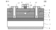


Classifications
-
- H—ELECTRICITY
- H10—SEMICONDUCTOR DEVICES; ELECTRIC SOLID-STATE DEVICES NOT OTHERWISE PROVIDED FOR
- H10F—INORGANIC SEMICONDUCTOR DEVICES SENSITIVE TO INFRARED RADIATION, LIGHT, ELECTROMAGNETIC RADIATION OF SHORTER WAVELENGTH OR CORPUSCULAR RADIATION
- H10F77/00—Constructional details of devices covered by this subclass
- H10F77/40—Optical elements or arrangements
- H10F77/413—Optical elements or arrangements directly associated or integrated with the devices, e.g. back reflectors
-
- H—ELECTRICITY
- H10—SEMICONDUCTOR DEVICES; ELECTRIC SOLID-STATE DEVICES NOT OTHERWISE PROVIDED FOR
- H10F—INORGANIC SEMICONDUCTOR DEVICES SENSITIVE TO INFRARED RADIATION, LIGHT, ELECTROMAGNETIC RADIATION OF SHORTER WAVELENGTH OR CORPUSCULAR RADIATION
- H10F30/00—Individual radiation-sensitive semiconductor devices in which radiation controls the flow of current through the devices, e.g. photodetectors
- H10F30/20—Individual radiation-sensitive semiconductor devices in which radiation controls the flow of current through the devices, e.g. photodetectors the devices having potential barriers, e.g. phototransistors
- H10F30/21—Individual radiation-sensitive semiconductor devices in which radiation controls the flow of current through the devices, e.g. photodetectors the devices having potential barriers, e.g. phototransistors the devices being sensitive to infrared, visible or ultraviolet radiation
- H10F30/22—Individual radiation-sensitive semiconductor devices in which radiation controls the flow of current through the devices, e.g. photodetectors the devices having potential barriers, e.g. phototransistors the devices being sensitive to infrared, visible or ultraviolet radiation the devices having only one potential barrier, e.g. photodiodes
- H10F30/221—Individual radiation-sensitive semiconductor devices in which radiation controls the flow of current through the devices, e.g. photodetectors the devices having potential barriers, e.g. phototransistors the devices being sensitive to infrared, visible or ultraviolet radiation the devices having only one potential barrier, e.g. photodiodes the potential barrier being a PN homojunction
- H10F30/2215—Individual radiation-sensitive semiconductor devices in which radiation controls the flow of current through the devices, e.g. photodetectors the devices having potential barriers, e.g. phototransistors the devices being sensitive to infrared, visible or ultraviolet radiation the devices having only one potential barrier, e.g. photodiodes the potential barrier being a PN homojunction the devices comprising active layers made of only Group III-V materials
-
- H—ELECTRICITY
- H10—SEMICONDUCTOR DEVICES; ELECTRIC SOLID-STATE DEVICES NOT OTHERWISE PROVIDED FOR
- H10F—INORGANIC SEMICONDUCTOR DEVICES SENSITIVE TO INFRARED RADIATION, LIGHT, ELECTROMAGNETIC RADIATION OF SHORTER WAVELENGTH OR CORPUSCULAR RADIATION
- H10F30/00—Individual radiation-sensitive semiconductor devices in which radiation controls the flow of current through the devices, e.g. photodetectors
- H10F30/20—Individual radiation-sensitive semiconductor devices in which radiation controls the flow of current through the devices, e.g. photodetectors the devices having potential barriers, e.g. phototransistors
- H10F30/21—Individual radiation-sensitive semiconductor devices in which radiation controls the flow of current through the devices, e.g. photodetectors the devices having potential barriers, e.g. phototransistors the devices being sensitive to infrared, visible or ultraviolet radiation
- H10F30/22—Individual radiation-sensitive semiconductor devices in which radiation controls the flow of current through the devices, e.g. photodetectors the devices having potential barriers, e.g. phototransistors the devices being sensitive to infrared, visible or ultraviolet radiation the devices having only one potential barrier, e.g. photodiodes
- H10F30/222—Individual radiation-sensitive semiconductor devices in which radiation controls the flow of current through the devices, e.g. photodetectors the devices having potential barriers, e.g. phototransistors the devices being sensitive to infrared, visible or ultraviolet radiation the devices having only one potential barrier, e.g. photodiodes the potential barrier being a PN heterojunction
-
- H—ELECTRICITY
- H10—SEMICONDUCTOR DEVICES; ELECTRIC SOLID-STATE DEVICES NOT OTHERWISE PROVIDED FOR
- H10F—INORGANIC SEMICONDUCTOR DEVICES SENSITIVE TO INFRARED RADIATION, LIGHT, ELECTROMAGNETIC RADIATION OF SHORTER WAVELENGTH OR CORPUSCULAR RADIATION
- H10F77/00—Constructional details of devices covered by this subclass
- H10F77/10—Semiconductor bodies
- H10F77/14—Shape of semiconductor bodies; Shapes, relative sizes or dispositions of semiconductor regions within semiconductor bodies
-
- H—ELECTRICITY
- H10—SEMICONDUCTOR DEVICES; ELECTRIC SOLID-STATE DEVICES NOT OTHERWISE PROVIDED FOR
- H10F—INORGANIC SEMICONDUCTOR DEVICES SENSITIVE TO INFRARED RADIATION, LIGHT, ELECTROMAGNETIC RADIATION OF SHORTER WAVELENGTH OR CORPUSCULAR RADIATION
- H10F77/00—Constructional details of devices covered by this subclass
- H10F77/30—Coatings
- H10F77/306—Coatings for devices having potential barriers
Landscapes
- Light Receiving Elements (AREA)
Applications Claiming Priority (1)
| Application Number | Priority Date | Filing Date | Title |
|---|---|---|---|
| PCT/JP2020/007584 WO2021171393A1 (ja) | 2020-02-26 | 2020-02-26 | 導波路型受光素子 |
Publications (3)
| Publication Number | Publication Date |
|---|---|
| JPWO2021171393A1 JPWO2021171393A1 (https=) | 2021-09-02 |
| JPWO2021171393A5 JPWO2021171393A5 (https=) | 2022-08-15 |
| JP7350974B2 true JP7350974B2 (ja) | 2023-09-26 |
Family
ID=77490804
Family Applications (1)
| Application Number | Title | Priority Date | Filing Date |
|---|---|---|---|
| JP2022502634A Active JP7350974B2 (ja) | 2020-02-26 | 2020-02-26 | 導波路型受光素子 |
Country Status (4)
| Country | Link |
|---|---|
| US (1) | US11978812B2 (https=) |
| JP (1) | JP7350974B2 (https=) |
| CN (1) | CN115136327B (https=) |
| WO (1) | WO2021171393A1 (https=) |
Families Citing this family (3)
| Publication number | Priority date | Publication date | Assignee | Title |
|---|---|---|---|---|
| JP7679259B2 (ja) * | 2021-08-20 | 2025-05-19 | 浜松ホトニクス株式会社 | 光検出器 |
| WO2023192918A2 (en) | 2022-03-29 | 2023-10-05 | Ostentus Therapeutics, Inc. | Anti-oncogenic phytochemicals and methods and uses for treating cancer |
| CN117199155B (zh) * | 2023-11-06 | 2024-02-13 | 杭州特洛伊光电技术有限公司 | 一种波导型可见光及近红外光探测器结构与制备方法 |
Citations (1)
| Publication number | Priority date | Publication date | Assignee | Title |
|---|---|---|---|---|
| CN108010982A (zh) | 2017-12-01 | 2018-05-08 | 北京工业大学 | 波导复合式耦合型单行载流子探测器 |
Family Cites Families (12)
| Publication number | Priority date | Publication date | Assignee | Title |
|---|---|---|---|---|
| JP3505186B2 (ja) * | 1996-06-13 | 2004-03-08 | 古河電気工業株式会社 | 半導体導波路型受光素子とその製造方法 |
| JP2965139B2 (ja) * | 1996-06-20 | 1999-10-18 | 日本電気株式会社 | 導波路型半導体受光素子 |
| JP2970575B2 (ja) * | 1997-03-06 | 1999-11-02 | 日本電気株式会社 | 導波路型半導体受光素子 |
| JP3111982B2 (ja) * | 1998-05-28 | 2000-11-27 | 日本電気株式会社 | 導波路型半導体光素子 |
| US6417528B1 (en) | 2000-01-28 | 2002-07-09 | Agere Systems Guardian Corp. | High speed semiconductor photodetector |
| JP2006066488A (ja) * | 2004-08-25 | 2006-03-09 | Mitsubishi Electric Corp | 半導体受光素子およびその製造方法 |
| JP2010512664A (ja) * | 2006-12-11 | 2010-04-22 | ルーメンツ リミテッド ライアビリティ カンパニー | 酸化亜鉛多接合光電池及び光電子装置 |
| JP5294558B2 (ja) * | 2006-12-19 | 2013-09-18 | 三菱電機株式会社 | 埋込導波路型受光素子とその製造方法 |
| US7919349B2 (en) * | 2008-02-22 | 2011-04-05 | Alcatel-Lucent Usa Inc. | Photonic integration scheme |
| JP2010010450A (ja) | 2008-06-27 | 2010-01-14 | Mitsubishi Electric Corp | 導波路型受光素子 |
| CN105122469B (zh) * | 2013-04-19 | 2017-03-08 | 富士通株式会社 | 半导体受光元件及其制造方法 |
| JP2019016694A (ja) * | 2017-07-06 | 2019-01-31 | 富士通株式会社 | 受光装置、これを用いた光受信器、及び受光装置の製造方法 |
-
2020
- 2020-02-26 JP JP2022502634A patent/JP7350974B2/ja active Active
- 2020-02-26 US US17/785,318 patent/US11978812B2/en active Active
- 2020-02-26 WO PCT/JP2020/007584 patent/WO2021171393A1/ja not_active Ceased
- 2020-02-26 CN CN202080097215.3A patent/CN115136327B/zh active Active
Patent Citations (1)
| Publication number | Priority date | Publication date | Assignee | Title |
|---|---|---|---|---|
| CN108010982A (zh) | 2017-12-01 | 2018-05-08 | 北京工业大学 | 波导复合式耦合型单行载流子探测器 |
Non-Patent Citations (1)
| Title |
|---|
| Y.-S. Wu et al.,"High-Performance Evanescently Edge Coupled Photodiodes With Partially p-Doped Photoabsorption Layer at 1.55-μm Wavelength",IEEE PHOTONICS TECHNOLOGY LETTERS,2005年04月,VOL. 17, NO. 4,pp.878-880 |
Also Published As
| Publication number | Publication date |
|---|---|
| CN115136327B (zh) | 2024-07-30 |
| WO2021171393A1 (ja) | 2021-09-02 |
| US11978812B2 (en) | 2024-05-07 |
| US20230055105A1 (en) | 2023-02-23 |
| JPWO2021171393A1 (https=) | 2021-09-02 |
| CN115136327A (zh) | 2022-09-30 |
Similar Documents
| Publication | Publication Date | Title |
|---|---|---|
| EP0800219B1 (en) | Heterojunction pin photodiode | |
| JP3141847B2 (ja) | アバランシェフォトダイオード | |
| JP7350974B2 (ja) | 導波路型受光素子 | |
| JP2708409B2 (ja) | 半導体受光素子およびその製造方法 | |
| CN101752446A (zh) | 雪崩光电二极管 | |
| CN112563351A (zh) | 一种大功率InGaAs/InP单行载流子光电探测器的设计方法 | |
| JP2941349B2 (ja) | 超格子apd | |
| JP2006040919A (ja) | アバランシェフォトダイオード | |
| US4587544A (en) | Avalanche photodetector | |
| JP2015149332A (ja) | アバランシ・フォトダイオード | |
| US20250318286A1 (en) | Semiconductor light receiving element | |
| US20250344548A1 (en) | Semiconductor light-receiving element | |
| GB2634166A (en) | Semiconductor light-receiving element | |
| JP2006229156A (ja) | フォトダイオード | |
| US20230253516A1 (en) | Photodetector | |
| JP3739273B2 (ja) | 半導体光検出器 | |
| US12495625B2 (en) | High-speed, large-area separate absorption and drift photodetector | |
| US12278304B2 (en) | High modulation speed PIN-type photodiode | |
| JP2739824B2 (ja) | 半導体受光素子 | |
| JP4284781B2 (ja) | Msm型フォトダイオード | |
| WO2024154204A1 (ja) | 裏面入射型受光素子 | |
| JP3147133B2 (ja) | 横型受光素子及びその形成方法 | |
| JP2742358B2 (ja) | 半導体光検出器およびその製造方法 | |
| KR100198423B1 (ko) | 애벌란치 광 다이오드형 장파장 광검출기 | |
| JP2893092B2 (ja) | アバランシェフォトダイオード |
Legal Events
| Date | Code | Title | Description |
|---|---|---|---|
| A521 | Request for written amendment filed |
Free format text: JAPANESE INTERMEDIATE CODE: A523 Effective date: 20220616 |
|
| A621 | Written request for application examination |
Free format text: JAPANESE INTERMEDIATE CODE: A621 Effective date: 20220616 |
|
| TRDD | Decision of grant or rejection written | ||
| A01 | Written decision to grant a patent or to grant a registration (utility model) |
Free format text: JAPANESE INTERMEDIATE CODE: A01 Effective date: 20230816 |
|
| A61 | First payment of annual fees (during grant procedure) |
Free format text: JAPANESE INTERMEDIATE CODE: A61 Effective date: 20230913 |
|
| R151 | Written notification of patent or utility model registration |
Ref document number: 7350974 Country of ref document: JP Free format text: JAPANESE INTERMEDIATE CODE: R151 |