JP6830772B2 - 積層膜の製造装置、及び積層膜の製造方法 - Google Patents
積層膜の製造装置、及び積層膜の製造方法 Download PDFInfo
- Publication number
- JP6830772B2 JP6830772B2 JP2016153361A JP2016153361A JP6830772B2 JP 6830772 B2 JP6830772 B2 JP 6830772B2 JP 2016153361 A JP2016153361 A JP 2016153361A JP 2016153361 A JP2016153361 A JP 2016153361A JP 6830772 B2 JP6830772 B2 JP 6830772B2
- Authority
- JP
- Japan
- Prior art keywords
- substrate
- processed
- chamber
- transport
- transfer machine
- Prior art date
- Legal status (The legal status is an assumption and is not a legal conclusion. Google has not performed a legal analysis and makes no representation as to the accuracy of the status listed.)
- Active
Links
Images


Classifications
-
- H—ELECTRICITY
- H10—SEMICONDUCTOR DEVICES; ELECTRIC SOLID-STATE DEVICES NOT OTHERWISE PROVIDED FOR
- H10K—ORGANIC ELECTRIC SOLID-STATE DEVICES
- H10K71/00—Manufacture or treatment specially adapted for the organic devices covered by this subclass
- H10K71/10—Deposition of organic active material
- H10K71/16—Deposition of organic active material using physical vapour deposition [PVD], e.g. vacuum deposition or sputtering
-
- C—CHEMISTRY; METALLURGY
- C23—COATING METALLIC MATERIAL; COATING MATERIAL WITH METALLIC MATERIAL; CHEMICAL SURFACE TREATMENT; DIFFUSION TREATMENT OF METALLIC MATERIAL; COATING BY VACUUM EVAPORATION, BY SPUTTERING, BY ION IMPLANTATION OR BY CHEMICAL VAPOUR DEPOSITION, IN GENERAL; INHIBITING CORROSION OF METALLIC MATERIAL OR INCRUSTATION IN GENERAL
- C23C—COATING METALLIC MATERIAL; COATING MATERIAL WITH METALLIC MATERIAL; SURFACE TREATMENT OF METALLIC MATERIAL BY DIFFUSION INTO THE SURFACE, BY CHEMICAL CONVERSION OR SUBSTITUTION; COATING BY VACUUM EVAPORATION, BY SPUTTERING, BY ION IMPLANTATION OR BY CHEMICAL VAPOUR DEPOSITION, IN GENERAL
- C23C14/00—Coating by vacuum evaporation, by sputtering or by ion implantation of the coating forming material
- C23C14/22—Coating by vacuum evaporation, by sputtering or by ion implantation of the coating forming material characterised by the process of coating
- C23C14/56—Apparatus specially adapted for continuous coating; Arrangements for maintaining the vacuum, e.g. vacuum locks
- C23C14/568—Transferring the substrates through a series of coating stations
-
- C—CHEMISTRY; METALLURGY
- C23—COATING METALLIC MATERIAL; COATING MATERIAL WITH METALLIC MATERIAL; CHEMICAL SURFACE TREATMENT; DIFFUSION TREATMENT OF METALLIC MATERIAL; COATING BY VACUUM EVAPORATION, BY SPUTTERING, BY ION IMPLANTATION OR BY CHEMICAL VAPOUR DEPOSITION, IN GENERAL; INHIBITING CORROSION OF METALLIC MATERIAL OR INCRUSTATION IN GENERAL
- C23C—COATING METALLIC MATERIAL; COATING MATERIAL WITH METALLIC MATERIAL; SURFACE TREATMENT OF METALLIC MATERIAL BY DIFFUSION INTO THE SURFACE, BY CHEMICAL CONVERSION OR SUBSTITUTION; COATING BY VACUUM EVAPORATION, BY SPUTTERING, BY ION IMPLANTATION OR BY CHEMICAL VAPOUR DEPOSITION, IN GENERAL
- C23C14/00—Coating by vacuum evaporation, by sputtering or by ion implantation of the coating forming material
- C23C14/06—Coating by vacuum evaporation, by sputtering or by ion implantation of the coating forming material characterised by the coating material
- C23C14/12—Organic material
-
- C—CHEMISTRY; METALLURGY
- C23—COATING METALLIC MATERIAL; COATING MATERIAL WITH METALLIC MATERIAL; CHEMICAL SURFACE TREATMENT; DIFFUSION TREATMENT OF METALLIC MATERIAL; COATING BY VACUUM EVAPORATION, BY SPUTTERING, BY ION IMPLANTATION OR BY CHEMICAL VAPOUR DEPOSITION, IN GENERAL; INHIBITING CORROSION OF METALLIC MATERIAL OR INCRUSTATION IN GENERAL
- C23C—COATING METALLIC MATERIAL; COATING MATERIAL WITH METALLIC MATERIAL; SURFACE TREATMENT OF METALLIC MATERIAL BY DIFFUSION INTO THE SURFACE, BY CHEMICAL CONVERSION OR SUBSTITUTION; COATING BY VACUUM EVAPORATION, BY SPUTTERING, BY ION IMPLANTATION OR BY CHEMICAL VAPOUR DEPOSITION, IN GENERAL
- C23C14/00—Coating by vacuum evaporation, by sputtering or by ion implantation of the coating forming material
- C23C14/22—Coating by vacuum evaporation, by sputtering or by ion implantation of the coating forming material characterised by the process of coating
- C23C14/24—Vacuum evaporation
-
- H—ELECTRICITY
- H01—ELECTRIC ELEMENTS
- H01L—SEMICONDUCTOR DEVICES NOT COVERED BY CLASS H10
- H01L21/00—Processes or apparatus adapted for the manufacture or treatment of semiconductor or solid state devices or of parts thereof
- H01L21/67—Apparatus specially adapted for handling semiconductor or electric solid state devices during manufacture or treatment thereof; Apparatus specially adapted for handling wafers during manufacture or treatment of semiconductor or electric solid state devices or components ; Apparatus not specifically provided for elsewhere
- H01L21/67005—Apparatus not specifically provided for elsewhere
- H01L21/67011—Apparatus for manufacture or treatment
- H01L21/67155—Apparatus for manufacturing or treating in a plurality of work-stations
- H01L21/67161—Apparatus for manufacturing or treating in a plurality of work-stations characterized by the layout of the process chambers
- H01L21/67173—Apparatus for manufacturing or treating in a plurality of work-stations characterized by the layout of the process chambers in-line arrangement
-
- H—ELECTRICITY
- H01—ELECTRIC ELEMENTS
- H01L—SEMICONDUCTOR DEVICES NOT COVERED BY CLASS H10
- H01L21/00—Processes or apparatus adapted for the manufacture or treatment of semiconductor or solid state devices or of parts thereof
- H01L21/67—Apparatus specially adapted for handling semiconductor or electric solid state devices during manufacture or treatment thereof; Apparatus specially adapted for handling wafers during manufacture or treatment of semiconductor or electric solid state devices or components ; Apparatus not specifically provided for elsewhere
- H01L21/67005—Apparatus not specifically provided for elsewhere
- H01L21/67011—Apparatus for manufacture or treatment
- H01L21/67155—Apparatus for manufacturing or treating in a plurality of work-stations
- H01L21/67184—Apparatus for manufacturing or treating in a plurality of work-stations characterized by the presence of more than one transfer chamber
-
- H—ELECTRICITY
- H01—ELECTRIC ELEMENTS
- H01L—SEMICONDUCTOR DEVICES NOT COVERED BY CLASS H10
- H01L21/00—Processes or apparatus adapted for the manufacture or treatment of semiconductor or solid state devices or of parts thereof
- H01L21/67—Apparatus specially adapted for handling semiconductor or electric solid state devices during manufacture or treatment thereof; Apparatus specially adapted for handling wafers during manufacture or treatment of semiconductor or electric solid state devices or components ; Apparatus not specifically provided for elsewhere
- H01L21/677—Apparatus specially adapted for handling semiconductor or electric solid state devices during manufacture or treatment thereof; Apparatus specially adapted for handling wafers during manufacture or treatment of semiconductor or electric solid state devices or components ; Apparatus not specifically provided for elsewhere for conveying, e.g. between different workstations
- H01L21/67739—Apparatus specially adapted for handling semiconductor or electric solid state devices during manufacture or treatment thereof; Apparatus specially adapted for handling wafers during manufacture or treatment of semiconductor or electric solid state devices or components ; Apparatus not specifically provided for elsewhere for conveying, e.g. between different workstations into and out of processing chamber
- H01L21/67745—Apparatus specially adapted for handling semiconductor or electric solid state devices during manufacture or treatment thereof; Apparatus specially adapted for handling wafers during manufacture or treatment of semiconductor or electric solid state devices or components ; Apparatus not specifically provided for elsewhere for conveying, e.g. between different workstations into and out of processing chamber characterized by movements or sequence of movements of transfer devices
-
- H—ELECTRICITY
- H01—ELECTRIC ELEMENTS
- H01L—SEMICONDUCTOR DEVICES NOT COVERED BY CLASS H10
- H01L21/00—Processes or apparatus adapted for the manufacture or treatment of semiconductor or solid state devices or of parts thereof
- H01L21/67—Apparatus specially adapted for handling semiconductor or electric solid state devices during manufacture or treatment thereof; Apparatus specially adapted for handling wafers during manufacture or treatment of semiconductor or electric solid state devices or components ; Apparatus not specifically provided for elsewhere
- H01L21/677—Apparatus specially adapted for handling semiconductor or electric solid state devices during manufacture or treatment thereof; Apparatus specially adapted for handling wafers during manufacture or treatment of semiconductor or electric solid state devices or components ; Apparatus not specifically provided for elsewhere for conveying, e.g. between different workstations
- H01L21/67739—Apparatus specially adapted for handling semiconductor or electric solid state devices during manufacture or treatment thereof; Apparatus specially adapted for handling wafers during manufacture or treatment of semiconductor or electric solid state devices or components ; Apparatus not specifically provided for elsewhere for conveying, e.g. between different workstations into and out of processing chamber
- H01L21/67748—Apparatus specially adapted for handling semiconductor or electric solid state devices during manufacture or treatment thereof; Apparatus specially adapted for handling wafers during manufacture or treatment of semiconductor or electric solid state devices or components ; Apparatus not specifically provided for elsewhere for conveying, e.g. between different workstations into and out of processing chamber horizontal transfer of a single workpiece
-
- H—ELECTRICITY
- H01—ELECTRIC ELEMENTS
- H01L—SEMICONDUCTOR DEVICES NOT COVERED BY CLASS H10
- H01L21/00—Processes or apparatus adapted for the manufacture or treatment of semiconductor or solid state devices or of parts thereof
- H01L21/67—Apparatus specially adapted for handling semiconductor or electric solid state devices during manufacture or treatment thereof; Apparatus specially adapted for handling wafers during manufacture or treatment of semiconductor or electric solid state devices or components ; Apparatus not specifically provided for elsewhere
- H01L21/677—Apparatus specially adapted for handling semiconductor or electric solid state devices during manufacture or treatment thereof; Apparatus specially adapted for handling wafers during manufacture or treatment of semiconductor or electric solid state devices or components ; Apparatus not specifically provided for elsewhere for conveying, e.g. between different workstations
- H01L21/67739—Apparatus specially adapted for handling semiconductor or electric solid state devices during manufacture or treatment thereof; Apparatus specially adapted for handling wafers during manufacture or treatment of semiconductor or electric solid state devices or components ; Apparatus not specifically provided for elsewhere for conveying, e.g. between different workstations into and out of processing chamber
- H01L21/67751—Apparatus specially adapted for handling semiconductor or electric solid state devices during manufacture or treatment thereof; Apparatus specially adapted for handling wafers during manufacture or treatment of semiconductor or electric solid state devices or components ; Apparatus not specifically provided for elsewhere for conveying, e.g. between different workstations into and out of processing chamber vertical transfer of a single workpiece
-
- H—ELECTRICITY
- H10—SEMICONDUCTOR DEVICES; ELECTRIC SOLID-STATE DEVICES NOT OTHERWISE PROVIDED FOR
- H10K—ORGANIC ELECTRIC SOLID-STATE DEVICES
- H10K59/00—Integrated devices, or assemblies of multiple devices, comprising at least one organic light-emitting element covered by group H10K50/00
- H10K59/10—OLED displays
- H10K59/12—Active-matrix OLED [AMOLED] displays
- H10K59/122—Pixel-defining structures or layers, e.g. banks
-
- H—ELECTRICITY
- H10—SEMICONDUCTOR DEVICES; ELECTRIC SOLID-STATE DEVICES NOT OTHERWISE PROVIDED FOR
- H10K—ORGANIC ELECTRIC SOLID-STATE DEVICES
- H10K71/00—Manufacture or treatment specially adapted for the organic devices covered by this subclass
-
- H—ELECTRICITY
- H10—SEMICONDUCTOR DEVICES; ELECTRIC SOLID-STATE DEVICES NOT OTHERWISE PROVIDED FOR
- H10K—ORGANIC ELECTRIC SOLID-STATE DEVICES
- H10K71/00—Manufacture or treatment specially adapted for the organic devices covered by this subclass
- H10K71/60—Forming conductive regions or layers, e.g. electrodes
-
- H—ELECTRICITY
- H10—SEMICONDUCTOR DEVICES; ELECTRIC SOLID-STATE DEVICES NOT OTHERWISE PROVIDED FOR
- H10K—ORGANIC ELECTRIC SOLID-STATE DEVICES
- H10K71/00—Manufacture or treatment specially adapted for the organic devices covered by this subclass
- H10K71/10—Deposition of organic active material
- H10K71/16—Deposition of organic active material using physical vapour deposition [PVD], e.g. vacuum deposition or sputtering
- H10K71/166—Deposition of organic active material using physical vapour deposition [PVD], e.g. vacuum deposition or sputtering using selective deposition, e.g. using a mask
Landscapes
- Engineering & Computer Science (AREA)
- Manufacturing & Machinery (AREA)
- Chemical & Material Sciences (AREA)
- Microelectronics & Electronic Packaging (AREA)
- General Physics & Mathematics (AREA)
- Condensed Matter Physics & Semiconductors (AREA)
- Computer Hardware Design (AREA)
- Power Engineering (AREA)
- Physics & Mathematics (AREA)
- Chemical Kinetics & Catalysis (AREA)
- Materials Engineering (AREA)
- Mechanical Engineering (AREA)
- Metallurgy (AREA)
- Organic Chemistry (AREA)
- Electroluminescent Light Sources (AREA)
- Physical Vapour Deposition (AREA)
- Chemical Vapour Deposition (AREA)
Description
Claims (17)
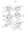
- 第1受渡室を介して接続された、第1及び第2移載機を有する主搬送路と、
前記第1又は第2移載機に接続された第2受渡室、及び前記第2受渡室に接続された搬送室とを有し、前記主搬送路と交差する方向に延在する副搬送路と、
前記搬送室に接続された、複数の第1処理室と、を有し、
前記主搬送路は、被処理基板を水平な状態で搬送されるように構成され、
前記複数の第1処理室の一は、処理中に前記被処理基板を垂直な状態で保持するように構成され、
前記搬送室は、前記被処理基板を搬送するためのアームを有し、
前記アームは、前記被処理基板を水平な状態と垂直な状態との間で転回させるための回転軸を有することを特徴とする、積層膜の製造装置。 - 前記複数の第1処理室の他の一は、処理中に前記被処理基板を水平な状態で保持するように構成されたことを特徴とする、請求項1に記載の製造装置。
- 第1受渡室を介して接続された、第1及び第2移載機を有する主搬送路と、
前記第1移載機に接続された第2受渡室、及び前記第2受渡室に接続された第1搬送室とを有し、前記主搬送路と交差する方向に延在する第1副搬送路と、
前記第2移載機に接続された第3受渡室、及び前記第3受渡室に接続された第2搬送室とを有し、前記主搬送路と交差する方向に延在する第2副搬送路と、
前記第1搬送室に接続された複数の第1処理室と、
前記第2搬送室に接続された複数の第2処理室と、を有し、
前記主搬送路は、被処理基板を水平な状態で搬送するように構成され、
前記複数の第1処理室の一は、処理中に前記被処理基板を垂直な状態で保持するように構成され、
前記複数の第2処理室の一は、処理中に前記被処理基板を水平な状態で保持するように構成され、
前記第1搬送室、及び前記第2搬送室はそれぞれ、前記被処理基板を搬送するためのアームを有し、
前記アームは、前記被処理基板を水平な状態と垂直な状態との間で転回させるための回転軸を有することを特徴とする、積層膜の製造装置。 - 前記第1移載機及び前記第2移載機はそれぞれ、
前記第1受渡室が接続される第1ポートと、前記第2受渡室が接続される第2ポートと、前記被処理基板を格納するバッファが接続される第3ポートと、を有し、
前記第1搬送室は、前記第2受渡室が接続される第4ポートと、前記複数の第1処理室の一が接続される第5ポートと、を有することを特徴とする、請求項3に記載の製造装置。 - 前記第1移載機及び前記第2移載機はそれぞれ、
前記第1受渡室が接続される第1ポートと、前記第2受渡室が接続される第2ポートと、前記被処理基板を格納するバッファが接続される第3ポートと、を有し、
前記第1搬送室及び前記第2搬送室はそれぞれ、前記第2受渡室が接続される第4ポートと、前記複数の第1処理室の一、又は前記複数の第2処理室の一が接続される第5ポートと、を有することを特徴とする、請求項3に記載の製造装置。 - 前記複数の第1処理室は、前記搬送室を中心として、放射状に前記搬送室に接続されることを特徴とする、請求項1又は請求項2に記載の製造装置。
- 前記複数の第1処理室は、前記第1搬送室を中心として、放射状に前記第1搬送室に接続され、
前記複数の第2処理室は、前記第2搬送室を中心として、放射状に前記第2搬送室に接続されることを特徴とする、請求項3に記載の製造装置。 - 前記第1乃至第5ポートはそれぞれ、気密性を有することを特徴とする、請求項4又は請求項5に記載の製造装置。
- 前記主搬送路上の末端に位置する前記第1移載機又は前記第2移載機に、他の第1受渡室を介して接続された基板投入取出口をさらに有し、
前記基板投入取出口は、処理前の前記被処理基板、および処理後の前記被処理基板が前記基板投入取出口を介して投入/取出できるように構成される、請求項1に記載の製造装置。 - 前記主搬送路上の一の末端に位置する前記第1移載機又は前記第2移載機に、基板投入口をさらに有し、
前記主搬送路上の他の末端に位置する前記第2移載機又は第1移載機に、基板取出口をさらに有し、
前記基板投入口は、処理前の前記被処理基板が前記基板投入口を介して投入できるように構成され、
前記基板取出口は、処理後の前記被処理基板が前記基板取出口を介して取出できるように構成される、請求項1に記載の製造装置。 - 前記主搬送路上の前記第1移載機又は前記第2移載機の前記第1ポートに、他の第1受渡室を介して接続された基板投入取出口をさらに有し、
前記主搬送路は、前記第1移載機、前記第1受渡室、前記第2移載機、及び前記基板投入取出口を通る環状経路を有し、
前記基板投入取出口は、処理前の前記被処理基板、および処理後の前記被処理基板が前記基板投入取出口を介して投入/取出できるように構成される、請求項4に記載の製造装置。 - 前記主搬送路は、一筆書き形状であることを特徴とする、請求項1乃至請求項10のいずれか一に記載の製造装置。
- 前記第1受渡室は、複数の前記被処理基板が互いにすれ違うように構成された、少なくとも二つのコンベアを備えることを特徴とする、請求項1乃至請求項10のいずれか一に記載の製造装置。
- 第1受渡室を介して接続された、第1及び第2移載機を有する主搬送路と、
前記第1又は第2移載機に接続された第2受渡室、及び前記第2受渡室に接続された搬送室とを有し、前記主搬送路と交差する方向に延在する副搬送路と、
前記搬送室に接続された、複数の第1処理室と、を有する製造装置を用いた積層膜の製造方法であって、
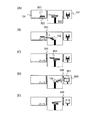
絶縁表面を有し、前記絶縁表面上の画素電極と、前記画素電極の端部を覆うと共に、前記画素電極の上面の一部を露出するバンクと、を有する被処理基板を用意し、
前記被処理基板を、前記製造装置の前記主搬送路上に設けられた前記第1移載機に搬入し、
前記被処理基板を、前記第1移載機から、前記第2受渡室を介して前記搬送室に搬入し、
前記被処理基板を、前記搬送室から前記複数の第1処理室の一に搬入し、
前記被処理基板を水平な状態に保持して、前記画素電極及び前記バンク上に第1有機層を形成し、
前記被処理基板を、前記複数の第1処理室の一から前記搬送室に戻し、
前記搬送室内で、前記被処理基板を水平な状態から垂直な状態に転回し、
前記被処理基板を、前記搬送室から前記複数の第1処理室の他の一に搬入し、
前記被処理基板を垂直な状態に保持して、前記第1有機層上の、前記画素電極に重畳する領域に第2有機層を形成し、
前記被処理基板を、前記複数の第1処理室の他の一から前記搬送室に戻し、
前記搬送室内で、前記被処理基板を垂直な状態から水平な状態に転回し、
前記被処理基板を、前記搬送室から、前記第2受渡室を介して前記第1移載機に戻す工程を含む、積層膜の製造方法。 - 第1受渡室を介して接続された、第1及び第2移載機を有する主搬送路と、
前記第1移載機に接続された第2受渡室、及び前記第2受渡室に接続された第1搬送室とを有し、前記主搬送路と交差する方向に延在する第1副搬送路と、
前記第2移載機に接続された第3受渡室、及び前記第3受渡室に接続された第2搬送室とを有し、前記主搬送路と交差する方向に延在する第2副搬送路と、
前記第1搬送室に接続された複数の第1処理室と、
前記第2搬送室に接続された複数の第2処理室と、を有する製造装置を用いた積層膜の製造方法であって、
絶縁表面上に、画素電極と、前記画素電極の端部を覆うと共に、前記画素電極の上面の一部を露出するバンクと、を有する被処理基板を用意し、
前記被処理基板を、前記製造装置の前記主搬送路上に設けられた前記第1移載機に搬入し、
前記被処理基板を、前記第1移載機から、前記第2受渡室を介して前記第1搬送室に搬入し、
前記被処理基板を、前記第1搬送室から前記複数の第1処理室の一に搬入し、
前記被処理基板を水平な状態に保持して、前記画素電極及び前記バンク上に第1有機層を形成し、
前記被処理基板を、前記複数の第1処理室の一から前記第1搬送室に戻し、
前記被処理基板を、前記第1搬送室から、前記第2受渡室を介して前記第1移載機に戻し、
前記被処理基板を、前記第1移載機から、前記第1受渡室を介して前記第2移載機に搬入し、
前記被処理基板を、前記第2移載機から、前記第3受渡室を介して前記第2搬送室に搬入し、
前記第2搬送室内で、前記被処理基板を水平な状態から垂直な状態に転回し、
前記被処理基板を、前記第2搬送室から前記複数の第2処理室の一に搬入し、
前記被処理基板を垂直な状態に保持して、前記第1有機層上の、前記画素電極に重畳する領域に第2有機層を形成し、
前記被処理基板を、前記第2処理室の一から前記第2搬送室に戻し、
前記第2搬送室内で、前記被処理基板を垂直な状態から水平な状態に転回し、
前記被処理基板を、前記第2搬送室から、前記第3受渡室を介して前記第2移載機に戻す工程を含む、積層膜の製造方法。 - 前記第1有機層は、発光素子のホール輸送層又は電子輸送層を含むことを特徴とする、請求項14又は請求項15に記載の製造方法。
- 前記第2有機層は、発光素子の発光層を含むことを特徴とする、請求項14又は請求項15に記載の製造方法。
Priority Applications (9)
| Application Number | Priority Date | Filing Date | Title |
|---|---|---|---|
| JP2016153361A JP6830772B2 (ja) | 2016-08-04 | 2016-08-04 | 積層膜の製造装置、及び積層膜の製造方法 |
| TW106114597A TWI671918B (zh) | 2016-08-04 | 2017-05-03 | 發光元件之製造裝置及其製造方法 |
| KR1020170082506A KR101953268B1 (ko) | 2016-08-04 | 2017-06-29 | 발광 소자의 제조 장치 및 그 제조 방법 |
| US15/644,923 US10164218B2 (en) | 2016-08-04 | 2017-07-10 | Manufacturing device and manufacturing method of light-emitting element |
| CN202010289273.8A CN111463365B (zh) | 2016-08-04 | 2017-08-04 | 发光元件的制造装置和制造方法 |
| CN201710662741.XA CN107689429A (zh) | 2016-08-04 | 2017-08-04 | 发光元件的制造装置和制造方法 |
| US16/162,528 US10367174B2 (en) | 2016-08-04 | 2018-10-17 | Manufacturing method of a light emitting device |
| KR1020190021103A KR102039090B1 (ko) | 2016-08-04 | 2019-02-22 | 발광 소자의 제조 방법 |
| US16/447,478 US20190305259A1 (en) | 2016-08-04 | 2019-06-20 | Manufacturing device for light emitting element |
Applications Claiming Priority (1)
| Application Number | Priority Date | Filing Date | Title |
|---|---|---|---|
| JP2016153361A JP6830772B2 (ja) | 2016-08-04 | 2016-08-04 | 積層膜の製造装置、及び積層膜の製造方法 |
Publications (3)
| Publication Number | Publication Date |
|---|---|
| JP2018022619A JP2018022619A (ja) | 2018-02-08 |
| JP2018022619A5 JP2018022619A5 (ja) | 2019-09-05 |
| JP6830772B2 true JP6830772B2 (ja) | 2021-02-17 |
Family
ID=61070200
Family Applications (1)
| Application Number | Title | Priority Date | Filing Date |
|---|---|---|---|
| JP2016153361A Active JP6830772B2 (ja) | 2016-08-04 | 2016-08-04 | 積層膜の製造装置、及び積層膜の製造方法 |
Country Status (5)
| Country | Link |
|---|---|
| US (3) | US10164218B2 (ja) |
| JP (1) | JP6830772B2 (ja) |
| KR (2) | KR101953268B1 (ja) |
| CN (2) | CN111463365B (ja) |
| TW (1) | TWI671918B (ja) |
Families Citing this family (8)
| Publication number | Priority date | Publication date | Assignee | Title |
|---|---|---|---|---|
| JP6830772B2 (ja) * | 2016-08-04 | 2021-02-17 | 株式会社ジャパンディスプレイ | 積層膜の製造装置、及び積層膜の製造方法 |
| WO2019170252A1 (en) * | 2018-03-09 | 2019-09-12 | Applied Materials, Inc. | Vacuum processing system and method of operating a vacuum processing system |
| KR20200002242A (ko) * | 2018-06-29 | 2020-01-08 | 캐논 톡키 가부시키가이샤 | 성막 장치, 유기 디바이스의 제조 장치, 및 유기 디바이스의 제조 방법 |
| JP7240980B2 (ja) * | 2019-07-29 | 2023-03-16 | 東京エレクトロン株式会社 | 基板処理装置及び基板搬送方法 |
| TWI867219B (zh) * | 2020-05-12 | 2024-12-21 | 荷蘭商Asm Ip私人控股有限公司 | 半導體處理系統 |
| US20240057462A1 (en) * | 2020-12-25 | 2024-02-15 | Semiconductor Energy Laboratory Co., Ltd. | Manufacturing equipment of display device |
| KR20240034778A (ko) * | 2021-07-16 | 2024-03-14 | 가부시키가이샤 한도오따이 에네루기 켄큐쇼 | 발광 디바이스의 제조 장치 |
| JP7747470B2 (ja) * | 2021-09-06 | 2025-10-01 | キヤノントッキ株式会社 | 成膜装置、基板搬送装置、基板搬送方法及び電子デバイスの製造方法 |
Family Cites Families (31)
| Publication number | Priority date | Publication date | Assignee | Title |
|---|---|---|---|---|
| JPH07211762A (ja) * | 1994-01-13 | 1995-08-11 | Hitachi Ltd | ウエハ搬送処理装置 |
| JPH07230942A (ja) * | 1994-02-18 | 1995-08-29 | Hitachi Ltd | マルチチャンバシステム及びその制御方法 |
| JPH08181184A (ja) * | 1994-12-22 | 1996-07-12 | Hitachi Ltd | 半導体製造ラインの構成方法 |
| TW442891B (en) * | 1998-11-17 | 2001-06-23 | Tokyo Electron Ltd | Vacuum processing system |
| JP3806802B2 (ja) * | 2001-04-25 | 2006-08-09 | 株式会社アイテック | ロボットハンドの駆動装置 |
| US6852194B2 (en) * | 2001-05-21 | 2005-02-08 | Tokyo Electron Limited | Processing apparatus, transferring apparatus and transferring method |
| JP4078813B2 (ja) * | 2001-06-12 | 2008-04-23 | ソニー株式会社 | 成膜装置および成膜方法 |
| JP4096353B2 (ja) * | 2002-05-09 | 2008-06-04 | ソニー株式会社 | 有機電界発光表示素子の製造装置および製造方法 |
| US7988398B2 (en) * | 2002-07-22 | 2011-08-02 | Brooks Automation, Inc. | Linear substrate transport apparatus |
| CN2587883Y (zh) * | 2002-12-19 | 2003-11-26 | 铼宝科技股份有限公司 | 有机发光组件的沉积设备 |
| JP2004288463A (ja) * | 2003-03-20 | 2004-10-14 | Semiconductor Energy Lab Co Ltd | 製造装置 |
| JP5226215B2 (ja) * | 2003-11-10 | 2013-07-03 | ブルックス オートメーション インコーポレイテッド | 真空下の半導体処理システムにおいて加工中の製品を処理する方法及びシステム |
| US8313277B2 (en) * | 2003-11-10 | 2012-11-20 | Brooks Automation, Inc. | Semiconductor manufacturing process modules |
| JP5128918B2 (ja) * | 2007-11-30 | 2013-01-23 | 株式会社Sokudo | 基板処理装置 |
| US9353436B2 (en) * | 2008-03-05 | 2016-05-31 | Applied Materials, Inc. | Coating apparatus with rotation module |
| KR20100132517A (ko) | 2008-03-05 | 2010-12-17 | 어플라이드 머티어리얼스, 인코포레이티드 | 회전 모듈을 갖는 코팅 장치 |
| JP4934619B2 (ja) * | 2008-03-17 | 2012-05-16 | 株式会社アルバック | 有機el製造装置及び有機el製造方法 |
| TW201408133A (zh) * | 2008-09-04 | 2014-02-16 | Hitachi High Tech Corp | 有機電激發光裝置製造裝置及其製造方法以及成膜裝置及成膜方法 |
| CN101667630A (zh) * | 2008-09-04 | 2010-03-10 | 株式会社日立高新技术 | 有机el设备制造装置和其制造方法以及成膜装置和成膜方法 |
| US20110097518A1 (en) * | 2009-10-28 | 2011-04-28 | Applied Materials, Inc. | Vertically integrated processing chamber |
| EP2489759B1 (en) * | 2011-02-21 | 2014-12-10 | Applied Materials, Inc. | System for utilization improvement of process chambers and method of operating thereof |
| CN103930984B (zh) * | 2011-11-23 | 2016-09-21 | 日本电产三协株式会社 | 工件搬运系统 |
| WO2013090181A1 (en) * | 2011-12-12 | 2013-06-20 | Applied Materials, Inc | Fully-independent robot systems, apparatus, and methods adapted to transport multiple substrates in electronic device manufacturing |
| KR20130074307A (ko) * | 2011-12-26 | 2013-07-04 | 엘아이지에이디피 주식회사 | 척킹 및 디척킹 장치부를 갖는 유기발광소자 양산 시스템 |
| JP6079200B2 (ja) * | 2012-05-16 | 2017-02-15 | 東京エレクトロン株式会社 | クーリング機構及び処理システム |
| KR20140050994A (ko) * | 2012-10-22 | 2014-04-30 | 삼성디스플레이 주식회사 | 유기 발광 디스플레이 장치 및 그 제조 방법 |
| KR101990555B1 (ko) * | 2012-12-24 | 2019-06-19 | 삼성디스플레이 주식회사 | 박막봉지 제조장치 및 박막봉지 제조방법 |
| JP2015007263A (ja) * | 2013-06-24 | 2015-01-15 | 株式会社日立ハイテクノロジーズ | 有機デバイス製造装置および有機デバイスの製造方法 |
| KR20160087953A (ko) * | 2015-01-14 | 2016-07-25 | 에스엔유 프리시젼 주식회사 | 유기발광소자 제조용 클러스터 타입 증착장치 |
| JP6937549B2 (ja) * | 2016-06-10 | 2021-09-22 | 株式会社ジャパンディスプレイ | 発光素子の製造装置 |
| JP6830772B2 (ja) * | 2016-08-04 | 2021-02-17 | 株式会社ジャパンディスプレイ | 積層膜の製造装置、及び積層膜の製造方法 |
-
2016
- 2016-08-04 JP JP2016153361A patent/JP6830772B2/ja active Active
-
2017
- 2017-05-03 TW TW106114597A patent/TWI671918B/zh active
- 2017-06-29 KR KR1020170082506A patent/KR101953268B1/ko active Active
- 2017-07-10 US US15/644,923 patent/US10164218B2/en active Active
- 2017-08-04 CN CN202010289273.8A patent/CN111463365B/zh active Active
- 2017-08-04 CN CN201710662741.XA patent/CN107689429A/zh active Pending
-
2018
- 2018-10-17 US US16/162,528 patent/US10367174B2/en active Active
-
2019
- 2019-02-22 KR KR1020190021103A patent/KR102039090B1/ko active Active
- 2019-06-20 US US16/447,478 patent/US20190305259A1/en not_active Abandoned
Also Published As
| Publication number | Publication date |
|---|---|
| KR102039090B1 (ko) | 2019-11-01 |
| US10367174B2 (en) | 2019-07-30 |
| US20180040856A1 (en) | 2018-02-08 |
| US20190051867A1 (en) | 2019-02-14 |
| KR101953268B1 (ko) | 2019-02-28 |
| KR20180016253A (ko) | 2018-02-14 |
| KR20190022594A (ko) | 2019-03-06 |
| JP2018022619A (ja) | 2018-02-08 |
| TW201806178A (zh) | 2018-02-16 |
| CN107689429A (zh) | 2018-02-13 |
| CN111463365A (zh) | 2020-07-28 |
| TWI671918B (zh) | 2019-09-11 |
| CN111463365B (zh) | 2023-05-26 |
| US20190305259A1 (en) | 2019-10-03 |
| US10164218B2 (en) | 2018-12-25 |
Similar Documents
| Publication | Publication Date | Title |
|---|---|---|
| JP6830772B2 (ja) | 積層膜の製造装置、及び積層膜の製造方法 | |
| JP6937549B2 (ja) | 発光素子の製造装置 | |
| JP7148587B2 (ja) | 成膜装置、および電子デバイスの製造方法 | |
| US9644258B2 (en) | Apparatus and method of manufacturing display device | |
| KR101409808B1 (ko) | 기판처리시스템 | |
| JP2009170282A (ja) | 基板処理装置および有機エレクトロルミネッセンス装置の製造方法 | |
| CN100591799C (zh) | 成膜装置、薄膜的制造装置及成膜方法 | |
| KR101700608B1 (ko) | 기판처리장치 | |
| KR101225212B1 (ko) | Oled제조장치 및 방법 | |
| KR102413664B1 (ko) | 클러스터 증착 시스템 | |
| KR102430349B1 (ko) | 클러스터 증착 시스템 | |
| WO2011040538A1 (ja) | 基板処理システム | |
| KR101218972B1 (ko) | 기판처리시스템 | |
| KR20120074416A (ko) | 기판처리장치 및 방법 |
Legal Events
| Date | Code | Title | Description |
|---|---|---|---|
| A521 | Request for written amendment filed |
Free format text: JAPANESE INTERMEDIATE CODE: A523 Effective date: 20190726 |
|
| A621 | Written request for application examination |
Free format text: JAPANESE INTERMEDIATE CODE: A621 Effective date: 20190726 |
|
| A131 | Notification of reasons for refusal |
Free format text: JAPANESE INTERMEDIATE CODE: A131 Effective date: 20200714 |
|
| A601 | Written request for extension of time |
Free format text: JAPANESE INTERMEDIATE CODE: A601 Effective date: 20200910 |
|
| A521 | Request for written amendment filed |
Free format text: JAPANESE INTERMEDIATE CODE: A523 Effective date: 20201111 |
|
| TRDD | Decision of grant or rejection written | ||
| A01 | Written decision to grant a patent or to grant a registration (utility model) |
Free format text: JAPANESE INTERMEDIATE CODE: A01 Effective date: 20210105 |
|
| A61 | First payment of annual fees (during grant procedure) |
Free format text: JAPANESE INTERMEDIATE CODE: A61 Effective date: 20210127 |
|
| R150 | Certificate of patent or registration of utility model |
Ref document number: 6830772 Country of ref document: JP Free format text: JAPANESE INTERMEDIATE CODE: R150 |
|
| R250 | Receipt of annual fees |
Free format text: JAPANESE INTERMEDIATE CODE: R250 |
|
| R250 | Receipt of annual fees |
Free format text: JAPANESE INTERMEDIATE CODE: R250 |
|
| S111 | Request for change of ownership or part of ownership |
Free format text: JAPANESE INTERMEDIATE CODE: R313113 |
|
| R350 | Written notification of registration of transfer |
Free format text: JAPANESE INTERMEDIATE CODE: R350 |