JP6811202B2 - エッチングする方法及びプラズマ処理装置 - Google Patents
エッチングする方法及びプラズマ処理装置 Download PDFInfo
- Publication number
- JP6811202B2 JP6811202B2 JP2018079147A JP2018079147A JP6811202B2 JP 6811202 B2 JP6811202 B2 JP 6811202B2 JP 2018079147 A JP2018079147 A JP 2018079147A JP 2018079147 A JP2018079147 A JP 2018079147A JP 6811202 B2 JP6811202 B2 JP 6811202B2
- Authority
- JP
- Japan
- Prior art keywords
- region
- substrate
- film
- gas
- plasma
- Prior art date
- Legal status (The legal status is an assumption and is not a legal conclusion. Google has not performed a legal analysis and makes no representation as to the accuracy of the status listed.)
- Active
Links
Images


Classifications
-
- H—ELECTRICITY
- H01—ELECTRIC ELEMENTS
- H01J—ELECTRIC DISCHARGE TUBES OR DISCHARGE LAMPS
- H01J37/00—Discharge tubes with provision for introducing objects or material to be exposed to the discharge, e.g. for the purpose of examination or processing thereof
- H01J37/32—Gas-filled discharge tubes
- H01J37/32431—Constructional details of the reactor
-
- H—ELECTRICITY
- H10—SEMICONDUCTOR DEVICES; ELECTRIC SOLID-STATE DEVICES NOT OTHERWISE PROVIDED FOR
- H10P—GENERIC PROCESSES OR APPARATUS FOR THE MANUFACTURE OR TREATMENT OF DEVICES COVERED BY CLASS H10
- H10P50/00—Etching of wafers, substrates or parts of devices
- H10P50/20—Dry etching; Plasma etching; Reactive-ion etching
- H10P50/28—Dry etching; Plasma etching; Reactive-ion etching of insulating materials
- H10P50/282—Dry etching; Plasma etching; Reactive-ion etching of insulating materials of inorganic materials
- H10P50/283—Dry etching; Plasma etching; Reactive-ion etching of insulating materials of inorganic materials by chemical means
-
- H—ELECTRICITY
- H01—ELECTRIC ELEMENTS
- H01J—ELECTRIC DISCHARGE TUBES OR DISCHARGE LAMPS
- H01J37/00—Discharge tubes with provision for introducing objects or material to be exposed to the discharge, e.g. for the purpose of examination or processing thereof
- H01J37/32—Gas-filled discharge tubes
- H01J37/32009—Arrangements for generation of plasma specially adapted for examination or treatment of objects, e.g. plasma sources
-
- H—ELECTRICITY
- H01—ELECTRIC ELEMENTS
- H01J—ELECTRIC DISCHARGE TUBES OR DISCHARGE LAMPS
- H01J37/00—Discharge tubes with provision for introducing objects or material to be exposed to the discharge, e.g. for the purpose of examination or processing thereof
- H01J37/32—Gas-filled discharge tubes
- H01J37/32431—Constructional details of the reactor
- H01J37/3244—Gas supply means
-
- H—ELECTRICITY
- H05—ELECTRIC TECHNIQUES NOT OTHERWISE PROVIDED FOR
- H05H—PLASMA TECHNIQUE; PRODUCTION OF ACCELERATED ELECTRICALLY-CHARGED PARTICLES OR OF NEUTRONS; PRODUCTION OR ACCELERATION OF NEUTRAL MOLECULAR OR ATOMIC BEAMS
- H05H1/00—Generating plasma; Handling plasma
- H05H1/24—Generating plasma
- H05H1/46—Generating plasma using applied electromagnetic fields, e.g. high frequency or microwave energy
-
- H—ELECTRICITY
- H10—SEMICONDUCTOR DEVICES; ELECTRIC SOLID-STATE DEVICES NOT OTHERWISE PROVIDED FOR
- H10P—GENERIC PROCESSES OR APPARATUS FOR THE MANUFACTURE OR TREATMENT OF DEVICES COVERED BY CLASS H10
- H10P14/00—Formation of materials, e.g. in the shape of layers or pillars
- H10P14/60—Formation of materials, e.g. in the shape of layers or pillars of insulating materials
- H10P14/66—Formation of materials, e.g. in the shape of layers or pillars of insulating materials characterised by the type of materials
- H10P14/668—Formation of materials, e.g. in the shape of layers or pillars of insulating materials characterised by the type of materials the materials being characterised by the deposition precursor materials
-
- H—ELECTRICITY
- H10—SEMICONDUCTOR DEVICES; ELECTRIC SOLID-STATE DEVICES NOT OTHERWISE PROVIDED FOR
- H10P—GENERIC PROCESSES OR APPARATUS FOR THE MANUFACTURE OR TREATMENT OF DEVICES COVERED BY CLASS H10
- H10P14/00—Formation of materials, e.g. in the shape of layers or pillars
- H10P14/60—Formation of materials, e.g. in the shape of layers or pillars of insulating materials
- H10P14/69—Inorganic materials
- H10P14/692—Inorganic materials composed of oxides, glassy oxides or oxide-based glasses
- H10P14/6921—Inorganic materials composed of oxides, glassy oxides or oxide-based glasses containing silicon
- H10P14/69215—Inorganic materials composed of oxides, glassy oxides or oxide-based glasses containing silicon the material being a silicon oxide, e.g. SiO2
-
- H—ELECTRICITY
- H10—SEMICONDUCTOR DEVICES; ELECTRIC SOLID-STATE DEVICES NOT OTHERWISE PROVIDED FOR
- H10P—GENERIC PROCESSES OR APPARATUS FOR THE MANUFACTURE OR TREATMENT OF DEVICES COVERED BY CLASS H10
- H10P14/00—Formation of materials, e.g. in the shape of layers or pillars
- H10P14/60—Formation of materials, e.g. in the shape of layers or pillars of insulating materials
- H10P14/69—Inorganic materials
- H10P14/692—Inorganic materials composed of oxides, glassy oxides or oxide-based glasses
- H10P14/6921—Inorganic materials composed of oxides, glassy oxides or oxide-based glasses containing silicon
- H10P14/6922—Inorganic materials composed of oxides, glassy oxides or oxide-based glasses containing silicon the material containing Si, O and at least one of H, N, C, F or other non-metal elements, e.g. SiOC, SiOC:H or SiONC
-
- H—ELECTRICITY
- H10—SEMICONDUCTOR DEVICES; ELECTRIC SOLID-STATE DEVICES NOT OTHERWISE PROVIDED FOR
- H10P—GENERIC PROCESSES OR APPARATUS FOR THE MANUFACTURE OR TREATMENT OF DEVICES COVERED BY CLASS H10
- H10P50/00—Etching of wafers, substrates or parts of devices
- H10P50/20—Dry etching; Plasma etching; Reactive-ion etching
- H10P50/24—Dry etching; Plasma etching; Reactive-ion etching of semiconductor materials
- H10P50/242—Dry etching; Plasma etching; Reactive-ion etching of semiconductor materials of Group IV materials
-
- H—ELECTRICITY
- H10—SEMICONDUCTOR DEVICES; ELECTRIC SOLID-STATE DEVICES NOT OTHERWISE PROVIDED FOR
- H10P—GENERIC PROCESSES OR APPARATUS FOR THE MANUFACTURE OR TREATMENT OF DEVICES COVERED BY CLASS H10
- H10P50/00—Etching of wafers, substrates or parts of devices
- H10P50/20—Dry etching; Plasma etching; Reactive-ion etching
- H10P50/26—Dry etching; Plasma etching; Reactive-ion etching of conductive or resistive materials
- H10P50/264—Dry etching; Plasma etching; Reactive-ion etching of conductive or resistive materials by chemical means
- H10P50/266—Dry etching; Plasma etching; Reactive-ion etching of conductive or resistive materials by chemical means by vapour etching only
- H10P50/267—Dry etching; Plasma etching; Reactive-ion etching of conductive or resistive materials by chemical means by vapour etching only using plasmas
-
- H—ELECTRICITY
- H10—SEMICONDUCTOR DEVICES; ELECTRIC SOLID-STATE DEVICES NOT OTHERWISE PROVIDED FOR
- H10P—GENERIC PROCESSES OR APPARATUS FOR THE MANUFACTURE OR TREATMENT OF DEVICES COVERED BY CLASS H10
- H10P72/00—Handling or holding of wafers, substrates or devices during manufacture or treatment thereof
- H10P72/04—Apparatus for manufacture or treatment
- H10P72/0402—Apparatus for fluid treatment
- H10P72/0418—Apparatus for fluid treatment for etching
- H10P72/0421—Apparatus for fluid treatment for etching for drying etching
-
- H—ELECTRICITY
- H01—ELECTRIC ELEMENTS
- H01J—ELECTRIC DISCHARGE TUBES OR DISCHARGE LAMPS
- H01J2237/00—Discharge tubes exposing object to beam, e.g. for analysis treatment, etching, imaging
- H01J2237/32—Processing objects by plasma generation
- H01J2237/33—Processing objects by plasma generation characterised by the type of processing
- H01J2237/334—Etching
- H01J2237/3341—Reactive etching
Landscapes
- Physics & Mathematics (AREA)
- Engineering & Computer Science (AREA)
- Plasma & Fusion (AREA)
- Chemical & Material Sciences (AREA)
- Analytical Chemistry (AREA)
- Electromagnetism (AREA)
- Spectroscopy & Molecular Physics (AREA)
- Drying Of Semiconductors (AREA)
- Plasma Technology (AREA)
- Crystals, And After-Treatments Of Crystals (AREA)
Description
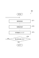
工程ST1
内部空間10sにおける圧力:20mTorr(2.666Pa)
第1の高周波電力:60MHz、100W
第2の高周波電力:40MHz、100W
CH3Fガスの流量/Arガスの流量:15sccm/200sccm
処理時間:5秒
工程ST2
内部空間10sにおける圧力:200mTorr(26.66Pa)
第1の高周波電力:0W
第2の高周波電力:0W
アミノシランガスの流量/Arガスの流量:100sccm/300sccm
処理時間:15秒
工程STb
内部空間10sにおける圧力:200mTorr(26.66Pa)
第1の高周波電力:0W
第2の高周波電力:0W
Arガスの流量:300sccm
処理時間:10秒
工程ST3
内部空間10sにおける圧力:20mTorr(2.666Pa)
第1の高周波電力:60MHz、100W
第2の高周波電力:40MHz、300W
Arガスの流量:200sccm
処理時間:5秒
Claims (16)
- 基板をエッチングする方法であって、
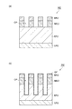
前記基板上に堆積膜を形成する工程であり、該堆積膜は第1のガスから生成されたプラズマに含まれる化学種から形成され、該基板は、第1領域及び該第1領域の材料とは異なる材料から形成された第2領域を有する、該工程と、
その上に前記堆積膜が形成された前記基板に、前駆体ガスを供給する工程であり、該前駆体ガスを用いて該基板上に吸着膜を形成する、該工程と、
その上に前記堆積膜及び前記吸着膜が形成された前記基板に第2のガスから生成されたプラズマからのイオンを供給して前記第1領域の前記材料と前記堆積膜に含まれる前記化学種とを反応させることにより、前記第2領域に対して選択的に前記第1領域をエッチングする工程であり、前記吸着膜によって前記第2領域のエッチングレートを減少させる、該工程と、
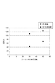
を含む方法。 - 前記吸着膜は、前記第2領域をエッチングする前記堆積膜中の化学種の量を減少させる、請求項1に記載の方法。
- 前記堆積膜は、炭素、水素、及びフッ素を含む、請求項1又は2に記載の方法。
- 前記第1領域は、窒化シリコンから形成されている、請求項3に記載の方法。
- 前記吸着膜は、前記第2領域をエッチングする前記堆積膜中のフッ素の量を減少させる、請求項3に記載の方法。
- 前記第1のガスは、ハイドロフルオロカーボンガスを含む、請求項1〜5の何れか一項に記載の方法。
- 前記ハイドロフルオロカーボンガスは、CH3Fガスを含む、請求項6に記載の方法。
- 前記第2領域は、シリコンを含む、請求項1〜7の何れか一項に記載の方法。
- 前記吸着膜は、シリコンを含む、請求項8に記載の方法。
- 前記前駆体ガスは、シリコン含有ガスである、請求項1〜9の何れか一項に記載の方法。
- 基板をエッチングする方法であって、
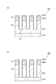
第1領域及び該第1領域とは異なる材料から形成された第2領域を有する基板を提供する工程と、
前記基板上に堆積膜を形成する工程と、
前記堆積膜がその上に形成された前記基板上に単分子の吸着膜を形成する工程と、
その上に前記堆積膜及び前記吸着膜が形成された前記基板にプラズマからのイオンを供給して前記第1領域の材料と前記堆積膜に含まれる化学種とを反応させることにより、前記第2領域に対して選択的に前記第1領域をエッチングする工程であり、前記吸着膜によって前記第2領域のエッチングレートを減少させる、該工程と、
を含む方法。 - 前記第1領域が前記基板において開口を画成する底部であり、前記第2領域が該開口を画成する側部であるように、前記基板に該開口を形成する工程を更に含む、請求項11に記載の方法。
- 前記基板は、前記第1領域及び前記第2領域を含む膜を含み、前記開口は該膜に形成される、請求項12に記載の方法。
- 前記膜は、シリコン酸化膜又はSiOCH膜である、請求項13に記載の方法。
- 前記堆積膜は、炭素及びフッ素を含み、前記吸着膜は、前記堆積膜におけるフッ素の量を減少させる、請求項11に記載の方法。
- 内部空間を有するチャンバと、
前記チャンバの前記内部空間の中で基板を支持する支持台と、
前記チャンバの前記内部空間に、第1のガス、第2のガス、及び前駆体ガスを含む複数のガスを供給するガス供給部と、
前記チャンバの前記内部空間の中のガスを励起させてプラズマを生成するプラズマ生成部と、
前記ガス供給部及び前記プラズマ生成部を制御する制御部と、
を備え、
前記制御部は、第1領域及び該第1領域とは異なる材料から形成された第2領域を有する基板が前記支持台上に載置された状態で、前記チャンバの前記内部空間の中で前記第1のガスからプラズマを生成するよう、前記ガス供給部及び前記プラズマ生成部を制御し、前記第1のガスから生成された前記プラズマに含まれる化学種から前記基板上に堆積膜が形成され、
前記制御部は、その上に前記堆積膜が形成された前記基板が前記支持台上に載置された状態で、該基板に前記前駆体ガスを供給するよう、前記ガス供給部を制御し、該前駆体ガスに含まれる前駆体から該基板上に吸着膜が形成され、
前記制御部は、その上に前記堆積膜及び前記吸着膜が形成された前記基板が前記支持台上に載置された状態で、前記内部空間の中で前記第2のガスからプラズマを生成するよう、前記ガス供給部及び前記プラズマ生成部を制御し、該第2のガスから生成されたプラズマからのイオンが該基板に供給され、前記第1領域の材料と前記堆積膜に含まれる前記化学種とが反応して、前記第1領域がエッチングされ、
前記吸着膜は、前記第1領域のエッチング中の前記第2領域のエッチングレートを減少させる、
プラズマ処理装置。
Priority Applications (5)
| Application Number | Priority Date | Filing Date | Title |
|---|---|---|---|
| JP2018079147A JP6811202B2 (ja) | 2018-04-17 | 2018-04-17 | エッチングする方法及びプラズマ処理装置 |
| US16/212,838 US10811274B2 (en) | 2018-04-17 | 2018-12-07 | Etching method and plasma processing apparatus |
| TW108112427A TWI809086B (zh) | 2018-04-17 | 2019-04-10 | 蝕刻方法及電漿處理裝置 |
| CN201910292084.3A CN110391140B (zh) | 2018-04-17 | 2019-04-12 | 蚀刻方法和等离子体处理装置 |
| KR1020190044292A KR102767603B1 (ko) | 2018-04-17 | 2019-04-16 | 에칭하는 방법 및 플라즈마 처리장치 |
Applications Claiming Priority (1)
| Application Number | Priority Date | Filing Date | Title |
|---|---|---|---|
| JP2018079147A JP6811202B2 (ja) | 2018-04-17 | 2018-04-17 | エッチングする方法及びプラズマ処理装置 |
Publications (3)
| Publication Number | Publication Date |
|---|---|
| JP2019186501A JP2019186501A (ja) | 2019-10-24 |
| JP2019186501A5 JP2019186501A5 (ja) | 2020-12-10 |
| JP6811202B2 true JP6811202B2 (ja) | 2021-01-13 |
Family
ID=68162147
Family Applications (1)
| Application Number | Title | Priority Date | Filing Date |
|---|---|---|---|
| JP2018079147A Active JP6811202B2 (ja) | 2018-04-17 | 2018-04-17 | エッチングする方法及びプラズマ処理装置 |
Country Status (5)
| Country | Link |
|---|---|
| US (1) | US10811274B2 (ja) |
| JP (1) | JP6811202B2 (ja) |
| KR (1) | KR102767603B1 (ja) |
| CN (1) | CN110391140B (ja) |
| TW (1) | TWI809086B (ja) |
Families Citing this family (5)
| Publication number | Priority date | Publication date | Assignee | Title |
|---|---|---|---|---|
| JP7071175B2 (ja) * | 2017-04-18 | 2022-05-18 | 東京エレクトロン株式会社 | 被処理体を処理する方法 |
| JP7296855B2 (ja) * | 2019-11-07 | 2023-06-23 | 東京エレクトロン株式会社 | プラズマ処理装置及びプラズマ処理方法 |
| CN114121641A (zh) * | 2020-08-28 | 2022-03-01 | 东京毅力科创株式会社 | 晶片处理方法和等离子体处理装置 |
| US11361971B2 (en) * | 2020-09-25 | 2022-06-14 | Taiwan Semiconductor Manufacturing Company, Ltd. | High aspect ratio Bosch deep etch |
| KR20230147642A (ko) | 2021-02-24 | 2023-10-23 | 도쿄엘렉트론가부시키가이샤 | 기판 처리 방법 및 기판 처리 장치 |
Family Cites Families (33)
| Publication number | Priority date | Publication date | Assignee | Title |
|---|---|---|---|---|
| JPH0927479A (ja) * | 1995-07-13 | 1997-01-28 | Sony Corp | ドライエッチング方法 |
| JP3403374B2 (ja) * | 2000-05-26 | 2003-05-06 | 松下電器産業株式会社 | 有機膜のエッチング方法、半導体装置の製造方法及びパターンの形成方法 |
| JP2002319574A (ja) * | 2001-04-23 | 2002-10-31 | Nec Corp | 窒化シリコン膜の除去方法 |
| JP4123428B2 (ja) | 2001-11-30 | 2008-07-23 | 東京エレクトロン株式会社 | エッチング方法 |
| EP2077577A4 (en) * | 2006-11-22 | 2010-03-24 | Sumitomo Precision Prod Co | SILICON STRUCTURE HAVING A HIGH SIDE OPENING, METHOD FOR PRODUCING THE SILICON STRUCTURE, A SILICON STRUCTURE MANUFACTURING DEVICE, A SILICON STRUCTURE PRODUCTION PROGRAM, AND METHOD FOR PRODUCING A SILICONE STRUCTURE METAL MASK |
| US8999856B2 (en) * | 2011-03-14 | 2015-04-07 | Applied Materials, Inc. | Methods for etch of sin films |
| US20130034666A1 (en) * | 2011-08-01 | 2013-02-07 | Applied Materials, Inc. | Inductive plasma sources for wafer processing and chamber cleaning |
| JP5893864B2 (ja) * | 2011-08-02 | 2016-03-23 | 東京エレクトロン株式会社 | プラズマエッチング方法 |
| US9666414B2 (en) * | 2011-10-27 | 2017-05-30 | Applied Materials, Inc. | Process chamber for etching low k and other dielectric films |
| TWI497586B (zh) * | 2011-10-31 | 2015-08-21 | 日立全球先端科技股份有限公司 | Plasma etching method |
| JP5932599B2 (ja) * | 2011-10-31 | 2016-06-08 | 株式会社日立ハイテクノロジーズ | プラズマエッチング方法 |
| JP6096438B2 (ja) * | 2012-08-27 | 2017-03-15 | 東京エレクトロン株式会社 | プラズマエッチング方法及びプラズマエッチング装置 |
| JP2014209515A (ja) * | 2013-04-16 | 2014-11-06 | 東京エレクトロン株式会社 | エッチング方法 |
| US10297459B2 (en) * | 2013-09-20 | 2019-05-21 | Lam Research Corporation | Technique to deposit sidewall passivation for high aspect ratio cylinder etch |
| JP6405958B2 (ja) * | 2013-12-26 | 2018-10-17 | 東京エレクトロン株式会社 | エッチング方法、記憶媒体及びエッチング装置 |
| JP6327970B2 (ja) * | 2014-06-19 | 2018-05-23 | 東京エレクトロン株式会社 | 絶縁膜をエッチングする方法 |
| TWI593015B (zh) * | 2014-07-10 | 2017-07-21 | 東京威力科創股份有限公司 | 基板之高精度蝕刻方法 |
| JP6315809B2 (ja) * | 2014-08-28 | 2018-04-25 | 東京エレクトロン株式会社 | エッチング方法 |
| CN105448635B (zh) * | 2014-08-28 | 2018-01-09 | 北京北方华创微电子装备有限公司 | 原子层刻蚀装置及采用其的原子层刻蚀方法 |
| JP6328524B2 (ja) * | 2014-08-29 | 2018-05-23 | 東京エレクトロン株式会社 | エッチング方法 |
| JP6320282B2 (ja) * | 2014-12-05 | 2018-05-09 | 東京エレクトロン株式会社 | エッチング方法 |
| US9576811B2 (en) * | 2015-01-12 | 2017-02-21 | Lam Research Corporation | Integrating atomic scale processes: ALD (atomic layer deposition) and ALE (atomic layer etch) |
| JP2016136606A (ja) * | 2015-01-16 | 2016-07-28 | 東京エレクトロン株式会社 | エッチング方法 |
| JP2016157793A (ja) * | 2015-02-24 | 2016-09-01 | 東京エレクトロン株式会社 | エッチング方法 |
| JP6462477B2 (ja) * | 2015-04-27 | 2019-01-30 | 東京エレクトロン株式会社 | 被処理体を処理する方法 |
| JP6670672B2 (ja) * | 2016-05-10 | 2020-03-25 | 東京エレクトロン株式会社 | エッチング方法 |
| JP6788400B2 (ja) * | 2016-07-08 | 2020-11-25 | 東京エレクトロン株式会社 | 被処理体を処理する方法 |
| JP6671262B2 (ja) * | 2016-08-01 | 2020-03-25 | 東京エレクトロン株式会社 | 窒化膜の形成方法および形成装置 |
| US10658194B2 (en) * | 2016-08-23 | 2020-05-19 | Lam Research Corporation | Silicon-based deposition for semiconductor processing |
| CN106856163A (zh) * | 2016-11-22 | 2017-06-16 | 上海华力微电子有限公司 | 一种高深宽比图形结构的形成方法 |
| JP6804280B2 (ja) * | 2016-12-07 | 2020-12-23 | 東京エレクトロン株式会社 | プラズマ処理装置及びプラズマ処理方法 |
| US10297458B2 (en) * | 2017-08-07 | 2019-05-21 | Applied Materials, Inc. | Process window widening using coated parts in plasma etch processes |
| US10304677B2 (en) * | 2017-09-29 | 2019-05-28 | Taiwan Semiconductor Manufacturing Co., Ltd. | Low-k feature formation processes and structures formed thereby |
-
2018
- 2018-04-17 JP JP2018079147A patent/JP6811202B2/ja active Active
- 2018-12-07 US US16/212,838 patent/US10811274B2/en active Active
-
2019
- 2019-04-10 TW TW108112427A patent/TWI809086B/zh active
- 2019-04-12 CN CN201910292084.3A patent/CN110391140B/zh active Active
- 2019-04-16 KR KR1020190044292A patent/KR102767603B1/ko active Active
Also Published As
| Publication number | Publication date |
|---|---|
| CN110391140A (zh) | 2019-10-29 |
| CN110391140B (zh) | 2024-06-28 |
| KR20190121257A (ko) | 2019-10-25 |
| US10811274B2 (en) | 2020-10-20 |
| TW201944454A (zh) | 2019-11-16 |
| KR102767603B1 (ko) | 2025-02-12 |
| JP2019186501A (ja) | 2019-10-24 |
| US20190318936A1 (en) | 2019-10-17 |
| TWI809086B (zh) | 2023-07-21 |
Similar Documents
| Publication | Publication Date | Title |
|---|---|---|
| TWI760555B (zh) | 蝕刻方法 | |
| JP6382055B2 (ja) | 被処理体を処理する方法 | |
| JP6811202B2 (ja) | エッチングする方法及びプラズマ処理装置 | |
| JP6529357B2 (ja) | エッチング方法 | |
| JP6438831B2 (ja) | 有機膜をエッチングする方法 | |
| CN105489485A (zh) | 处理被处理体的方法 | |
| JP2020119918A (ja) | 膜をエッチングする方法 | |
| KR20230129345A (ko) | 플라즈마 처리 장치 및 에칭 방법 | |
| TW201818465A (zh) | 被處理體之處理方法 | |
| KR20210055015A (ko) | 플라즈마 처리 방법 및 플라즈마 처리 장치 | |
| JP2018006706A (ja) | 被処理体を処理する方法 | |
| KR20190079565A (ko) | 에칭 방법 | |
| JP7190988B2 (ja) | エッチング方法及び基板処理装置 | |
| JP7308110B2 (ja) | シリコン酸化膜をエッチングする方法及びプラズマ処理装置 | |
| WO2020031731A1 (ja) | プラズマ処理方法及びプラズマ処理装置 | |
| JP7398915B2 (ja) | 基板処理方法、半導体デバイスの製造方法、及び、プラズマ処理装置 | |
| CN109923648B (zh) | 处理被处理体的方法 | |
| JP2021034503A (ja) | エッチングする方法、デバイス製造方法、及びプラズマ処理装置 | |
| JP2020177958A (ja) | 基板処理方法及び基板処理装置 | |
| TWI840524B (zh) | 蝕刻基板之膜之方法及電漿處理裝置 | |
| JP2021114551A (ja) | エッチング方法及びプラズマ処理装置 |
Legal Events
| Date | Code | Title | Description |
|---|---|---|---|
| A521 | Request for written amendment filed |
Free format text: JAPANESE INTERMEDIATE CODE: A523 Effective date: 20201026 |
|
| A621 | Written request for application examination |
Free format text: JAPANESE INTERMEDIATE CODE: A621 Effective date: 20201026 |
|
| A871 | Explanation of circumstances concerning accelerated examination |
Free format text: JAPANESE INTERMEDIATE CODE: A871 Effective date: 20201026 |
|
| A975 | Report on accelerated examination |
Free format text: JAPANESE INTERMEDIATE CODE: A971005 Effective date: 20201104 |
|
| TRDD | Decision of grant or rejection written | ||
| A01 | Written decision to grant a patent or to grant a registration (utility model) |
Free format text: JAPANESE INTERMEDIATE CODE: A01 Effective date: 20201117 |
|
| A61 | First payment of annual fees (during grant procedure) |
Free format text: JAPANESE INTERMEDIATE CODE: A61 Effective date: 20201214 |
|
| R150 | Certificate of patent or registration of utility model |
Ref document number: 6811202 Country of ref document: JP Free format text: JAPANESE INTERMEDIATE CODE: R150 |
|
| R250 | Receipt of annual fees |
Free format text: JAPANESE INTERMEDIATE CODE: R250 |
|
| R250 | Receipt of annual fees |
Free format text: JAPANESE INTERMEDIATE CODE: R250 |
|
| R250 | Receipt of annual fees |
Free format text: JAPANESE INTERMEDIATE CODE: R250 |