JP6810150B2 - スイッチング電源装置および半導体装置 - Google Patents
スイッチング電源装置および半導体装置 Download PDFInfo
- Publication number
- JP6810150B2 JP6810150B2 JP2018537171A JP2018537171A JP6810150B2 JP 6810150 B2 JP6810150 B2 JP 6810150B2 JP 2018537171 A JP2018537171 A JP 2018537171A JP 2018537171 A JP2018537171 A JP 2018537171A JP 6810150 B2 JP6810150 B2 JP 6810150B2
- Authority
- JP
- Japan
- Prior art keywords
- intermittent oscillation
- cycle
- circuit
- switching
- voltage
- Prior art date
- Legal status (The legal status is an assumption and is not a legal conclusion. Google has not performed a legal analysis and makes no representation as to the accuracy of the status listed.)
- Active
Links
- 239000004065 semiconductor Substances 0.000 title claims description 29
- 230000010355 oscillation Effects 0.000 claims description 439
- 238000001514 detection method Methods 0.000 claims description 24
- 238000009499 grossing Methods 0.000 claims description 17
- 238000006243 chemical reaction Methods 0.000 claims description 9
- 239000000758 substrate Substances 0.000 claims description 7
- 230000003247 decreasing effect Effects 0.000 claims description 4
- 230000004044 response Effects 0.000 claims description 3
- 230000007423 decrease Effects 0.000 description 54
- 239000003990 capacitor Substances 0.000 description 21
- 238000010586 diagram Methods 0.000 description 21
- 238000004804 winding Methods 0.000 description 18
- 238000003708 edge detection Methods 0.000 description 10
- 230000008859 change Effects 0.000 description 7
- 230000000737 periodic effect Effects 0.000 description 6
- 230000000630 rising effect Effects 0.000 description 6
- 238000007792 addition Methods 0.000 description 4
- 230000000052 comparative effect Effects 0.000 description 4
- 230000000694 effects Effects 0.000 description 4
- 238000005516 engineering process Methods 0.000 description 4
- 238000000034 method Methods 0.000 description 4
- 230000009467 reduction Effects 0.000 description 4
- 230000000087 stabilizing effect Effects 0.000 description 3
- 238000004364 calculation method Methods 0.000 description 2
- 239000003985 ceramic capacitor Substances 0.000 description 2
- 238000007796 conventional method Methods 0.000 description 2
- 238000004519 manufacturing process Methods 0.000 description 2
- 230000001360 synchronised effect Effects 0.000 description 2
- 230000003111 delayed effect Effects 0.000 description 1
- 239000006185 dispersion Substances 0.000 description 1
- 230000007274 generation of a signal involved in cell-cell signaling Effects 0.000 description 1
- 230000006872 improvement Effects 0.000 description 1
- 238000012986 modification Methods 0.000 description 1
- 230000004048 modification Effects 0.000 description 1
- 238000012544 monitoring process Methods 0.000 description 1
- 238000004904 shortening Methods 0.000 description 1
- 230000001960 triggered effect Effects 0.000 description 1
- 239000013585 weight reducing agent Substances 0.000 description 1
- 229910000859 α-Fe Inorganic materials 0.000 description 1
Images


Classifications
-
- H—ELECTRICITY
- H02—GENERATION; CONVERSION OR DISTRIBUTION OF ELECTRIC POWER
- H02M—APPARATUS FOR CONVERSION BETWEEN AC AND AC, BETWEEN AC AND DC, OR BETWEEN DC AND DC, AND FOR USE WITH MAINS OR SIMILAR POWER SUPPLY SYSTEMS; CONVERSION OF DC OR AC INPUT POWER INTO SURGE OUTPUT POWER; CONTROL OR REGULATION THEREOF
- H02M3/00—Conversion of dc power input into dc power output
- H02M3/22—Conversion of dc power input into dc power output with intermediate conversion into ac
- H02M3/24—Conversion of dc power input into dc power output with intermediate conversion into ac by static converters
- H02M3/28—Conversion of dc power input into dc power output with intermediate conversion into ac by static converters using discharge tubes with control electrode or semiconductor devices with control electrode to produce the intermediate ac
- H02M3/325—Conversion of dc power input into dc power output with intermediate conversion into ac by static converters using discharge tubes with control electrode or semiconductor devices with control electrode to produce the intermediate ac using devices of a triode or a transistor type requiring continuous application of a control signal
- H02M3/335—Conversion of dc power input into dc power output with intermediate conversion into ac by static converters using discharge tubes with control electrode or semiconductor devices with control electrode to produce the intermediate ac using devices of a triode or a transistor type requiring continuous application of a control signal using semiconductor devices only
- H02M3/33507—Conversion of dc power input into dc power output with intermediate conversion into ac by static converters using discharge tubes with control electrode or semiconductor devices with control electrode to produce the intermediate ac using devices of a triode or a transistor type requiring continuous application of a control signal using semiconductor devices only with automatic control of the output voltage or current, e.g. flyback converters
-
- H—ELECTRICITY
- H02—GENERATION; CONVERSION OR DISTRIBUTION OF ELECTRIC POWER
- H02M—APPARATUS FOR CONVERSION BETWEEN AC AND AC, BETWEEN AC AND DC, OR BETWEEN DC AND DC, AND FOR USE WITH MAINS OR SIMILAR POWER SUPPLY SYSTEMS; CONVERSION OF DC OR AC INPUT POWER INTO SURGE OUTPUT POWER; CONTROL OR REGULATION THEREOF
- H02M3/00—Conversion of dc power input into dc power output
- H02M3/22—Conversion of dc power input into dc power output with intermediate conversion into ac
- H02M3/24—Conversion of dc power input into dc power output with intermediate conversion into ac by static converters
- H02M3/28—Conversion of dc power input into dc power output with intermediate conversion into ac by static converters using discharge tubes with control electrode or semiconductor devices with control electrode to produce the intermediate ac
- H02M3/325—Conversion of dc power input into dc power output with intermediate conversion into ac by static converters using discharge tubes with control electrode or semiconductor devices with control electrode to produce the intermediate ac using devices of a triode or a transistor type requiring continuous application of a control signal
- H02M3/335—Conversion of dc power input into dc power output with intermediate conversion into ac by static converters using discharge tubes with control electrode or semiconductor devices with control electrode to produce the intermediate ac using devices of a triode or a transistor type requiring continuous application of a control signal using semiconductor devices only
- H02M3/33507—Conversion of dc power input into dc power output with intermediate conversion into ac by static converters using discharge tubes with control electrode or semiconductor devices with control electrode to produce the intermediate ac using devices of a triode or a transistor type requiring continuous application of a control signal using semiconductor devices only with automatic control of the output voltage or current, e.g. flyback converters
- H02M3/33523—Conversion of dc power input into dc power output with intermediate conversion into ac by static converters using discharge tubes with control electrode or semiconductor devices with control electrode to produce the intermediate ac using devices of a triode or a transistor type requiring continuous application of a control signal using semiconductor devices only with automatic control of the output voltage or current, e.g. flyback converters with galvanic isolation between input and output of both the power stage and the feedback loop
Description
本発明者らは、「背景技術」の欄において記載したスイッチング電源装置に関し、以下の問題が生じることを見出した。
以下、実施の形態1に係るスイッチング電源装置および半導体装置について、図1〜5を参照しながら具体的に説明する。
次に、実施の形態2に係るスイッチング電源装置および半導体装置について、図6〜9を参照しながら説明する。
次に、実施の形態3に係るスイッチング電源装置および半導体装置について、図10および11を参照しながら説明する。
次に、実施の形態4に係るスイッチング電源装置および半導体装置について、図12および13を参照しながら説明する。
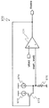
4a 1次巻線
4b 2次巻線
4c 補助巻線
5、14 整流ダイオード
6、15、102 平滑コンデンサ
7 出力状態検出回路
8 フォトカプラ
13、120、189、289、294、399、975 抵抗
100、200、400、900 スイッチング制御回路
101 スイッチング素子
110 フィードバック制御回路
110a I−Vコンバータ
111、115、117、119、175、192 N型MOSFET
112、114、191、397、973 P型MOSFET
113、116、173、190、193、396、398、972、974 定電流源118、122、172、187 基準電圧源
121 NPNバイポーラトランジスタ
140 パルス制御回路
150、450 電流検出回路
160 起動回路
170、270、970 間欠発振制御回路
174、290、295 コンデンサ
171、177、186 比較器
176 リセット回路
178、180、281、283 SH回路
179 初期値設定回路
181 遅延回路
182、282、288、292、293、298 インバータ回路
183、279、280、291、296 AND回路
184 RSフリップフロップ回路
185、285、385 間欠発振期間増減回路
188 オペアンプ
285a 立ち上がりエッジ検出回路
285b 立ち下がりエッジ検出回路
297、299 OR回路
430 変調回路
Claims (10)
- 直流の入力電圧が入力されるエネルギー変換回路と、
前記エネルギー変換回路から出力される電圧を整流平滑して負荷に出力電圧を出力する整流平滑回路と、
前記エネルギー変換回路に接続され、前記入力電圧をスイッチングするスイッチング素子と、
前記スイッチング素子のスイッチング動作を制御するスイッチング制御回路と、
前記出力電圧または前記負荷に流れる出力電流に応じたフィードバック信号を出力する出力状態検出回路とを有し、
前記スイッチング制御回路は、
前記出力電圧または前記出力電流が一定になるように前記フィードバック信号に応じて、前記スイッチング素子がスイッチング動作する発振期間とスイッチング動作が停止する停止期間とで構成されるサイクルが繰り返される間欠発振制御を行う間欠発振制御回路を備え、
前記間欠発振制御回路は、間欠発振制御の各サイクルにおいて、
前記発振期間と前記停止期間の和である間欠発振周期を予め設定されたターゲット周期と比較し、
前記間欠発振周期が前記ターゲット周期よりも短い場合には、
現在のサイクルの前記発振期間を前のサイクルの前記発振期間から第1の所定時間を延長した長さとし、
前記間欠発振周期が前記ターゲット周期よりも長い場合には、
現在のサイクルの前記発振期間を前のサイクルの前記発振期間から第2の所定時間を差し引いた長さとする
スイッチング電源装置。 - 前記間欠発振制御回路は、
現在のサイクルの前記発振期間の開始から充電または放電された容量素子の電圧と発振期間設定電圧とを比較して現在のサイクルの前記発振期間を設定する比較器とを有し、
前記発振期間設定電圧は、前のサイクルの前記発振期間完了時に記憶された前記容量素子の電圧値から前記第1の所定時間または前記第2の所定時間に対応する所定の電圧量を増減される
請求項1に記載のスイッチング電源装置。 - 前記第1の所定時間または前記第2の所定時間は
前記スイッチング素子のスイッチング動作周期の1/2倍から2倍の範囲で設定される
請求項1または2に記載のスイッチング電源装置。 - 前記第1の所定時間または前記第2の所定時間は
前記スイッチング素子のスイッチング動作回数の計数量により設定される
請求項1に記載のスイッチング電源装置。 - 前記計数量は1である
請求項4に記載のスイッチング電源装置。 - 前記間欠発振制御回路は、
前記間欠発振周期を第1の周期から第2の周期までの範囲で周期的に変化させる間欠発振周期変調手段を備えた
請求項1に記載のスイッチング電源装置。 - 前記間欠発振周期変調手段は、
前記ターゲット周期を予め設定された第3の周期から第4の周期までの範囲で周期的に変化させる
請求項6に記載のスイッチング電源装置。 - 前記間欠発振周期変調手段は、前記間欠発振周期が前記ターゲット周期に到達する毎に前記ターゲット周期を変更し、
前記ターゲット周期は、前記第3の周期および前記第4の周期のうちの一方に交互に変更される
請求項7に記載のスイッチング電源装置。 - 前記間欠発振周期変調手段は、
前記スイッチング素子を流れる電流ピーク値を設定するためのしきい値を予め設定された第1のしきい値から第2のしきい値までの範囲で周期的に変化させる
請求項6に記載のスイッチング電源装置。 - 請求項1から請求項9までのうちいずれか1つに記載のスイッチング電源装置において、
前記スイッチング制御回路を、半導体基板上に集積回路として形成した
スイッチング制御用の半導体装置。
Applications Claiming Priority (3)
| Application Number | Priority Date | Filing Date | Title |
|---|---|---|---|
| JP2016168485 | 2016-08-30 | ||
| JP2016168485 | 2016-08-30 | ||
| PCT/JP2017/030031 WO2018043227A1 (ja) | 2016-08-30 | 2017-08-23 | スイッチング電源装置および半導体装置 |
Publications (2)
| Publication Number | Publication Date |
|---|---|
| JPWO2018043227A1 JPWO2018043227A1 (ja) | 2019-06-24 |
| JP6810150B2 true JP6810150B2 (ja) | 2021-01-06 |
Family
ID=61300906
Family Applications (1)
| Application Number | Title | Priority Date | Filing Date |
|---|---|---|---|
| JP2018537171A Active JP6810150B2 (ja) | 2016-08-30 | 2017-08-23 | スイッチング電源装置および半導体装置 |
Country Status (3)
| Country | Link |
|---|---|
| US (1) | US10630186B2 (ja) |
| JP (1) | JP6810150B2 (ja) |
| WO (1) | WO2018043227A1 (ja) |
Families Citing this family (1)
| Publication number | Priority date | Publication date | Assignee | Title |
|---|---|---|---|---|
| CN109742964A (zh) * | 2018-12-28 | 2019-05-10 | 成都芯源系统有限公司 | 具有输入功率限制的ac/dc变换器的控制电路和方法 |
Family Cites Families (17)
| Publication number | Priority date | Publication date | Assignee | Title |
|---|---|---|---|---|
| JP3610964B2 (ja) * | 2002-05-13 | 2005-01-19 | 松下電器産業株式会社 | スイッチング電源装置 |
| JP4277628B2 (ja) | 2003-08-28 | 2009-06-10 | 株式会社デンソー | 車両用スイッチング電源装置 |
| JP4039362B2 (ja) | 2003-11-28 | 2008-01-30 | サンケン電気株式会社 | 直流変換装置 |
| US7471530B2 (en) | 2006-10-04 | 2008-12-30 | Power Integrations, Inc. | Method and apparatus to reduce audio frequencies in a switching power supply |
| JP4979536B2 (ja) | 2007-10-15 | 2012-07-18 | パナソニック株式会社 | スイッチング電源装置 |
| JP5343341B2 (ja) | 2007-10-18 | 2013-11-13 | サンケン電気株式会社 | スイッチング電源装置 |
| JP5230181B2 (ja) * | 2007-12-07 | 2013-07-10 | パナソニック株式会社 | エネルギー伝達装置およびエネルギー伝達制御用半導体装置 |
| JP2010022121A (ja) * | 2008-07-10 | 2010-01-28 | Panasonic Corp | スイッチング電源装置、およびスイッチング電源用半導体装置 |
| JP2010288334A (ja) * | 2009-06-09 | 2010-12-24 | Panasonic Corp | スイッチング電源装置及び半導体装置 |
| JP2011004550A (ja) | 2009-06-19 | 2011-01-06 | Panasonic Corp | スイッチング電源装置および半導体装置 |
| EP2383873B1 (en) | 2010-04-28 | 2013-06-19 | Nxp B.V. | Burst mode controller and method |
| WO2011158282A1 (ja) | 2010-06-14 | 2011-12-22 | パナソニック株式会社 | スイッチング電源装置およびその制御用半導体装置 |
| JP5485390B2 (ja) * | 2010-06-15 | 2014-05-07 | パナソニック株式会社 | スイッチング電源装置および半導体装置 |
| JP5640830B2 (ja) | 2011-03-10 | 2014-12-17 | サンケン電気株式会社 | スイッチング電源装置 |
| JP5845452B2 (ja) * | 2011-04-14 | 2016-01-20 | パナソニックIpマネジメント株式会社 | 半導体装置及びスイッチング電源装置 |
| JP5899504B2 (ja) * | 2011-11-28 | 2016-04-06 | パナソニックIpマネジメント株式会社 | スイッチング電源装置および半導体装置 |
| CN109643957B (zh) * | 2016-08-30 | 2020-12-11 | 松下半导体解决方案株式会社 | 开关电源装置以及半导体装置 |
-
2017
- 2017-08-23 WO PCT/JP2017/030031 patent/WO2018043227A1/ja active Application Filing
- 2017-08-23 JP JP2018537171A patent/JP6810150B2/ja active Active
-
2019
- 2019-02-22 US US16/282,735 patent/US10630186B2/en active Active
Also Published As
| Publication number | Publication date |
|---|---|
| WO2018043227A1 (ja) | 2018-03-08 |
| JPWO2018043227A1 (ja) | 2019-06-24 |
| US10630186B2 (en) | 2020-04-21 |
| US20190190388A1 (en) | 2019-06-20 |
Similar Documents
| Publication | Publication Date | Title |
|---|---|---|
| US10630188B2 (en) | Switching power supply apparatus and semiconductor device | |
| JP5230181B2 (ja) | エネルギー伝達装置およびエネルギー伝達制御用半導体装置 | |
| JP4481879B2 (ja) | スイッチング電源装置 | |
| JP4210868B2 (ja) | スイッチング電源装置 | |
| JP5424442B2 (ja) | ダイオード導通デューティ・サイクルを調節する装置 | |
| CN107210676B (zh) | 电源控制用半导体装置 | |
| US20090201705A1 (en) | Energy converting apparatus, and semiconductor device and switching control method used therein | |
| US8587966B2 (en) | Switching power supply device | |
| JP5978575B2 (ja) | スイッチング電源装置の制御回路およびスイッチング電源装置 | |
| US20030026115A1 (en) | Switching-type DC-DC converter | |
| JP2007295761A (ja) | スイッチング電源装置 | |
| US10630187B2 (en) | Switching power supply device and semiconductor device | |
| JP2008312359A (ja) | スイッチング電源装置、並びにレギュレーション回路 | |
| US20180191255A1 (en) | Switching power supply device | |
| US9318961B2 (en) | Switching power-supply device | |
| JP2004040856A (ja) | スイッチング電源装置 | |
| JP2011087394A (ja) | スイッチング素子駆動用制御回路およびスイッチング電源装置 | |
| JP6810150B2 (ja) | スイッチング電源装置および半導体装置 | |
| TWI672894B (zh) | 電源控制器與相關之控制方法 | |
| JP2016140183A (ja) | 電源制御用半導体装置 | |
| JP5854031B2 (ja) | スイッチング電源装置 | |
| JP4387244B2 (ja) | スイッチング電源装置 | |
| JP2010057207A (ja) | スイッチング電源装置 | |
| JPH11289762A (ja) | Dc−dcコンバータ | |
| JP2013099006A (ja) | 半導体集積回路装置 |
Legal Events
| Date | Code | Title | Description |
|---|---|---|---|
| A711 | Notification of change in applicant |
Free format text: JAPANESE INTERMEDIATE CODE: A711 Effective date: 20200217 |
|
| A621 | Written request for application examination |
Free format text: JAPANESE INTERMEDIATE CODE: A621 Effective date: 20200310 |
|
| A711 | Notification of change in applicant |
Free format text: JAPANESE INTERMEDIATE CODE: A711 Effective date: 20200520 |
|
| TRDD | Decision of grant or rejection written | ||
| A01 | Written decision to grant a patent or to grant a registration (utility model) |
Free format text: JAPANESE INTERMEDIATE CODE: A01 Effective date: 20201201 |
|
| A61 | First payment of annual fees (during grant procedure) |
Free format text: JAPANESE INTERMEDIATE CODE: A61 Effective date: 20201210 |
|
| R150 | Certificate of patent or registration of utility model |
Ref document number: 6810150 Country of ref document: JP Free format text: JAPANESE INTERMEDIATE CODE: R150 |
|
| R250 | Receipt of annual fees |
Free format text: JAPANESE INTERMEDIATE CODE: R250 |