JP6810150B2 - Switching power supply and semiconductor device - Google Patents
Switching power supply and semiconductor device Download PDFInfo
- Publication number
- JP6810150B2 JP6810150B2 JP2018537171A JP2018537171A JP6810150B2 JP 6810150 B2 JP6810150 B2 JP 6810150B2 JP 2018537171 A JP2018537171 A JP 2018537171A JP 2018537171 A JP2018537171 A JP 2018537171A JP 6810150 B2 JP6810150 B2 JP 6810150B2
- Authority
- JP
- Japan
- Prior art keywords
- intermittent oscillation
- cycle
- circuit
- switching
- voltage
- Prior art date
- Legal status (The legal status is an assumption and is not a legal conclusion. Google has not performed a legal analysis and makes no representation as to the accuracy of the status listed.)
- Active
Links
- 239000004065 semiconductor Substances 0.000 title claims description 29
- 230000010355 oscillation Effects 0.000 claims description 439
- 238000001514 detection method Methods 0.000 claims description 24
- 238000009499 grossing Methods 0.000 claims description 17
- 238000006243 chemical reaction Methods 0.000 claims description 9
- 239000000758 substrate Substances 0.000 claims description 7
- 230000003247 decreasing effect Effects 0.000 claims description 4
- 230000004044 response Effects 0.000 claims description 3
- 230000007423 decrease Effects 0.000 description 54
- 239000003990 capacitor Substances 0.000 description 21
- 238000010586 diagram Methods 0.000 description 21
- 238000004804 winding Methods 0.000 description 18
- 238000003708 edge detection Methods 0.000 description 10
- 230000008859 change Effects 0.000 description 7
- 230000000737 periodic effect Effects 0.000 description 6
- 230000000630 rising effect Effects 0.000 description 6
- 238000007792 addition Methods 0.000 description 4
- 230000000052 comparative effect Effects 0.000 description 4
- 230000000694 effects Effects 0.000 description 4
- 238000005516 engineering process Methods 0.000 description 4
- 238000000034 method Methods 0.000 description 4
- 230000009467 reduction Effects 0.000 description 4
- 230000000087 stabilizing effect Effects 0.000 description 3
- 238000004364 calculation method Methods 0.000 description 2
- 239000003985 ceramic capacitor Substances 0.000 description 2
- 238000007796 conventional method Methods 0.000 description 2
- 238000004519 manufacturing process Methods 0.000 description 2
- 230000001360 synchronised effect Effects 0.000 description 2
- 230000003111 delayed effect Effects 0.000 description 1
- 239000006185 dispersion Substances 0.000 description 1
- 230000007274 generation of a signal involved in cell-cell signaling Effects 0.000 description 1
- 230000006872 improvement Effects 0.000 description 1
- 238000012986 modification Methods 0.000 description 1
- 230000004048 modification Effects 0.000 description 1
- 238000012544 monitoring process Methods 0.000 description 1
- 238000004904 shortening Methods 0.000 description 1
- 230000001960 triggered effect Effects 0.000 description 1
- 239000013585 weight reducing agent Substances 0.000 description 1
- 229910000859 α-Fe Inorganic materials 0.000 description 1
Images


Classifications
-
- H—ELECTRICITY
- H02—GENERATION; CONVERSION OR DISTRIBUTION OF ELECTRIC POWER
- H02M—APPARATUS FOR CONVERSION BETWEEN AC AND AC, BETWEEN AC AND DC, OR BETWEEN DC AND DC, AND FOR USE WITH MAINS OR SIMILAR POWER SUPPLY SYSTEMS; CONVERSION OF DC OR AC INPUT POWER INTO SURGE OUTPUT POWER; CONTROL OR REGULATION THEREOF
- H02M3/00—Conversion of dc power input into dc power output
- H02M3/22—Conversion of dc power input into dc power output with intermediate conversion into ac
- H02M3/24—Conversion of dc power input into dc power output with intermediate conversion into ac by static converters
- H02M3/28—Conversion of dc power input into dc power output with intermediate conversion into ac by static converters using discharge tubes with control electrode or semiconductor devices with control electrode to produce the intermediate ac
- H02M3/325—Conversion of dc power input into dc power output with intermediate conversion into ac by static converters using discharge tubes with control electrode or semiconductor devices with control electrode to produce the intermediate ac using devices of a triode or a transistor type requiring continuous application of a control signal
- H02M3/335—Conversion of dc power input into dc power output with intermediate conversion into ac by static converters using discharge tubes with control electrode or semiconductor devices with control electrode to produce the intermediate ac using devices of a triode or a transistor type requiring continuous application of a control signal using semiconductor devices only
- H02M3/33507—Conversion of dc power input into dc power output with intermediate conversion into ac by static converters using discharge tubes with control electrode or semiconductor devices with control electrode to produce the intermediate ac using devices of a triode or a transistor type requiring continuous application of a control signal using semiconductor devices only with automatic control of the output voltage or current, e.g. flyback converters
-
- H—ELECTRICITY
- H02—GENERATION; CONVERSION OR DISTRIBUTION OF ELECTRIC POWER
- H02M—APPARATUS FOR CONVERSION BETWEEN AC AND AC, BETWEEN AC AND DC, OR BETWEEN DC AND DC, AND FOR USE WITH MAINS OR SIMILAR POWER SUPPLY SYSTEMS; CONVERSION OF DC OR AC INPUT POWER INTO SURGE OUTPUT POWER; CONTROL OR REGULATION THEREOF
- H02M3/00—Conversion of dc power input into dc power output
- H02M3/22—Conversion of dc power input into dc power output with intermediate conversion into ac
- H02M3/24—Conversion of dc power input into dc power output with intermediate conversion into ac by static converters
- H02M3/28—Conversion of dc power input into dc power output with intermediate conversion into ac by static converters using discharge tubes with control electrode or semiconductor devices with control electrode to produce the intermediate ac
- H02M3/325—Conversion of dc power input into dc power output with intermediate conversion into ac by static converters using discharge tubes with control electrode or semiconductor devices with control electrode to produce the intermediate ac using devices of a triode or a transistor type requiring continuous application of a control signal
- H02M3/335—Conversion of dc power input into dc power output with intermediate conversion into ac by static converters using discharge tubes with control electrode or semiconductor devices with control electrode to produce the intermediate ac using devices of a triode or a transistor type requiring continuous application of a control signal using semiconductor devices only
- H02M3/33507—Conversion of dc power input into dc power output with intermediate conversion into ac by static converters using discharge tubes with control electrode or semiconductor devices with control electrode to produce the intermediate ac using devices of a triode or a transistor type requiring continuous application of a control signal using semiconductor devices only with automatic control of the output voltage or current, e.g. flyback converters
- H02M3/33523—Conversion of dc power input into dc power output with intermediate conversion into ac by static converters using discharge tubes with control electrode or semiconductor devices with control electrode to produce the intermediate ac using devices of a triode or a transistor type requiring continuous application of a control signal using semiconductor devices only with automatic control of the output voltage or current, e.g. flyback converters with galvanic isolation between input and output of both the power stage and the feedback loop
Description
本開示は、軽負荷時の電源効率を改善するために間欠発振制御を備えたスイッチング電源装置およびそれを構成する半導体装置に関する。 The present disclosure relates to a switching power supply device provided with intermittent oscillation control in order to improve power supply efficiency at a light load, and a semiconductor device constituting the switching power supply device.
家電製品や事務機器等の電子機器には、電力変換効率の向上や小型化などの目的から、スイッチング電源装置が広く用いられている。スイッチング電源装置は、半導体のスイッチング素子などによるスイッチング動作を利用して出力電圧などを制御し、負荷に電力を供給する。 Switching power supply devices are widely used in electronic devices such as home appliances and office equipment for the purpose of improving power conversion efficiency and miniaturization. The switching power supply device controls an output voltage or the like by utilizing a switching operation by a semiconductor switching element or the like, and supplies electric power to a load.
このようなスイッチング電源装置において、電子機器の動作待機時の消費電力削減のため、軽負荷時の電源効率の改善が強く要求されている。 In such a switching power supply device, there is a strong demand for improvement of power supply efficiency at light load in order to reduce power consumption during standby operation of electronic devices.
一般的に、軽負荷時におけるスイッチング電源装置のエネルギー損失は、スイッチング動作によるスイッチング損失が支配的である。軽負荷時の電源効率を改善するためのよく知られている技術として、間欠発振制御が挙げられる。 In general, the energy loss of a switching power supply device under a light load is dominated by the switching loss due to the switching operation. Intermittent oscillation control is a well-known technique for improving power efficiency at light loads.
間欠発振制御の間欠発振周波数は、スイッチング周波数よりも低くなるため、20kHz以下の可聴周波数領域となることが多い。その結果として、可聴雑音が発生することがある。 Since the intermittent oscillation frequency of the intermittent oscillation control is lower than the switching frequency, it is often in the audible frequency region of 20 kHz or less. As a result, audible noise may occur.
可聴雑音の対策としては、トランスを接着あるいは含侵するなどが挙げられる。しかし、トランスにて対策する場合はコストアップを招く。 Countermeasures against audible noise include adhering or impregnating a transformer. However, if measures are taken with a transformer, the cost will increase.
上記のような課題を改善する従来の技術として、例えば特許文献1に開示されているものがある。特許文献1に開示されたスイッチング電源装置は、所望の間欠発振周期となるように負荷に応じた所望の間欠発振期間を計算し、間欠発振期間を制御することで間欠発振周期が調整される。例えば、所望の間欠発振周期を1msと設定することで、間欠発振周波数は1kHzとなり、可聴雑音を抑制することができる。 As a conventional technique for improving the above problems, for example, there is one disclosed in
しかしながら、特許文献1に開示されるような従来のスイッチング電源装置では、間欠発振制御時に負荷変動が発生すると所望の間欠発振期間の計算結果も大きく変化し、制御が不安定になる可能性がある。さらに不安定な制御が繰り返されることによって可聴周波数領域の周波数成分が増え、可聴雑音が発生する可能性もある。特許文献1には、不安定な制御の対策としてフィルター回路の追加が開示されているが、制御の複雑化や回路規模の増大を招いてしまう。 However, in the conventional switching power supply device as disclosed in
本開示は、上記の課題を解決し、軽負荷時に間欠発振制御を行うスイッチング電源装置において、間欠発振制御時の負荷変動に起因する可聴雑音を効果的に低減し、しかも、回路規模の増大を抑制し、かつ、制御の複雑化を抑制することが可能なスイッチング電源装置および半導体装置を提供することを目的とする。 The present disclosure solves the above-mentioned problems, effectively reduces audible noise caused by load fluctuation during intermittent oscillation control in a switching power supply device that performs intermittent oscillation control at light load, and further increases the circuit scale. An object of the present invention is to provide a switching power supply device and a semiconductor device capable of suppressing and suppressing the complexity of control.
上記の課題を解決するために、本開示のスイッチング電源装置は、直流の入力電圧が入力されるエネルギー変換回路と、前記エネルギー変換回路から出力される電圧を整流平滑して負荷に出力電圧を出力する整流平滑回路と、前記エネルギー変換回路に接続され、前記入力電圧をスイッチングするスイッチング素子と、前記スイッチング素子のスイッチング動作を制御するスイッチング制御回路と、前記出力電圧または前記負荷に流れる出力電流に応じたフィードバック信号を出力する出力状態検出回路とを有し、前記スイッチング制御回路は、前記出力電圧または前記出力電流が一定になるように前記フィードバック信号に応じて、前記スイッチング素子がスイッチング動作する発振期間とスイッチング動作が停止する停止期間とで構成されるサイクルが繰り返される間欠発振制御を行う間欠発振制御回路を備え、前記間欠発振制御回路は、間欠発振制御の各サイクルにおいて、前記発振期間と前記停止期間の和である間欠発振周期を予め設定されたターゲット周期と比較し、前記間欠発振周期が前記ターゲット周期よりも短い場合には現在のサイクルの前記発振期間を前のサイクルの前記発振期間から第1の所定時間を延長した長さとし、前記間欠発振周期が前記ターゲット周期よりも長い場合には現在のサイクルの前記発振期間を前のサイクルの前記発振期間から第2の所定時間を差し引いた長さとする。 In order to solve the above problems, the switching power supply device of the present disclosure rectifies and smoothes an energy conversion circuit into which a DC input voltage is input and a voltage output from the energy conversion circuit, and outputs an output voltage to a load. An oscillating smoothing circuit, a switching element connected to the energy conversion circuit to switch the input voltage, a switching control circuit for controlling the switching operation of the switching element, and an output current flowing through the output voltage or the load. The switching control circuit has an output state detection circuit that outputs a feedback signal, and the switching control circuit has an oscillation period in which the switching element switches in response to the feedback signal so that the output voltage or the output current becomes constant. The intermittent oscillation control circuit is provided with an intermittent oscillation control circuit that repeats a cycle composed of a stop period and a stop period in which the switching operation is stopped. The intermittent oscillation control circuit is provided with the oscillation period and the stop in each cycle of the intermittent oscillation control. The intermittent oscillation cycle, which is the sum of the periods, is compared with the preset target cycle, and when the intermittent oscillation cycle is shorter than the target cycle, the oscillation period of the current cycle is changed from the oscillation period of the previous cycle. The length is an extension of the predetermined time of 1, and when the intermittent oscillation cycle is longer than the target cycle, the oscillation period of the current cycle is defined as the length obtained by subtracting the second predetermined time from the oscillation period of the previous cycle. To do.
本開示に係るスイッチング電源装置によれば、間欠発振周期を間欠発振周期ターゲット値と比較した結果に基づいて間欠発振期間を制御することで可聴雑音を抑制することができる。さらに、間欠発振制御時の負荷変動に対しても、間欠発振期間の変化量は予め設定された量の増減だけであり、制御安定のための回路の追加などは不要である。 According to the switching power supply device according to the present disclosure, audible noise can be suppressed by controlling the intermittent oscillation period based on the result of comparing the intermittent oscillation cycle with the intermittent oscillation cycle target value. Further, with respect to the load fluctuation during the intermittent oscillation control, the amount of change in the intermittent oscillation period is only an increase or decrease of a preset amount, and it is not necessary to add a circuit for stabilizing the control.
また、前記間欠発振制御回路は、現在のサイクルの前記発振期間の開始から充電または放電された容量素子の電圧と発振期間設定電圧とを比較して現在のサイクルの前記発振期間を設定する比較器を有し、前記発振期間設定電圧は、前のサイクルの前記発振期間完了時に記憶された前記容量素子の電圧値から前記第1の所定時間または前記第2の所定時間に対応する所定の電圧量を増減されてもよい。 Further, the intermittent oscillation control circuit is a comparator that sets the oscillation period of the current cycle by comparing the voltage of the capacitive element charged or discharged from the start of the oscillation period of the current cycle with the oscillation period setting voltage. The oscillation period set voltage is a predetermined voltage amount corresponding to the first predetermined time or the second predetermined time from the voltage value of the capacitive element stored at the completion of the oscillation period in the previous cycle. May be increased or decreased.
本開示に係るスイッチング電源装置によれば、簡素な回路で間欠発振制御が実現できる。 According to the switching power supply device according to the present disclosure, intermittent oscillation control can be realized with a simple circuit.
また、前記第1の所定時間または前記第2の所定時間は前記スイッチング素子のスイッチング動作周期の1/2倍から2倍の範囲で設定されてもよい。 Further, the first predetermined time or the second predetermined time may be set in the range of 1/2 to 2 times the switching operation cycle of the switching element.
本開示に係るスイッチング電源装置によれば、第1の所定時間または第2の所定時間がスイッチング素子のスイッチング動作1回分相当となり、より安定した間欠発振制御が可能となる。 According to the switching power supply device according to the present disclosure, the first predetermined time or the second predetermined time corresponds to one switching operation of the switching element, and more stable intermittent oscillation control becomes possible.
また、前記第1の所定時間または前記第2の所定時間は前記スイッチング素子のスイッチング動作回数の計数量により設定されてもよい。 Further, the first predetermined time or the second predetermined time may be set by the counting amount of the number of switching operations of the switching element.
本開示に係るスイッチング電源装置によれば、第1の所定時間または第2の所定時間の設定に対して製造ばらつきを考慮不要にできる。 According to the switching power supply device according to the present disclosure, it is possible to eliminate the need to consider manufacturing variations with respect to the setting of the first predetermined time or the second predetermined time.
また、前記計数量は1であってもよい。 Further, the counting amount may be 1.
本開示に係るスイッチング電源装置によれば第1の所定時間または第2の所定時間がスイッチング素子のスイッチング動作1回分相当となり、より安定した間欠発振制御が可能となる。 According to the switching power supply device according to the present disclosure, the first predetermined time or the second predetermined time corresponds to one switching operation of the switching element, and more stable intermittent oscillation control becomes possible.
また、前記間欠発振制御回路は、前記間欠発振周期を第1の周期から第2の周期までの範囲で周期的に変化させる間欠発振周期変調手段を備えてもよい。 Further, the intermittent oscillation control circuit may include an intermittent oscillation cycle modulation means that periodically changes the intermittent oscillation cycle in the range from the first cycle to the second cycle.
本開示に係るスイッチング電源装置によれば、間欠発振周波数を分散させることができ可聴雑音の抑制効果を高めることができる。 According to the switching power supply device according to the present disclosure, the intermittent oscillation frequency can be dispersed and the effect of suppressing audible noise can be enhanced.
また、前記間欠発振周期変調手段は、前記ターゲット周期を予め設定された第3の周期から第4の周期までの範囲で周期的に変化させてもよい。 Further, the intermittent oscillation period modulation means may periodically change the target period in a preset range from a third period to a fourth period.
本開示に係るスイッチング電源装置によれば、効果的に間欠発振周波数を分散させることができる。 According to the switching power supply device according to the present disclosure, the intermittent oscillation frequency can be effectively dispersed.
また、前記間欠発振周期変調手段は、前記間欠発振周期が前記ターゲット周期に到達する毎に前記ターゲット周期を変更し、前記ターゲット周期は、前記第3の周期および前記第4の周期のうちの一方に交互に変更されてもよい。 Further, the intermittent oscillation cycle modulation means changes the target cycle each time the intermittent oscillation cycle reaches the target cycle, and the target cycle is one of the third cycle and the fourth cycle. May be changed alternately.
本開示に係るスイッチング電源装置によれば、簡素な回路で間欠発振周波数の分散が可能となる。 According to the switching power supply device according to the present disclosure, it is possible to disperse the intermittent oscillation frequency with a simple circuit.
また、前記間欠発振周期変調手段は、前記スイッチング素子を流れる電流ピーク値を設定するためのしきい値を予め設定された第1のしきい値から第2のしきい値までの範囲で周期的に変化させてもよい。 Further, the intermittent oscillation periodic modulation means periodically sets a threshold value for setting the current peak value flowing through the switching element in a range from a preset first threshold value to a second threshold value. May be changed to.
本開示に係るスイッチング電源装置によれば、間欠発振制御の各サイクルにおける供給エネルギーの離散性が改善され、間欠発振周波数を分散することができる。 According to the switching power supply device according to the present disclosure, the discreteness of the supply energy in each cycle of the intermittent oscillation control is improved, and the intermittent oscillation frequency can be dispersed.
また、前記スイッチング制御回路を、半導体基板上に集積回路として形成した半導体装置であってもよい。 Further, the switching control circuit may be a semiconductor device formed as an integrated circuit on a semiconductor substrate.
本開示に係る半導体装置によれば、スイッチング電源装置の部品点数を大幅に削減することができ、小型化および軽量化さらには低コスト化を容易に実現することができる。 According to the semiconductor device according to the present disclosure, the number of parts of the switching power supply device can be significantly reduced, and it is possible to easily realize miniaturization, weight reduction, and cost reduction.
以上のように本開示によれば、間欠発振制御時にトランスやセラミックコンデンサなどの部品から発生する可聴雑音を効果的に低減することができ、さらに、負荷変動が発生しても制御が不安定にならないスイッチング電源装置を比較的簡素な回路構成で実現できる。 As described above, according to the present disclosure, it is possible to effectively reduce audible noise generated from parts such as a transformer and a ceramic capacitor during intermittent oscillation control, and further, the control becomes unstable even if load fluctuations occur. It is possible to realize a switching power supply device with a relatively simple circuit configuration.
(本開示の基礎となった知見)
本発明者らは、「背景技術」の欄において記載したスイッチング電源装置に関し、以下の問題が生じることを見出した。(Knowledge on which this disclosure was based)
The present inventors have found that the following problems occur with respect to the switching power supply device described in the “Background Art” column.
図14は、比較参照例におけるスイッチング電源装置の一例を示す回路図である。図14に示すスイッチング電源装置は、スイッチング制御回路900内部に図15に示す間欠発振制御回路970を有している。間欠発振制御回路970は、FB端子電流に応じて変化する制御信号VEAOを利用して、軽負荷状態を検出し、間欠発振期間と間欠停止期間を繰り返す間欠発振制御を行う。 FIG. 14 is a circuit diagram showing an example of a switching power supply device in the comparative reference example. The switching power supply device shown in FIG. 14 has an intermittent
図16は、図14のスイッチング電源装置において、間欠発振制御時の各動作波形を示すタイミングチャートである。間欠発振制御回路970は、制御信号VEAOとヒステリシスを有する基準電圧(ここではVref1とVref2の2つ)とを比較することで間欠発振制御信号Enableを生成する。間欠発振制御信号Enableのハイレベル期間を間欠発振期間Tonとし、ローレベル期間を間欠停止期間Toffとする。こうして、間欠発振制御回路970は、間欠発振期間Tonと間欠停止期間Toffとからなる間欠発振周期Tonoffを繰り返す間欠発振制御を実現している。負荷が軽くなればなるほど、間欠停止期間Toffが長くなり、一定期間あたりのスイッチング回数が削減されることで電源効率が改善される。なお、通常動作中は電流モードのPWM制御を、例えば、25kHzのスイッチング周波数で実行しているものとすると、間欠発振期間Ton内のスイッチング周波数も25kHzでスイッチング動作する。 FIG. 16 is a timing chart showing each operation waveform during intermittent oscillation control in the switching power supply device of FIG. The intermittent
このような動作において、間欠発振期間Tonと間欠停止期間Toffからなる間欠発振制御の間欠発振周波数(間欠発振周期Tonoffの逆数)は、スイッチング周波数よりも低くなるため、20kHz以下の可聴周波数領域となることが多い。その結果として、スイッチング電源装置において使用されるトランスやコンデンサから音鳴りが発生する場合がある。特に、一般に使用されるフェライトコアのトランスの場合、5kHzから15kHzの範囲において、機械的な共振により電子機器には望ましくない可聴雑音が発生することがある。 In such an operation, the intermittent oscillation frequency (the reciprocal of the intermittent oscillation cycle Tonoff) of the intermittent oscillation control consisting of the intermittent oscillation period Ton and the intermittent stop period Toff is lower than the switching frequency, so that the audible frequency region is 20 kHz or less. Often. As a result, noise may be generated from transformers and capacitors used in switching power supply devices. In particular, in the case of a commonly used ferrite core transformer, undesired audible noise may be generated in an electronic device due to mechanical resonance in the range of 5 kHz to 15 kHz.
可聴雑音の対策としては、トランスを接着あるいは含侵するなどが挙げられる。しかし、トランスにて対策する場合はコストアップを招く。 Countermeasures against audible noise include adhering or impregnating a transformer. However, if measures are taken with a transformer, the cost will increase.
可聴雑音を改善する従来の技術として、例えば特許文献1に開示されているものがある。特許文献1に開示されたスイッチング電源装置は、所望の間欠発振周期となるように負荷に応じた所望の間欠発振期間を計算し、間欠発振期間を制御することで間欠発振周期が調整される。例えば、所望の間欠発振周期を1msと設定することで、間欠発振周波数は1kHzとなり、可聴雑音を抑制することができる。 As a conventional technique for improving audible noise, for example, there is one disclosed in
しかしながら、特許文献1に開示されるようなスイッチング電源装置では、間欠発振制御時に負荷変動が発生すると所望の間欠発振期間の計算結果も大きく変化し、制御が不安定になる可能性がある。 However, in a switching power supply device as disclosed in
さらに不安定な制御が繰り返されることによって可聴周波数領域の周波数成分が増え、可聴雑音が発生する可能性もある。 Further, repeated unstable control increases the frequency component in the audible frequency region, which may cause audible noise.
特許文献1には、不安定な制御の対策としてフィルター回路の追加が開示されているが、制御の複雑化や回路規模の増大を招いてしまう。
そこで、本開示は、上記の課題を解決し、軽負荷時に間欠発振制御を行うスイッチング電源装置において、間欠発振制御時の負荷変動に起因する可聴雑音を効果的に低減し、しかも、回路規模の増大を抑制し、かつ、制御の複雑化を抑制することが可能なスイッチング電源装置および半導体装置を提供する。 Therefore, the present disclosure solves the above-mentioned problems, effectively reduces audible noise caused by load fluctuation during intermittent oscillation control in a switching power supply device that performs intermittent oscillation control at light load, and further, the circuit scale. Provided are a switching power supply device and a semiconductor device capable of suppressing an increase and suppressing complicated control.
以下、本開示のスイッチング電源装置および半導体装置について図面を参照しながら説明する。但し、詳細な説明は省略する場合がある。例えば、既によく知られた事項の詳細説明や実質的に同一の構成に対する重複説明を省略する場合がある。これは、以下の説明が不必要に冗長になるのを避け、当業者の理解を容易にするためである。 Hereinafter, the switching power supply device and the semiconductor device of the present disclosure will be described with reference to the drawings. However, detailed description may be omitted. For example, detailed explanations of already well-known matters and duplicate explanations for substantially the same configuration may be omitted. This is to avoid unnecessary redundancy of the following description and to facilitate the understanding of those skilled in the art.
なお、添付図面および以下の説明は当業者が本開示を十分に理解するためのものであって、これらによって請求の範囲に記載の主題を限定することを意図するものではない。 It should be noted that the accompanying drawings and the following description are for those skilled in the art to fully understand the present disclosure, and are not intended to limit the subject matter described in the claims.
(実施の形態1)
以下、実施の形態1に係るスイッチング電源装置および半導体装置について、図1〜5を参照しながら具体的に説明する。(Embodiment 1)
Hereinafter, the switching power supply device and the semiconductor device according to the first embodiment will be specifically described with reference to FIGS. 1 to 5.
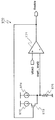
図1は、本実施の形態1のスイッチング制御用半導体装置を備えたスイッチング電源装置の一構成を示す回路図である。 FIG. 1 is a circuit diagram showing a configuration of a switching power supply device including the semiconductor device for switching control according to the first embodiment.
図1において、スイッチング電源装置は、トランス4、整流ダイオード5、平滑コンデンサ6、出力状態検出回路7、フォトカプラ8、抵抗13、整流ダイオード14、平滑コンデンサ15およびスイッチング制御回路100を備える。 In FIG. 1, the switching power supply device includes a
トランス4は1次巻線4a、2次巻線4b、および補助巻線4cを有したエネルギー変換回路であり、1次巻線4aと2次巻線4bの極性は逆になっている。このスイッチング電源装置はフライバック型である。 The
1次巻線4aには、スイッチング電源装置の入力端子の高電位側と、スイッチング制御回路100の一部を構成するスイッチング素子101が接続されている。スイッチング素子101の駆動電極(ゲート)に印加する電圧信号を変化させることにより、スイッチング素子101のスイッチング動作が制御される。 A switching
2次巻線4bには整流ダイオード5と平滑コンデンサ6とで構成された整流平滑回路が接続されており、スイッチング動作によって2次巻線4bに発生するフライバック電圧が、整流平滑されて出力電圧Voutが生成される。 A rectifying and smoothing circuit composed of a rectifying
スイッチング素子101を含むスイッチング制御回路100は、半導体基板上に形成され、スイッチング制御用の1つの半導体装置を構成している。このスイッチング素子101は、パワーMOSFETなどから構成されている。 The switching
なお、スイッチング制御回路100において、スイッチング素子101を除く部分とスイッチング素子101とは同一の半導体基板上に設けられてもよいし、別の半導体基板上に設けられてもよい。例えば、スイッチング制御回路100におけるスイッチング素子101を除く部分が配置された一方の半導体基板に、当該部分から駆動信号を出力するための出力端子を設け、他方の半導体基板上に配置されたスイッチング素子101のゲートに接続するようにしてもよい。また、スイッチング素子101とスイッチング素子101を除く部分を2つ以上の半導体装置として分離して構成してもよい。 In the
スイッチング制御回路100は、外部入出力端子として、DRAIN端子、VCC端子、FB端子、IS端子、およびGND端子の5つの端子を有している。また、例えば、スイッチング制御回路100は、スイッチング素子101、平滑コンデンサ102、フィードバック制御回路110、パルス制御回路140、電流検出回路150、起動回路160、間欠発振制御回路170などから構成される。 The switching
DRAIN端子は、トランス4の1次巻線4aとスイッチング素子101の接続点、すなわちスイッチング素子101のドレインに接続される端子である。 The DRAIN terminal is a terminal connected to the connection point between the primary winding 4a of the
VCC端子は、トランス4の補助巻線4cに接続された整流ダイオード14と平滑コンデンサ15とで構成される整流平滑回路の出力と、スイッチング制御回路100に内蔵された起動回路160を接続する端子であり、スイッチング素子101のスイッチング動作により補助巻線4cに発生するフライバック電圧を整流平滑し、制御電源電圧VCCとしてスイッチング制御回路100に電力供給する端子である。 The VCS terminal is a terminal for connecting the output of the rectifying and smoothing circuit composed of the rectifying
FB端子は、出力状態検出回路7から出力されるフィードバック信号(例えば、フォトカプラ8による電流など)をスイッチング制御回路100のフィードバック制御回路110に入力するための端子である。 The FB terminal is a terminal for inputting a feedback signal (for example, a current due to the photocoupler 8) output from the output state detection circuit 7 to the
IS端子は、スイッチング素子101および電流検出回路150と、抵抗13を接続する端子であり、スイッチング素子101を流れる電流を検出するための端子である。 The IS terminal is a terminal for connecting the
GND端子は、スイッチング制御回路100の電位基準であるGNDをスイッチング電源装置の入力端子の低電位側に接続する端子である。 The GND terminal is a terminal that connects the GND, which is the potential reference of the switching
起動回路160は、DRAIN端子、VCC端子、平滑コンデンサ102およびスイッチング制御回路100の回路内部電圧源VDDに接続されている。スイッチング電源装置の起動時には、入力直流電圧Vinがトランス4の1次巻線4aを介してDRAIN端子に印加されると、DRAIN端子から起動回路160を介して、平滑コンデンサ102および15に起動電流が流れる。平滑コンデンサ102および15が充電され、VDD電圧およびVCC端子電圧が上昇し、それぞれ起動電圧に達すると、起動回路160は起動電流をカットする。また、起動回路160は、スイッチング素子101のスイッチング動作可否を判断するためVCC端子電圧をモニターしており、図には示していないが、パルス制御回路140などに起動・停止信号を出力している。 The
パルス制御回路140は、スイッチング素子101のスイッチング動作を制御するための回路であり、電流検出回路150、間欠発振制御回路170から入力される信号などからスイッチング動作や停止、ターンオンタイミングやターンオフタイミングを決定する。なお、パルス制御回路140には、ターンオンタイミングのための周期的なクロック信号を発生させる発振器などのターンオン信号生成回路やスイッチング素子101を駆動するためのドライブ回路などが含まれる。発振器のクロック信号は例えば、25kHzの周波数に設定される。 The
電流検出回路150は、スイッチング素子101を流れる電流を検出するため、IS端子に接続された抵抗13に発生する電圧信号が入力され、あらかじめ設定された基準電圧と比較し、スイッチング素子101をターンオフさせるためのターンオフ信号をパルス制御回路140に出力する。なお、比較するための基準電圧は、スイッチング制御方式によってはフィードバック制御回路110からの制御信号VEAOに応じて変化してもよい。例えば、通常動作中は電流モードのPWM制御を行う場合、制御信号VEAOに応じて、負荷が重くなるほど基準電圧を上昇させる。また、間欠発振制御時は基準電圧を一定とすることでスイッチング素子101を流れる電流ピーク値を一定としてもよい。 In order to detect the current flowing through the switching
フィードバック制御回路110は、出力状態検出回路7から出力されるフィードバック信号がFB端子を介して入力され、スイッチング素子101のスイッチング動作を制御するための制御信号VEAOを生成する。例えば、通常動作中は電流モードのPWM制御を行う場合、スイッチング素子101を流れる電流を制御するため、制御信号VEAOを電流検出回路150へ出力する。また、負荷に応じた間欠発振制御を行うため、間欠発振制御回路170にも制御信号VEAOを出力する。 The
図2は、本実施の形態1のフィードバック制御回路110の一構成を示す回路図である。フィードバック制御回路110は、定電流源113、116と、P型MOSFET112、114と、N型MOSFET111、115、117、119と、基準電圧源118、122と、抵抗120およびNPNバイポーラトランジスタ121から構成される。N型MOSFET119、抵抗120、NPNバイポーラトランジスタ121および基準電圧源122は、I−Vコンバータ110aを構成し、FB端子電流に比例した電流を電圧信号に変換し、制御信号VEAOを生成する。FB端子から流出する電流が大きいほど制御信号VEAOが低下し、それに伴いスイッチング素子101に流れる電流ピーク値は低く制御される。 FIG. 2 is a circuit diagram showing a configuration of the
間欠発振制御回路170は、フィードバック制御回路110から入力された制御信号VEAOに応じて、間欠発振制御を行うための間欠発振制御信号Enableをパルス制御回路140に出力する。パルス制御回路140は、間欠発振制御信号Enableがハイレベルの期間を間欠発振期間として、スイッチング素子101のスイッチング動作を制御する。また、パルス制御回路140は、間欠発振制御信号Enableがローレベルの期間を間欠停止期間として、スイッチング素子101のスイッチング動作を停止することで間欠発振制御を行う。 The intermittent
図3は、本実施の形態1の間欠発振制御回路170の一構成例を示す回路図である。間欠発振制御回路170は、比較器171、177と、基準電圧源172と、定電流源173と、コンデンサ174と、N型MOSFET175と、リセット回路176と、SH(SHはサンプル&ホールドの略)回路178、180と、初期値設定回路179と、遅延回路181と、インバータ回路182と、AND回路183と、RSフリップフロップ回路184および間欠発振期間増減回路185から構成される。制御信号VEAOが基準電圧源172による基準電圧Vrefと比較され、制御信号VEAOが基準電圧Vrefよりも高くなるとRSフリップフロップ回路184のセット(S)入力端子にハイレベルが入力され、間欠発振制御信号Enableがハイレベルとなり、スイッチング素子101のスイッチング動作が可能となる。一方、RSフリップフロップ回路184のリセット(R)入力端子には、AND回路183の出力端子が接続されており、そのAND回路183には、比較器171の出力がインバータ回路182によって反転された信号と比較器177の出力信号とが入力されている。比較器177は、ランプ電圧Vrampと間欠発振期間設定電圧Vonを比較し、比較器171の出力が既にローレベルに反転している時には間欠発振期間Tonの完了タイミングを決定する。ランプ電圧Vrampが間欠発振期間設定電圧Vonよりも大きくなり、間欠発振期間Tonの完了タイミングとなると、RSフリップフロップ回路184のリセット(R)端子にハイレベルの信号が入力され、間欠発振制御信号Enableがローレベルとなることで、スイッチング素子101のスイッチング動作が停止する。その後、再び制御信号VEAOが基準電圧Vrefよりも高くなると、間欠発振制御信号Enableがハイレベルとなることで、間欠停止期間Toffが完了し、スイッチング素子101のスイッチング動作が再開される。このように、間欠発振期間Tonと間欠停止期間Toffとで構成されたサイクルが繰り返され、間欠発振制御が行われる。なお、ランプ電圧Vrampは、コンデンサ174を定電流源173の定電流によって充電することで生成され、間欠発振周期の各サイクルにおいて、間欠発振期間Tonの開始からの経過時間のモニターに使用される。また、間欠発振期間設定電圧Vonは、間欠発振周期の各サイクルにおいて、前の間欠発振期間設定電圧VonNとSH回路178から出力された間欠発振周期信号Vonoffが間欠発振期間増減回路185に入力され、SH回路180および初期値設定回路179を介して設定される。FIG. 3 is a circuit diagram showing a configuration example of the intermittent
図4は、本実施の形態1の間欠発振期間増減回路185の一構成例を示す回路図である。間欠発振期間増減回路185は、比較器186と、基準電圧源187と、オペアンプ188と、抵抗189と、定電流源190、193と、P型MOSFET191およびN型MOSFET192から構成される。SH回路178から入力された間欠発振周期信号Vonoffを基準電圧源187による間欠発振周期ターゲット電圧Vtargetと比較し、抵抗189に流れる定電流の向きを切り替える。SH回路180によって保持されている前のサイクルの間欠発振期間設定電圧VonNが入力され、オペアンプ188によりインピーダンス変換された後、定電流源190による定電流値と抵抗189の抵抗値の積(第1の電圧降下値Vd1とも呼ぶ)が加算、または定電流源193による定電流値と抵抗189の抵抗値の積(第2の電圧降下値Vd2とも呼ぶ)が減算されることで現在のサイクルの間欠発振期間設定電圧VonN+1が生成される。FIG. 4 is a circuit diagram showing a configuration example of the intermittent oscillation period increase /
言い換えれば、比較器186は、間欠発振期間Tonと間欠停止期間Toffとの和である間欠発振周期Tonoffを、予め設定されたターゲット周期(Vtargetで定まる時間)と比較する。比較の結果、間欠発振周期Tonoffがターゲット周期(Vtargetで定まる時間)よりも短い場合には、間欠発振期間増減回路185は、現在のサイクルの間欠発振期間(VonN+1で定まる時間)を前のサイクルの発振期間(VonNで定まる時間)から第1の所定時間(つまり第1の電圧降下値Vd1に対応する時間)を延長した長さとする。この場合、例えば、VonN+1は、VonNに第1の電圧降下値Vd1を加算した電圧である。In other words, the
一方、比較の結果、間欠発振周期Tonoffがターゲット周期(Vtargetで定まる時間)よりも長い場合には、間欠発振期間増減回路185は、現在のサイクルの発振期間(VonN+1で定まる時間)を前のサイクルの前記発振期間(VonNで定まる時間)から第2の所定時間(つまり第2の電圧降下値Vd2に対応する時間)を差し引いた長さとする。この場合、例えば、VonN+1は、VonNから第2の電圧降下値Vd2を差し引いた電圧である。On the other hand, as a result of comparison, when the intermittent oscillation cycle Tonoff is longer than the target period (time determined by Vtaget), the intermittent oscillation period increase /
また、出力状態検出回路7は、検出抵抗、ツェナーダイオード、シャントレギュレータなどで構成され、出力電圧Voutの電圧レベルを検出し、その出力電圧Voutが所定の電圧に安定するように、フォトカプラ8を介してフィードバック信号をスイッチング制御回路100に出力する。なお、出力電圧Voutの検出には、補助巻線4cに発生するフライバック電圧を利用してもよく、整流ダイオード14および平滑コンデンサ15による整流平滑後のVCC電圧を利用してもよい。 Further, the output state detection circuit 7 is composed of a detection resistor, a Zener diode, a shunt regulator, etc., detects the voltage level of the output voltage Vout, and sets the
以上のように構成された図1に示すスイッチング電源装置およびスイッチング制御用半導体装置の動作を説明する。 The operation of the switching power supply device and the semiconductor device for switching control shown in FIG. 1 configured as described above will be described.
商用電源などの交流電圧が、ブリッジダイオードや平滑コンデンサなどにより整流平滑され、入力直流電圧Vinが生成される。この入力直流電圧Vinは、トランス4の1次巻線4aを介して、スイッチング制御回路100のDRAIN端子に印加され、DRAIN端子から起動回路160を介して、VCC端子に接続されている平滑コンデンサ15に起動電流が流れる。VCC端子電圧が上昇し、起動回路160で設定された起動電圧に達すると、スイッチング素子101のスイッチング制御が開始される。 The AC voltage of a commercial power supply or the like is rectified and smoothed by a bridge diode or a smoothing capacitor, and an input DC voltage Vin is generated. This input DC voltage Vin is applied to the DRAIN terminal of the switching
一旦、スイッチング素子101がターンオンすると、スイッチング素子101および抵抗13に電流が流れ、電流の大きさに応じた電圧信号が電流検出回路150に入力される。あらかじめ設定された基準電圧以上に上昇すると、スイッチング素子101はターンオフする。 Once the switching
スイッチング素子101がターンオフすると、スイッチング素子101のオン時間中にトランス4の1次側に電流が流れることによって蓄えられたエネルギーが2次側に伝達される。 When the
以上のようなスイッチング動作が繰り返されて、出力電圧Voutが上昇していくが、出力状態検出回路7で設定された所定の電圧以上になると、出力状態検出回路7およびフォトカプラ8は、フィードバック信号としてスイッチング制御回路100のFB端子から電流を流出するよう制御する。この流出電流の大きさで、フィードバック制御回路110は、スイッチング素子101を流れる電流または一定期間あたりのスイッチング回数を調整する。 The above switching operation is repeated, and the output voltage Vout rises. However, when the voltage exceeds the predetermined voltage set by the output state detection circuit 7, the output state detection circuit 7 and the
具体的には、スイッチング電源装置に接続される負荷への電流供給が大きい重負荷時にはスイッチング素子101を流れる電流を高く設定し、軽負荷時にはスイッチング素子101を流れる電流を低く設定する。さらに負荷が軽くなると間欠発振制御を行うことでスイッチング回数を低減する。このように、スイッチング制御回路100は、スイッチング電源装置に接続される負荷に供給される電力に応じて、スイッチング素子101のスイッチング動作を変化させながら、出力電圧Voutを所定の電圧に安定させるように制御を行う。 Specifically, when the current supply to the load connected to the switching power supply device is large, the current flowing through the switching
ここで、間欠発振制御回路170の動作について説明する。負荷が軽くなり、FB端子電流が増加すると、制御信号VEAOが基準電圧源172による基準電圧Vrefよりも低下し、比較器171の出力がローレベルとなる。インバータ回路182からAND回路183にハイレベルが入力される。一方、それまでの発振期間が十分長ければ定電流源173とコンデンサ174で生成されるランプ電圧Vrampは十分に上昇しており、間欠発振期間設定電圧Vonよりも高いため、比較器177の出力もハイレベルとなっている。その結果、RSフリップフロップ回路184のリセット(R)にAND回路183からハイレベルが入力され、間欠発振制御信号Enableがローレベルとなる。よって、スイッチング素子101のスイッチング動作が停止し、間欠発振期間Tonが完了する。 Here, the operation of the intermittent
スイッチング動作が停止すると出力電圧Voutが低下し、FB端子電流が減少する。制御信号VEAOが基準電圧Vrefよりも上昇すると、比較器171の出力がハイレベルに反転し、RSフリップフロップ回路184のセット(S)に入力され、間欠発振制御信号Enableがハイレベルに反転する。間欠発振制御信号Enableがハイレベルになると、スイッチング素子101のスイッチング動作が再開されると同時に、SH回路178、リセット回路176および遅延回路181が動作するトリガーとなる。まず、SH回路178がランプ電圧Vrampをサンプリングし、間欠発振周期信号Vonoffとして記憶し、間欠発振期間増減回路185へ出力する。さらに、間欠発振期間増減回路185は初期値設定回路179から前のサイクルの間欠発振期間TonNに相当する電圧VonNが入力されており、現在のサイクルの間欠発振期間TonN+1に相当する電圧VonN+1を生成し、SH回路180に出力する。When the switching operation is stopped, the output voltage Vout drops and the FB terminal current decreases. When the control signal VEAO rises above the reference voltage Vref, the output of the
一方、遅延回路181は、間欠発振制御信号Enableがハイレベルに反転してから遅延時間を設けて、SH回路180を動作させる。遅延時間は、間欠発振制御信号Enableがハイレベルに反転してからSH回路178が動作し、間欠発振期間増減回路185の出力が安定するまでに必要な時間であればよく、例えば、1μs程度に設定される。SH回路180は、間欠発振期間増減回路185の出力をサンプリングし、初期値設定回路179へ出力する。初期値設定回路179は、スイッチング電源装置の起動時などにSH回路180から出力がない場合に初期値を設定するものであり、SH回路180に前のサイクルの間欠発振期間増減回路185の出力が記憶されていれば、そのまま、SH回路180からの出力を間欠発振期間設定電圧Vonとして比較器177の基準側(−)へ出力する。なお、初期値設定回路179で設定される初期値は、予め設定された固定値でもよいし、スイッチング電源装置の起動後の最初のサイクルの間欠発振期間Ton0を元に設定されてもよい。On the other hand, the
ここで、比較器177の検出側(+)に入力されるランプ電圧Vrampについて説明する。ランプ電圧Vrampは、定電流源173による定電流によってコンデンサ174が充電されることで生成され、リセット回路176によって制御される。 Here, the lamp voltage Vram input to the detection side (+) of the
リセット回路176は、間欠発振制御信号EnableがハイレベルになるとN型MOSFET175を導通し、コンデンサ174に蓄積された電荷を放電し、ランプ電圧Vrampをリセットする。なお、SH回路178がランプ電圧Vrampをサンプリングし記憶する時間を考慮し、間欠発振制御信号EnableがハイレベルになってからN型MOSFET175の導通までに遅延時間を設けてもよいが、間欠発振期間Tonよりも十分に短い必要がある。 When the intermittent oscillation control signal Enable becomes high level, the
ランプ電圧Vrampのリセットが完了するとN型MOSFET175は非導通とされ、ランプ電圧Vrampは再び上昇を始める。すなわち、ランプ電圧Vrampは間欠発振制御の各サイクルの開始からの経過時間に比例し、間欠発振期間Tonや間欠発振周期Tonoffのモニター信号として使用できる。 When the reset of the lamp voltage Vram is completed, the N-
間欠発振期間Tonのモニター信号として使用されるランプ電圧Vrampは、前述の間欠発振期間設定電圧Vonと比較器177で比較される。ランプ電圧Vrampが間欠発振期間設定電圧Vonよりも高くなると、比較器177の出力はハイレベルに反転し、AND回路183に入力される。制御信号VEAOが基準電圧Vrefよりも低下し、インバータ回路182の出力がハイレベルとなっている場合には、AND回路183の出力がハイレベルに反転し、RSフリップフロップ回路184がリセットされ、間欠発振制御信号Enableがローレベルに反転され、間欠発振期間Tonが完了する。よって、間欠発振制御の各サイクルにおいて、間欠発振期間設定電圧Vonの制御により間欠発振期間が変化し、間欠発振周期Tonoffおよび間欠発振周波数が調整される。 The lamp voltage Vram used as a monitor signal for the intermittent oscillation period Ton is compared with the above-mentioned intermittent oscillation period set voltage Von by the
間欠発振期間設定電圧Vonの制御は、間欠発振期間増減回路185によって電圧値を決定し、遅延回路181およびSH回路180によって電圧値変更し記憶するタイミングを調整することで行われる。なお、初期値設定回路179によって初期値が設定される。 The intermittent oscillation period setting voltage Von is controlled by determining the voltage value by the intermittent oscillation period increase /
間欠発振期間増減回路185は、前のサイクルの間欠発振周期信号Vonoffと間欠発振周期ターゲット電圧Vtargetを比較し、周期判定信号Judgeを生成する。間欠発振周期ターゲット電圧Vtargetは、ランプ電圧Vrampの上昇速度を考慮して設定され、例えば、間欠発振周期ターゲット値1ms(間欠発振周波数ターゲット値1kHz)に相当する電圧に設定される。 The intermittent oscillation period increase /
前のサイクルの間欠発振周期TonoffNが間欠発振周期ターゲット値よりも短い場合には、周期判定信号Judgeはローレベルとなり、P型MOSFET191が導通し、定電流源190による定電流が抵抗189およびオペアンプ188に流れる。この結果、現在のサイクルの間欠発振期間設定電圧VonN+1は、前のサイクルの間欠発振期間設定電圧VonNに定電流源190による定電流値と抵抗189の抵抗値の積(第1の電圧降下値Vd1)が加算された電圧値となる。すなわち、現在のサイクルの発振期間(VonN+1で定まるTon)は、前のサイクルの発振期間(VonNで定まるTon)から第1の所定時間(第1の電圧降下値Vd1に対応する時間)を延長した長さになる。なお、定電流源190による定電流値と抵抗189の抵抗値の積(つまり第1の電圧降下値Vd1)は、スイッチング素子101のスイッチング動作周期1周期に相当する電圧値が好ましい。スイッチング素子101のスイッチング周波数が25kHzの場合、例えば、スイッチング動作周期の1/2倍から2倍の範囲となるように20μsから80μsの範囲に相当する電圧値に設定するとよい。When the intermittent oscillation cycle Tonoff N of the previous cycle is shorter than the intermittent oscillation cycle target value, the cycle determination signal Judge becomes low level, the P-
一方、前のサイクルの間欠発振周期TonoffNが間欠発振周期ターゲット値よりも長い場合には、周期判定信号Judgeはハイレベルとなり、N型MOSFET192が導通し、定電流源193による定電流が抵抗189およびオペアンプ188に流れる。この結果、現在のサイクルの間欠発振期間設定電圧VonN+1は、前のサイクルの間欠発振期間設定電圧VonNから定電流源190による定電流値と抵抗189の抵抗値の積(つまり第2の電圧降下値Vd2)が減算された電圧値となる。すなわち、現在のサイクルの発振期間(VonN+1で定まるTon)は、前のサイクルの発振期間(VonNで定まるTon)から第2の所定時間(第2の電圧降下値Vd2に対応する時間)を差し引いた長さとなる。On the other hand, when the intermittent oscillation cycle Tonoff N of the previous cycle is longer than the intermittent oscillation cycle target value, the cycle determination signal Judge becomes high level, the N-
以上より、現在のサイクルの間欠発振期間TonN+1を前のサイクルの間欠発振期間TonNから所定時間、例えば、スイッチング素子101のスイッチング動作周期1周期分だけ延長または短縮し、間欠発振周期Tonoffを間欠発振周期ターゲット値に近づける制御となる。間欠発振周期Tonoffが間欠発振周期ターゲット値に到達するまで上記間欠発振制御サイクルを繰り返すことで、間欠発振周波数を所望の周波数に制御することができる。From the above, the intermittent oscillation period Ton N + 1 of the current cycle is extended or shortened from the intermittent oscillation period Ton N of the previous cycle by a predetermined time, for example, one switching operation cycle of the
なお、第1の所定時間は、スイッチング素子101のスイッチング動作周期の1/2倍から2倍の範囲内の時間であってもよい。また、第2の所定時間は、スイッチング素子101のスイッチング動作周期の1/2倍から2倍の範囲内の時間であってもよい。 The first predetermined time may be a time within the range of 1/2 to 2 times the switching operation cycle of the
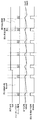
次に、図5に示すタイミングチャートを用いて、本実施の形態1におけるスイッチング電源装置の間欠発振制御の一動作例を説明する。図5には、スイッチング電源装置から供給される負荷電流Iout、スイッチング素子101を流れるドレイン電流、制御信号VEAO、間欠発振制御信号Enable、ランプ電圧Vramp、間欠発振周期信号Vonoff、周期判定信号Judgeおよび間欠発振期間設定電圧Vonが示されている。また、図5は、スイッチング電源装置から供給される負荷電流Ioutが変化したときの間欠発振制御の動作例である。 Next, an operation example of intermittent oscillation control of the switching power supply device according to the first embodiment will be described with reference to the timing chart shown in FIG. In FIG. 5, the load current Iout supplied from the switching power supply device, the drain current flowing through the switching
負荷電流Ioutが小さい期間は、間欠発振周期Tonoffが間欠発振周期ターゲット値となるように間欠発振期間Tonが制御され、スイッチング素子101のスイッチング回数が2回または3回で安定している。なお、スイッチング素子101のスイッチング動作による供給エネルギーはスイッチング回数に応じて離散的となるため、間欠発振周期Tonoffが間欠発振周期ターゲット値に一致しない場合は、例えば、スイッチング回数が2回または3回を交互に繰り返すように、間欠発振期間Tonが変化していても安定しているとみなす。 During the period when the load current Iout is small, the intermittent oscillation period Ton is controlled so that the intermittent oscillation cycle Tonoff becomes the intermittent oscillation cycle target value, and the switching frequency of the
負荷電流Ioutが大きくなると、スイッチング回数が2回または3回では間欠発振周期Tonoffが間欠発振周期ターゲット値に対して短くなり、周期判定信号Judgeはローレベルで維持される。そのため、間欠発振期間増減回路185は、間欠発振期間設定電圧Vonを、定電流源190による定電流値と抵抗189の抵抗値によって予め設定された量だけ増やし続け、間欠発振期間Tonが徐々に延長されていく。それに伴い、間欠発振期間Tonの間のスイッチング素子101のスイッチング回数も3回、4回、5回と増加していき、6回となるサイクルでようやく間欠発振周期Tonoffが間欠発振周期ターゲット値に到達する。その後、間欠発振期間Tonの間のスイッチング素子101のスイッチング回数は5回または6回で安定する。 When the load current Iout becomes large, the intermittent oscillation cycle Tonoff becomes shorter than the intermittent oscillation cycle target value when the number of switching times is 2 or 3, and the cycle determination signal Judge is maintained at a low level. Therefore, the intermittent oscillation period increase /
このようにして、負荷電流Ioutが変化しても、間欠発振周期Tonoffが間欠発振周期ターゲット値となるように間欠発振期間Tonが制御され、また間欠発振期間Tonは、定電流源190による定電流値と抵抗189の抵抗値によって予め設定された量の増減を繰り返すことで調整される。 In this way, even if the load current Iout changes, the intermittent oscillation period Ton is controlled so that the intermittent oscillation cycle Tonoff becomes the intermittent oscillation cycle target value, and the intermittent oscillation period Ton is a constant current generated by the constant
以上より、本実施の形態1のスイッチング電源装置は、間欠発振周期Tonoffを間欠発振周期ターゲット値と比較した結果に基づいて間欠発振期間Tonを制御することで、負荷に応じて間欠発振周期Tonoffを調整できる。間欠発振周期Tonoffの調整を繰り返すことで間欠発振周波数を間欠発振周波数ターゲット値に近づけることができ、例えば1kHzに設定することで可聴雑音を抑制することができる。 From the above, the switching power supply device of the first embodiment controls the intermittent oscillation period Tonoff based on the result of comparing the intermittent oscillation cycle Tonoff with the intermittent oscillation cycle target value, thereby setting the intermittent oscillation cycle Tonoff according to the load. Can be adjusted. By repeating the adjustment of the intermittent oscillation cycle Tonoff, the intermittent oscillation frequency can be brought closer to the intermittent oscillation frequency target value. For example, by setting it to 1 kHz, audible noise can be suppressed.
さらに、間欠発振制御時の負荷変動に対しても、間欠発振期間Tonの変化量は予め設定された量の増減だけであり、制御安定のための回路の追加などは不要である。また、間欠発振期間Tonを制御する間欠発振期間増減回路185は、比較器186と予め設定された量を増減する回路だけで構成され、非常に簡素な回路で実現することができる。 Further, with respect to the load fluctuation during the intermittent oscillation control, the amount of change in the intermittent oscillation period Ton is only an increase or decrease of a preset amount, and it is not necessary to add a circuit for stabilizing the control. Further, the intermittent oscillation period increase /
なお、間欠発振期間増減回路185は、間欠発振周期Tonoffと間欠発振周期ターゲット値を比較しているが、間欠発振周波数をモニターし、間欠発振周波数ターゲット値と比較するようにしてもよい。また、間欠発振周期Tonoffのモニターはランプ電圧Vrampを使用しているが、カウント回路を用いてクロック信号Clockを計数することで代替してもよい。 Although the intermittent oscillation period increase /
また、間欠発振期間Tonの延長または短縮は、間欠発振期間設定電圧Vonの変更ではなく、ランプ電圧Vrampの変更で行ってもよい。例えば、リセット回路176によるリセット時間を長くして充電開始タイミングを遅らせることで間欠発振期間Tonを延長したり、リセット回路176によるリセットを不十分にして充電開始時のランプ電圧Vrampを高くすることで間欠発振期間Tonを短縮してもよい。 Further, the intermittent oscillation period Ton may be extended or shortened by changing the lamp voltage Vramp instead of changing the intermittent oscillation period setting voltage Von. For example, the reset time by the
また、間欠発振期間増減回路185の定電流源190と193の定電流値は同じでなくともよい。 Further, the constant current values of the constant
また、間欠発振制御回路170のコンデンサ174をスイッチング制御回路100に外付けされたコンデンサを使用してもよい。 Further, the
また、間欠発振周期ターゲット電圧Vtargetや間欠発振期間Tonを変化させる所定の量をスイッチング制御回路100に外付けされた回路部品で調整できるようにしてもよい。 Further, a predetermined amount for changing the intermittent oscillation cycle target voltage Vtarget and the intermittent oscillation period Ton may be adjusted by a circuit component externally attached to the switching
また、パルス制御回路140は、クロック信号が固定周波数であるPWM制御、可変周波数であるPFM制御、共振動作を利用した擬似共振制御や電流共振制御など、様々な制御形態を適用してもよい。 Further, the
また、負荷状態を示すフィードバック信号を生成するため、出力状態検出回路7とフォトカプラ8を設けているが、2次側の出力電圧Voutから検出するのではなく、補助巻線4cまたは整流平滑後のVCC端子電圧から検出し、フィードバック信号を生成してもよい。 Further, in order to generate a feedback signal indicating a load state, an output state detection circuit 7 and a
また、出力状態検出回路7は、2次側出力電圧Voutを一定にするようなフィードバック信号を生成する定電圧制御ではなく、負荷電流Ioutを一定にするようなフィードバック信号を生成する定電流制御でもよい。 Further, the output state detection circuit 7 is not a constant voltage control that generates a feedback signal that makes the secondary output voltage Vout constant, but a constant current control that generates a feedback signal that makes the load current Iout constant. Good.
また、フライバック型のスイッチング電源装置の構成について説明したが、フォワード型や降圧チョッパー型などトポロジーが異なる構成でもよい。 Further, although the configuration of the flyback type switching power supply device has been described, a configuration having a different topology such as a forward type or a step-down chopper type may be used.
(実施の形態2)
次に、実施の形態2に係るスイッチング電源装置および半導体装置について、図6〜9を参照しながら説明する。(Embodiment 2)
Next, the switching power supply device and the semiconductor device according to the second embodiment will be described with reference to FIGS. 6 to 9.
実施の形態1では、間欠発振制御の各サイクルにおいて、前のサイクルの間欠発振周期信号Vonoffと間欠発振周期ターゲット電圧Vtargetを比較した結果に基づいて間欠発振期間設定電圧Vonを制御していた。本実施の形態2では、前のサイクルの間欠発振周期信号Vonoffと間欠発振周期ターゲット電圧Vtargetを比較した結果に基づいて、パルス制御回路140で生成されるクロック信号Clockの1周期分を前のサイクルの間欠発振期間TonNから延長または短縮する間欠発振制御回路270を備えたスイッチング電源装置について説明する。なお、実施の形態1と重複する説明は省略する。In the first embodiment, in each cycle of the intermittent oscillation control, the intermittent oscillation period setting voltage Von is controlled based on the result of comparing the intermittent oscillation cycle signal Vonoff and the intermittent oscillation cycle target voltage Vtarget of the previous cycle. In the second embodiment, one cycle of the clock signal Clock generated by the
図6は、本実施の形態2のスイッチング電源装置の一構成例を示す回路図である。同図のスイッチング電源装置は、実施の形態1のスイッチング電源装置を示す図1と比較して、スイッチング制御回路100の代わりにスイッチング制御回路200を備える点が異なる。以下、異なる点を中心に説明する。スイッチング制御回路200は、図1のスイッチング制御回路100と比較して、間欠発振制御回路170の代わりに間欠発振制御回路270を備える点が異なる。また、図7は、本実施の形態2のスイッチング電源装置の間欠発振制御回路270の一構成例を示す回路図である。実施の形態1の間欠発振制御回路170を示す図3と比較して、SH回路178、初期値設定回路179、SH回路180、遅延回路181、AND回路183および間欠発振期間増減回路185が削除された点と、パルス制御回路140からクロック信号Clockが入力される点と、AND回路279、280と、インバータ回路282と、SH(SHはサンプル&ホールドの略)回路281、283および間欠発振期間増減回路285が追加されている点とが異なる。また、図8は、本実施の形態2のスイッチング電源装置の間欠発振期間増減回路285の一構成例を示す回路図である。実施の形態1の間欠発振期間増減回路185を示す図4と比較して、オペアンプ188と、抵抗189と、定電流源190、193と、P型MOSFET191およびN型MOSFET192が削除された点と、クロック信号Clockが入力される点と、立ち上がりエッジ検出回路285aと、立ち下がりエッジ検出回路285bと、OR回路297、299およびインバータ回路298が追加された点とが異なっている。なお、立ち上がりエッジ検出回路285aは、インバータ回路288と、抵抗289と、コンデンサ290およびAND回路291で構成されている。立ち下がりエッジ検出回路285bは、インバータ回路292、293と、抵抗294と、コンデンサ295およびAND回路296で構成されている。 FIG. 6 is a circuit diagram showing a configuration example of the switching power supply device according to the second embodiment. The switching power supply device of the figure is different from FIG. 1 showing the switching power supply device of the first embodiment in that it includes a switching
以上のように構成された本実施の形態2に係るスイッチング電源装置および半導体装置の動作について、実施の形態1と異なる間欠発振制御を中心に説明する。 The operation of the switching power supply device and the semiconductor device according to the second embodiment configured as described above will be described focusing on the intermittent oscillation control different from that of the first embodiment.
軽負荷時の間欠発振制御は、実施の形態1と同様に、RSフリップフロップ回路184の出力である間欠発振制御信号Enableによって、スイッチング素子101のスイッチング動作を制御する。一方、間欠発振期間増減回路285の出力信号である間欠発振期間増加信号Upおよび間欠発振期間減少信号DownがRSフリップフロップ回路184のセットまたはリセットタイミングを変更することで、間欠発振期間Tonを制御する。 In the intermittent oscillation control at the time of light load, the switching operation of the
間欠発振期間設定電圧Vonは、インバータ回路282およびSH回路281によって前のサイクルの間欠発振期間TonNに相当する電圧VonNに設定される。よって、ランプ電圧Vrampと間欠発振期間設定電圧Vonを比較する比較器177は、間欠発振制御の各サイクルにおいて、前のサイクルの間欠発振期間TonNと同等の時間が経過するとハイレベルに反転することになる。インバータ回路182の出力および間欠発振期間増加信号Upがハイレベルである場合は、比較器177の出力がハイレベルに反転するタイミングでAND回路280を介してRSフリップフロップ回路184がリセットされ、間欠発振期間Tonが完了する。間欠発振期間増加信号Upがローレベルの場合は、間欠発振期間増加信号Upがハイレベルに反転するまで間欠発振期間Tonが延長されることになる。The intermittent oscillation period setting voltage Von is set to a voltage Von N corresponding to the intermittent oscillation period Ton N of the previous cycle by the
スイッチング素子101のスイッチング動作が停止すると出力電圧Voutが低下し、FB端子電流が減少する。制御信号VEAOが基準電圧Vrefを上回ると、比較器171の出力がハイレベルに反転する。間欠発振期間減少信号Downがハイレベルである場合は、比較器171の出力がハイレベルに反転するタイミングでAND回路279を介してRSフリップフロップ回路184がセットされ、間欠発振期間Tonが開始される。間欠発振期間減少信号Downがローレベルの場合は、間欠発振期間減少信号Downがハイレベルに反転するまで間欠発振期間Tonの開始が遅れる。すなわち、現在のサイクルの間欠発振期間TonN+1が前のサイクルの間欠発振期間TonNから所定の時間だけ短縮されることになる。When the switching operation of the
以上のように、間欠発振期間増加信号Upによって前のサイクルの間欠発振期間TonNから所定時間だけ延長される、または、間欠発振期間減少信号Downによって前のサイクルの間欠発振期間TonNから所定時間だけ短縮されることによって、間欠発振期間Tonが制御される。As described above, the intermittent oscillation period increase signal Up extends the intermittent oscillation period Ton N of the previous cycle by a predetermined time, or the intermittent oscillation period decrease signal Down extends the intermittent oscillation period Ton N of the previous cycle by a predetermined time. By shortening, the intermittent oscillation period Ton is controlled.
間欠発振期間増加信号Upおよび間欠発振期間減少信号Downは、間欠発振期間増減回路285によって生成される。間欠発振期間増減回路285には、パルス制御回路140からのクロック信号ClockとSH回路283の出力である間欠発振周期信号Vonoffが入力される。SH回路283は、比較器171の出力がハイレベルに反転するタイミングで、ランプ電圧Vrampをサンプリングおよび記憶して、間欠発振周期信号Vonoffを生成する。 The intermittent oscillation period increase signal Up and the intermittent oscillation period decrease signal Down are generated by the intermittent oscillation period increase /
間欠発振期間増減回路285は、前のサイクルの間欠発振周期に相当する間欠発振周期信号Vonoffと間欠発振周期ターゲット電圧Vtargetを比較し、周期判定信号Judgeを生成する。 The intermittent oscillation period increase /
前のサイクルの間欠発振周期TonoffNが間欠発振周期ターゲット値よりも短い場合には、周期判定信号Judgeはローレベルとなり、間欠発振期間減少信号Downはハイレベルに固定される。また、間欠発振期間増加信号Upは、クロック信号Clockが入力された立ち上がりエッジ検出回路285aの出力に依存される。間欠発振期間増加信号Upは、クロック信号Clockがローレベルからハイレベルに反転するタイミングで立ち上がり、立ち上がりエッジ検出回路285aで設定される幅のパルス状の信号であり、クロック信号Clockに同期している。よって、間欠発振制御回路270のAND回路280には、比較器177の出力がハイレベルになった後、次のクロック信号Clockのパルスが立ち上がるタイミングで間欠発振期間増加信号Upのハイレベルが入力される。間欠発振期間増加信号Upのハイレベルの入力によってRSフリップフロップ回路184がリセットされ、間欠発振制御信号Enableがローレベルに反転する。すなわち、前のサイクルの間欠発振期間TonNにスイッチング素子101のスイッチング動作1回分の時間が追加されてから、現在のサイクルの間欠発振期間TonN+1が完了する。When the intermittent oscillation cycle Tonoff N of the previous cycle is shorter than the intermittent oscillation cycle target value, the cycle determination signal Judge becomes a low level, and the intermittent oscillation period decrease signal Down is fixed at a high level. Further, the intermittent oscillation period increase signal Up depends on the output of the rising
一方、前のサイクルの間欠発振周期TonoffNが間欠発振周期ターゲット値よりも長い場合には、周期判定信号Judgeはハイレベルとなり、間欠発振期間増加信号Upはハイレベルに固定される。また、間欠発振期間減少信号Downは、クロック信号Clockが入力された立ち下がりエッジ検出回路285bの出力に依存する。間欠発振期間減少信号Downは、クロック信号Clockがハイレベルからローレベルに反転するタイミングで立ち上がり、立ち下がりエッジ検出回路285bで設定される幅のパルス状の信号であり、クロック信号Clockに同期している。よって、間欠発振制御回路270のAND回路279には、比較器171の出力がハイレベルになった後、次のクロック信号Clockがハイレベルからローレベルに反転するタイミングで間欠発振期間減少信号Downのハイレベルが入力される。すなわち、比較器171の出力がハイレベルに反転し、次のクロック信号Clockのパルス信号が立ち下がってからRSフリップフロップ回路184がセットされる。そのため、実質、前のサイクルの間欠停止期間ToffNが延長され、現在のサイクルの間欠発振期間TonN+1は前のサイクルの間欠発振期間TonNからスイッチング素子101のスイッチング動作1回分の時間が短縮されることになる。On the other hand, when the intermittent oscillation cycle Tonoff N of the previous cycle is longer than the intermittent oscillation cycle target value, the cycle determination signal Judge becomes a high level, and the intermittent oscillation period increase signal Up is fixed at a high level. Further, the intermittent oscillation period reduction signal Down depends on the output of the falling
図9は、本実施の形態2におけるスイッチング電源装置の間欠発振制御の一動作例を示すタイミングチャートである。実施の形態1を示す図5と比較して、間欠発振期間増加信号Upと間欠発振期間減少信号Downが追加されている。 FIG. 9 is a timing chart showing an operation example of intermittent oscillation control of the switching power supply device according to the second embodiment. An intermittent oscillation period increase signal Up and an intermittent oscillation period decrease signal Down are added as compared with FIG. 5 showing the first embodiment.
実施の形態1と同様に、負荷電流Ioutが変化しても、間欠発振周期Tonoffが間欠発振周期ターゲット値となるように間欠発振期間Tonが制御され、また間欠発振期間Tonは、パルス制御回路140のクロック信号Clockの1周期分、すなわち、スイッチング素子101のスイッチング動作1回分といった予め設定された量の増減を繰り返すことで調整される。 Similar to the first embodiment, even if the load current Iout changes, the intermittent oscillation period Ton is controlled so that the intermittent oscillation cycle Tonoff becomes the intermittent oscillation cycle target value, and the intermittent oscillation period Ton is the
以上より、本実施の形態2のスイッチング電源装置は、実施の形態1と同様に、間欠発振周期Tonoffを間欠発振周期ターゲット値と比較した結果に基づいて間欠発振期間Tonを制御することで、負荷に応じて間欠発振周期Tonoffを調整できる。 From the above, the switching power supply device of the second embodiment is loaded by controlling the intermittent oscillation period Ton based on the result of comparing the intermittent oscillation cycle Tonoff with the intermittent oscillation cycle target value, as in the first embodiment. The intermittent oscillation cycle Tonoff can be adjusted according to the above.
さらに、間欠発振制御時の負荷変動に対しても、間欠発振期間Tonの変化量は予め設定された量の増減だけであり、制御安定のための回路の追加などは不要である。また、間欠発振期間Tonを制御する間欠発振期間増減回路285は、比較器186とRSフリップフロップ回路184のセットまたはリセットのタイミングを変更する回路だけで構成され、非常に簡素な回路で実現することができる。 Further, with respect to the load fluctuation during the intermittent oscillation control, the amount of change in the intermittent oscillation period Ton is only an increase or decrease of a preset amount, and it is not necessary to add a circuit for stabilizing the control. Further, the intermittent oscillation period increase /
さらに、間欠発振期間Tonを増減するための予め設定された量は、パルス制御回路140のクロック信号Clockの周期で設定され、製造ばらつきなどを考慮する必要がなくなる。 Further, the preset amount for increasing or decreasing the intermittent oscillation period Ton is set in the cycle of the clock signal Clock of the
なお、間欠発振期間Tonを増減するための予め設定された量は、パルス制御回路140のクロック信号Clockの1周期を利用しているが、複数周期をカウントして利用してもよい。 Although one cycle of the clock signal Clock of the
また、間欠発振周期Tonoffのモニターはランプ電圧Vrampを使用しているが、カウント回路を用いてクロック信号Clockを計数することで代替してもよい。 Further, although the monitor of the intermittent oscillation cycle Tonoff uses the lamp voltage voltage, it may be replaced by counting the clock signal Clock using the counting circuit.
(実施の形態3)
次に、実施の形態3に係るスイッチング電源装置および半導体装置について、図10および11を参照しながら説明する。(Embodiment 3)
Next, the switching power supply device and the semiconductor device according to the third embodiment will be described with reference to FIGS. 10 and 11.
実施の形態1では、間欠発振周期ターゲット電圧Vtargetは固定値に設定されていたが、本実施の形態3では、間欠発振周期ターゲット電圧Vtargetが周期的に変化するスイッチング電源装置について説明する。なお、実施の形態1と重複する説明は省略する。 In the first embodiment, the intermittent oscillation cycle target voltage Vtaget is set to a fixed value, but in the third embodiment, a switching power supply device in which the intermittent oscillation cycle target voltage Vtaget changes periodically will be described. The description overlapping with the first embodiment will be omitted.
図10は、本実施の形態3のスイッチング電源装置の間欠発振期間増減回路385の一構成例を示す回路図である。同図の間欠発振期間増減回路385は、実施の形態1の間欠発振期間増減回路185を示す図4と比較して、基準電圧源187の代わりに、定電流源396、398と、P型MOSFET397および抵抗399を備える点が異なっている。 FIG. 10 is a circuit diagram showing a configuration example of the intermittent oscillation period increase /
以上のように構成された本実施の形態3に係るスイッチング電源装置および半導体装置の動作について、実施の形態1と異なる間欠発振期間の増減制御を中心に説明する。 The operation of the switching power supply device and the semiconductor device according to the third embodiment configured as described above will be described focusing on the increase / decrease control of the intermittent oscillation period different from that of the first embodiment.
比較器186の基準側(−)の間欠発振周期ターゲット電圧Vtargetは、周期判定信号Judgeがハイレベルの時には、定電流源398の定電流値と抵抗399の抵抗値の積で設定され、周期判定信号Judgeがローレベルの時には、P型MOSFET397が導通して定電流源396の定電流値と抵抗399の抵抗値の積の分だけ上昇する。すなわち、間欠発振周期ターゲット電圧Vtargetは、第1の間欠発振周期ターゲット電圧Vtarget1と定電流源396の定電流値と抵抗399の抵抗値の積の分だけ高い第2の間欠発振周期ターゲット電圧Vtarget2を周期判定信号Judgeに応じて周期的に切り替えられる。 The intermittent oscillation period target voltage voltage Vtaget on the reference side (-) of the
図11は、本実施の形態3におけるスイッチング電源装置の間欠発振制御の一動作例を示すタイミングチャートである。図11には、スイッチング素子101を流れるドレイン電流、間欠発振周期ターゲット電圧Vtarget、間欠発振周期Tonoffおよび間欠発振周波数が示されている。なお、スイッチング素子101を流れるドレイン電流は、間欠発振期間Tonの波形を長方形のブロックで示している。例えば、“20回”と表記されたブロックは、間欠発振期間Tonの間にスイッチング素子101のスイッチング動作が20回含まれることを示す。なお、図11は、スイッチング電源装置から供給される負荷電流Ioutが一定のときの間欠発振制御の動作例である。 FIG. 11 is a timing chart showing an operation example of intermittent oscillation control of the switching power supply device according to the third embodiment. FIG. 11 shows the drain current flowing through the switching
実施の形態1と同様に、間欠発振周期Tonoffが間欠発振周期ターゲット値となるように間欠発振期間Tonが制御されるが、本実施の形態3では、間欠発振周期ターゲット電圧Vtargetが、周期判定信号Judgeに応じて周期的に変化する。そのため、負荷電流Ioutが一定でも、間欠発振周期ターゲット電圧Vtargetの変化に応じて第1の間欠発振周期ターゲット値Ttarget1から第2の間欠発振周期ターゲット値Ttarget2の範囲で間欠発振周期Tonoffは周期的に変化し、間欠発振周期Tonoffの逆数である間欠発振周波数も第2の間欠発振周波数ターゲット値Ftarget2から第1の間欠発振周波数ターゲット値Ftarget1の範囲で周期的に変化する。 Similar to the first embodiment, the intermittent oscillation period Ton is controlled so that the intermittent oscillation cycle Tonoff becomes the intermittent oscillation cycle target value. However, in the third embodiment, the intermittent oscillation cycle target voltage Vtaget is a cycle determination signal. It changes periodically according to the Judge. Therefore, even if the load current Iout is constant, the intermittent oscillation cycle Tonoff periodically falls within the range of the first intermittent oscillation cycle target value Target1 to the second intermittent oscillation cycle target value Target2 according to the change in the intermittent oscillation cycle target voltage Vtaget. The intermittent oscillation frequency, which is the inverse of the intermittent oscillation period Tonoff, also changes periodically in the range from the second intermittent oscillation frequency target value Ftarget2 to the first intermittent oscillation frequency target value Ftarget1.
以上より、本実施の形態3のスイッチング電源装置は、実施の形態1と同等の効果を得ることができ、さらに、間欠発振周期Tonoffを周期的に変調することで間欠発振周波数を分散することができる。間欠発振周波数の分散によって特定周波数へのエネルギー集中を緩和し、可聴雑音の抑制効果を高めることができる。 From the above, the switching power supply device of the third embodiment can obtain the same effect as that of the first embodiment, and further, the intermittent oscillation frequency can be dispersed by periodically modulating the intermittent oscillation cycle Tonoff. it can. By dispersing the intermittent oscillation frequency, energy concentration on a specific frequency can be relaxed and the effect of suppressing audible noise can be enhanced.
なお、間欠発振周波数の分散度合いを大きくするため、周期判定信号Judgeのハイレベルまたはローレベルは間欠発振制御の2サイクル以上で維持されることが望ましく、第1の間欠発振周期ターゲット電圧Vtarget1と第2の間欠発振周期ターゲット電圧Vtarget2の差で設定が可能である。 In order to increase the degree of dispersion of the intermittent oscillation frequency, it is desirable that the high level or low level of the period determination signal Judge is maintained in two or more cycles of intermittent oscillation control, and the first intermittent oscillation period target voltage Vtaget1 and the first It can be set by the difference of the intermittent oscillation cycle target voltage Vtaget2 of 2.
なお、間欠発振周期ターゲット電圧Vtargetを周期判定信号Judgeに応じて周期的に切り替えているが、周期判定信号Judgeに関係なく変調してもよい。例えば、間欠発振期間増減回路385の定電流源396、398およびP型MOSFET397を削除し、代わりに、周期的に変調された電流を抵抗399に流すことで、周期的に変化する間欠発振周期ターゲット電圧Vtargetを生成してもよい。この場合、電流の変調周期は、間欠発振周期Tonoffに対して十分に長い方がよい。 Although the intermittent oscillation cycle target voltage Vtaget is periodically switched according to the cycle determination signal Judge, it may be modulated regardless of the cycle determination signal Judge. For example, by deleting the constant
(実施の形態4)
次に、実施の形態4に係るスイッチング電源装置および半導体装置について、図12および13を参照しながら説明する。(Embodiment 4)
Next, the switching power supply device and the semiconductor device according to the fourth embodiment will be described with reference to FIGS. 12 and 13.
実施の形態3では、間欠発振周期ターゲット電圧Vtargetを周期的に変化させることで間欠発振周波数を分散させたが、本実施の形態4では、スイッチング素子101を流れる電流のピーク値を周期的に変調するスイッチング電源装置について説明する。なお、実施の形態1または3と重複する説明は省略する。 In the third embodiment, the intermittent oscillation frequency is dispersed by periodically changing the target voltage Vtaget, but in the fourth embodiment, the peak value of the current flowing through the switching
図12は、本実施の形態4のスイッチング電源装置の一構成例を示す回路図である。同図のスイッチング電源装置は、実施の形態1のスイッチング電源装置を示す図1と比較して、スイッチング制御回路100の代わりにスイッチング制御回路400を備える点が異なっている。スイッチング制御回路400は、図1のスイッチング制御回路100と比較して、変調回路430が追加された点と、電流検出回路150の代わりに電流検出回路450を備える点とが異なる。 FIG. 12 is a circuit diagram showing a configuration example of the switching power supply device according to the fourth embodiment. The switching power supply device of the figure is different from FIG. 1 showing the switching power supply device of the first embodiment in that it includes a switching
以上のように構成された本実施の形態4に係るスイッチング電源装置および半導体装置の動作について、実施の形態1と異なる電流検出回路450および間欠発振期間Tonの増減制御を中心に説明する。 The operation of the switching power supply device and the semiconductor device according to the fourth embodiment configured as described above will be described focusing on the
電流検出回路450は、スイッチング素子101を流れる電流を検出するため、IS端子に接続された抵抗13に発生する電圧信号が入力され、あらかじめ設定された基準電圧と比較し、スイッチング素子101のターンオフ信号をパルス制御回路140に出力する。なお、比較するための基準電圧は、スイッチング制御方式によってはフィードバック制御回路110からの制御信号VEAOに応じて変化してもよい。例えば、通常動作中は電流モードのPWM制御を行う場合、制御信号VEAOに応じて、負荷が重くなるほど基準電圧を上昇させる。また、間欠発振制御時は基準電圧を一定とすることでスイッチング素子101を流れる電流ピーク値を一定としてもよい。ここで、変調回路430は、例えば、間欠発振制御時の基準電圧を変調する。基準電圧が周期的に変調されることで、スイッチング素子101を流れる電流のピーク値が周期的に変調される。よって、スイッチング素子101のスイッチング動作1回あたりの供給エネルギーが変調され、間欠発振周波数も変化する。 In the
図13は、本実施の形態4におけるスイッチング電源装置の間欠発振制御の一動作例を示すタイミングチャートである。図13には、スイッチング素子101を流れるドレイン電流、および間欠発振周波数が示されている。なお、実施の形態3を示す図11と同様に、スイッチング素子101を流れるドレイン電流は、間欠発振期間Tonの波形をブロックで示している。また、図13は、スイッチング電源装置から供給される負荷電流Ioutが一定のときの間欠発振制御の動作例である。 FIG. 13 is a timing chart showing an operation example of intermittent oscillation control of the switching power supply device according to the fourth embodiment. FIG. 13 shows the drain current flowing through the switching
実施の形態1と同様に、間欠発振周期Tonoffが間欠発振周期ターゲット値となるように間欠発振期間Tonが制御されるが、本実施の形態4では、スイッチング素子101を流れる電流のピーク値が周期的に変調されるため、間欠発振期間Tonに含まれるスイッチング回数が同じでも供給エネルギーは変化する。例えば、間欠発振期間Tonに含まれるスイッチング回数が同じ20回であっても、スイッチング素子101を流れる電流のピーク値が高いほど供給エネルギーが大きくなり、間欠発振周波数は低下する。 Similar to the first embodiment, the intermittent oscillation period Ton is controlled so that the intermittent oscillation cycle Tonoff becomes the intermittent oscillation cycle target value, but in the fourth embodiment, the peak value of the current flowing through the switching
よって、スイッチング素子101を流れる電流のピーク値が周期的に変調されることにより、実施の形態1と比較して間欠発振制御の各サイクルにおける供給エネルギーの離散性が改善され、間欠発振周波数を分散することができる。間欠発振周波数の分散によって特定周波数へのエネルギー集中を緩和し、可聴雑音の抑制効果を高めることができる。 Therefore, by periodically modulating the peak value of the current flowing through the switching
なお、間欠発振制御の各サイクルにおける供給エネルギーの離散性が改善するため、間欠発振期間Tonを変化させるための所定時間を周期的に変調したり、スイッチング素子101のターンオンタイミングまたはターンオフタイミングを変調したり、間欠発振期間増減回路185に入力される間欠発振周期信号Vonoffまたは前のサイクルの間欠発振期間設定電圧VonNや出力される現在のサイクルの間欠発振期間設定電圧VonN+ 1を変調してもよい。In addition, in order to improve the discreteness of the supply energy in each cycle of the intermittent oscillation control, the predetermined time for changing the intermittent oscillation period Ton is periodically modulated, or the turn-on timing or turn-off timing of the
以上、本出願において開示する技術を例示するため、実施の形態として、添付図面および詳細な説明を提供した。 As described above, in order to illustrate the technology disclosed in this application, the accompanying drawings and detailed description are provided as embodiments.
したがって、添付図面および詳細な説明に記載された構成要素の中には、課題解決のために必須な構成要素だけでなく、上記技術を例示するために、課題解決のためには必須でない構成要素も含まれ得る。そのため、それらの必須ではない構成要素が添付図面や詳細な説明に記載されていることをもって、直ちに、それらの必須ではない構成要素が必須であるとの認定をするべきではない。 Therefore, among the components described in the attached drawings and the detailed description, not only the components essential for solving the problem but also the components not essential for solving the problem in order to exemplify the above technology. Can also be included. Therefore, the fact that these non-essential components are described in the accompanying drawings or detailed description should not immediately determine that those non-essential components are essential.
なお、本開示における技術は、これらに限定されるものではなく、適宜、変更、置き換え、付加、省略などを行った実施の形態にも適用可能である。また、本開示における技術の趣旨を逸脱しない限り、当業者が思いつく各種変形を施したものや、複数の実施の形態における構成要素を組み合わせて構築される形態も、本開示における技術の範囲内に含まれる。 The technique in the present disclosure is not limited to these, and can be applied to embodiments in which changes, replacements, additions, omissions, etc. are made as appropriate. Further, as long as the purpose of the technology in the present disclosure is not deviated, various modifications that can be conceived by those skilled in the art and a form constructed by combining the components in a plurality of embodiments are also within the scope of the technology in the present disclosure. included.
本開示のスイッチング電源装置および半導体装置は、トランスやセラミックコンデンサなどの部品から発生する可聴雑音を効果的に低減することができる間欠発振制御を備え、さらに、負荷変動が発生しても制御が不安定にならないスイッチング電源装置を比較的簡素な回路構成で実現できる。 The switching power supply device and the semiconductor device of the present disclosure are provided with intermittent oscillation control capable of effectively reducing audible noise generated from components such as a transformer and a ceramic capacitor, and further, control is not possible even if load fluctuations occur. A switching power supply that is not stable can be realized with a relatively simple circuit configuration.
また、本開示のスイッチング電源装置および半導体装置は、各種電子機器に内蔵されたAC−DCコンバータやDC−DCコンバータ、外付けのACアダプタなどのスイッチング電源装置などに利用できる。 Further, the switching power supply device and the semiconductor device of the present disclosure can be used for AC-DC converters and DC-DC converters built in various electronic devices, switching power supply devices such as an external AC adapter, and the like.
4 トランス
4a 1次巻線
4b 2次巻線
4c 補助巻線
5、14 整流ダイオード
6、15、102 平滑コンデンサ
7 出力状態検出回路
8 フォトカプラ
13、120、189、289、294、399、975 抵抗
100、200、400、900 スイッチング制御回路
101 スイッチング素子
110 フィードバック制御回路
110a I−Vコンバータ
111、115、117、119、175、192 N型MOSFET
112、114、191、397、973 P型MOSFET
113、116、173、190、193、396、398、972、974 定電流源118、122、172、187 基準電圧源
121 NPNバイポーラトランジスタ
140 パルス制御回路
150、450 電流検出回路
160 起動回路
170、270、970 間欠発振制御回路
174、290、295 コンデンサ
171、177、186 比較器
176 リセット回路
178、180、281、283 SH回路
179 初期値設定回路
181 遅延回路
182、282、288、292、293、298 インバータ回路
183、279、280、291、296 AND回路
184 RSフリップフロップ回路
185、285、385 間欠発振期間増減回路
188 オペアンプ
285a 立ち上がりエッジ検出回路
285b 立ち下がりエッジ検出回路
297、299 OR回路
430 変調回路4
112, 114, 191, 397, 973 P-type MOSFET
113, 116, 173, 190, 193, 396, 398, 972, 974 Constant
Claims (10)
前記エネルギー変換回路から出力される電圧を整流平滑して負荷に出力電圧を出力する整流平滑回路と、
前記エネルギー変換回路に接続され、前記入力電圧をスイッチングするスイッチング素子と、
前記スイッチング素子のスイッチング動作を制御するスイッチング制御回路と、
前記出力電圧または前記負荷に流れる出力電流に応じたフィードバック信号を出力する出力状態検出回路とを有し、
前記スイッチング制御回路は、
前記出力電圧または前記出力電流が一定になるように前記フィードバック信号に応じて、前記スイッチング素子がスイッチング動作する発振期間とスイッチング動作が停止する停止期間とで構成されるサイクルが繰り返される間欠発振制御を行う間欠発振制御回路を備え、
前記間欠発振制御回路は、間欠発振制御の各サイクルにおいて、
前記発振期間と前記停止期間の和である間欠発振周期を予め設定されたターゲット周期と比較し、
前記間欠発振周期が前記ターゲット周期よりも短い場合には、
現在のサイクルの前記発振期間を前のサイクルの前記発振期間から第1の所定時間を延長した長さとし、
前記間欠発振周期が前記ターゲット周期よりも長い場合には、
現在のサイクルの前記発振期間を前のサイクルの前記発振期間から第2の所定時間を差し引いた長さとする
スイッチング電源装置。An energy conversion circuit to which a DC input voltage is input, and
A rectifying / smoothing circuit that rectifies and smoothes the voltage output from the energy conversion circuit and outputs the output voltage to the load.
A switching element connected to the energy conversion circuit and switching the input voltage,
A switching control circuit that controls the switching operation of the switching element,
It has an output state detection circuit that outputs a feedback signal according to the output voltage or the output current flowing through the load.
The switching control circuit
Intermittent oscillation control in which a cycle composed of an oscillation period in which the switching element switches and a stop period in which the switching operation is stopped is repeated in response to the feedback signal so that the output voltage or the output current becomes constant. Equipped with an intermittent oscillation control circuit to perform
The intermittent oscillation control circuit is used in each cycle of intermittent oscillation control.
The intermittent oscillation period, which is the sum of the oscillation period and the stop period, is compared with the preset target period.
When the intermittent oscillation cycle is shorter than the target cycle,
The oscillation period of the current cycle is defined as the length obtained by extending the first predetermined time from the oscillation period of the previous cycle.
When the intermittent oscillation cycle is longer than the target cycle,
A switching power supply device having the oscillation period of the current cycle as the length obtained by subtracting the second predetermined time from the oscillation period of the previous cycle.
現在のサイクルの前記発振期間の開始から充電または放電された容量素子の電圧と発振期間設定電圧とを比較して現在のサイクルの前記発振期間を設定する比較器とを有し、
前記発振期間設定電圧は、前のサイクルの前記発振期間完了時に記憶された前記容量素子の電圧値から前記第1の所定時間または前記第2の所定時間に対応する所定の電圧量を増減される
請求項1に記載のスイッチング電源装置。The intermittent oscillation control circuit is
It has a comparator that sets the oscillation period of the current cycle by comparing the voltage of the capacitive element charged or discharged from the start of the oscillation period of the current cycle with the oscillation period set voltage.
The oscillation period set voltage is increased or decreased by a predetermined voltage amount corresponding to the first predetermined time or the second predetermined time from the voltage value of the capacitive element stored at the completion of the oscillation period in the previous cycle. The switching power supply device according to claim 1.
前記スイッチング素子のスイッチング動作周期の1/2倍から2倍の範囲で設定される
請求項1または2に記載のスイッチング電源装置。The switching power supply device according to claim 1 or 2, wherein the first predetermined time or the second predetermined time is set in a range of 1/2 to 2 times the switching operation cycle of the switching element.
前記スイッチング素子のスイッチング動作回数の計数量により設定される
請求項1に記載のスイッチング電源装置。The switching power supply device according to claim 1, wherein the first predetermined time or the second predetermined time is set by a counting amount of switching operations of the switching element.
請求項4に記載のスイッチング電源装置。The switching power supply device according to claim 4, wherein the counting amount is 1.
前記間欠発振周期を第1の周期から第2の周期までの範囲で周期的に変化させる間欠発振周期変調手段を備えた
請求項1に記載のスイッチング電源装置。The intermittent oscillation control circuit is
The switching power supply device according to claim 1, further comprising an intermittent oscillation cycle modulation means for periodically changing the intermittent oscillation cycle in the range from the first cycle to the second cycle.
前記ターゲット周期を予め設定された第3の周期から第4の周期までの範囲で周期的に変化させる
請求項6に記載のスイッチング電源装置。The intermittent oscillation period modulation means
The switching power supply device according to claim 6, wherein the target cycle is periodically changed in a preset range from a third cycle to a fourth cycle.
前記ターゲット周期は、前記第3の周期および前記第4の周期のうちの一方に交互に変更される
請求項7に記載のスイッチング電源装置。The intermittent oscillation cycle modulation means changes the target cycle each time the intermittent oscillation cycle reaches the target cycle.
The switching power supply device according to claim 7, wherein the target cycle is alternately changed to one of the third cycle and the fourth cycle.
前記スイッチング素子を流れる電流ピーク値を設定するためのしきい値を予め設定された第1のしきい値から第2のしきい値までの範囲で周期的に変化させる
請求項6に記載のスイッチング電源装置。The intermittent oscillation period modulation means
The switching according to claim 6, wherein a threshold value for setting a current peak value flowing through the switching element is periodically changed in a preset range from a first threshold value to a second threshold value. Power supply.
前記スイッチング制御回路を、半導体基板上に集積回路として形成した
スイッチング制御用の半導体装置。The switching power supply device according to any one of claims 1 to 9.
A semiconductor device for switching control in which the switching control circuit is formed as an integrated circuit on a semiconductor substrate.
Applications Claiming Priority (3)
| Application Number | Priority Date | Filing Date | Title |
|---|---|---|---|
| JP2016168485 | 2016-08-30 | ||
| JP2016168485 | 2016-08-30 | ||
| PCT/JP2017/030031 WO2018043227A1 (en) | 2016-08-30 | 2017-08-23 | Switching power supply device and semiconductor device |
Publications (2)
| Publication Number | Publication Date |
|---|---|
| JPWO2018043227A1 JPWO2018043227A1 (en) | 2019-06-24 |
| JP6810150B2 true JP6810150B2 (en) | 2021-01-06 |
Family
ID=61300906
Family Applications (1)
| Application Number | Title | Priority Date | Filing Date |
|---|---|---|---|
| JP2018537171A Active JP6810150B2 (en) | 2016-08-30 | 2017-08-23 | Switching power supply and semiconductor device |
Country Status (3)
| Country | Link |
|---|---|
| US (1) | US10630186B2 (en) |
| JP (1) | JP6810150B2 (en) |
| WO (1) | WO2018043227A1 (en) |
Families Citing this family (1)
| Publication number | Priority date | Publication date | Assignee | Title |
|---|---|---|---|---|
| CN109742964A (en) * | 2018-12-28 | 2019-05-10 | 成都芯源系统有限公司 | Control circuit and method for AC/DC converter with input power limitation |
Family Cites Families (17)
| Publication number | Priority date | Publication date | Assignee | Title |
|---|---|---|---|---|
| JP3610964B2 (en) * | 2002-05-13 | 2005-01-19 | 松下電器産業株式会社 | Switching power supply |
| JP4277628B2 (en) | 2003-08-28 | 2009-06-10 | 株式会社デンソー | Switching power supply device for vehicle |
| JP4039362B2 (en) | 2003-11-28 | 2008-01-30 | サンケン電気株式会社 | DC converter |
| US7471530B2 (en) | 2006-10-04 | 2008-12-30 | Power Integrations, Inc. | Method and apparatus to reduce audio frequencies in a switching power supply |
| JP4979536B2 (en) | 2007-10-15 | 2012-07-18 | パナソニック株式会社 | Switching power supply |
| JP5343341B2 (en) | 2007-10-18 | 2013-11-13 | サンケン電気株式会社 | Switching power supply |
| JP5230181B2 (en) * | 2007-12-07 | 2013-07-10 | パナソニック株式会社 | Energy transfer device and semiconductor device for energy transfer control |
| JP2010022121A (en) * | 2008-07-10 | 2010-01-28 | Panasonic Corp | Switching power supply device and semiconductor device for switching power supply |
| JP2010288334A (en) * | 2009-06-09 | 2010-12-24 | Panasonic Corp | Switching power supply apparatus and semiconductor device |
| JP2011004550A (en) * | 2009-06-19 | 2011-01-06 | Panasonic Corp | Switching power supply apparatus and semiconductor device |
| EP2383873B1 (en) | 2010-04-28 | 2013-06-19 | Nxp B.V. | Burst mode controller and method |
| WO2011158282A1 (en) | 2010-06-14 | 2011-12-22 | パナソニック株式会社 | Switching power supply apparatus, and semiconductor device for controlling thereof |
| WO2011158284A1 (en) * | 2010-06-15 | 2011-12-22 | パナソニック株式会社 | Switching power supply device, and semiconductor device |
| JP5640830B2 (en) | 2011-03-10 | 2014-12-17 | サンケン電気株式会社 | Switching power supply |
| WO2012140698A1 (en) | 2011-04-14 | 2012-10-18 | パナソニック株式会社 | Semiconductor device and switching power source device |
| WO2013080403A1 (en) * | 2011-11-28 | 2013-06-06 | パナソニック株式会社 | Switching power supply apparatus and semiconductor device |
| CN109643957B (en) * | 2016-08-30 | 2020-12-11 | 松下半导体解决方案株式会社 | Switching power supply device and semiconductor device |
-
2017
- 2017-08-23 WO PCT/JP2017/030031 patent/WO2018043227A1/en active Application Filing
- 2017-08-23 JP JP2018537171A patent/JP6810150B2/en active Active
-
2019
- 2019-02-22 US US16/282,735 patent/US10630186B2/en active Active
Also Published As
| Publication number | Publication date |
|---|---|
| US20190190388A1 (en) | 2019-06-20 |
| WO2018043227A1 (en) | 2018-03-08 |
| US10630186B2 (en) | 2020-04-21 |
| JPWO2018043227A1 (en) | 2019-06-24 |
Similar Documents
| Publication | Publication Date | Title |
|---|---|---|
| US10630188B2 (en) | Switching power supply apparatus and semiconductor device | |
| JP5230181B2 (en) | Energy transfer device and semiconductor device for energy transfer control | |
| JP4481879B2 (en) | Switching power supply | |
| JP4210868B2 (en) | Switching power supply | |
| JP5424442B2 (en) | Device for adjusting diode conduction duty cycle | |
| CN107210676B (en) | Semiconductor device for power supply control | |
| US20090201705A1 (en) | Energy converting apparatus, and semiconductor device and switching control method used therein | |
| US8587966B2 (en) | Switching power supply device | |
| JP5978575B2 (en) | Switching power supply control circuit and switching power supply | |
| US20030026115A1 (en) | Switching-type DC-DC converter | |
| JP2007295761A (en) | Switching power supply | |
| JP2008312359A (en) | Switching power supply device and regulation circuit | |
| US10630187B2 (en) | Switching power supply device and semiconductor device | |
| US20180191255A1 (en) | Switching power supply device | |
| US9318961B2 (en) | Switching power-supply device | |
| JP2004040856A (en) | Switching power supply | |
| JP2011087394A (en) | Switching element driving control circuit and switching power supply device | |
| JP6810150B2 (en) | Switching power supply and semiconductor device | |
| TWI672894B (en) | Power controllers and control methods thereof | |
| JP2016140183A (en) | Semiconductor device for power supply control | |
| JP5854031B2 (en) | Switching power supply | |
| JP4387244B2 (en) | Switching power supply | |
| JP2010057207A (en) | Switching power supply unit | |
| JPH11289762A (en) | Dc-to-dc converter | |
| JP2013099006A (en) | Semiconductor integrated circuit device |
Legal Events
| Date | Code | Title | Description |
|---|---|---|---|
| A711 | Notification of change in applicant |
Free format text: JAPANESE INTERMEDIATE CODE: A711 Effective date: 20200217 |
|
| A621 | Written request for application examination |
Free format text: JAPANESE INTERMEDIATE CODE: A621 Effective date: 20200310 |
|
| A711 | Notification of change in applicant |
Free format text: JAPANESE INTERMEDIATE CODE: A711 Effective date: 20200520 |
|
| TRDD | Decision of grant or rejection written | ||
| A01 | Written decision to grant a patent or to grant a registration (utility model) |
Free format text: JAPANESE INTERMEDIATE CODE: A01 Effective date: 20201201 |
|
| A61 | First payment of annual fees (during grant procedure) |
Free format text: JAPANESE INTERMEDIATE CODE: A61 Effective date: 20201210 |
|
| R150 | Certificate of patent or registration of utility model |
Ref document number: 6810150 Country of ref document: JP Free format text: JAPANESE INTERMEDIATE CODE: R150 |
|
| R250 | Receipt of annual fees |
Free format text: JAPANESE INTERMEDIATE CODE: R250 |