JP6784530B2 - 被処理体を処理する方法 - Google Patents
被処理体を処理する方法 Download PDFInfo
- Publication number
- JP6784530B2 JP6784530B2 JP2016147477A JP2016147477A JP6784530B2 JP 6784530 B2 JP6784530 B2 JP 6784530B2 JP 2016147477 A JP2016147477 A JP 2016147477A JP 2016147477 A JP2016147477 A JP 2016147477A JP 6784530 B2 JP6784530 B2 JP 6784530B2
- Authority
- JP
- Japan
- Prior art keywords
- gas
- mask
- processing container
- plasma
- film
- Prior art date
- Legal status (The legal status is an assumption and is not a legal conclusion. Google has not performed a legal analysis and makes no representation as to the accuracy of the status listed.)
- Active
Links
Images


Classifications
-
- H—ELECTRICITY
- H01—ELECTRIC ELEMENTS
- H01L—SEMICONDUCTOR DEVICES NOT COVERED BY CLASS H10
- H01L21/00—Processes or apparatus adapted for the manufacture or treatment of semiconductor or solid state devices or of parts thereof
- H01L21/02—Manufacture or treatment of semiconductor devices or of parts thereof
- H01L21/04—Manufacture or treatment of semiconductor devices or of parts thereof the devices having potential barriers, e.g. a PN junction, depletion layer or carrier concentration layer
- H01L21/18—Manufacture or treatment of semiconductor devices or of parts thereof the devices having potential barriers, e.g. a PN junction, depletion layer or carrier concentration layer the devices having semiconductor bodies comprising elements of Group IV of the Periodic Table or AIIIBV compounds with or without impurities, e.g. doping materials
- H01L21/30—Treatment of semiconductor bodies using processes or apparatus not provided for in groups H01L21/20 - H01L21/26
- H01L21/302—Treatment of semiconductor bodies using processes or apparatus not provided for in groups H01L21/20 - H01L21/26 to change their surface-physical characteristics or shape, e.g. etching, polishing, cutting
- H01L21/306—Chemical or electrical treatment, e.g. electrolytic etching
- H01L21/3065—Plasma etching; Reactive-ion etching
-
- H—ELECTRICITY
- H01—ELECTRIC ELEMENTS
- H01L—SEMICONDUCTOR DEVICES NOT COVERED BY CLASS H10
- H01L21/00—Processes or apparatus adapted for the manufacture or treatment of semiconductor or solid state devices or of parts thereof
- H01L21/02—Manufacture or treatment of semiconductor devices or of parts thereof
- H01L21/027—Making masks on semiconductor bodies for further photolithographic processing not provided for in group H01L21/18 or H01L21/34
- H01L21/0271—Making masks on semiconductor bodies for further photolithographic processing not provided for in group H01L21/18 or H01L21/34 comprising organic layers
- H01L21/0273—Making masks on semiconductor bodies for further photolithographic processing not provided for in group H01L21/18 or H01L21/34 comprising organic layers characterised by the treatment of photoresist layers
- H01L21/0274—Photolithographic processes
- H01L21/0276—Photolithographic processes using an anti-reflective coating
-
- H—ELECTRICITY
- H01—ELECTRIC ELEMENTS
- H01L—SEMICONDUCTOR DEVICES NOT COVERED BY CLASS H10
- H01L21/00—Processes or apparatus adapted for the manufacture or treatment of semiconductor or solid state devices or of parts thereof
- H01L21/02—Manufacture or treatment of semiconductor devices or of parts thereof
- H01L21/02104—Forming layers
- H01L21/02107—Forming insulating materials on a substrate
- H01L21/02109—Forming insulating materials on a substrate characterised by the type of layer, e.g. type of material, porous/non-porous, pre-cursors, mixtures or laminates
- H01L21/02112—Forming insulating materials on a substrate characterised by the type of layer, e.g. type of material, porous/non-porous, pre-cursors, mixtures or laminates characterised by the material of the layer
- H01L21/02123—Forming insulating materials on a substrate characterised by the type of layer, e.g. type of material, porous/non-porous, pre-cursors, mixtures or laminates characterised by the material of the layer the material containing silicon
- H01L21/02164—Forming insulating materials on a substrate characterised by the type of layer, e.g. type of material, porous/non-porous, pre-cursors, mixtures or laminates characterised by the material of the layer the material containing silicon the material being a silicon oxide, e.g. SiO2
-
- C—CHEMISTRY; METALLURGY
- C09—DYES; PAINTS; POLISHES; NATURAL RESINS; ADHESIVES; COMPOSITIONS NOT OTHERWISE PROVIDED FOR; APPLICATIONS OF MATERIALS NOT OTHERWISE PROVIDED FOR
- C09K—MATERIALS FOR MISCELLANEOUS APPLICATIONS, NOT PROVIDED FOR ELSEWHERE
- C09K13/00—Etching, surface-brightening or pickling compositions
-
- G—PHYSICS
- G03—PHOTOGRAPHY; CINEMATOGRAPHY; ANALOGOUS TECHNIQUES USING WAVES OTHER THAN OPTICAL WAVES; ELECTROGRAPHY; HOLOGRAPHY
- G03F—PHOTOMECHANICAL PRODUCTION OF TEXTURED OR PATTERNED SURFACES, e.g. FOR PRINTING, FOR PROCESSING OF SEMICONDUCTOR DEVICES; MATERIALS THEREFOR; ORIGINALS THEREFOR; APPARATUS SPECIALLY ADAPTED THEREFOR
- G03F1/00—Originals for photomechanical production of textured or patterned surfaces, e.g., masks, photo-masks, reticles; Mask blanks or pellicles therefor; Containers specially adapted therefor; Preparation thereof
- G03F1/38—Masks having auxiliary features, e.g. special coatings or marks for alignment or testing; Preparation thereof
- G03F1/48—Protective coatings
-
- G—PHYSICS
- G03—PHOTOGRAPHY; CINEMATOGRAPHY; ANALOGOUS TECHNIQUES USING WAVES OTHER THAN OPTICAL WAVES; ELECTROGRAPHY; HOLOGRAPHY
- G03F—PHOTOMECHANICAL PRODUCTION OF TEXTURED OR PATTERNED SURFACES, e.g. FOR PRINTING, FOR PROCESSING OF SEMICONDUCTOR DEVICES; MATERIALS THEREFOR; ORIGINALS THEREFOR; APPARATUS SPECIALLY ADAPTED THEREFOR
- G03F1/00—Originals for photomechanical production of textured or patterned surfaces, e.g., masks, photo-masks, reticles; Mask blanks or pellicles therefor; Containers specially adapted therefor; Preparation thereof
- G03F1/68—Preparation processes not covered by groups G03F1/20 - G03F1/50
- G03F1/80—Etching
-
- H—ELECTRICITY
- H01—ELECTRIC ELEMENTS
- H01J—ELECTRIC DISCHARGE TUBES OR DISCHARGE LAMPS
- H01J37/00—Discharge tubes with provision for introducing objects or material to be exposed to the discharge, e.g. for the purpose of examination or processing thereof
- H01J37/32—Gas-filled discharge tubes
-
- H—ELECTRICITY
- H01—ELECTRIC ELEMENTS
- H01L—SEMICONDUCTOR DEVICES NOT COVERED BY CLASS H10
- H01L21/00—Processes or apparatus adapted for the manufacture or treatment of semiconductor or solid state devices or of parts thereof
- H01L21/02—Manufacture or treatment of semiconductor devices or of parts thereof
- H01L21/02041—Cleaning
- H01L21/02043—Cleaning before device manufacture, i.e. Begin-Of-Line process
- H01L21/02046—Dry cleaning only
-
- H—ELECTRICITY
- H01—ELECTRIC ELEMENTS
- H01L—SEMICONDUCTOR DEVICES NOT COVERED BY CLASS H10
- H01L21/00—Processes or apparatus adapted for the manufacture or treatment of semiconductor or solid state devices or of parts thereof
- H01L21/02—Manufacture or treatment of semiconductor devices or of parts thereof
- H01L21/02104—Forming layers
- H01L21/02107—Forming insulating materials on a substrate
- H01L21/02109—Forming insulating materials on a substrate characterised by the type of layer, e.g. type of material, porous/non-porous, pre-cursors, mixtures or laminates
- H01L21/02205—Forming insulating materials on a substrate characterised by the type of layer, e.g. type of material, porous/non-porous, pre-cursors, mixtures or laminates the layer being characterised by the precursor material for deposition
- H01L21/02208—Forming insulating materials on a substrate characterised by the type of layer, e.g. type of material, porous/non-porous, pre-cursors, mixtures or laminates the layer being characterised by the precursor material for deposition the precursor containing a compound comprising Si
- H01L21/02219—Forming insulating materials on a substrate characterised by the type of layer, e.g. type of material, porous/non-porous, pre-cursors, mixtures or laminates the layer being characterised by the precursor material for deposition the precursor containing a compound comprising Si the compound comprising silicon and nitrogen
-
- H—ELECTRICITY
- H01—ELECTRIC ELEMENTS
- H01L—SEMICONDUCTOR DEVICES NOT COVERED BY CLASS H10
- H01L21/00—Processes or apparatus adapted for the manufacture or treatment of semiconductor or solid state devices or of parts thereof
- H01L21/02—Manufacture or treatment of semiconductor devices or of parts thereof
- H01L21/02104—Forming layers
- H01L21/02107—Forming insulating materials on a substrate
- H01L21/02225—Forming insulating materials on a substrate characterised by the process for the formation of the insulating layer
- H01L21/0226—Forming insulating materials on a substrate characterised by the process for the formation of the insulating layer formation by a deposition process
- H01L21/02263—Forming insulating materials on a substrate characterised by the process for the formation of the insulating layer formation by a deposition process deposition from the gas or vapour phase
- H01L21/02271—Forming insulating materials on a substrate characterised by the process for the formation of the insulating layer formation by a deposition process deposition from the gas or vapour phase deposition by decomposition or reaction of gaseous or vapour phase compounds, i.e. chemical vapour deposition
- H01L21/02274—Forming insulating materials on a substrate characterised by the process for the formation of the insulating layer formation by a deposition process deposition from the gas or vapour phase deposition by decomposition or reaction of gaseous or vapour phase compounds, i.e. chemical vapour deposition in the presence of a plasma [PECVD]
-
- H—ELECTRICITY
- H01—ELECTRIC ELEMENTS
- H01L—SEMICONDUCTOR DEVICES NOT COVERED BY CLASS H10
- H01L21/00—Processes or apparatus adapted for the manufacture or treatment of semiconductor or solid state devices or of parts thereof
- H01L21/02—Manufacture or treatment of semiconductor devices or of parts thereof
- H01L21/02104—Forming layers
- H01L21/02107—Forming insulating materials on a substrate
- H01L21/02225—Forming insulating materials on a substrate characterised by the process for the formation of the insulating layer
- H01L21/0226—Forming insulating materials on a substrate characterised by the process for the formation of the insulating layer formation by a deposition process
- H01L21/02263—Forming insulating materials on a substrate characterised by the process for the formation of the insulating layer formation by a deposition process deposition from the gas or vapour phase
- H01L21/02271—Forming insulating materials on a substrate characterised by the process for the formation of the insulating layer formation by a deposition process deposition from the gas or vapour phase deposition by decomposition or reaction of gaseous or vapour phase compounds, i.e. chemical vapour deposition
- H01L21/0228—Forming insulating materials on a substrate characterised by the process for the formation of the insulating layer formation by a deposition process deposition from the gas or vapour phase deposition by decomposition or reaction of gaseous or vapour phase compounds, i.e. chemical vapour deposition deposition by cyclic CVD, e.g. ALD, ALE, pulsed CVD
-
- H—ELECTRICITY
- H01—ELECTRIC ELEMENTS
- H01L—SEMICONDUCTOR DEVICES NOT COVERED BY CLASS H10
- H01L21/00—Processes or apparatus adapted for the manufacture or treatment of semiconductor or solid state devices or of parts thereof
- H01L21/02—Manufacture or treatment of semiconductor devices or of parts thereof
- H01L21/027—Making masks on semiconductor bodies for further photolithographic processing not provided for in group H01L21/18 or H01L21/34
- H01L21/0271—Making masks on semiconductor bodies for further photolithographic processing not provided for in group H01L21/18 or H01L21/34 comprising organic layers
- H01L21/0273—Making masks on semiconductor bodies for further photolithographic processing not provided for in group H01L21/18 or H01L21/34 comprising organic layers characterised by the treatment of photoresist layers
- H01L21/0274—Photolithographic processes
- H01L21/0275—Photolithographic processes using lasers
-
- H—ELECTRICITY
- H01—ELECTRIC ELEMENTS
- H01L—SEMICONDUCTOR DEVICES NOT COVERED BY CLASS H10
- H01L21/00—Processes or apparatus adapted for the manufacture or treatment of semiconductor or solid state devices or of parts thereof
- H01L21/02—Manufacture or treatment of semiconductor devices or of parts thereof
- H01L21/027—Making masks on semiconductor bodies for further photolithographic processing not provided for in group H01L21/18 or H01L21/34
- H01L21/033—Making masks on semiconductor bodies for further photolithographic processing not provided for in group H01L21/18 or H01L21/34 comprising inorganic layers
- H01L21/0334—Making masks on semiconductor bodies for further photolithographic processing not provided for in group H01L21/18 or H01L21/34 comprising inorganic layers characterised by their size, orientation, disposition, behaviour, shape, in horizontal or vertical plane
- H01L21/0337—Making masks on semiconductor bodies for further photolithographic processing not provided for in group H01L21/18 or H01L21/34 comprising inorganic layers characterised by their size, orientation, disposition, behaviour, shape, in horizontal or vertical plane characterised by the process involved to create the mask, e.g. lift-off masks, sidewalls, or to modify the mask, e.g. pre-treatment, post-treatment
-
- H—ELECTRICITY
- H01—ELECTRIC ELEMENTS
- H01L—SEMICONDUCTOR DEVICES NOT COVERED BY CLASS H10
- H01L21/00—Processes or apparatus adapted for the manufacture or treatment of semiconductor or solid state devices or of parts thereof
- H01L21/02—Manufacture or treatment of semiconductor devices or of parts thereof
- H01L21/04—Manufacture or treatment of semiconductor devices or of parts thereof the devices having potential barriers, e.g. a PN junction, depletion layer or carrier concentration layer
- H01L21/18—Manufacture or treatment of semiconductor devices or of parts thereof the devices having potential barriers, e.g. a PN junction, depletion layer or carrier concentration layer the devices having semiconductor bodies comprising elements of Group IV of the Periodic Table or AIIIBV compounds with or without impurities, e.g. doping materials
- H01L21/30—Treatment of semiconductor bodies using processes or apparatus not provided for in groups H01L21/20 - H01L21/26
- H01L21/31—Treatment of semiconductor bodies using processes or apparatus not provided for in groups H01L21/20 - H01L21/26 to form insulating layers thereon, e.g. for masking or by using photolithographic techniques; After treatment of these layers; Selection of materials for these layers
- H01L21/3105—After-treatment
- H01L21/311—Etching the insulating layers by chemical or physical means
- H01L21/31105—Etching inorganic layers
- H01L21/31111—Etching inorganic layers by chemical means
- H01L21/31116—Etching inorganic layers by chemical means by dry-etching
-
- H—ELECTRICITY
- H01—ELECTRIC ELEMENTS
- H01L—SEMICONDUCTOR DEVICES NOT COVERED BY CLASS H10
- H01L21/00—Processes or apparatus adapted for the manufacture or treatment of semiconductor or solid state devices or of parts thereof
- H01L21/02—Manufacture or treatment of semiconductor devices or of parts thereof
- H01L21/04—Manufacture or treatment of semiconductor devices or of parts thereof the devices having potential barriers, e.g. a PN junction, depletion layer or carrier concentration layer
- H01L21/18—Manufacture or treatment of semiconductor devices or of parts thereof the devices having potential barriers, e.g. a PN junction, depletion layer or carrier concentration layer the devices having semiconductor bodies comprising elements of Group IV of the Periodic Table or AIIIBV compounds with or without impurities, e.g. doping materials
- H01L21/30—Treatment of semiconductor bodies using processes or apparatus not provided for in groups H01L21/20 - H01L21/26
- H01L21/31—Treatment of semiconductor bodies using processes or apparatus not provided for in groups H01L21/20 - H01L21/26 to form insulating layers thereon, e.g. for masking or by using photolithographic techniques; After treatment of these layers; Selection of materials for these layers
- H01L21/3105—After-treatment
- H01L21/311—Etching the insulating layers by chemical or physical means
- H01L21/31127—Etching organic layers
- H01L21/31133—Etching organic layers by chemical means
- H01L21/31138—Etching organic layers by chemical means by dry-etching
-
- H—ELECTRICITY
- H01—ELECTRIC ELEMENTS
- H01L—SEMICONDUCTOR DEVICES NOT COVERED BY CLASS H10
- H01L21/00—Processes or apparatus adapted for the manufacture or treatment of semiconductor or solid state devices or of parts thereof
- H01L21/02—Manufacture or treatment of semiconductor devices or of parts thereof
- H01L21/04—Manufacture or treatment of semiconductor devices or of parts thereof the devices having potential barriers, e.g. a PN junction, depletion layer or carrier concentration layer
- H01L21/18—Manufacture or treatment of semiconductor devices or of parts thereof the devices having potential barriers, e.g. a PN junction, depletion layer or carrier concentration layer the devices having semiconductor bodies comprising elements of Group IV of the Periodic Table or AIIIBV compounds with or without impurities, e.g. doping materials
- H01L21/30—Treatment of semiconductor bodies using processes or apparatus not provided for in groups H01L21/20 - H01L21/26
- H01L21/31—Treatment of semiconductor bodies using processes or apparatus not provided for in groups H01L21/20 - H01L21/26 to form insulating layers thereon, e.g. for masking or by using photolithographic techniques; After treatment of these layers; Selection of materials for these layers
- H01L21/3105—After-treatment
- H01L21/311—Etching the insulating layers by chemical or physical means
- H01L21/31144—Etching the insulating layers by chemical or physical means using masks
-
- H—ELECTRICITY
- H01—ELECTRIC ELEMENTS
- H01L—SEMICONDUCTOR DEVICES NOT COVERED BY CLASS H10
- H01L21/00—Processes or apparatus adapted for the manufacture or treatment of semiconductor or solid state devices or of parts thereof
- H01L21/02—Manufacture or treatment of semiconductor devices or of parts thereof
- H01L21/04—Manufacture or treatment of semiconductor devices or of parts thereof the devices having potential barriers, e.g. a PN junction, depletion layer or carrier concentration layer
- H01L21/18—Manufacture or treatment of semiconductor devices or of parts thereof the devices having potential barriers, e.g. a PN junction, depletion layer or carrier concentration layer the devices having semiconductor bodies comprising elements of Group IV of the Periodic Table or AIIIBV compounds with or without impurities, e.g. doping materials
- H01L21/30—Treatment of semiconductor bodies using processes or apparatus not provided for in groups H01L21/20 - H01L21/26
- H01L21/31—Treatment of semiconductor bodies using processes or apparatus not provided for in groups H01L21/20 - H01L21/26 to form insulating layers thereon, e.g. for masking or by using photolithographic techniques; After treatment of these layers; Selection of materials for these layers
- H01L21/3205—Deposition of non-insulating-, e.g. conductive- or resistive-, layers on insulating layers; After-treatment of these layers
- H01L21/321—After treatment
- H01L21/3213—Physical or chemical etching of the layers, e.g. to produce a patterned layer from a pre-deposited extensive layer
- H01L21/32139—Physical or chemical etching of the layers, e.g. to produce a patterned layer from a pre-deposited extensive layer using masks
-
- H—ELECTRICITY
- H05—ELECTRIC TECHNIQUES NOT OTHERWISE PROVIDED FOR
- H05H—PLASMA TECHNIQUE; PRODUCTION OF ACCELERATED ELECTRICALLY-CHARGED PARTICLES OR OF NEUTRONS; PRODUCTION OR ACCELERATION OF NEUTRAL MOLECULAR OR ATOMIC BEAMS
- H05H1/00—Generating plasma; Handling plasma
- H05H1/24—Generating plasma
- H05H1/46—Generating plasma using applied electromagnetic fields, e.g. high frequency or microwave energy
-
- H—ELECTRICITY
- H01—ELECTRIC ELEMENTS
- H01J—ELECTRIC DISCHARGE TUBES OR DISCHARGE LAMPS
- H01J2237/00—Discharge tubes exposing object to beam, e.g. for analysis treatment, etching, imaging
- H01J2237/32—Processing objects by plasma generation
- H01J2237/33—Processing objects by plasma generation characterised by the type of processing
- H01J2237/334—Etching
Landscapes
- Engineering & Computer Science (AREA)
- Physics & Mathematics (AREA)
- General Physics & Mathematics (AREA)
- Condensed Matter Physics & Semiconductors (AREA)
- Manufacturing & Machinery (AREA)
- Computer Hardware Design (AREA)
- Microelectronics & Electronic Packaging (AREA)
- Power Engineering (AREA)
- Chemical & Material Sciences (AREA)
- Chemical Kinetics & Catalysis (AREA)
- Plasma & Fusion (AREA)
- General Chemical & Material Sciences (AREA)
- Inorganic Chemistry (AREA)
- Analytical Chemistry (AREA)
- Optics & Photonics (AREA)
- Organic Chemistry (AREA)
- Electromagnetism (AREA)
- Materials Engineering (AREA)
- Spectroscopy & Molecular Physics (AREA)
- Drying Of Semiconductors (AREA)
Description
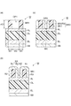
<ウエハ(密)>
・マスクMK1のマスク幅の値(W1[nm])と開口OP1の幅の値(W2[nm])との比(W1:W2):1対1(1:1)
・マスクMK1のマスク高の値(HG1[nm]):40[nm]
・マスクMK1の開口OP1の幅の値(W2[nm]):45.0[nm]
<ウエハ(疎)>
・マスクMK1のマスク幅の値(W1[nm])と開口OP1の幅の値(W2[nm])との比(W1:W2):1対5(1:5)
・マスクMK1のマスク高の値(HG1[nm]):40[nm]
・マスクMK1の開口OP1の幅の値(W2[nm]):225[nm]
<条件>
(反射防止膜ALのエッチング)
・処理容器12内の圧力の値[mTorr]:15[mTorr]
・第1の高周波電源62の周波数の値[MHz]および高周波電力の値[W]:60[MHz]、400[W]
・第2の高周波電源64の周波数の値[MHz]およびバイアス電力の値[W]:13.56[MHz]、100[W]
・処理ガス:CF4ガス
・処理ガスの流量[sccm]:150[sccm]
・処理時間[s]:30[s]
(有機膜OLのエッチング)
・処理容器12内の圧力の値[mTorr]:20[mTorr]
・第1の高周波電源62の周波数の値[MHz]および高周波電力の値[W]:60[MHz]、1000[W]
・第2の高周波電源64の周波数の値[MHz]およびバイアス電力の値[W]:13.56[MHz]、200[W]
・処理ガス:N2/H2ガス
・処理ガスの流量[sccm]:(N2ガス)200[sccm]、(H2ガス)200[sccm]
・処理時間[s]:40[s]
<条件>
(第1のガスを供給:工程ST6a)
・工程ST6aにおける処理容器12内の圧力の値[mTorr]:30[mTorr]
・工程ST6aにおける第1の高周波電源62の周波数の値[MHz]および高周波電力の値[W]:60[MHz]、100[W]
・工程ST6aにおける第2の高周波電源64の周波数の値[MHz]およびバイアス電力の値[W]:13.56[MHz]、0[W]
・電源70の直流電圧の値[V]:−1000[V]
・工程ST6aにおける処理ガス:CF4/Arガス
・工程ST6aにおける処理ガスの流量[sccm]:(CF4ガス)300[sccm]、(Arガス)300[sccm]
・工程ST6aにおける処理時間[s]:10[s]
(第2のガスのプラズマを生成:工程ST6c)
・工程ST6cにおける処理容器12内の圧力の値[mTorr]:30[mTorr]
・工程ST6cにおける第1の高周波電源62の周波数の値[MHz]および高周波電力の値[W]:60[MHz]、100[W]
・工程ST6cにおける第2の高周波電源64の周波数の値[MHz]およびバイアス電力の値[W]:13.56[MHz]、30[W]
・工程ST6cにおける処理ガス:Arガス
・工程ST6cにおける処理ガスの流量[sccm]:300[sccm]
・処理時間[s]:25[s]
(シーケンスSQ2の終了の判定:工程S7)
・シーケンスSQ2の繰り返し回数:30回
(有機膜OLをエッチング:工程ST8)
・処理容器12内の圧力の値[mTorr]:20[mTorr]
・第1の高周波電源62の周波数の値[MHz]および高周波電力の値[W]:60[MHz]、1000[W]
・第2の高周波電源64の周波数の値[MHz]およびバイアス電力の値[W]:13.56[MHz]、200[W]
・処理ガス:N2/H2ガス
・処理ガスの流量[sccm]:(N2ガス)200[sccm]、(H2ガス)200[sccm]
・処理時間[s]:45[s]
<条件>
(二次電子の照射:工程ST2)
・処理容器12内の圧力の値[mTorr]:30[mTorr]
・第1の高周波電源62の周波数の値[MHz]および高周波電力の値[W]:60[MHz]、100[W]
・第2の高周波電源64の周波数の値[MHz]およびバイアス電力の値[W]:13.56[MHz]、0[W]
・電源70の直流電圧の値[V]:−1000[V]
・処理ガス:H2/Arガス
・処理ガスの流量[sccm]:(H2ガス)60[sccm]、(Arガス)300[sccm]
・処理時間[s]:10[s]
(第1のガスを供給:工程ST3a)
・処理容器12内の圧力の値[mTorr]:500[mTorr]
・第1の高周波電源62の周波数の値[MHz]および高周波電力の値[W]:60[MHz]、0[W]
・第2の高周波電源64の周波数の値[MHz]およびバイアス電力の値[W]:13.56[MHz]、0[W]
・処理ガス:有機を含んだアミノシラン系ガス
・処理ガスの流量[sccm]:50[sccm]
・処理時間[s]:15[s]
(第2のガスを供給:工程ST3c)
・処理容器12内の圧力の値[mTorr]:200[mTorr]
・第1の高周波電源62の周波数の値[MHz]および高周波電力の値[W]:60[MHz]、300[W]
・パルス周波数:10[kHz]、50%
・第2の高周波電源64の周波数の値[MHz]およびバイアス電力の値[W]:13.56[MHz]、0[W]
・処理ガス:CO2ガス
・処理ガスの流量[sccm]:300[sccm]
・処理時間[s]:5[s]
(シーケンスSQ1の終了の判定:工程S4)
・シーケンスSQ1の繰り返し回数:20回
(エッチバック:工程ST5)
・処理容器12内の圧力の値[mTorr]:50[mTorr]
・第1の高周波電源62の周波数の値[MHz]および高周波電力の値[W]:60[MHz]、300[W]
・第2の高周波電源64の周波数の値[MHz]およびバイアス電力の値[W]:13.56[MHz]、150[W]
・電源70の直流電圧の値[V]:0[V]
・処理ガス:CF4ガス
・処理ガスの流量[sccm]:150[sccm]
・処理時間[s]:4[s]
(第3のガスのプラズマを生成:工程ST6a)
・工程ST6aにおける処理容器12内の圧力の値[mTorr]:30[mTorr]
・工程ST6aにおける第1の高周波電源62の周波数の値[MHz]および高周波電力の値[W]:60[MHz]、100[W]
・工程ST6aにおける第2の高周波電源64の周波数の値[MHz]およびバイアス電力の値[W]:13.56[MHz]、0[W]
・電源70の直流電圧の値[V]:−1000[V]
・工程ST6aにおける処理ガス:CF4/Arガス
・工程ST6aにおける処理ガスの流量[sccm]:(CF4ガス)300[sccm]、(Arガス)300[sccm]
・工程ST6aにおける処理時間[s]:10[s]
(第4のガスのプラズマを生成:工程ST6c)
・工程ST6cにおける処理容器12内の圧力の値[mTorr]:30[mTorr]
・工程ST6cにおける第1の高周波電源62の周波数の値[MHz]および高周波電力の値[W]:60[MHz]、100[W]
・工程ST6cにおける第2の高周波電源64の周波数の値[MHz]およびバイアス電力の値[W]:13.56[MHz]、0[W]
・電源70の直流電圧の値[V]:0[V]
・工程ST6cにおける処理ガス:Arガス
・工程ST6cにおける処理ガスの流量[sccm]:300[sccm]
・処理時間[s]:25[s]
(シーケンスSQ2の終了の判定:工程S7)
・シーケンスSQ2の繰り返し回数:30回
(有機膜OLのエッチング:工程ST8)
・処理容器12内の圧力の値[mTorr]:20[mTorr]
・第1の高周波電源62の周波数の値[MHz]および高周波電力の値[W]:60[MHz]、1000[W]
・第2の高周波電源64の周波数の値[MHz]およびバイアス電力の値[W]:13.56[MHz]、200[W]
・処理ガス:N2/H2ガス
・処理ガスの流量[sccm]:(N2ガス)200[sccm]、(H2ガス)200[sccm]
・処理時間[s]:45[s]
Claims (12)
- 被処理体を処理する方法であって、
前記被処理体は、被エッチング層と、該被エッチング層上に設けられた有機膜と、該有機膜上に設けられた反射防止膜と、該反射防止膜上に設けられた第1マスクと、を備え、
当該方法は、
前記被処理体が収容されたプラズマ処理装置の処理容器内において、前記第1マスクの表面に保護膜をコンフォーマルに形成する工程と、
前記保護膜をコンフォーマルに形成する前記工程の実行後に、該保護膜が形成された前記第1マスクを用いて、前記処理容器内で発生させたプラズマにより前記反射防止膜を原子層毎に除去し、該反射防止膜をエッチングする工程と、
を備える、
方法。 - 前記保護膜をコンフォーマルに形成する前記工程の実行前に、前記処理容器内でプラズマを発生させて前記処理容器に設けられた平行平板電極の上部電極に負の直流電圧を印可することにより、前記第1マスクに二次電子を照射する工程を更に備える、
請求項1に記載の方法。 - 前記上部電極の電極板は、シリコンを含有し、
前記第1マスクに二次電子を照射する前記工程は、前記処理容器内でプラズマを発生させて前記上部電極に負の直流電圧を印可することにより、前記電極板からシリコンを放出させて該シリコンを含む酸化シリコン化合物で前記第1マスクを覆う、
請求項2に記載の方法。 - 前記保護膜をコンフォーマルに形成する前記工程は、
前記処理容器内に第1のガスを供給する第1工程と、
前記第1工程の実行後に、前記処理容器内の空間をパージする第2工程と、
前記第2工程の実行後に、前記処理容器内において第2のガスのプラズマを生成する第3工程と、
前記第3工程の実行後に、前記処理容器内の空間をパージする第4工程と、
を含む第1シーケンスを繰り返し実行することによって、前記第1マスクの前記表面に前記保護膜をコンフォーマルに形成し、
前記第1工程は、前記第1のガスのプラズマを生成しない、
請求項1〜3の何れか一項に記載の方法。 - 前記第1のガスは、アミノシラン系ガスを含む、
請求項4に記載の方法。 - 前記第1のガスのアミノシラン系ガスは、1〜3個のケイ素原子を有するアミノシランを含む、請求項5に記載の方法。
- 前記第1のガスのアミノシラン系ガスは、1〜3個のアミノ基を有するアミノシランを含む、請求項5または請求項6に記載の方法。
- 前記第2のガスは、酸素原子および炭素原子を含有するガスを含む、
請求項4〜7の何れか一項に記載の方法。 - 前記反射防止膜をエッチングする前記工程は、
前記保護膜をコンフォーマルに形成する前記工程の実行後に、前記処理容器内において第3のガスのプラズマを生成し、該プラズマに含まれるラジカルを含む混合層を前記反射防止膜の表面の原子層に形成する第5工程と、
前記第5工程の実行後に、前記処理容器内の空間をパージする第6工程と、
前記第6工程の実行後に、前記処理容器内において第4のガスのプラズマを生成し、該プラズマにバイアス電圧を印可して、前記混合層を除去する第7工程と、
前記第7工程の実行後に、前記処理容器内の空間をパージする第8工程と、
を含む第2シーケンスを繰り返し実行し、前記反射防止膜を原子層毎に除去することによって、該反射防止膜をエッチングする、
請求項1〜8の何れか一項に記載の方法。 - 前記第3のガスは、フルオロカーボン系ガスと希ガスとを含む、
請求項9に記載の方法。 - 前記第4のガスは、希ガスを含む、
請求項9または請求項10に記載の方法。 - 前記反射防止膜をエッチングする前記工程の実行後に、前記処理容器内で発生させたプラズマにより、第2マスクを用いて前記有機膜に対しエッチング処理を行う工程を更に備え、
前記第2マスクは、前記反射防止膜をエッチングする前記工程において、前記第1マスクと該反射防止膜とから形成される、
請求項1〜11の何れか一項に記載の方法。
Priority Applications (8)
| Application Number | Priority Date | Filing Date | Title |
|---|---|---|---|
| TW106109250A TWI707382B (zh) | 2016-03-29 | 2017-03-21 | 被處理體之處理方法 |
| CN201780020010.3A CN108885991B (zh) | 2016-03-29 | 2017-03-27 | 对被处理物进行处理的方法 |
| PCT/JP2017/012407 WO2017170411A1 (ja) | 2016-03-29 | 2017-03-27 | 被処理体を処理する方法 |
| KR1020227004299A KR102549308B1 (ko) | 2016-03-29 | 2017-03-27 | 에칭 장치 |
| KR1020187030839A KR102362282B1 (ko) | 2016-03-29 | 2017-03-27 | 피처리체를 처리하는 방법 |
| US16/089,024 US10714340B2 (en) | 2016-03-29 | 2017-03-27 | Method for processing workpiece |
| US16/898,492 US11244828B2 (en) | 2016-03-29 | 2020-06-11 | Method for processing workpiece |
| US17/560,245 US11823903B2 (en) | 2016-03-29 | 2021-12-22 | Method for processing workpiece |
Applications Claiming Priority (2)
| Application Number | Priority Date | Filing Date | Title |
|---|---|---|---|
| JP2016065806 | 2016-03-29 | ||
| JP2016065806 | 2016-03-29 |
Related Child Applications (1)
| Application Number | Title | Priority Date | Filing Date |
|---|---|---|---|
| JP2020178083A Division JP7061653B2 (ja) | 2016-03-29 | 2020-10-23 | 被処理体を処理する方法 |
Publications (2)
| Publication Number | Publication Date |
|---|---|
| JP2017183689A JP2017183689A (ja) | 2017-10-05 |
| JP6784530B2 true JP6784530B2 (ja) | 2020-11-11 |
Family
ID=60008666
Family Applications (2)
| Application Number | Title | Priority Date | Filing Date |
|---|---|---|---|
| JP2016147477A Active JP6784530B2 (ja) | 2016-03-29 | 2016-07-27 | 被処理体を処理する方法 |
| JP2020178083A Active JP7061653B2 (ja) | 2016-03-29 | 2020-10-23 | 被処理体を処理する方法 |
Family Applications After (1)
| Application Number | Title | Priority Date | Filing Date |
|---|---|---|---|
| JP2020178083A Active JP7061653B2 (ja) | 2016-03-29 | 2020-10-23 | 被処理体を処理する方法 |
Country Status (4)
| Country | Link |
|---|---|
| US (1) | US10714340B2 (ja) |
| JP (2) | JP6784530B2 (ja) |
| CN (1) | CN108885991B (ja) |
| TW (1) | TWI707382B (ja) |
Families Citing this family (8)
| Publication number | Priority date | Publication date | Assignee | Title |
|---|---|---|---|---|
| US10658174B2 (en) * | 2017-11-21 | 2020-05-19 | Lam Research Corporation | Atomic layer deposition and etch for reducing roughness |
| JP7178918B2 (ja) * | 2019-01-30 | 2022-11-28 | 東京エレクトロン株式会社 | エッチング方法、プラズマ処理装置、及び処理システム |
| CN111627809B (zh) * | 2019-02-28 | 2024-03-22 | 东京毅力科创株式会社 | 基片处理方法和基片处理装置 |
| EP3842861B1 (en) * | 2019-12-23 | 2025-03-12 | IMEC vzw | A method for forming an euvl pellicle |
| US11401608B2 (en) * | 2020-10-20 | 2022-08-02 | Sky Tech Inc. | Atomic layer deposition equipment and process method |
| US11527413B2 (en) * | 2021-01-29 | 2022-12-13 | Tokyo Electron Limited | Cyclic plasma etch process |
| US12183579B2 (en) * | 2021-08-30 | 2024-12-31 | Taiwan Semiconductor Manufacturing Company, Ltd. | Method for manufacturing semiconductor device |
| TW202439443A (zh) * | 2023-03-27 | 2024-10-01 | 日商東京威力科創股份有限公司 | 蝕刻方法及電漿處理裝置 |
Family Cites Families (19)
| Publication number | Priority date | Publication date | Assignee | Title |
|---|---|---|---|---|
| ATE420454T1 (de) * | 1999-08-17 | 2009-01-15 | Tokyo Electron Ltd | Gepulstes plasmabehandlungsverfahren und vorrichtung |
| JPWO2004003988A1 (ja) * | 2002-06-27 | 2006-10-26 | 東京エレクトロン株式会社 | プラズマ処理方法 |
| US7169695B2 (en) * | 2002-10-11 | 2007-01-30 | Lam Research Corporation | Method for forming a dual damascene structure |
| JP2004228231A (ja) * | 2003-01-21 | 2004-08-12 | Matsushita Electric Ind Co Ltd | 半導体装置およびその製造方法 |
| KR100598105B1 (ko) | 2004-06-17 | 2006-07-07 | 삼성전자주식회사 | 반도체 패턴 형성 방법 |
| MY148830A (en) * | 2006-08-22 | 2013-06-14 | Lam Res Corp | Method for plasma etching performance enhancement |
| KR101217778B1 (ko) | 2007-06-08 | 2013-01-02 | 도쿄엘렉트론가부시키가이샤 | 패터닝 방법 |
| JP5528244B2 (ja) * | 2010-07-26 | 2014-06-25 | 東京エレクトロン株式会社 | プラズマ処理方法および記憶媒体 |
| US9184028B2 (en) | 2010-08-04 | 2015-11-10 | Lam Research Corporation | Dual plasma volume processing apparatus for neutral/ion flux control |
| US8993072B2 (en) * | 2011-09-27 | 2015-03-31 | Air Products And Chemicals, Inc. | Halogenated organoaminosilane precursors and methods for depositing films comprising same |
| US8900469B2 (en) | 2011-12-19 | 2014-12-02 | Applied Materials, Inc. | Etch rate detection for anti-reflective coating layer and absorber layer etching |
| JP6063264B2 (ja) * | 2012-09-13 | 2017-01-18 | 東京エレクトロン株式会社 | 被処理基体を処理する方法、及びプラズマ処理装置 |
| JP6120527B2 (ja) * | 2012-11-05 | 2017-04-26 | 東京エレクトロン株式会社 | プラズマ処理方法 |
| JP2014107520A (ja) * | 2012-11-30 | 2014-06-09 | Hitachi High-Technologies Corp | プラズマエッチング方法 |
| JP5519059B2 (ja) * | 2013-05-23 | 2014-06-11 | 株式会社日立国際電気 | 半導体デバイスの製造方法および基板処理装置 |
| US9685305B2 (en) * | 2013-08-09 | 2017-06-20 | Tokyo Electron Limited | Plasma processing apparatus and plasma processing method |
| JP6240489B2 (ja) * | 2013-12-06 | 2017-11-29 | 富士フイルム株式会社 | パターン形成方法、及び電子デバイスの製造方法 |
| JP6230898B2 (ja) * | 2013-12-13 | 2017-11-15 | 東京エレクトロン株式会社 | エッチング方法 |
| JP6770848B2 (ja) * | 2016-03-29 | 2020-10-21 | 東京エレクトロン株式会社 | 被処理体を処理する方法 |
-
2016
- 2016-07-27 JP JP2016147477A patent/JP6784530B2/ja active Active
-
2017
- 2017-03-21 TW TW106109250A patent/TWI707382B/zh active
- 2017-03-27 CN CN201780020010.3A patent/CN108885991B/zh active Active
- 2017-03-27 US US16/089,024 patent/US10714340B2/en active Active
-
2020
- 2020-10-23 JP JP2020178083A patent/JP7061653B2/ja active Active
Also Published As
| Publication number | Publication date |
|---|---|
| TW201807742A (zh) | 2018-03-01 |
| JP2017183689A (ja) | 2017-10-05 |
| JP2021007186A (ja) | 2021-01-21 |
| TWI707382B (zh) | 2020-10-11 |
| CN108885991A (zh) | 2018-11-23 |
| US10714340B2 (en) | 2020-07-14 |
| CN108885991B (zh) | 2023-06-30 |
| JP7061653B2 (ja) | 2022-04-28 |
| US20190108997A1 (en) | 2019-04-11 |
Similar Documents
| Publication | Publication Date | Title |
|---|---|---|
| JP7061653B2 (ja) | 被処理体を処理する方法 | |
| US10763123B2 (en) | Method for processing workpiece | |
| US9607811B2 (en) | Workpiece processing method | |
| US9911607B2 (en) | Method of processing target object | |
| KR102362462B1 (ko) | 피처리체를 처리하는 방법 | |
| KR102531901B1 (ko) | 피처리체를 처리하는 방법 | |
| KR102461750B1 (ko) | 피처리체를 처리하는 방법 | |
| US11823903B2 (en) | Method for processing workpiece |
Legal Events
| Date | Code | Title | Description |
|---|---|---|---|
| A621 | Written request for application examination |
Free format text: JAPANESE INTERMEDIATE CODE: A621 Effective date: 20190416 |
|
| A131 | Notification of reasons for refusal |
Free format text: JAPANESE INTERMEDIATE CODE: A131 Effective date: 20200204 |
|
| TRDD | Decision of grant or rejection written | ||
| A01 | Written decision to grant a patent or to grant a registration (utility model) |
Free format text: JAPANESE INTERMEDIATE CODE: A01 Effective date: 20200923 |
|
| A61 | First payment of annual fees (during grant procedure) |
Free format text: JAPANESE INTERMEDIATE CODE: A61 Effective date: 20201023 |
|
| R150 | Certificate of patent or registration of utility model |
Ref document number: 6784530 Country of ref document: JP Free format text: JAPANESE INTERMEDIATE CODE: R150 |
|
| R250 | Receipt of annual fees |
Free format text: JAPANESE INTERMEDIATE CODE: R250 |
|
| R250 | Receipt of annual fees |
Free format text: JAPANESE INTERMEDIATE CODE: R250 |
|
| R250 | Receipt of annual fees |
Free format text: JAPANESE INTERMEDIATE CODE: R250 |