JP6516995B2 - 発光素子、それを含む発光素子パッケージ及びパッケージを含む照明装置 - Google Patents
発光素子、それを含む発光素子パッケージ及びパッケージを含む照明装置 Download PDFInfo
- Publication number
- JP6516995B2 JP6516995B2 JP2014207390A JP2014207390A JP6516995B2 JP 6516995 B2 JP6516995 B2 JP 6516995B2 JP 2014207390 A JP2014207390 A JP 2014207390A JP 2014207390 A JP2014207390 A JP 2014207390A JP 6516995 B2 JP6516995 B2 JP 6516995B2
- Authority
- JP
- Japan
- Prior art keywords
- light emitting
- emitting device
- bumps
- disposed
- layer
- Prior art date
- Legal status (The legal status is an assumption and is not a legal conclusion. Google has not performed a legal analysis and makes no representation as to the accuracy of the status listed.)
- Active
Links
Images


Classifications
-
- H—ELECTRICITY
- H01—ELECTRIC ELEMENTS
- H01L—SEMICONDUCTOR DEVICES NOT COVERED BY CLASS H10
- H01L24/00—Arrangements for connecting or disconnecting semiconductor or solid-state bodies; Methods or apparatus related thereto
- H01L24/01—Means for bonding being attached to, or being formed on, the surface to be connected, e.g. chip-to-package, die-attach, "first-level" interconnects; Manufacturing methods related thereto
- H01L24/10—Bump connectors ; Manufacturing methods related thereto
- H01L24/12—Structure, shape, material or disposition of the bump connectors prior to the connecting process
- H01L24/14—Structure, shape, material or disposition of the bump connectors prior to the connecting process of a plurality of bump connectors
-
- F—MECHANICAL ENGINEERING; LIGHTING; HEATING; WEAPONS; BLASTING
- F21—LIGHTING
- F21K—NON-ELECTRIC LIGHT SOURCES USING LUMINESCENCE; LIGHT SOURCES USING ELECTROCHEMILUMINESCENCE; LIGHT SOURCES USING CHARGES OF COMBUSTIBLE MATERIAL; LIGHT SOURCES USING SEMICONDUCTOR DEVICES AS LIGHT-GENERATING ELEMENTS; LIGHT SOURCES NOT OTHERWISE PROVIDED FOR
- F21K9/00—Light sources using semiconductor devices as light-generating elements, e.g. using light-emitting diodes [LED] or lasers
-
- F—MECHANICAL ENGINEERING; LIGHTING; HEATING; WEAPONS; BLASTING
- F21—LIGHTING
- F21V—FUNCTIONAL FEATURES OR DETAILS OF LIGHTING DEVICES OR SYSTEMS THEREOF; STRUCTURAL COMBINATIONS OF LIGHTING DEVICES WITH OTHER ARTICLES, NOT OTHERWISE PROVIDED FOR
- F21V3/00—Globes; Bowls; Cover glasses
- F21V3/04—Globes; Bowls; Cover glasses characterised by materials, surface treatments or coatings
- F21V3/049—Patterns or structured surfaces for diffusing light, e.g. frosted surfaces
-
- F—MECHANICAL ENGINEERING; LIGHTING; HEATING; WEAPONS; BLASTING
- F21—LIGHTING
- F21V—FUNCTIONAL FEATURES OR DETAILS OF LIGHTING DEVICES OR SYSTEMS THEREOF; STRUCTURAL COMBINATIONS OF LIGHTING DEVICES WITH OTHER ARTICLES, NOT OTHERWISE PROVIDED FOR
- F21V3/00—Globes; Bowls; Cover glasses
- F21V3/04—Globes; Bowls; Cover glasses characterised by materials, surface treatments or coatings
- F21V3/10—Globes; Bowls; Cover glasses characterised by materials, surface treatments or coatings characterised by coatings
-
- G—PHYSICS
- G02—OPTICS
- G02B—OPTICAL ELEMENTS, SYSTEMS OR APPARATUS
- G02B6/00—Light guides; Structural details of arrangements comprising light guides and other optical elements, e.g. couplings
- G02B6/0001—Light guides; Structural details of arrangements comprising light guides and other optical elements, e.g. couplings specially adapted for lighting devices or systems
- G02B6/0011—Light guides; Structural details of arrangements comprising light guides and other optical elements, e.g. couplings specially adapted for lighting devices or systems the light guides being planar or of plate-like form
-
- H—ELECTRICITY
- H01—ELECTRIC ELEMENTS
- H01L—SEMICONDUCTOR DEVICES NOT COVERED BY CLASS H10
- H01L33/00—Semiconductor devices with at least one potential-jump barrier or surface barrier specially adapted for light emission; Processes or apparatus specially adapted for the manufacture or treatment thereof or of parts thereof; Details thereof
- H01L33/02—Semiconductor devices with at least one potential-jump barrier or surface barrier specially adapted for light emission; Processes or apparatus specially adapted for the manufacture or treatment thereof or of parts thereof; Details thereof characterised by the semiconductor bodies
- H01L33/08—Semiconductor devices with at least one potential-jump barrier or surface barrier specially adapted for light emission; Processes or apparatus specially adapted for the manufacture or treatment thereof or of parts thereof; Details thereof characterised by the semiconductor bodies with a plurality of light emitting regions, e.g. laterally discontinuous light emitting layer or photoluminescent region integrated within the semiconductor body
-
- H—ELECTRICITY
- H01—ELECTRIC ELEMENTS
- H01L—SEMICONDUCTOR DEVICES NOT COVERED BY CLASS H10
- H01L33/00—Semiconductor devices with at least one potential-jump barrier or surface barrier specially adapted for light emission; Processes or apparatus specially adapted for the manufacture or treatment thereof or of parts thereof; Details thereof
- H01L33/36—Semiconductor devices with at least one potential-jump barrier or surface barrier specially adapted for light emission; Processes or apparatus specially adapted for the manufacture or treatment thereof or of parts thereof; Details thereof characterised by the electrodes
-
- H—ELECTRICITY
- H01—ELECTRIC ELEMENTS
- H01L—SEMICONDUCTOR DEVICES NOT COVERED BY CLASS H10
- H01L33/00—Semiconductor devices with at least one potential-jump barrier or surface barrier specially adapted for light emission; Processes or apparatus specially adapted for the manufacture or treatment thereof or of parts thereof; Details thereof
- H01L33/48—Semiconductor devices with at least one potential-jump barrier or surface barrier specially adapted for light emission; Processes or apparatus specially adapted for the manufacture or treatment thereof or of parts thereof; Details thereof characterised by the semiconductor body packages
- H01L33/62—Arrangements for conducting electric current to or from the semiconductor body, e.g. lead-frames, wire-bonds or solder balls
-
- F—MECHANICAL ENGINEERING; LIGHTING; HEATING; WEAPONS; BLASTING
- F21—LIGHTING
- F21Y—INDEXING SCHEME ASSOCIATED WITH SUBCLASSES F21K, F21L, F21S and F21V, RELATING TO THE FORM OR THE KIND OF THE LIGHT SOURCES OR OF THE COLOUR OF THE LIGHT EMITTED
- F21Y2115/00—Light-generating elements of semiconductor light sources
- F21Y2115/10—Light-emitting diodes [LED]
-
- H—ELECTRICITY
- H01—ELECTRIC ELEMENTS
- H01L—SEMICONDUCTOR DEVICES NOT COVERED BY CLASS H10
- H01L2224/00—Indexing scheme for arrangements for connecting or disconnecting semiconductor or solid-state bodies and methods related thereto as covered by H01L24/00
- H01L2224/01—Means for bonding being attached to, or being formed on, the surface to be connected, e.g. chip-to-package, die-attach, "first-level" interconnects; Manufacturing methods related thereto
- H01L2224/10—Bump connectors; Manufacturing methods related thereto
- H01L2224/12—Structure, shape, material or disposition of the bump connectors prior to the connecting process
- H01L2224/13—Structure, shape, material or disposition of the bump connectors prior to the connecting process of an individual bump connector
- H01L2224/13001—Core members of the bump connector
- H01L2224/1301—Shape
- H01L2224/13012—Shape in top view
- H01L2224/13014—Shape in top view being circular or elliptic
-
- H—ELECTRICITY
- H01—ELECTRIC ELEMENTS
- H01L—SEMICONDUCTOR DEVICES NOT COVERED BY CLASS H10
- H01L2224/00—Indexing scheme for arrangements for connecting or disconnecting semiconductor or solid-state bodies and methods related thereto as covered by H01L24/00
- H01L2224/01—Means for bonding being attached to, or being formed on, the surface to be connected, e.g. chip-to-package, die-attach, "first-level" interconnects; Manufacturing methods related thereto
- H01L2224/10—Bump connectors; Manufacturing methods related thereto
- H01L2224/15—Structure, shape, material or disposition of the bump connectors after the connecting process
- H01L2224/16—Structure, shape, material or disposition of the bump connectors after the connecting process of an individual bump connector
- H01L2224/161—Disposition
- H01L2224/16135—Disposition the bump connector connecting between different semiconductor or solid-state bodies, i.e. chip-to-chip
- H01L2224/16145—Disposition the bump connector connecting between different semiconductor or solid-state bodies, i.e. chip-to-chip the bodies being stacked
-
- H—ELECTRICITY
- H01—ELECTRIC ELEMENTS
- H01L—SEMICONDUCTOR DEVICES NOT COVERED BY CLASS H10
- H01L2224/00—Indexing scheme for arrangements for connecting or disconnecting semiconductor or solid-state bodies and methods related thereto as covered by H01L24/00
- H01L2224/01—Means for bonding being attached to, or being formed on, the surface to be connected, e.g. chip-to-package, die-attach, "first-level" interconnects; Manufacturing methods related thereto
- H01L2224/42—Wire connectors; Manufacturing methods related thereto
- H01L2224/47—Structure, shape, material or disposition of the wire connectors after the connecting process
- H01L2224/48—Structure, shape, material or disposition of the wire connectors after the connecting process of an individual wire connector
- H01L2224/4805—Shape
- H01L2224/4809—Loop shape
- H01L2224/48091—Arched
-
- H—ELECTRICITY
- H01—ELECTRIC ELEMENTS
- H01L—SEMICONDUCTOR DEVICES NOT COVERED BY CLASS H10
- H01L2224/00—Indexing scheme for arrangements for connecting or disconnecting semiconductor or solid-state bodies and methods related thereto as covered by H01L24/00
- H01L2224/73—Means for bonding being of different types provided for in two or more of groups H01L2224/10, H01L2224/18, H01L2224/26, H01L2224/34, H01L2224/42, H01L2224/50, H01L2224/63, H01L2224/71
- H01L2224/732—Location after the connecting process
- H01L2224/73251—Location after the connecting process on different surfaces
- H01L2224/73265—Layer and wire connectors
-
- H—ELECTRICITY
- H01—ELECTRIC ELEMENTS
- H01L—SEMICONDUCTOR DEVICES NOT COVERED BY CLASS H10
- H01L2924/00—Indexing scheme for arrangements or methods for connecting or disconnecting semiconductor or solid-state bodies as covered by H01L24/00
- H01L2924/10—Details of semiconductor or other solid state devices to be connected
- H01L2924/11—Device type
- H01L2924/12—Passive devices, e.g. 2 terminal devices
- H01L2924/1204—Optical Diode
- H01L2924/12041—LED
-
- H—ELECTRICITY
- H01—ELECTRIC ELEMENTS
- H01L—SEMICONDUCTOR DEVICES NOT COVERED BY CLASS H10
- H01L2924/00—Indexing scheme for arrangements or methods for connecting or disconnecting semiconductor or solid-state bodies as covered by H01L24/00
- H01L2924/10—Details of semiconductor or other solid state devices to be connected
- H01L2924/11—Device type
- H01L2924/12—Passive devices, e.g. 2 terminal devices
- H01L2924/1204—Optical Diode
- H01L2924/12042—LASER
-
- H—ELECTRICITY
- H01—ELECTRIC ELEMENTS
- H01L—SEMICONDUCTOR DEVICES NOT COVERED BY CLASS H10
- H01L2924/00—Indexing scheme for arrangements or methods for connecting or disconnecting semiconductor or solid-state bodies as covered by H01L24/00
- H01L2924/15—Details of package parts other than the semiconductor or other solid state devices to be connected
- H01L2924/181—Encapsulation
-
- H—ELECTRICITY
- H01—ELECTRIC ELEMENTS
- H01L—SEMICONDUCTOR DEVICES NOT COVERED BY CLASS H10
- H01L33/00—Semiconductor devices with at least one potential-jump barrier or surface barrier specially adapted for light emission; Processes or apparatus specially adapted for the manufacture or treatment thereof or of parts thereof; Details thereof
- H01L33/02—Semiconductor devices with at least one potential-jump barrier or surface barrier specially adapted for light emission; Processes or apparatus specially adapted for the manufacture or treatment thereof or of parts thereof; Details thereof characterised by the semiconductor bodies
- H01L33/20—Semiconductor devices with at least one potential-jump barrier or surface barrier specially adapted for light emission; Processes or apparatus specially adapted for the manufacture or treatment thereof or of parts thereof; Details thereof characterised by the semiconductor bodies with a particular shape, e.g. curved or truncated substrate
-
- H—ELECTRICITY
- H01—ELECTRIC ELEMENTS
- H01L—SEMICONDUCTOR DEVICES NOT COVERED BY CLASS H10
- H01L33/00—Semiconductor devices with at least one potential-jump barrier or surface barrier specially adapted for light emission; Processes or apparatus specially adapted for the manufacture or treatment thereof or of parts thereof; Details thereof
- H01L33/36—Semiconductor devices with at least one potential-jump barrier or surface barrier specially adapted for light emission; Processes or apparatus specially adapted for the manufacture or treatment thereof or of parts thereof; Details thereof characterised by the electrodes
- H01L33/38—Semiconductor devices with at least one potential-jump barrier or surface barrier specially adapted for light emission; Processes or apparatus specially adapted for the manufacture or treatment thereof or of parts thereof; Details thereof characterised by the electrodes with a particular shape
Description
Claims (20)
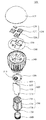
- 多角形の平面形状を有する発光素子であって、
基板と、
前記基板の下に配置され、第1導電型半導体層、活性層及び第2導電型半導体層を含む発光構造物と、
サブマウントと、
前記サブマウント上に互いに電気的に離隔して配置された第1及び第2金属パッドと、
前記第1導電型半導体層と前記第1金属パッドとの間に配置された複数個の第1バンプと、
前記第2導電型半導体層と前記第2金属パッドとの間に配置された複数個の第2バンプとを含み、
前記第1導電型半導体層、前記活性層及び前記複数個の第1バンプが配置された複数のアクティブ領域は、互いに離隔した平面形状を有し、
前記複数のアクティブ領域が互いに離隔した距離は、60μm〜300μmであり、
前記複数個の第1バンプは、前記複数個の第2バンプよりも前記発光素子の角に近接する第1バンプを複数含み、
前記複数個の第2バンプのそれぞれは、前記複数個の第1バンプのいずれか2つと隣接し、且つ、それらの間に配置され、
前記複数個の第2バンプのいずれか1つ及びこれに隣接する前記複数個の第1バンプのいずれか2つは、直線的に配列され、
前記複数個の第1バンプの個数は、前記複数個の第2バンプの個数以下である、発光素子。 - 前記複数のアクティブ領域は、前記発光素子のエッジから10μm〜100μmの距離だけ離隔した、請求項1に記載の発光素子。
- 前記複数のアクティブ領域が前記発光素子のエッジから離隔した距離は、互いに同一である、請求項1又は2に記載の発光素子。
- 前記複数のアクティブ領域が前記発光素子のエッジから離隔した距離は、互いに異なる、請求項1又は2に記載の発光素子。
- 前記複数個の第2バンプのそれぞれは、前記複数のアクティブ領域の間に配置された平面形状を有する、請求項1ないし4のいずれか1項に記載の発光素子。
- 前記複数個の第2バンプは、十字状に配置された平面形状を有する、請求項5に記載の発光素子。
- 前記複数個の第2バンプは、三角形状に配置された平面形状を有する、請求項5に記載の発光素子。
- 前記複数個の第1バンプのそれぞれは、円形の平面形状を有する、請求項1ないし7のいずれか1項に記載の発光素子。
- 前記複数個の第2バンプのそれぞれは、円形の平面形状を有する、請求項1ないし8のいずれか1項に記載の発光素子。
- 前記複数個の第2バンプのいずれかと前記第2導電型半導体層との間に配置された反射層をさらに含む、請求項1ないし9のいずれか1項に記載の発光素子。
- 前記複数のアクティブ領域のそれぞれを取り囲む環状の平面形状を有する反射層をさらに含む、請求項1ないし9のいずれか1項に記載の発光素子。
- 前記複数のアクティブ領域は、互いに等間隔に離隔して配置された平面形状を有する、請求項1ないし11のいずれか1項に記載の発光素子。
- 前記複数のアクティブ領域は、互いに異なる間隔で離隔して配置された平面形状を有する、請求項1ないし11のいずれか1項に記載の発光素子。
- 前記複数のアクティブ領域は、前記発光素子の周縁に配置された平面形状を有する、請求項1ないし13のいずれか1項に記載の発光素子。
- 前記活性層は、210nm〜280nmの波長帯域の光を放出する、請求項1ないし14のいずれか1項に記載の発光素子。
- 前記複数個の第1バンプの個数と前記複数個の第2バンプの個数とは同一である、請求項15に記載の発光素子。
- 前記複数個の第1バンプの個数と前記複数個の第2バンプの個数とは互いに異なる、請求項15に記載の発光素子。
- 前記複数個の第1バンプのそれぞれの第1高さは、前記複数個の第2バンプのそれぞれの第2高さよりも小さい、請求項1ないし17のいずれか1項に記載の発光素子。
- ヘッダーと、
前記ヘッダー上に配置されてキャビティを形成する側壁部と、
前記ヘッダー上で前記キャビティ内に配置された請求項1ないし18のいずれか1項に記載の前記発光素子の前記第1及び第2金属パッドと電気的にそれぞれ接続される第1及び第2ワイヤと、
前記第1及び第2ワイヤを介して前記第1及び第2金属パッドとそれぞれ電気的に接続される第1及び第2リード線と、
前記キャビティに充填されて前記発光素子を包囲するように配置されたモールディング部材とを含む、発光素子パッケージ。 - 請求項19に記載の発光素子パッケージと、
前記発光素子パッケージから提供される光を拡散、散乱または励起させるカバーとを含む、照明装置。
Applications Claiming Priority (2)
| Application Number | Priority Date | Filing Date | Title |
|---|---|---|---|
| KR1020130119754A KR102099439B1 (ko) | 2013-10-08 | 2013-10-08 | 발광 소자 및 이를 포함하는 발광 소자 패키지 |
| KR10-2013-0119754 | 2013-10-08 |
Publications (3)
| Publication Number | Publication Date |
|---|---|
| JP2015076617A JP2015076617A (ja) | 2015-04-20 |
| JP2015076617A5 JP2015076617A5 (ja) | 2017-11-16 |
| JP6516995B2 true JP6516995B2 (ja) | 2019-05-22 |
Family
ID=51660390
Family Applications (1)
| Application Number | Title | Priority Date | Filing Date |
|---|---|---|---|
| JP2014207390A Active JP6516995B2 (ja) | 2013-10-08 | 2014-10-08 | 発光素子、それを含む発光素子パッケージ及びパッケージを含む照明装置 |
Country Status (5)
| Country | Link |
|---|---|
| US (1) | US9627596B2 (ja) |
| EP (1) | EP2860778B1 (ja) |
| JP (1) | JP6516995B2 (ja) |
| KR (1) | KR102099439B1 (ja) |
| CN (1) | CN104518063B (ja) |
Families Citing this family (10)
| Publication number | Priority date | Publication date | Assignee | Title |
|---|---|---|---|---|
| JP6156402B2 (ja) | 2015-02-13 | 2017-07-05 | 日亜化学工業株式会社 | 発光装置 |
| DE102015112438A1 (de) | 2015-07-29 | 2017-02-02 | SMR Patents S.à.r.l. | Beleuchtungsvorrichtung zur optimierten Lichtverteilung |
| JP6696298B2 (ja) * | 2015-07-30 | 2020-05-20 | 日亜化学工業株式会社 | 発光素子及びそれを用いた発光装置 |
| US9786812B2 (en) * | 2015-07-30 | 2017-10-10 | Nichia Corporation | Light emitting element and light emitting device |
| JP6555043B2 (ja) * | 2015-09-18 | 2019-08-07 | 日亜化学工業株式会社 | 発光素子及び発光装置 |
| WO2018038105A1 (ja) * | 2016-08-26 | 2018-03-01 | スタンレー電気株式会社 | Iii族窒化物半導体発光素子 |
| JP6555247B2 (ja) * | 2016-12-28 | 2019-08-07 | 日亜化学工業株式会社 | 発光装置及びその製造方法 |
| DE102018101974A1 (de) | 2018-01-30 | 2019-08-01 | Infrasolid Gmbh | Infrarotstrahlungsquelle |
| CN112698528A (zh) * | 2019-10-22 | 2021-04-23 | 京东方科技集团股份有限公司 | 一种背光模组及显示装置 |
| KR20210047695A (ko) * | 2019-10-22 | 2021-04-30 | 삼성전자주식회사 | 발광 다이오드와 백플레인과 이들을 포함하는 led 디스플레이 |
Family Cites Families (36)
| Publication number | Priority date | Publication date | Assignee | Title |
|---|---|---|---|---|
| JPH01214141A (ja) * | 1988-02-23 | 1989-08-28 | Nec Corp | フリップチップ型半導体装置 |
| CN100595938C (zh) | 2002-08-01 | 2010-03-24 | 日亚化学工业株式会社 | 半导体发光元件及其制造方法、使用此的发光装置 |
| US6977396B2 (en) | 2003-02-19 | 2005-12-20 | Lumileds Lighting U.S., Llc | High-powered light emitting device with improved thermal properties |
| US7141828B2 (en) * | 2003-03-19 | 2006-11-28 | Gelcore, Llc | Flip-chip light emitting diode with a thermally stable multiple layer reflective p-type contact |
| JP2005012206A (ja) * | 2003-05-29 | 2005-01-13 | Mitsubishi Cable Ind Ltd | 窒化物系半導体素子およびその製造方法 |
| KR100576855B1 (ko) * | 2003-12-20 | 2006-05-10 | 삼성전기주식회사 | 고출력 플립 칩 발광다이오드 |
| TWI223457B (en) * | 2004-01-20 | 2004-11-01 | Opto Tech Corp | Light-emitting device to increase the area of active region |
| US7683391B2 (en) * | 2004-05-26 | 2010-03-23 | Lockheed Martin Corporation | UV emitting LED having mesa structure |
| KR20050113736A (ko) * | 2004-05-31 | 2005-12-05 | 엘지이노텍 주식회사 | 발광 다이오드 패키지 |
| JP4345591B2 (ja) | 2004-06-30 | 2009-10-14 | 豊田合成株式会社 | 発光装置 |
| US7812360B2 (en) * | 2004-10-04 | 2010-10-12 | Kabushiki Kaisha Toshiba | Light emitting device, lighting equipment or liquid crystal display device using such light emitting device |
| US20060138443A1 (en) * | 2004-12-23 | 2006-06-29 | Iii-N Technology, Inc. | Encapsulation and packaging of ultraviolet and deep-ultraviolet light emitting diodes |
| WO2006095949A1 (en) * | 2005-03-11 | 2006-09-14 | Seoul Semiconductor Co., Ltd. | Led package having an array of light emitting cells coupled in series |
| KR100597166B1 (ko) * | 2005-05-03 | 2006-07-04 | 삼성전기주식회사 | 플립 칩 발광다이오드 및 그 제조방법 |
| CN100570911C (zh) * | 2005-07-15 | 2009-12-16 | 松下电器产业株式会社 | 半导体发光元件以及半导体发光元件安装完成基板 |
| US7847302B2 (en) * | 2005-08-26 | 2010-12-07 | Koninklijke Philips Electronics, N.V. | Blue LED with phosphor layer for producing white light and different phosphor in outer lens for reducing color temperature |
| US7659546B2 (en) * | 2005-12-23 | 2010-02-09 | Hong Kong Applied Science And Technology Research Institute Co., Ltd. | Light emitting device |
| JP2007324577A (ja) * | 2006-05-01 | 2007-12-13 | Mitsubishi Chemicals Corp | 集積型半導体発光装置およびその製造方法 |
| JP5125795B2 (ja) * | 2007-07-18 | 2013-01-23 | 日亜化学工業株式会社 | 半導体発光素子および発光装置 |
| DE102009034359A1 (de) * | 2009-07-17 | 2011-02-17 | Forschungsverbund Berlin E.V. | P-Kontakt und Leuchtdiode für den ultravioletten Spektralbereich |
| US20110062454A1 (en) * | 2009-09-11 | 2011-03-17 | Hong Kong Applied Science And Technology Research Institute Co., Ltd. | Light emitting device having remotely located light scattering material |
| JP2011181576A (ja) | 2010-02-26 | 2011-09-15 | Citizen Holdings Co Ltd | 半導体発光素子及びそれを用いた半導体発光装置 |
| JP5849215B2 (ja) * | 2010-06-21 | 2016-01-27 | パナソニックIpマネジメント株式会社 | 紫外半導体発光素子 |
| KR101171361B1 (ko) * | 2010-11-05 | 2012-08-10 | 서울옵토디바이스주식회사 | 발광 다이오드 어셈블리 및 그의 제조 방법 |
| JP5475732B2 (ja) * | 2011-02-21 | 2014-04-16 | 株式会社東芝 | 照明装置 |
| JP2013012559A (ja) * | 2011-06-29 | 2013-01-17 | Nichia Chem Ind Ltd | 発光素子の製造方法 |
| JP5575715B2 (ja) * | 2011-08-29 | 2014-08-20 | 日立アプライアンス株式会社 | 電球型照明装置 |
| JP5747741B2 (ja) * | 2011-08-30 | 2015-07-15 | 豊田合成株式会社 | 半導体発光チップの製造方法 |
| US9847372B2 (en) * | 2011-12-01 | 2017-12-19 | Micron Technology, Inc. | Solid state transducer devices with separately controlled regions, and associated systems and methods |
| EP2605295A3 (en) * | 2011-12-13 | 2015-11-11 | LG Innotek Co., Ltd. | Ultraviolet light emitting device |
| KR20130098048A (ko) * | 2012-02-27 | 2013-09-04 | 엘지이노텍 주식회사 | 발광소자 패키지 |
| JP2013197456A (ja) * | 2012-03-22 | 2013-09-30 | Stanley Electric Co Ltd | Ledアレイ及び車両用灯具 |
| KR20130128931A (ko) * | 2012-05-18 | 2013-11-27 | 삼성전자주식회사 | N형 알루미늄 갈륨 나이트라이드 박막 및 자외선 발광소자 |
| KR102075147B1 (ko) * | 2013-06-05 | 2020-02-10 | 엘지이노텍 주식회사 | 발광 소자 및 발광 소자 패키지 |
| KR102075655B1 (ko) * | 2013-06-24 | 2020-02-10 | 엘지이노텍 주식회사 | 발광 소자 및 발광 소자 패키지 |
| US10283681B2 (en) * | 2013-09-12 | 2019-05-07 | Cree, Inc. | Phosphor-converted light emitting device |
-
2013
- 2013-10-08 KR KR1020130119754A patent/KR102099439B1/ko active IP Right Grant
-
2014
- 2014-10-08 JP JP2014207390A patent/JP6516995B2/ja active Active
- 2014-10-08 EP EP14188064.1A patent/EP2860778B1/en active Active
- 2014-10-08 CN CN201410525074.7A patent/CN104518063B/zh active Active
- 2014-10-08 US US14/509,195 patent/US9627596B2/en active Active
Also Published As
| Publication number | Publication date |
|---|---|
| EP2860778B1 (en) | 2020-12-09 |
| KR20150041344A (ko) | 2015-04-16 |
| CN104518063B (zh) | 2019-01-22 |
| EP2860778A1 (en) | 2015-04-15 |
| US9627596B2 (en) | 2017-04-18 |
| US20150098224A1 (en) | 2015-04-09 |
| KR102099439B1 (ko) | 2020-04-09 |
| JP2015076617A (ja) | 2015-04-20 |
| CN104518063A (zh) | 2015-04-15 |
Similar Documents
| Publication | Publication Date | Title |
|---|---|---|
| JP6516995B2 (ja) | 発光素子、それを含む発光素子パッケージ及びパッケージを含む照明装置 | |
| KR102197082B1 (ko) | 발광 소자 및 이를 포함하는 발광소자 패키지 | |
| KR101992366B1 (ko) | 발광 소자 | |
| KR102080778B1 (ko) | 발광 소자 패키지 | |
| KR102087935B1 (ko) | 발광 소자 | |
| KR102066620B1 (ko) | 발광 소자 | |
| KR20150012950A (ko) | 발광 소자 패키지 | |
| KR102076241B1 (ko) | 자외선 발광 소자 | |
| KR102050056B1 (ko) | 발광 소자 | |
| KR102114935B1 (ko) | 발광소자 모듈 | |
| KR102140273B1 (ko) | 발광 소자 및 이를 포함하는 발광 소자 패키지 | |
| KR102114932B1 (ko) | 발광 소자 및 이를 포함하는 발광 소자 패키지 | |
| KR102080779B1 (ko) | 발광 소자 | |
| KR102194804B1 (ko) | 발광 소자 | |
| KR20150040630A (ko) | 발광 소자 | |
| KR102256629B1 (ko) | 발광 소자 및 발광 소자 패키지 | |
| KR102076240B1 (ko) | 발광 소자 | |
| KR102087937B1 (ko) | 발광 소자 | |
| KR102387253B1 (ko) | 발광 소자 | |
| KR102127444B1 (ko) | 발광 소자 | |
| KR102024292B1 (ko) | 발광 소자 패키지 | |
| KR102038442B1 (ko) | 발광 소자 | |
| KR102170218B1 (ko) | 발광소자 패키지 | |
| KR102050057B1 (ko) | 발광 소자 패키지 | |
| KR20150137298A (ko) | 발광 소자 패키지 |
Legal Events
| Date | Code | Title | Description |
|---|---|---|---|
| A521 | Request for written amendment filed |
Free format text: JAPANESE INTERMEDIATE CODE: A523 Effective date: 20170927 |
|
| A621 | Written request for application examination |
Free format text: JAPANESE INTERMEDIATE CODE: A621 Effective date: 20170927 |
|
| A131 | Notification of reasons for refusal |
Free format text: JAPANESE INTERMEDIATE CODE: A131 Effective date: 20180731 |
|
| A977 | Report on retrieval |
Free format text: JAPANESE INTERMEDIATE CODE: A971007 Effective date: 20180731 |
|
| A521 | Request for written amendment filed |
Free format text: JAPANESE INTERMEDIATE CODE: A523 Effective date: 20181026 |
|
| TRDD | Decision of grant or rejection written | ||
| A01 | Written decision to grant a patent or to grant a registration (utility model) |
Free format text: JAPANESE INTERMEDIATE CODE: A01 Effective date: 20190319 |
|
| A61 | First payment of annual fees (during grant procedure) |
Free format text: JAPANESE INTERMEDIATE CODE: A61 Effective date: 20190417 |
|
| R150 | Certificate of patent or registration of utility model |
Ref document number: 6516995 Country of ref document: JP Free format text: JAPANESE INTERMEDIATE CODE: R150 |
|
| S531 | Written request for registration of change of domicile |
Free format text: JAPANESE INTERMEDIATE CODE: R313531 |
|
| S111 | Request for change of ownership or part of ownership |
Free format text: JAPANESE INTERMEDIATE CODE: R313113 |
|
| R350 | Written notification of registration of transfer |
Free format text: JAPANESE INTERMEDIATE CODE: R350 |
|
| R350 | Written notification of registration of transfer |
Free format text: JAPANESE INTERMEDIATE CODE: R350 |
|
| R250 | Receipt of annual fees |
Free format text: JAPANESE INTERMEDIATE CODE: R250 |
|
| R250 | Receipt of annual fees |
Free format text: JAPANESE INTERMEDIATE CODE: R250 |