JP6482425B2 - ウエーハの薄化方法 - Google Patents
ウエーハの薄化方法 Download PDFInfo
- Publication number
- JP6482425B2 JP6482425B2 JP2015144350A JP2015144350A JP6482425B2 JP 6482425 B2 JP6482425 B2 JP 6482425B2 JP 2015144350 A JP2015144350 A JP 2015144350A JP 2015144350 A JP2015144350 A JP 2015144350A JP 6482425 B2 JP6482425 B2 JP 6482425B2
- Authority
- JP
- Japan
- Prior art keywords
- wafer
- thinning
- laser beam
- starting point
- modified layer
- Prior art date
- Legal status (The legal status is an assumption and is not a legal conclusion. Google has not performed a legal analysis and makes no representation as to the accuracy of the status listed.)
- Active
Links
Images


Classifications
-
- H—ELECTRICITY
- H10—SEMICONDUCTOR DEVICES; ELECTRIC SOLID-STATE DEVICES NOT OTHERWISE PROVIDED FOR
- H10P—GENERIC PROCESSES OR APPARATUS FOR THE MANUFACTURE OR TREATMENT OF DEVICES COVERED BY CLASS H10
- H10P50/00—Etching of wafers, substrates or parts of devices
-
- B—PERFORMING OPERATIONS; TRANSPORTING
- B28—WORKING CEMENT, CLAY, OR STONE
- B28D—WORKING STONE OR STONE-LIKE MATERIALS
- B28D5/00—Fine working of gems, jewels, crystals, e.g. of semiconductor material; apparatus or devices therefor
-
- H—ELECTRICITY
- H10—SEMICONDUCTOR DEVICES; ELECTRIC SOLID-STATE DEVICES NOT OTHERWISE PROVIDED FOR
- H10P—GENERIC PROCESSES OR APPARATUS FOR THE MANUFACTURE OR TREATMENT OF DEVICES COVERED BY CLASS H10
- H10P54/00—Cutting or separating of wafers, substrates or parts of devices
-
- B—PERFORMING OPERATIONS; TRANSPORTING
- B23—MACHINE TOOLS; METAL-WORKING NOT OTHERWISE PROVIDED FOR
- B23K—SOLDERING OR UNSOLDERING; WELDING; CLADDING OR PLATING BY SOLDERING OR WELDING; CUTTING BY APPLYING HEAT LOCALLY, e.g. FLAME CUTTING; WORKING BY LASER BEAM
- B23K26/00—Working by laser beam, e.g. welding, cutting or boring
- B23K26/0006—Working by laser beam, e.g. welding, cutting or boring taking account of the properties of the material involved
-
- B—PERFORMING OPERATIONS; TRANSPORTING
- B23—MACHINE TOOLS; METAL-WORKING NOT OTHERWISE PROVIDED FOR
- B23K—SOLDERING OR UNSOLDERING; WELDING; CLADDING OR PLATING BY SOLDERING OR WELDING; CUTTING BY APPLYING HEAT LOCALLY, e.g. FLAME CUTTING; WORKING BY LASER BEAM
- B23K26/00—Working by laser beam, e.g. welding, cutting or boring
- B23K26/02—Positioning or observing the workpiece, e.g. with respect to the point of impact; Aligning, aiming or focusing the laser beam
- B23K26/03—Observing, e.g. monitoring, the workpiece
- B23K26/032—Observing, e.g. monitoring, the workpiece using optical means
-
- B—PERFORMING OPERATIONS; TRANSPORTING
- B23—MACHINE TOOLS; METAL-WORKING NOT OTHERWISE PROVIDED FOR
- B23K—SOLDERING OR UNSOLDERING; WELDING; CLADDING OR PLATING BY SOLDERING OR WELDING; CUTTING BY APPLYING HEAT LOCALLY, e.g. FLAME CUTTING; WORKING BY LASER BEAM
- B23K26/00—Working by laser beam, e.g. welding, cutting or boring
- B23K26/02—Positioning or observing the workpiece, e.g. with respect to the point of impact; Aligning, aiming or focusing the laser beam
- B23K26/06—Shaping the laser beam, e.g. by masks or multi-focusing
- B23K26/062—Shaping the laser beam, e.g. by masks or multi-focusing by direct control of the laser beam
- B23K26/0622—Shaping the laser beam, e.g. by masks or multi-focusing by direct control of the laser beam by shaping pulses
-
- B—PERFORMING OPERATIONS; TRANSPORTING
- B23—MACHINE TOOLS; METAL-WORKING NOT OTHERWISE PROVIDED FOR
- B23K—SOLDERING OR UNSOLDERING; WELDING; CLADDING OR PLATING BY SOLDERING OR WELDING; CUTTING BY APPLYING HEAT LOCALLY, e.g. FLAME CUTTING; WORKING BY LASER BEAM
- B23K26/00—Working by laser beam, e.g. welding, cutting or boring
- B23K26/08—Devices involving relative movement between laser beam and workpiece
- B23K26/0823—Devices involving rotation of the workpiece
-
- B—PERFORMING OPERATIONS; TRANSPORTING
- B23—MACHINE TOOLS; METAL-WORKING NOT OTHERWISE PROVIDED FOR
- B23K—SOLDERING OR UNSOLDERING; WELDING; CLADDING OR PLATING BY SOLDERING OR WELDING; CUTTING BY APPLYING HEAT LOCALLY, e.g. FLAME CUTTING; WORKING BY LASER BEAM
- B23K26/00—Working by laser beam, e.g. welding, cutting or boring
- B23K26/08—Devices involving relative movement between laser beam and workpiece
- B23K26/083—Devices involving movement of the workpiece in at least one axial direction
- B23K26/0853—Devices involving movement of the workpiece in at least two axial directions, e.g. in a plane
-
- B—PERFORMING OPERATIONS; TRANSPORTING
- B23—MACHINE TOOLS; METAL-WORKING NOT OTHERWISE PROVIDED FOR
- B23K—SOLDERING OR UNSOLDERING; WELDING; CLADDING OR PLATING BY SOLDERING OR WELDING; CUTTING BY APPLYING HEAT LOCALLY, e.g. FLAME CUTTING; WORKING BY LASER BEAM
- B23K26/00—Working by laser beam, e.g. welding, cutting or boring
- B23K26/36—Removing material
- B23K26/38—Removing material by boring or cutting
-
- B—PERFORMING OPERATIONS; TRANSPORTING
- B23—MACHINE TOOLS; METAL-WORKING NOT OTHERWISE PROVIDED FOR
- B23K—SOLDERING OR UNSOLDERING; WELDING; CLADDING OR PLATING BY SOLDERING OR WELDING; CUTTING BY APPLYING HEAT LOCALLY, e.g. FLAME CUTTING; WORKING BY LASER BEAM
- B23K26/00—Working by laser beam, e.g. welding, cutting or boring
- B23K26/50—Working by transmitting the laser beam through or within the workpiece
- B23K26/53—Working by transmitting the laser beam through or within the workpiece for modifying or reforming the material inside the workpiece, e.g. for producing break initiation cracks
-
- B—PERFORMING OPERATIONS; TRANSPORTING
- B23—MACHINE TOOLS; METAL-WORKING NOT OTHERWISE PROVIDED FOR
- B23K—SOLDERING OR UNSOLDERING; WELDING; CLADDING OR PLATING BY SOLDERING OR WELDING; CUTTING BY APPLYING HEAT LOCALLY, e.g. FLAME CUTTING; WORKING BY LASER BEAM
- B23K26/00—Working by laser beam, e.g. welding, cutting or boring
- B23K26/60—Preliminary treatment
-
- B—PERFORMING OPERATIONS; TRANSPORTING
- B23—MACHINE TOOLS; METAL-WORKING NOT OTHERWISE PROVIDED FOR
- B23K—SOLDERING OR UNSOLDERING; WELDING; CLADDING OR PLATING BY SOLDERING OR WELDING; CUTTING BY APPLYING HEAT LOCALLY, e.g. FLAME CUTTING; WORKING BY LASER BEAM
- B23K26/00—Working by laser beam, e.g. welding, cutting or boring
- B23K26/70—Auxiliary operations or equipment
- B23K26/702—Auxiliary equipment
-
- B—PERFORMING OPERATIONS; TRANSPORTING
- B24—GRINDING; POLISHING
- B24B—MACHINES, DEVICES, OR PROCESSES FOR GRINDING OR POLISHING; DRESSING OR CONDITIONING OF ABRADING SURFACES; FEEDING OF GRINDING, POLISHING, OR LAPPING AGENTS
- B24B7/00—Machines or devices designed for grinding plane surfaces on work, including polishing plane glass surfaces; Accessories therefor
- B24B7/20—Machines or devices designed for grinding plane surfaces on work, including polishing plane glass surfaces; Accessories therefor characterised by a special design with respect to properties of the material of non-metallic articles to be ground
- B24B7/22—Machines or devices designed for grinding plane surfaces on work, including polishing plane glass surfaces; Accessories therefor characterised by a special design with respect to properties of the material of non-metallic articles to be ground for grinding inorganic material, e.g. stone, ceramics, porcelain
- B24B7/228—Machines or devices designed for grinding plane surfaces on work, including polishing plane glass surfaces; Accessories therefor characterised by a special design with respect to properties of the material of non-metallic articles to be ground for grinding inorganic material, e.g. stone, ceramics, porcelain for grinding thin, brittle parts, e.g. semiconductors, wafers
-
- B—PERFORMING OPERATIONS; TRANSPORTING
- B28—WORKING CEMENT, CLAY, OR STONE
- B28D—WORKING STONE OR STONE-LIKE MATERIALS
- B28D5/00—Fine working of gems, jewels, crystals, e.g. of semiconductor material; apparatus or devices therefor
- B28D5/0005—Fine working of gems, jewels, crystals, e.g. of semiconductor material; apparatus or devices therefor by breaking, e.g. dicing
- B28D5/0011—Fine working of gems, jewels, crystals, e.g. of semiconductor material; apparatus or devices therefor by breaking, e.g. dicing with preliminary treatment, e.g. weakening by scoring
-
- H—ELECTRICITY
- H10—SEMICONDUCTOR DEVICES; ELECTRIC SOLID-STATE DEVICES NOT OTHERWISE PROVIDED FOR
- H10D—INORGANIC ELECTRIC SEMICONDUCTOR DEVICES
- H10D62/00—Semiconductor bodies, or regions thereof, of devices having potential barriers
- H10D62/80—Semiconductor bodies, or regions thereof, of devices having potential barriers characterised by the materials
- H10D62/83—Semiconductor bodies, or regions thereof, of devices having potential barriers characterised by the materials being Group IV materials, e.g. B-doped Si or undoped Ge
- H10D62/832—Semiconductor bodies, or regions thereof, of devices having potential barriers characterised by the materials being Group IV materials, e.g. B-doped Si or undoped Ge being Group IV materials comprising two or more elements, e.g. SiGe
- H10D62/8325—Silicon carbide
-
- H—ELECTRICITY
- H10—SEMICONDUCTOR DEVICES; ELECTRIC SOLID-STATE DEVICES NOT OTHERWISE PROVIDED FOR
- H10P—GENERIC PROCESSES OR APPARATUS FOR THE MANUFACTURE OR TREATMENT OF DEVICES COVERED BY CLASS H10
- H10P14/00—Formation of materials, e.g. in the shape of layers or pillars
- H10P14/20—Formation of materials, e.g. in the shape of layers or pillars of semiconductor materials
- H10P14/29—Formation of materials, e.g. in the shape of layers or pillars of semiconductor materials characterised by the substrates
- H10P14/2901—Materials
- H10P14/2902—Materials being Group IVA materials
- H10P14/2904—Silicon carbide
-
- H—ELECTRICITY
- H10—SEMICONDUCTOR DEVICES; ELECTRIC SOLID-STATE DEVICES NOT OTHERWISE PROVIDED FOR
- H10P—GENERIC PROCESSES OR APPARATUS FOR THE MANUFACTURE OR TREATMENT OF DEVICES COVERED BY CLASS H10
- H10P34/00—Irradiation with electromagnetic or particle radiation of wafers, substrates or parts of devices
- H10P34/40—Irradiation with electromagnetic or particle radiation of wafers, substrates or parts of devices with high-energy radiation
- H10P34/42—Irradiation with electromagnetic or particle radiation of wafers, substrates or parts of devices with high-energy radiation with electromagnetic radiation, e.g. laser annealing
-
- H—ELECTRICITY
- H10—SEMICONDUCTOR DEVICES; ELECTRIC SOLID-STATE DEVICES NOT OTHERWISE PROVIDED FOR
- H10P—GENERIC PROCESSES OR APPARATUS FOR THE MANUFACTURE OR TREATMENT OF DEVICES COVERED BY CLASS H10
- H10P52/00—Grinding, lapping or polishing of wafers, substrates or parts of devices
-
- H—ELECTRICITY
- H10—SEMICONDUCTOR DEVICES; ELECTRIC SOLID-STATE DEVICES NOT OTHERWISE PROVIDED FOR
- H10P—GENERIC PROCESSES OR APPARATUS FOR THE MANUFACTURE OR TREATMENT OF DEVICES COVERED BY CLASS H10
- H10P72/00—Handling or holding of wafers, substrates or devices during manufacture or treatment thereof
- H10P72/70—Handling or holding of wafers, substrates or devices during manufacture or treatment thereof for supporting or gripping
- H10P72/74—Handling or holding of wafers, substrates or devices during manufacture or treatment thereof for supporting or gripping using temporarily an auxiliary support
- H10P72/7402—Wafer tapes, e.g. grinding or dicing support tapes
-
- H—ELECTRICITY
- H10—SEMICONDUCTOR DEVICES; ELECTRIC SOLID-STATE DEVICES NOT OTHERWISE PROVIDED FOR
- H10P—GENERIC PROCESSES OR APPARATUS FOR THE MANUFACTURE OR TREATMENT OF DEVICES COVERED BY CLASS H10
- H10P90/00—Preparation of wafers not covered by a single main group of this subclass, e.g. wafer reinforcement
- H10P90/12—Preparing bulk and homogeneous wafers
- H10P90/123—Preparing bulk and homogeneous wafers by grinding or lapping
-
- H—ELECTRICITY
- H10—SEMICONDUCTOR DEVICES; ELECTRIC SOLID-STATE DEVICES NOT OTHERWISE PROVIDED FOR
- H10W—GENERIC PACKAGES, INTERCONNECTIONS, CONNECTORS OR OTHER CONSTRUCTIONAL DETAILS OF DEVICES COVERED BY CLASS H10
- H10W10/00—Isolation regions in semiconductor bodies between components of integrated devices
- H10W10/01—Manufacture or treatment
-
- B—PERFORMING OPERATIONS; TRANSPORTING
- B23—MACHINE TOOLS; METAL-WORKING NOT OTHERWISE PROVIDED FOR
- B23K—SOLDERING OR UNSOLDERING; WELDING; CLADDING OR PLATING BY SOLDERING OR WELDING; CUTTING BY APPLYING HEAT LOCALLY, e.g. FLAME CUTTING; WORKING BY LASER BEAM
- B23K2101/00—Articles made by soldering, welding or cutting
- B23K2101/36—Electric or electronic devices
- B23K2101/40—Semiconductor devices
-
- B—PERFORMING OPERATIONS; TRANSPORTING
- B23—MACHINE TOOLS; METAL-WORKING NOT OTHERWISE PROVIDED FOR
- B23K—SOLDERING OR UNSOLDERING; WELDING; CLADDING OR PLATING BY SOLDERING OR WELDING; CUTTING BY APPLYING HEAT LOCALLY, e.g. FLAME CUTTING; WORKING BY LASER BEAM
- B23K2103/00—Materials to be soldered, welded or cut
- B23K2103/50—Inorganic materials other than metals or composite materials
- B23K2103/56—Inorganic materials other than metals or composite materials being semiconducting
-
- H—ELECTRICITY
- H10—SEMICONDUCTOR DEVICES; ELECTRIC SOLID-STATE DEVICES NOT OTHERWISE PROVIDED FOR
- H10P—GENERIC PROCESSES OR APPARATUS FOR THE MANUFACTURE OR TREATMENT OF DEVICES COVERED BY CLASS H10
- H10P72/00—Handling or holding of wafers, substrates or devices during manufacture or treatment thereof
- H10P72/04—Apparatus for manufacture or treatment
- H10P72/0428—Apparatus for mechanical treatment or grinding or cutting
-
- H—ELECTRICITY
- H10—SEMICONDUCTOR DEVICES; ELECTRIC SOLID-STATE DEVICES NOT OTHERWISE PROVIDED FOR
- H10P—GENERIC PROCESSES OR APPARATUS FOR THE MANUFACTURE OR TREATMENT OF DEVICES COVERED BY CLASS H10
- H10P72/00—Handling or holding of wafers, substrates or devices during manufacture or treatment thereof
- H10P72/70—Handling or holding of wafers, substrates or devices during manufacture or treatment thereof for supporting or gripping
- H10P72/74—Handling or holding of wafers, substrates or devices during manufacture or treatment thereof for supporting or gripping using temporarily an auxiliary support
- H10P72/7416—Handling or holding of wafers, substrates or devices during manufacture or treatment thereof for supporting or gripping using temporarily an auxiliary support used during dicing or grinding
-
- H—ELECTRICITY
- H10—SEMICONDUCTOR DEVICES; ELECTRIC SOLID-STATE DEVICES NOT OTHERWISE PROVIDED FOR
- H10P—GENERIC PROCESSES OR APPARATUS FOR THE MANUFACTURE OR TREATMENT OF DEVICES COVERED BY CLASS H10
- H10P72/00—Handling or holding of wafers, substrates or devices during manufacture or treatment thereof
- H10P72/70—Handling or holding of wafers, substrates or devices during manufacture or treatment thereof for supporting or gripping
- H10P72/74—Handling or holding of wafers, substrates or devices during manufacture or treatment thereof for supporting or gripping using temporarily an auxiliary support
- H10P72/7422—Handling or holding of wafers, substrates or devices during manufacture or treatment thereof for supporting or gripping using temporarily an auxiliary support used to protect an active side of a device or wafer
Landscapes
- Engineering & Computer Science (AREA)
- Optics & Photonics (AREA)
- Physics & Mathematics (AREA)
- Mechanical Engineering (AREA)
- Plasma & Fusion (AREA)
- Chemical & Material Sciences (AREA)
- Chemical Kinetics & Catalysis (AREA)
- Oil, Petroleum & Natural Gas (AREA)
- General Chemical & Material Sciences (AREA)
- Ceramic Engineering (AREA)
- Inorganic Chemistry (AREA)
- Mechanical Treatment Of Semiconductor (AREA)
- Laser Beam Processing (AREA)
- Electromagnetism (AREA)
Description
波長 :1064nm
繰り返し周波数 :80kHz
平均出力 :3.2W
パルス幅 :4ns
スポット径 :10μm
集光レンズの開口数(NA) :0.45
インデックス量 :400μm
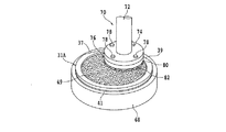
11 SiCインゴット
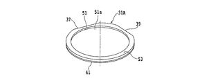
13,37 第一のオリエンテーションフラット
15,39 第二のオリエンテーションフラット
19 c軸
21 c面
30 レーザービーム照射ユニット
31 SiCウエーハ
36 集光器(レーザーヘッド)
41 保護テープ
43 改質層
45 クラック
47 環状溝
49 分離面
76 研削ホイール
82 研削砥石
Claims (2)
- 第一の面と、該第一の面と反対側の第二の面と、該第一の面から該第二の面に至るc軸と、該c軸に直交するc面とを有するSiC基板の該第一の面に複数のデバイスが形成されたデバイス領域と該デバイス領域を囲繞する外周余剰領域とを備えたウエーハを薄化するウエーハの薄化方法であって、
該デバイス領域と該外周余剰領域との境界部に対応する該第二の面に薄化されたウエーハの仕上がり厚みに相当する厚みを残して環状溝を形成する環状溝形成ステップと、
SiC基板に対して透過性を有する波長のレーザービームの集光点を該第二の面からウエーハの仕上がり厚みに相当する位置に位置付けると共に、該集光点とSiC基板とを相対的に移動してレーザービームを該第二の面に照射し、該環状溝に囲繞されたウエーハの仕上がり厚みに相当する位置に改質層及びクラックを形成して分離起点とする分離起点形成ステップと、
該分離起点形成ステップを実施した後、外力を付与して該分離起点から該第二の面を有するウエーハを複数のデバイスが形成された該第一の面を有するウエーハから分離して、該第一の面を有するウエーハを薄化すると共に該外周余剰領域に対応する位置にリング状の補強部を形成するウエーハ薄化ステップと、を備え、
該分離起点形成ステップは、該第二の面の垂線に対して該c軸がオフ角分傾き、該第二の面と該c面との間にオフ角が形成される方向と直交する方向にレーザービームの集光点を相対的に移動して直線状の改質層を形成する改質層形成ステップと、
該オフ角が形成される方向に該集光点を相対的に移動して所定量インデックスするインデックスステップと、を含むことを特徴とするウエーハの薄化方法。 - 該ウエーハ薄化ステップを実施した後、複数のデバイスが形成された該第一の面を有するウエーハの裏面を研削して平坦化する研削ステップを更に備えた請求項1記載のウエーハの薄化方法。
Priority Applications (8)
| Application Number | Priority Date | Filing Date | Title |
|---|---|---|---|
| JP2015144350A JP6482425B2 (ja) | 2015-07-21 | 2015-07-21 | ウエーハの薄化方法 |
| TW105119574A TWI696539B (zh) | 2015-07-21 | 2016-06-22 | 晶圓之薄化方法 |
| SG10201605424SA SG10201605424SA (en) | 2015-07-21 | 2016-07-01 | Wafer thinning method |
| MYPI2016702449A MY177495A (en) | 2015-07-21 | 2016-07-01 | Wafer thinning method |
| KR1020160086188A KR102419485B1 (ko) | 2015-07-21 | 2016-07-07 | 웨이퍼의 박화 방법 |
| US15/209,292 US10319593B2 (en) | 2015-07-21 | 2016-07-13 | Wafer thinning method |
| CN201610569364.0A CN106363824B (zh) | 2015-07-21 | 2016-07-19 | 晶片的薄化方法 |
| DE102016213249.0A DE102016213249A1 (de) | 2015-07-21 | 2016-07-20 | Verfahren zum dünnen Ausgestalten eines Wafers |
Applications Claiming Priority (1)
| Application Number | Priority Date | Filing Date | Title |
|---|---|---|---|
| JP2015144350A JP6482425B2 (ja) | 2015-07-21 | 2015-07-21 | ウエーハの薄化方法 |
Publications (2)
| Publication Number | Publication Date |
|---|---|
| JP2017024039A JP2017024039A (ja) | 2017-02-02 |
| JP6482425B2 true JP6482425B2 (ja) | 2019-03-13 |
Family
ID=57739022
Family Applications (1)
| Application Number | Title | Priority Date | Filing Date |
|---|---|---|---|
| JP2015144350A Active JP6482425B2 (ja) | 2015-07-21 | 2015-07-21 | ウエーハの薄化方法 |
Country Status (8)
| Country | Link |
|---|---|
| US (1) | US10319593B2 (ja) |
| JP (1) | JP6482425B2 (ja) |
| KR (1) | KR102419485B1 (ja) |
| CN (1) | CN106363824B (ja) |
| DE (1) | DE102016213249A1 (ja) |
| MY (1) | MY177495A (ja) |
| SG (1) | SG10201605424SA (ja) |
| TW (1) | TWI696539B (ja) |
Families Citing this family (35)
| Publication number | Priority date | Publication date | Assignee | Title |
|---|---|---|---|---|
| JP6478821B2 (ja) * | 2015-06-05 | 2019-03-06 | 株式会社ディスコ | ウエーハの生成方法 |
| DE102016116241A1 (de) * | 2016-08-31 | 2018-03-01 | Infineon Technologies Ag | Verfahren zum bearbeiten eines wafers und verfahren zum bearbeiten eines trägers |
| JP6914587B2 (ja) * | 2017-05-25 | 2021-08-04 | 株式会社ディスコ | ウェーハの加工方法 |
| CN111095493B (zh) * | 2017-09-04 | 2024-04-02 | 琳得科株式会社 | 薄型化板状部件的制造方法以及薄型化板状部件的制造装置 |
| US10388526B1 (en) | 2018-04-20 | 2019-08-20 | Semiconductor Components Industries, Llc | Semiconductor wafer thinning systems and related methods |
| US10896815B2 (en) | 2018-05-22 | 2021-01-19 | Semiconductor Components Industries, Llc | Semiconductor substrate singulation systems and related methods |
| US11121035B2 (en) | 2018-05-22 | 2021-09-14 | Semiconductor Components Industries, Llc | Semiconductor substrate processing methods |
| US20190363018A1 (en) | 2018-05-24 | 2019-11-28 | Semiconductor Components Industries, Llc | Die cleaning systems and related methods |
| US11830771B2 (en) | 2018-05-31 | 2023-11-28 | Semiconductor Components Industries, Llc | Semiconductor substrate production systems and related methods |
| US10468304B1 (en) | 2018-05-31 | 2019-11-05 | Semiconductor Components Industries, Llc | Semiconductor substrate production systems and related methods |
| CN118983257A (zh) | 2018-07-19 | 2024-11-19 | 东京毅力科创株式会社 | 基板处理装置和基板处理方法 |
| KR102745886B1 (ko) | 2018-12-21 | 2024-12-23 | 도쿄엘렉트론가부시키가이샤 | 기판 처리 장치 및 기판 처리 방법 |
| CN113195152B (zh) | 2018-12-21 | 2023-05-05 | 东京毅力科创株式会社 | 基板处理装置和基板处理方法 |
| KR20250130438A (ko) | 2018-12-21 | 2025-09-01 | 도쿄엘렉트론가부시키가이샤 | 기판 처리 방법 및 기판 처리 장치 |
| US11024501B2 (en) | 2018-12-29 | 2021-06-01 | Cree, Inc. | Carrier-assisted method for parting crystalline material along laser damage region |
| US10562130B1 (en) | 2018-12-29 | 2020-02-18 | Cree, Inc. | Laser-assisted method for parting crystalline material |
| US10576585B1 (en) | 2018-12-29 | 2020-03-03 | Cree, Inc. | Laser-assisted method for parting crystalline material |
| TWI816968B (zh) | 2019-01-23 | 2023-10-01 | 日商東京威力科創股份有限公司 | 基板處理裝置及基板處理方法 |
| CN109979808B (zh) * | 2019-03-14 | 2021-04-06 | 北京大学深圳研究生院 | 一种减薄碳化硅片的方法、装置及其应用 |
| TWI870391B (zh) | 2019-03-28 | 2025-01-21 | 日商東京威力科創股份有限公司 | 處理裝置及處理方法 |
| KR20250078630A (ko) | 2019-04-19 | 2025-06-02 | 도쿄엘렉트론가부시키가이샤 | 기판 처리 장치 및 기판 처리 방법 |
| US10611052B1 (en) | 2019-05-17 | 2020-04-07 | Cree, Inc. | Silicon carbide wafers with relaxed positive bow and related methods |
| US20220223475A1 (en) * | 2019-05-23 | 2022-07-14 | Tokyo Electron Limited | Substrate processing method and substrate processing system |
| TWI877184B (zh) * | 2019-07-18 | 2025-03-21 | 日商東京威力科創股份有限公司 | 處理裝置及處理方法 |
| JP7266953B2 (ja) * | 2019-08-07 | 2023-05-01 | 株式会社ディスコ | 保護部材形成方法及び保護部材形成装置 |
| JP7412131B2 (ja) * | 2019-10-28 | 2024-01-12 | 東京エレクトロン株式会社 | 基板処理方法及び基板処理システム |
| JP7386075B2 (ja) * | 2019-12-25 | 2023-11-24 | 東京エレクトロン株式会社 | 基板処理方法及び基板処理システム |
| US20220020705A1 (en) | 2020-07-20 | 2022-01-20 | Western Digital Technologies, Inc. | Semiconductor wafer thinned by stealth lasing |
| JP7680195B2 (ja) * | 2020-09-25 | 2025-05-20 | 株式会社ディスコ | ウエーハの分離方法 |
| CN117182290A (zh) * | 2022-06-01 | 2023-12-08 | 华为数字能源技术有限公司 | 激光加工设备、加工方法以及晶圆薄片 |
| US12506015B2 (en) | 2022-06-15 | 2025-12-23 | SanDisk Technologies, Inc. | Semiconductor wafer thinned by horizontal stealth lasing |
| CN116727901A (zh) * | 2023-06-29 | 2023-09-12 | 重庆伟特森电子科技有限公司 | 一种激光隐切制备Taiko碳化硅晶圆的方法 |
| US12438001B1 (en) * | 2024-04-05 | 2025-10-07 | Wolfspeed, Inc. | Off axis laser-based surface processing operations for semiconductor wafers |
| US12269123B1 (en) | 2024-04-05 | 2025-04-08 | Wolfspeed, Inc. | Laser edge shaping for semiconductor wafers |
| US12434330B1 (en) | 2024-04-05 | 2025-10-07 | Wolfspeed, Inc. | Laser-based surface processing for semiconductor workpiece |
Family Cites Families (85)
| Publication number | Priority date | Publication date | Assignee | Title |
|---|---|---|---|---|
| US5223692A (en) | 1991-09-23 | 1993-06-29 | General Electric Company | Method and apparatus for laser trepanning |
| FR2716303B1 (fr) | 1994-02-11 | 1996-04-05 | Franck Delorme | Laser à réflecteurs de Bragg distribués, accordable en longueur d'onde, à réseaux de diffraction virtuels activés sélectivement. |
| US5561544A (en) | 1995-03-06 | 1996-10-01 | Macken; John A. | Laser scanning system with reflecting optics |
| TW350095B (en) | 1995-11-21 | 1999-01-11 | Daido Hoxan Inc | Cutting method and apparatus for semiconductor materials |
| US6146979A (en) * | 1997-05-12 | 2000-11-14 | Silicon Genesis Corporation | Pressurized microbubble thin film separation process using a reusable substrate |
| JP2000094221A (ja) | 1998-09-24 | 2000-04-04 | Toyo Advanced Technologies Co Ltd | 放電式ワイヤソー |
| JP4659300B2 (ja) | 2000-09-13 | 2011-03-30 | 浜松ホトニクス株式会社 | レーザ加工方法及び半導体チップの製造方法 |
| US6720522B2 (en) | 2000-10-26 | 2004-04-13 | Kabushiki Kaisha Toshiba | Apparatus and method for laser beam machining, and method for manufacturing semiconductor devices using laser beam machining |
| JP4731050B2 (ja) | 2001-06-15 | 2011-07-20 | 株式会社ディスコ | 半導体ウエーハの加工方法 |
| TWI261358B (en) | 2002-01-28 | 2006-09-01 | Semiconductor Energy Lab | Semiconductor device and method of manufacturing the same |
| CN101335235B (zh) | 2002-03-12 | 2010-10-13 | 浜松光子学株式会社 | 基板的分割方法 |
| US6992765B2 (en) | 2002-10-11 | 2006-01-31 | Intralase Corp. | Method and system for determining the alignment of a surface of a material in relation to a laser beam |
| TWI520269B (zh) | 2002-12-03 | 2016-02-01 | 濱松赫德尼古斯股份有限公司 | Cutting method of semiconductor substrate |
| US7427555B2 (en) | 2002-12-16 | 2008-09-23 | The Regents Of The University Of California | Growth of planar, non-polar gallium nitride by hydride vapor phase epitaxy |
| US20040144301A1 (en) | 2003-01-24 | 2004-07-29 | Neudeck Philip G. | Method for growth of bulk crystals by vapor phase epitaxy |
| JP2005268752A (ja) | 2004-02-19 | 2005-09-29 | Canon Inc | レーザ割断方法、被割断部材および半導体素子チップ |
| US20050217560A1 (en) | 2004-03-31 | 2005-10-06 | Tolchinsky Peter G | Semiconductor wafers with non-standard crystal orientations and methods of manufacturing the same |
| US20080070380A1 (en) | 2004-06-11 | 2008-03-20 | Showda Denko K.K. | Production Method of Compound Semiconductor Device Wafer |
| JP2006108532A (ja) * | 2004-10-08 | 2006-04-20 | Disco Abrasive Syst Ltd | ウエーハの研削方法 |
| JP2006187783A (ja) | 2005-01-05 | 2006-07-20 | Disco Abrasive Syst Ltd | レーザー加工装置 |
| JP2006315017A (ja) | 2005-05-11 | 2006-11-24 | Canon Inc | レーザ切断方法および被切断部材 |
| JP4809632B2 (ja) | 2005-06-01 | 2011-11-09 | ルネサスエレクトロニクス株式会社 | 半導体装置の製造方法 |
| JP2007019379A (ja) | 2005-07-11 | 2007-01-25 | Disco Abrasive Syst Ltd | ウェーハの加工方法 |
| JP4749799B2 (ja) | 2005-08-12 | 2011-08-17 | 浜松ホトニクス株式会社 | レーザ加工方法 |
| US9138913B2 (en) | 2005-09-08 | 2015-09-22 | Imra America, Inc. | Transparent material processing with an ultrashort pulse laser |
| JP4183093B2 (ja) | 2005-09-12 | 2008-11-19 | コバレントマテリアル株式会社 | シリコンウエハの製造方法 |
| WO2007055010A1 (ja) | 2005-11-10 | 2007-05-18 | Renesas Technology Corp. | 半導体装置の製造方法および半導体装置 |
| US20070111480A1 (en) | 2005-11-16 | 2007-05-17 | Denso Corporation | Wafer product and processing method therefor |
| US8835802B2 (en) | 2006-01-24 | 2014-09-16 | Stephen C. Baer | Cleaving wafers from silicon crystals |
| JP5073962B2 (ja) * | 2006-05-12 | 2012-11-14 | 株式会社ディスコ | ウエーハの加工方法 |
| JP2007329391A (ja) * | 2006-06-09 | 2007-12-20 | Disco Abrasive Syst Ltd | 半導体ウェーハの結晶方位指示マーク検出機構 |
| US8980445B2 (en) | 2006-07-06 | 2015-03-17 | Cree, Inc. | One hundred millimeter SiC crystal grown on off-axis seed |
| TW200827600A (en) * | 2006-12-22 | 2008-07-01 | Jin-Fa Yan | The leakage prevention method of a hydraulic magnetron |
| JP2008283025A (ja) * | 2007-05-11 | 2008-11-20 | Disco Abrasive Syst Ltd | ウエーハの分割方法 |
| EP2009687B1 (en) * | 2007-06-29 | 2016-08-17 | Semiconductor Energy Laboratory Co., Ltd. | Method of manufacturing an SOI substrate and method of manufacturing a semiconductor device |
| JP2009061462A (ja) * | 2007-09-05 | 2009-03-26 | Sumitomo Electric Ind Ltd | 基板の製造方法および基板 |
| JP5011072B2 (ja) | 2007-11-21 | 2012-08-29 | 株式会社ディスコ | レーザー加工装置 |
| US8338218B2 (en) | 2008-06-26 | 2012-12-25 | Semiconductor Energy Laboratory Co., Ltd. | Photoelectric conversion device module and manufacturing method of the photoelectric conversion device module |
| JP2010021398A (ja) | 2008-07-11 | 2010-01-28 | Disco Abrasive Syst Ltd | ウェーハの処理方法 |
| JP5692969B2 (ja) | 2008-09-01 | 2015-04-01 | 浜松ホトニクス株式会社 | 収差補正方法、この収差補正方法を用いたレーザ加工方法、この収差補正方法を用いたレーザ照射方法、収差補正装置、及び、収差補正プログラム |
| JP5601778B2 (ja) * | 2009-02-19 | 2014-10-08 | 信越ポリマー株式会社 | 半導体ウェーハの製造方法 |
| BR122019015544B1 (pt) | 2009-02-25 | 2020-12-22 | Nichia Corporation | método para fabricar um elemento semicondutor, e, elemento semicondutor |
| WO2010123976A1 (en) | 2009-04-21 | 2010-10-28 | Tetrasun, Inc. | Method for forming structures in a solar cell |
| JP5537081B2 (ja) | 2009-07-28 | 2014-07-02 | 浜松ホトニクス株式会社 | 加工対象物切断方法 |
| JP5379604B2 (ja) | 2009-08-21 | 2013-12-25 | 浜松ホトニクス株式会社 | レーザ加工方法及びチップ |
| JP5558128B2 (ja) | 2010-02-05 | 2014-07-23 | 株式会社ディスコ | 光デバイスウエーハの加工方法 |
| JP2011165766A (ja) | 2010-02-05 | 2011-08-25 | Disco Abrasive Syst Ltd | 光デバイスウエーハの加工方法 |
| JP5370262B2 (ja) | 2010-05-18 | 2013-12-18 | 豊田合成株式会社 | 半導体発光チップおよび基板の加工方法 |
| US8722516B2 (en) | 2010-09-28 | 2014-05-13 | Hamamatsu Photonics K.K. | Laser processing method and method for manufacturing light-emitting device |
| RU2459691C2 (ru) * | 2010-11-29 | 2012-08-27 | Юрий Георгиевич Шретер | Способ отделения поверхностного слоя полупроводникового кристалла (варианты) |
| JP5480169B2 (ja) | 2011-01-13 | 2014-04-23 | 浜松ホトニクス株式会社 | レーザ加工方法 |
| JP5904720B2 (ja) | 2011-05-12 | 2016-04-20 | 株式会社ディスコ | ウエーハの分割方法 |
| JP5912287B2 (ja) | 2011-05-19 | 2016-04-27 | 株式会社ディスコ | レーザー加工方法およびレーザー加工装置 |
| JP5912293B2 (ja) | 2011-05-24 | 2016-04-27 | 株式会社ディスコ | レーザー加工装置 |
| JP5917862B2 (ja) | 2011-08-30 | 2016-05-18 | 浜松ホトニクス株式会社 | 加工対象物切断方法 |
| KR20130026810A (ko) * | 2011-09-06 | 2013-03-14 | 주식회사 이오테크닉스 | 레이저 가공 방법 |
| JP5878330B2 (ja) | 2011-10-18 | 2016-03-08 | 株式会社ディスコ | レーザー光線の出力設定方法およびレーザー加工装置 |
| TWI509709B (zh) * | 2011-11-08 | 2015-11-21 | United Microelectronics Corp | 半導體結構之製作方法 |
| US8747982B2 (en) | 2011-12-28 | 2014-06-10 | Sicrystal Aktiengesellschaft | Production method for an SiC volume monocrystal with a homogeneous lattice plane course and a monocrystalline SiC substrate with a homogeneous lattice plane course |
| US9214353B2 (en) * | 2012-02-26 | 2015-12-15 | Solexel, Inc. | Systems and methods for laser splitting and device layer transfer |
| JP6004705B2 (ja) * | 2012-04-02 | 2016-10-12 | 株式会社ディスコ | 接着フィルム付きチップの形成方法 |
| JP2014041924A (ja) | 2012-08-22 | 2014-03-06 | Hamamatsu Photonics Kk | 加工対象物切断方法 |
| US9093566B2 (en) * | 2012-12-31 | 2015-07-28 | Taiwan Semiconductor Manufacturing Company, Ltd. | High efficiency FinFET diode |
| JP6090998B2 (ja) | 2013-01-31 | 2017-03-08 | 一般財団法人電力中央研究所 | 六方晶単結晶の製造方法、六方晶単結晶ウエハの製造方法 |
| US9768343B2 (en) | 2013-04-29 | 2017-09-19 | OB Realty, LLC. | Damage free laser patterning of transparent layers for forming doped regions on a solar cell substrate |
| JP6341639B2 (ja) * | 2013-08-01 | 2018-06-13 | 株式会社ディスコ | 加工装置 |
| US20150121960A1 (en) | 2013-11-04 | 2015-05-07 | Rofin-Sinar Technologies Inc. | Method and apparatus for machining diamonds and gemstones using filamentation by burst ultrafast laser pulses |
| US9850160B2 (en) | 2013-12-17 | 2017-12-26 | Corning Incorporated | Laser cutting of display glass compositions |
| JP2015119076A (ja) * | 2013-12-19 | 2015-06-25 | 信越ポリマー株式会社 | 内部加工層形成単結晶部材およびその製造方法 |
| US9757815B2 (en) | 2014-07-21 | 2017-09-12 | Rofin-Sinar Technologies Inc. | Method and apparatus for performing laser curved filamentation within transparent materials |
| JP6390898B2 (ja) | 2014-08-22 | 2018-09-19 | アイシン精機株式会社 | 基板の製造方法、加工対象物の切断方法、及び、レーザ加工装置 |
| RU2674916C2 (ru) | 2014-10-13 | 2018-12-14 | Эвана Текнолоджис, Уаб | Способ лазерной обработки для разделения или скрайбирования подложки путем формирования клиновидных поврежденных структур |
| US10307867B2 (en) | 2014-11-05 | 2019-06-04 | Asm Technology Singapore Pte Ltd | Laser fiber array for singulating semiconductor wafers |
| JP6358941B2 (ja) | 2014-12-04 | 2018-07-18 | 株式会社ディスコ | ウエーハの生成方法 |
| JP5917677B1 (ja) * | 2014-12-26 | 2016-05-18 | エルシード株式会社 | SiC材料の加工方法 |
| JP6395613B2 (ja) | 2015-01-06 | 2018-09-26 | 株式会社ディスコ | ウエーハの生成方法 |
| JP6395633B2 (ja) | 2015-02-09 | 2018-09-26 | 株式会社ディスコ | ウエーハの生成方法 |
| JP6395634B2 (ja) | 2015-02-09 | 2018-09-26 | 株式会社ディスコ | ウエーハの生成方法 |
| JP6425606B2 (ja) | 2015-04-06 | 2018-11-21 | 株式会社ディスコ | ウエーハの生成方法 |
| JP6482389B2 (ja) | 2015-06-02 | 2019-03-13 | 株式会社ディスコ | ウエーハの生成方法 |
| JP6472333B2 (ja) | 2015-06-02 | 2019-02-20 | 株式会社ディスコ | ウエーハの生成方法 |
| JP6482423B2 (ja) | 2015-07-16 | 2019-03-13 | 株式会社ディスコ | ウエーハの生成方法 |
| JP6486239B2 (ja) | 2015-08-18 | 2019-03-20 | 株式会社ディスコ | ウエーハの加工方法 |
| JP6486240B2 (ja) | 2015-08-18 | 2019-03-20 | 株式会社ディスコ | ウエーハの加工方法 |
| JP6602207B2 (ja) | 2016-01-07 | 2019-11-06 | 株式会社ディスコ | SiCウエーハの生成方法 |
-
2015
- 2015-07-21 JP JP2015144350A patent/JP6482425B2/ja active Active
-
2016
- 2016-06-22 TW TW105119574A patent/TWI696539B/zh active
- 2016-07-01 MY MYPI2016702449A patent/MY177495A/en unknown
- 2016-07-01 SG SG10201605424SA patent/SG10201605424SA/en unknown
- 2016-07-07 KR KR1020160086188A patent/KR102419485B1/ko active Active
- 2016-07-13 US US15/209,292 patent/US10319593B2/en active Active
- 2016-07-19 CN CN201610569364.0A patent/CN106363824B/zh active Active
- 2016-07-20 DE DE102016213249.0A patent/DE102016213249A1/de active Pending
Also Published As
| Publication number | Publication date |
|---|---|
| KR102419485B1 (ko) | 2022-07-08 |
| KR20170012025A (ko) | 2017-02-02 |
| SG10201605424SA (en) | 2017-02-27 |
| US20170025275A1 (en) | 2017-01-26 |
| US10319593B2 (en) | 2019-06-11 |
| TWI696539B (zh) | 2020-06-21 |
| JP2017024039A (ja) | 2017-02-02 |
| MY177495A (en) | 2020-09-16 |
| TW201722668A (zh) | 2017-07-01 |
| CN106363824A (zh) | 2017-02-01 |
| CN106363824B (zh) | 2019-11-29 |
| DE102016213249A1 (de) | 2017-01-26 |
Similar Documents
| Publication | Publication Date | Title |
|---|---|---|
| JP6482425B2 (ja) | ウエーハの薄化方法 | |
| JP6472347B2 (ja) | ウエーハの薄化方法 | |
| JP6486239B2 (ja) | ウエーハの加工方法 | |
| JP6486240B2 (ja) | ウエーハの加工方法 | |
| JP6562819B2 (ja) | SiC基板の分離方法 | |
| JP6456228B2 (ja) | 薄板の分離方法 | |
| JP6444249B2 (ja) | ウエーハの生成方法 | |
| JP6358941B2 (ja) | ウエーハの生成方法 | |
| JP6355540B2 (ja) | ウエーハの生成方法 | |
| JP2014099522A (ja) | 板状物の加工方法 |
Legal Events
| Date | Code | Title | Description |
|---|---|---|---|
| A621 | Written request for application examination |
Free format text: JAPANESE INTERMEDIATE CODE: A621 Effective date: 20180515 |
|
| A977 | Report on retrieval |
Free format text: JAPANESE INTERMEDIATE CODE: A971007 Effective date: 20190124 |
|
| TRDD | Decision of grant or rejection written | ||
| A01 | Written decision to grant a patent or to grant a registration (utility model) |
Free format text: JAPANESE INTERMEDIATE CODE: A01 Effective date: 20190212 |
|
| A61 | First payment of annual fees (during grant procedure) |
Free format text: JAPANESE INTERMEDIATE CODE: A61 Effective date: 20190212 |
|
| R150 | Certificate of patent or registration of utility model |
Ref document number: 6482425 Country of ref document: JP Free format text: JAPANESE INTERMEDIATE CODE: R150 |
|
| R250 | Receipt of annual fees |
Free format text: JAPANESE INTERMEDIATE CODE: R250 |
|
| R250 | Receipt of annual fees |
Free format text: JAPANESE INTERMEDIATE CODE: R250 |
|
| R250 | Receipt of annual fees |
Free format text: JAPANESE INTERMEDIATE CODE: R250 |
|
| R250 | Receipt of annual fees |
Free format text: JAPANESE INTERMEDIATE CODE: R250 |
|
| R250 | Receipt of annual fees |
Free format text: JAPANESE INTERMEDIATE CODE: R250 |