JP6404591B2 - 半導体装置の製造方法、半導体装置の評価方法および半導体装置 - Google Patents
半導体装置の製造方法、半導体装置の評価方法および半導体装置 Download PDFInfo
- Publication number
- JP6404591B2 JP6404591B2 JP2014089124A JP2014089124A JP6404591B2 JP 6404591 B2 JP6404591 B2 JP 6404591B2 JP 2014089124 A JP2014089124 A JP 2014089124A JP 2014089124 A JP2014089124 A JP 2014089124A JP 6404591 B2 JP6404591 B2 JP 6404591B2
- Authority
- JP
- Japan
- Prior art keywords
- electrode
- gate
- screening
- trench
- pad
- Prior art date
- Legal status (The legal status is an assumption and is not a legal conclusion. Google has not performed a legal analysis and makes no representation as to the accuracy of the status listed.)
- Active
Links
Images


Classifications
-
- H—ELECTRICITY
- H10—SEMICONDUCTOR DEVICES; ELECTRIC SOLID-STATE DEVICES NOT OTHERWISE PROVIDED FOR
- H10D—INORGANIC ELECTRIC SEMICONDUCTOR DEVICES
- H10D62/00—Semiconductor bodies, or regions thereof, of devices having potential barriers
- H10D62/10—Shapes, relative sizes or dispositions of the regions of the semiconductor bodies; Shapes of the semiconductor bodies
- H10D62/124—Shapes, relative sizes or dispositions of the regions of semiconductor bodies or of junctions between the regions
- H10D62/126—Top-view geometrical layouts of the regions or the junctions
- H10D62/127—Top-view geometrical layouts of the regions or the junctions of cellular field-effect devices, e.g. multicellular DMOS transistors or IGBTs
-
- H—ELECTRICITY
- H10—SEMICONDUCTOR DEVICES; ELECTRIC SOLID-STATE DEVICES NOT OTHERWISE PROVIDED FOR
- H10D—INORGANIC ELECTRIC SEMICONDUCTOR DEVICES
- H10D64/00—Electrodes of devices having potential barriers
- H10D64/01—Manufacture or treatment
- H10D64/017—Manufacture or treatment using dummy gates in processes wherein at least parts of the final gates are self-aligned to the dummy gates, i.e. replacement gate processes
-
- G—PHYSICS
- G01—MEASURING; TESTING
- G01R—MEASURING ELECTRIC VARIABLES; MEASURING MAGNETIC VARIABLES
- G01R31/00—Arrangements for testing electric properties; Arrangements for locating electric faults; Arrangements for electrical testing characterised by what is being tested not provided for elsewhere
- G01R31/26—Testing of individual semiconductor devices
- G01R31/2601—Apparatus or methods therefor
-
- H—ELECTRICITY
- H10—SEMICONDUCTOR DEVICES; ELECTRIC SOLID-STATE DEVICES NOT OTHERWISE PROVIDED FOR
- H10D—INORGANIC ELECTRIC SEMICONDUCTOR DEVICES
- H10D12/00—Bipolar devices controlled by the field effect, e.g. insulated-gate bipolar transistors [IGBT]
- H10D12/01—Manufacture or treatment
- H10D12/031—Manufacture or treatment of IGBTs
- H10D12/032—Manufacture or treatment of IGBTs of vertical IGBTs
- H10D12/038—Manufacture or treatment of IGBTs of vertical IGBTs having a recessed gate, e.g. trench-gate IGBTs
-
- H—ELECTRICITY
- H10—SEMICONDUCTOR DEVICES; ELECTRIC SOLID-STATE DEVICES NOT OTHERWISE PROVIDED FOR
- H10D—INORGANIC ELECTRIC SEMICONDUCTOR DEVICES
- H10D12/00—Bipolar devices controlled by the field effect, e.g. insulated-gate bipolar transistors [IGBT]
- H10D12/411—Insulated-gate bipolar transistors [IGBT]
- H10D12/441—Vertical IGBTs
- H10D12/461—Vertical IGBTs having non-planar surfaces, e.g. having trenches, recesses or pillars in the surfaces of the emitter, base or collector regions
- H10D12/481—Vertical IGBTs having non-planar surfaces, e.g. having trenches, recesses or pillars in the surfaces of the emitter, base or collector regions having gate structures on slanted surfaces, on vertical surfaces, or in grooves, e.g. trench gate IGBTs
-
- H—ELECTRICITY
- H10—SEMICONDUCTOR DEVICES; ELECTRIC SOLID-STATE DEVICES NOT OTHERWISE PROVIDED FOR
- H10D—INORGANIC ELECTRIC SEMICONDUCTOR DEVICES
- H10D62/00—Semiconductor bodies, or regions thereof, of devices having potential barriers
- H10D62/10—Shapes, relative sizes or dispositions of the regions of the semiconductor bodies; Shapes of the semiconductor bodies
- H10D62/102—Constructional design considerations for preventing surface leakage or controlling electric field concentration
- H10D62/103—Constructional design considerations for preventing surface leakage or controlling electric field concentration for increasing or controlling the breakdown voltage of reverse-biased devices
- H10D62/105—Constructional design considerations for preventing surface leakage or controlling electric field concentration for increasing or controlling the breakdown voltage of reverse-biased devices by having particular doping profiles, shapes or arrangements of PN junctions; by having supplementary regions, e.g. junction termination extension [JTE]
- H10D62/106—Constructional design considerations for preventing surface leakage or controlling electric field concentration for increasing or controlling the breakdown voltage of reverse-biased devices by having particular doping profiles, shapes or arrangements of PN junctions; by having supplementary regions, e.g. junction termination extension [JTE] having supplementary regions doped oppositely to or in rectifying contact with regions of the semiconductor bodies, e.g. guard rings with PN or Schottky junctions
-
- H—ELECTRICITY
- H10—SEMICONDUCTOR DEVICES; ELECTRIC SOLID-STATE DEVICES NOT OTHERWISE PROVIDED FOR
- H10D—INORGANIC ELECTRIC SEMICONDUCTOR DEVICES
- H10D64/00—Electrodes of devices having potential barriers
- H10D64/01—Manufacture or treatment
- H10D64/018—Spacers formed inside holes at the prospective gate locations, e.g. holes left by removing dummy gates
-
- H—ELECTRICITY
- H10—SEMICONDUCTOR DEVICES; ELECTRIC SOLID-STATE DEVICES NOT OTHERWISE PROVIDED FOR
- H10D—INORGANIC ELECTRIC SEMICONDUCTOR DEVICES
- H10D64/00—Electrodes of devices having potential barriers
- H10D64/111—Field plates
- H10D64/117—Recessed field plates, e.g. trench field plates or buried field plates
-
- H—ELECTRICITY
- H10—SEMICONDUCTOR DEVICES; ELECTRIC SOLID-STATE DEVICES NOT OTHERWISE PROVIDED FOR
- H10D—INORGANIC ELECTRIC SEMICONDUCTOR DEVICES
- H10D64/00—Electrodes of devices having potential barriers
- H10D64/20—Electrodes characterised by their shapes, relative sizes or dispositions
- H10D64/27—Electrodes not carrying the current to be rectified, amplified, oscillated or switched, e.g. gates
- H10D64/311—Gate electrodes for field-effect devices
- H10D64/411—Gate electrodes for field-effect devices for FETs
- H10D64/511—Gate electrodes for field-effect devices for FETs for IGFETs
- H10D64/512—Disposition of the gate electrodes, e.g. buried gates
- H10D64/513—Disposition of the gate electrodes, e.g. buried gates within recesses in the substrate, e.g. trench gates, groove gates or buried gates
-
- H—ELECTRICITY
- H10—SEMICONDUCTOR DEVICES; ELECTRIC SOLID-STATE DEVICES NOT OTHERWISE PROVIDED FOR
- H10D—INORGANIC ELECTRIC SEMICONDUCTOR DEVICES
- H10D64/00—Electrodes of devices having potential barriers
- H10D64/20—Electrodes characterised by their shapes, relative sizes or dispositions
- H10D64/27—Electrodes not carrying the current to be rectified, amplified, oscillated or switched, e.g. gates
- H10D64/311—Gate electrodes for field-effect devices
- H10D64/411—Gate electrodes for field-effect devices for FETs
- H10D64/511—Gate electrodes for field-effect devices for FETs for IGFETs
- H10D64/517—Gate electrodes for field-effect devices for FETs for IGFETs characterised by the conducting layers
- H10D64/519—Gate electrodes for field-effect devices for FETs for IGFETs characterised by the conducting layers characterised by their top-view geometrical layouts
-
- H—ELECTRICITY
- H10—SEMICONDUCTOR DEVICES; ELECTRIC SOLID-STATE DEVICES NOT OTHERWISE PROVIDED FOR
- H10P—GENERIC PROCESSES OR APPARATUS FOR THE MANUFACTURE OR TREATMENT OF DEVICES COVERED BY CLASS H10
- H10P74/00—Testing or measuring during manufacture or treatment of wafers, substrates or devices
- H10P74/20—Testing or measuring during manufacture or treatment of wafers, substrates or devices characterised by the properties tested or measured, e.g. structural or electrical properties
- H10P74/207—Electrical properties, e.g. testing or measuring of resistance, deep levels or capacitance-voltage characteristics
-
- H—ELECTRICITY
- H10—SEMICONDUCTOR DEVICES; ELECTRIC SOLID-STATE DEVICES NOT OTHERWISE PROVIDED FOR
- H10P—GENERIC PROCESSES OR APPARATUS FOR THE MANUFACTURE OR TREATMENT OF DEVICES COVERED BY CLASS H10
- H10P74/00—Testing or measuring during manufacture or treatment of wafers, substrates or devices
- H10P74/27—Structural arrangements therefor
-
- H—ELECTRICITY
- H10—SEMICONDUCTOR DEVICES; ELECTRIC SOLID-STATE DEVICES NOT OTHERWISE PROVIDED FOR
- H10W—GENERIC PACKAGES, INTERCONNECTIONS, CONNECTORS OR OTHER CONSTRUCTIONAL DETAILS OF DEVICES COVERED BY CLASS H10
- H10W72/00—Interconnections or connectors in packages
- H10W72/071—Connecting or disconnecting
- H10W72/075—Connecting or disconnecting of bond wires
- H10W72/07531—Techniques
- H10W72/07536—Soldering or alloying
-
- H—ELECTRICITY
- H10—SEMICONDUCTOR DEVICES; ELECTRIC SOLID-STATE DEVICES NOT OTHERWISE PROVIDED FOR
- H10W—GENERIC PACKAGES, INTERCONNECTIONS, CONNECTORS OR OTHER CONSTRUCTIONAL DETAILS OF DEVICES COVERED BY CLASS H10
- H10W72/00—Interconnections or connectors in packages
- H10W72/50—Bond wires
- H10W72/541—Dispositions of bond wires
- H10W72/5453—Dispositions of bond wires connecting between multiple bond pads on a chip, e.g. daisy chain
-
- H—ELECTRICITY
- H10—SEMICONDUCTOR DEVICES; ELECTRIC SOLID-STATE DEVICES NOT OTHERWISE PROVIDED FOR
- H10W—GENERIC PACKAGES, INTERCONNECTIONS, CONNECTORS OR OTHER CONSTRUCTIONAL DETAILS OF DEVICES COVERED BY CLASS H10
- H10W72/00—Interconnections or connectors in packages
- H10W72/50—Bond wires
- H10W72/541—Dispositions of bond wires
- H10W72/547—Dispositions of multiple bond wires
- H10W72/5473—Dispositions of multiple bond wires multiple bond wires connected to a common bond pad
-
- H—ELECTRICITY
- H10—SEMICONDUCTOR DEVICES; ELECTRIC SOLID-STATE DEVICES NOT OTHERWISE PROVIDED FOR
- H10W—GENERIC PACKAGES, INTERCONNECTIONS, CONNECTORS OR OTHER CONSTRUCTIONAL DETAILS OF DEVICES COVERED BY CLASS H10
- H10W72/00—Interconnections or connectors in packages
- H10W72/90—Bond pads, in general
- H10W72/921—Structures or relative sizes of bond pads
- H10W72/926—Multiple bond pads having different sizes
-
- H—ELECTRICITY
- H10—SEMICONDUCTOR DEVICES; ELECTRIC SOLID-STATE DEVICES NOT OTHERWISE PROVIDED FOR
- H10W—GENERIC PACKAGES, INTERCONNECTIONS, CONNECTORS OR OTHER CONSTRUCTIONAL DETAILS OF DEVICES COVERED BY CLASS H10
- H10W72/00—Interconnections or connectors in packages
- H10W72/90—Bond pads, in general
- H10W72/951—Materials of bond pads
- H10W72/952—Materials of bond pads comprising metals or metalloids, e.g. PbSn, Ag or Cu
-
- H—ELECTRICITY
- H10—SEMICONDUCTOR DEVICES; ELECTRIC SOLID-STATE DEVICES NOT OTHERWISE PROVIDED FOR
- H10W—GENERIC PACKAGES, INTERCONNECTIONS, CONNECTORS OR OTHER CONSTRUCTIONAL DETAILS OF DEVICES COVERED BY CLASS H10
- H10W90/00—Package configurations
- H10W90/701—Package configurations characterised by the relative positions of pads or connectors relative to package parts
- H10W90/751—Package configurations characterised by the relative positions of pads or connectors relative to package parts of bond wires
- H10W90/753—Package configurations characterised by the relative positions of pads or connectors relative to package parts of bond wires between laterally-adjacent chips
Landscapes
- Physics & Mathematics (AREA)
- General Physics & Mathematics (AREA)
- Testing Or Measuring Of Semiconductors Or The Like (AREA)
- Electrodes Of Semiconductors (AREA)
- Engineering & Computer Science (AREA)
- Manufacturing & Machinery (AREA)
- Internal Circuitry In Semiconductor Integrated Circuit Devices (AREA)
Description
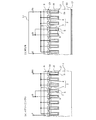
まず、実施の形態1にかかる半導体装置の製造方法により作製(製造)される半導体装置の一例としてトレンチゲート型IGBTの構造について説明する。図1は、実施の形態1にかかる半導体装置の製造方法により製造される半導体装置の一例を示す断面図である。図1(a)には、製造途中のスクリーニング時の状態を模式的に示す。図1(b)には、組立後の状態を模式的に示す。図1に示すように、実施の形態1にかかる半導体装置は、n-型ドリフト層となるn-型半導体基板(半導体チップ)1上に、トレンチ6側壁をチャネル領域(反転層)とするトレンチMOSセル(第1トレンチゲート構造)と、トレンチ(以下、ダミートレンチとする)16側壁にチャネル領域を形成しないトレンチMOSセル(以下、ダミートレンチMOSセル(第2トレンチゲート構造)とする)と、を備える。
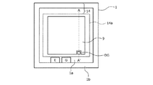
次に、実施の形態2にかかる半導体装置の製造方法によって作製される半導体装置の構造について説明する。図6は、実施の形態2にかかる半導体装置の各電極パッドの平面レイアウトを示す平面図である。図6の切断線A−A’における断面構造は、実施の形態1(図4)と同様である。図7は、実施の形態2にかかる半導体装置の各電極パッドの別の一例の平面レイアウトを示す平面図である。図8は、図6のスクリーニングパッド付近を拡大して示す平面図である。実施の形態2にかかる半導体装置の製造方法によって作製される半導体装置が実施の形態1にかかる半導体装置の製造方法によって作製される半導体装置と異なる点は、スクリーニングパッドDGの周囲2辺以上がエミッタ電極9に対向する点である。
次に、実施の形態3にかかる半導体装置の製造方法について説明する。図9は、実施の形態3にかかる半導体装置の製造方法の概要を示すフローチャートである。図10は、実施の形態3にかかる半導体装置の各電極パッドの平面レイアウトを示す平面図である。実施の形態3にかかる半導体装置の製造方法が実施の形態1にかかる半導体装置の製造方法と異なる点は、次の2点である。1つ目の相違点は、ゲート絶縁膜7およびダミーゲート絶縁膜17に対するスクリーニングをウエハ検査時に行う点である。2つ目の相違点は、組立工程におけるワイヤーボンディングにより、エミッタ電極9とスクリーニングパッドDGとを短絡させる点である。
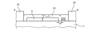
次に、実施の形態4にかかる半導体装置の製造方法について説明する。図11は、実施の形態4にかかる半導体装置の製造方法の概要を示すフローチャートである。図12は、実施の形態4にかかる半導体装置の各電極パッドの平面レイアウトを示す平面図である。図13は、図12の切断線B−B’における断面構造を示す断面図である。実施の形態4にかかる半導体装置の製造方法が実施の形態3にかかる半導体装置の製造方法と異なる点は、組立工程における銅ブロック19へのチップおもて面の半田付けにより、エミッタ電極9とスクリーニングパッドDGとを短絡させる点である。
次に、実施の形態5にかかる半導体装置の製造方法について、図5を参照しながら説明する。実施の形態5にかかる半導体装置の製造方法が実施の形態1にかかる半導体装置の製造方法と異なる点は、一旦、すべてのトレンチゲート構造をトレンチMOSセルとして形成し(すなわち、n-型半導体基板に形成したすべてのトレンチゲート構造をすべてゲート電極8としてゲートランナーに接続し)、すべてのゲート絶縁膜7を一括してスクリーニングした後に、ゲートランナーに接続された一部のゲート電極8を電気的に切り離してダミーゲート電極18にする点である。
1a 活性領域
1b エッジ終端領域
2 p型ベース層
3 第1ベース領域
4 第2ベース領域
5 n+型エミッタ領域
6 トレンチ
7 ゲート絶縁膜
8 ゲート電極
9 エミッタ電極
10 層間絶縁膜
11 p+型コレクタ層
12 コレクタ電極
13 めっき膜
14 おもて面保護膜
14a おもて面保護膜の内終端
15 半田層
16 ダミートレンチ
17 ダミーゲート絶縁膜
18 ダミーゲート電極
19 銅ブロック
DG スクリーニングパッド
E エミッタパッド
G ゲートパッド
w エミッタ電極とスクリーニングパッドとの間隔
Claims (8)
- 素子の深さ方向に延びるゲート電極を備えたトレンチゲート構造を複数備え、複数の前記トレンチゲート構造が、素子の制御に寄与する第1トレンチゲート構造と、素子の制御に寄与しない第2トレンチゲート構造とからなる半導体装置の製造方法であって、
半導体基板のおもて面側に、複数の前記トレンチゲート構造を形成する第1工程と、
前記半導体基板のおもて面上に、複数の前記トレンチゲート構造のすべての前記ゲート電極が同一の配線によってすべて接続されたゲート電極パッドを形成する第2工程と、
ゲート電位以外の電位をもつ電極部と前記ゲート電極パッドとの間に所定電圧を印加して、前記ゲート電極パッドに接続された前記ゲート電極に接するゲート絶縁膜に前記所定電圧を印加するスクリーニングを行う第3工程と、
前記第3工程の後、前記配線から一部の前記ゲート電極を電気的に切り離し、前記切り離された前記ゲート電極を前記ゲート電極パッドとは異なるスクリーニング電極パッドに接続する第4工程と、
前記第4工程の後、前記電極部と、前記切り離された前記ゲート電極が接続された前記スクリーニング電極パッドとを短絡させて、前記切り離された前記ゲート電極を備えた前記第2トレンチゲート構造を形成する第5工程と、
を含むことを特徴とする半導体装置の製造方法。 - 前記第5工程では、
前記電極部、および前記第2トレンチゲート構造の前記ゲート電極が接続された前記スクリーニング電極パッドを覆うめっき膜を形成し、
前記電極部と、前記第2トレンチゲート構造の前記ゲート電極が接続された前記スクリーニング電極パッドとの間に広がった前記めっき膜を介して、前記電極部と、前記第2トレンチゲート構造の前記ゲート電極が接続された前記スクリーニング電極パッドとを接続することを特徴とする請求項1に記載の半導体装置の製造方法。 - 前記第5工程は、
前記電極部の表面、および前記第2トレンチゲート構造の前記ゲート電極が接続された前記スクリーニング電極パッドの表面にめっき膜を形成する工程と、
前記めっき膜を介して前記電極部、および前記第2トレンチゲート構造の前記ゲート電極が接続された前記スクリーニング電極パッドに電極端子となる電極層を半田付けする工程と、を含み、
前記電極部と、前記第2トレンチゲート構造の前記ゲート電極が接続された前記スクリーニング電極パッドとの間に広がった半田層によって、前記電極部と、前記第2トレンチゲート構造の前記ゲート電極が接続された前記スクリーニング電極パッドとを接続することを特徴とする請求項1に記載の半導体装置の製造方法。 - 前記第5工程では、前記電極部と前記第1トレンチゲート構造の前記ゲート電極とにそれぞれワイヤーボンディングによる配線処理を行うとともに、ワイヤーボンディングにより前記電極部と、前記第2トレンチゲート構造の前記ゲート電極が接続された前記スクリーニング電極パッドとを接続することを特徴とする請求項1に記載の半導体装置の製造方法。
- 前記第4工程の後、前記第5工程の前に、前記電極部と前記第1トレンチゲート構造の前記ゲート電極とにそれぞれワイヤーボンディングによる配線処理を行い、
前記第5工程では、前記第2トレンチゲート構造の前記ゲート電極が接続された前記スクリーニング電極パッドを外部回路に設けられた前記電極部に接続することを特徴とする請求項1に記載の半導体装置の製造方法。 - 前記電極部は、前記半導体基板の、前記トレンチゲート構造のトレンチに沿った部分に電気的に接続されたエミッタ電極であることを特徴とする請求項1〜5のいずれか一つに記載の半導体装置の製造方法。
- 半導体基板のおもて面側に、素子の深さ方向に伸びるゲート電極を備えた複数のトレンチゲート構造を備えた半導体装置であって、
複数の前記トレンチゲート構造のうち、素子の制御に寄与する第1トレンチゲート構造と、
複数の前記トレンチゲート構造のうち、前記第1トレンチゲート構造以外の、素子の制御に寄与しない第2トレンチゲート構造と、
前記半導体基板のおもて面上に設けられた、ゲート電位以外の電位をもつ電極部と、
前記半導体基板のおもて面上に設けられ、前記電極部と短絡され、かつ前記第2トレンチゲート構造の前記ゲート電極を接続されたスクリーニング電極パッドと、
前記電極部および前記スクリーニング電極パッドを覆うめっき膜と、
を備え、
対向する前記電極部と前記スクリーニング電極パッドとの間の距離は、前記めっき膜の厚さの2倍以下であり、
前記スクリーニング電極パッドは、周囲2辺以上が前記電極部に対向する矩形状の平面形状を有することを特徴とする半導体装置。 - 前記めっき膜の厚さは、0.5μm以上10μm以下であることを特徴とする請求項7に記載の半導体装置。
Priority Applications (4)
| Application Number | Priority Date | Filing Date | Title |
|---|---|---|---|
| JP2014089124A JP6404591B2 (ja) | 2014-04-23 | 2014-04-23 | 半導体装置の製造方法、半導体装置の評価方法および半導体装置 |
| US14/674,478 US9437678B2 (en) | 2014-04-23 | 2015-03-31 | Fabrication method of semiconductor device, evaluation method of semiconductor device, and semiconductor device |
| CN201510151867.1A CN105023845B (zh) | 2014-04-23 | 2015-04-01 | 半导体装置的制造方法、评价方法以及半导体装置 |
| US15/221,034 US9761663B2 (en) | 2014-04-23 | 2016-07-27 | Semiconductor device |
Applications Claiming Priority (1)
| Application Number | Priority Date | Filing Date | Title |
|---|---|---|---|
| JP2014089124A JP6404591B2 (ja) | 2014-04-23 | 2014-04-23 | 半導体装置の製造方法、半導体装置の評価方法および半導体装置 |
Related Child Applications (1)
| Application Number | Title | Priority Date | Filing Date |
|---|---|---|---|
| JP2018134594A Division JP6681948B2 (ja) | 2018-07-17 | 2018-07-17 | 半導体装置の製造方法および半導体装置の評価方法 |
Publications (2)
| Publication Number | Publication Date |
|---|---|
| JP2015207736A JP2015207736A (ja) | 2015-11-19 |
| JP6404591B2 true JP6404591B2 (ja) | 2018-10-10 |
Family
ID=54335528
Family Applications (1)
| Application Number | Title | Priority Date | Filing Date |
|---|---|---|---|
| JP2014089124A Active JP6404591B2 (ja) | 2014-04-23 | 2014-04-23 | 半導体装置の製造方法、半導体装置の評価方法および半導体装置 |
Country Status (3)
| Country | Link |
|---|---|
| US (2) | US9437678B2 (ja) |
| JP (1) | JP6404591B2 (ja) |
| CN (1) | CN105023845B (ja) |
Families Citing this family (30)
| Publication number | Priority date | Publication date | Assignee | Title |
|---|---|---|---|---|
| JP6459791B2 (ja) * | 2014-07-14 | 2019-01-30 | 株式会社デンソー | 半導体装置およびその製造方法 |
| JP2016025124A (ja) * | 2014-07-16 | 2016-02-08 | 株式会社デンソー | 半導体装置およびその製造方法 |
| US12021118B2 (en) * | 2015-08-26 | 2024-06-25 | Mitsubishi Electric Corporation | Semiconductor device |
| JP6665457B2 (ja) | 2015-09-16 | 2020-03-13 | 富士電機株式会社 | 半導体装置 |
| DE102016103587B4 (de) * | 2016-02-29 | 2020-12-03 | Infineon Technologies Ag | Halbleitervorrichtung mit Hilfselektrodenpins |
| WO2017208735A1 (ja) * | 2016-06-03 | 2017-12-07 | 富士電機株式会社 | 半導体装置 |
| CN106783951B (zh) * | 2016-12-23 | 2020-03-24 | 株洲中车时代电气股份有限公司 | 一种半导体器件及其形成方法 |
| JP6729452B2 (ja) * | 2017-03-06 | 2020-07-22 | 株式会社デンソー | 半導体装置 |
| JP2018148154A (ja) * | 2017-03-09 | 2018-09-20 | ソニーセミコンダクタソリューションズ株式会社 | 半導体装置および電子機器 |
| JP7006292B2 (ja) * | 2017-03-16 | 2022-01-24 | 富士電機株式会社 | 半導体装置 |
| JP7013668B2 (ja) * | 2017-04-06 | 2022-02-01 | 富士電機株式会社 | 半導体装置 |
| JP2018186208A (ja) * | 2017-04-27 | 2018-11-22 | トヨタ自動車株式会社 | 半導体装置 |
| JP7013735B2 (ja) * | 2017-09-05 | 2022-02-01 | 富士電機株式会社 | 炭化珪素半導体装置および炭化珪素半導体装置の製造方法 |
| JP6843717B2 (ja) * | 2017-09-05 | 2021-03-17 | 三菱電機株式会社 | 半導体装置、電力変換装置ならびに半導体装置の駆動方法 |
| JP6866809B2 (ja) * | 2017-09-11 | 2021-04-28 | 住友電気工業株式会社 | 炭化珪素半導体ウエハおよび炭化珪素半導体装置 |
| JP6835243B2 (ja) | 2017-10-18 | 2021-02-24 | 富士電機株式会社 | 半導体装置 |
| JP6992482B2 (ja) * | 2017-12-18 | 2022-01-13 | 富士電機株式会社 | 圧力センサ |
| JP6984732B2 (ja) | 2018-03-15 | 2021-12-22 | 富士電機株式会社 | 半導体装置 |
| JP6946219B2 (ja) * | 2018-03-23 | 2021-10-06 | 株式会社東芝 | 半導体装置 |
| CN110323273B (zh) * | 2018-03-30 | 2025-02-25 | 富士电机株式会社 | 半导体装置、半导体封装、半导体模块及半导体电路装置 |
| JP7099017B2 (ja) * | 2018-04-04 | 2022-07-12 | 富士電機株式会社 | 半導体装置 |
| JP7305979B2 (ja) * | 2019-02-15 | 2023-07-11 | 富士電機株式会社 | 半導体装置の製造方法 |
| JP7176978B2 (ja) * | 2019-02-25 | 2022-11-22 | ルネサスエレクトロニクス株式会社 | 半導体装置およびその製造方法 |
| CN112640129B (zh) * | 2019-03-15 | 2024-12-13 | 富士电机株式会社 | 半导体装置 |
| JP7117260B2 (ja) * | 2019-03-18 | 2022-08-12 | ルネサスエレクトロニクス株式会社 | 半導体装置とその製造方法 |
| CN113054009B (zh) * | 2019-12-27 | 2024-02-23 | 株洲中车时代半导体有限公司 | 一种沟槽igbt芯片 |
| JP7481975B2 (ja) * | 2020-09-16 | 2024-05-13 | 株式会社東芝 | 半導体装置 |
| JP7703881B2 (ja) | 2021-04-08 | 2025-07-08 | 富士電機株式会社 | 半導体装置 |
| US12074226B2 (en) * | 2021-09-14 | 2024-08-27 | Analog Power Conversion LLC | Schottky diode integrated with a semiconductor device |
| CN115223869B (zh) * | 2022-09-01 | 2023-04-28 | 深圳市威兆半导体股份有限公司 | 绝缘栅双极型晶体管的制作方法及绝缘栅双极型晶体管 |
Family Cites Families (9)
| Publication number | Priority date | Publication date | Assignee | Title |
|---|---|---|---|---|
| US4814283A (en) | 1988-04-08 | 1989-03-21 | General Electric Company | Simple automated discretionary bonding of multiple parallel elements |
| JP2005101218A (ja) * | 2003-09-24 | 2005-04-14 | Toshiba Corp | 半導体装置の製造方法 |
| JP2006186154A (ja) | 2004-12-28 | 2006-07-13 | Seiko Epson Corp | 配線基板の製造方法及び電気光学装置の製造方法 |
| JP5073992B2 (ja) * | 2006-08-28 | 2012-11-14 | オンセミコンダクター・トレーディング・リミテッド | 半導体装置 |
| JP5239621B2 (ja) * | 2008-08-20 | 2013-07-17 | 株式会社デンソー | 半導体装置の製造方法 |
| JP2011243695A (ja) | 2010-05-17 | 2011-12-01 | Denso Corp | 半導体装置 |
| JP2013183143A (ja) * | 2012-03-05 | 2013-09-12 | Toyota Motor Corp | 半導体装置を製造する方法、及び、半導体装置 |
| JP6056202B2 (ja) * | 2012-06-01 | 2017-01-11 | 富士電機株式会社 | 半導体装置、半導体装置の制御方法および半導体装置の評価方法 |
| JP6115050B2 (ja) * | 2012-09-10 | 2017-04-19 | トヨタ自動車株式会社 | 半導体装置 |
-
2014
- 2014-04-23 JP JP2014089124A patent/JP6404591B2/ja active Active
-
2015
- 2015-03-31 US US14/674,478 patent/US9437678B2/en active Active
- 2015-04-01 CN CN201510151867.1A patent/CN105023845B/zh active Active
-
2016
- 2016-07-27 US US15/221,034 patent/US9761663B2/en active Active
Also Published As
| Publication number | Publication date |
|---|---|
| US20150311285A1 (en) | 2015-10-29 |
| US9437678B2 (en) | 2016-09-06 |
| US9761663B2 (en) | 2017-09-12 |
| JP2015207736A (ja) | 2015-11-19 |
| CN105023845B (zh) | 2018-05-08 |
| CN105023845A (zh) | 2015-11-04 |
| US20160336403A1 (en) | 2016-11-17 |
Similar Documents
| Publication | Publication Date | Title |
|---|---|---|
| JP6404591B2 (ja) | 半導体装置の製造方法、半導体装置の評価方法および半導体装置 | |
| US8564112B2 (en) | Semiconductor device | |
| JP2010016103A (ja) | 半導体装置 | |
| US10403554B2 (en) | Method for manufacturing semiconductor device | |
| US11410892B2 (en) | Semiconductor device and method of inspecting semiconductor device | |
| US20200091139A1 (en) | Semiconductor device | |
| JP2023112212A (ja) | 半導体装置 | |
| JP7707521B2 (ja) | 半導体装置および半導体装置の検査方法 | |
| JP3695314B2 (ja) | 絶縁ゲート型パワーic | |
| JP6894544B2 (ja) | 半導体装置の製造方法 | |
| JP7055534B2 (ja) | 半導体装置の製造方法 | |
| JP5470726B2 (ja) | トレンチゲート構造を有するmos型半導体装置の製造方法 | |
| JP7729033B2 (ja) | 炭化珪素半導体装置、半導体パッケージおよび炭化珪素半導体装置の検査方法 | |
| JP4449428B2 (ja) | 半導体装置の製造方法および半導体装置の試験方法 | |
| JP6681948B2 (ja) | 半導体装置の製造方法および半導体装置の評価方法 | |
| JP2020155451A (ja) | 半導体装置とその製造方法 | |
| JP2023035453A (ja) | 半導体装置およびその製造方法 | |
| US12374647B2 (en) | Semiconductor device including chip-to-chip bonding | |
| JP2025089194A (ja) | 半導体装置および半導体モジュール | |
| JP5861822B2 (ja) | 半導体装置およびその試験方法 | |
| US20240274697A1 (en) | Semiconductor device and method of manufacturing the same | |
| JP2020129622A (ja) | 半導体装置の製造方法 |
Legal Events
| Date | Code | Title | Description |
|---|---|---|---|
| A621 | Written request for application examination |
Free format text: JAPANESE INTERMEDIATE CODE: A621 Effective date: 20161128 |
|
| A977 | Report on retrieval |
Free format text: JAPANESE INTERMEDIATE CODE: A971007 Effective date: 20170828 |
|
| A131 | Notification of reasons for refusal |
Free format text: JAPANESE INTERMEDIATE CODE: A131 Effective date: 20170926 |
|
| A521 | Request for written amendment filed |
Free format text: JAPANESE INTERMEDIATE CODE: A523 Effective date: 20171127 |
|
| A02 | Decision of refusal |
Free format text: JAPANESE INTERMEDIATE CODE: A02 Effective date: 20180417 |
|
| A521 | Request for written amendment filed |
Free format text: JAPANESE INTERMEDIATE CODE: A523 Effective date: 20180717 |
|
| A911 | Transfer to examiner for re-examination before appeal (zenchi) |
Free format text: JAPANESE INTERMEDIATE CODE: A911 Effective date: 20180724 |
|
| TRDD | Decision of grant or rejection written | ||
| A01 | Written decision to grant a patent or to grant a registration (utility model) |
Free format text: JAPANESE INTERMEDIATE CODE: A01 Effective date: 20180814 |
|
| A61 | First payment of annual fees (during grant procedure) |
Free format text: JAPANESE INTERMEDIATE CODE: A61 Effective date: 20180913 |
|
| R150 | Certificate of patent or registration of utility model |
Ref document number: 6404591 Country of ref document: JP Free format text: JAPANESE INTERMEDIATE CODE: R150 |
|
| R250 | Receipt of annual fees |
Free format text: JAPANESE INTERMEDIATE CODE: R250 |
|
| R250 | Receipt of annual fees |
Free format text: JAPANESE INTERMEDIATE CODE: R250 |
|
| R250 | Receipt of annual fees |
Free format text: JAPANESE INTERMEDIATE CODE: R250 |
|
| R250 | Receipt of annual fees |
Free format text: JAPANESE INTERMEDIATE CODE: R250 |
|
| R250 | Receipt of annual fees |
Free format text: JAPANESE INTERMEDIATE CODE: R250 |