JP6201537B2 - 光導波路基板及び情報処理装置 - Google Patents
光導波路基板及び情報処理装置 Download PDFInfo
- Publication number
- JP6201537B2 JP6201537B2 JP2013181621A JP2013181621A JP6201537B2 JP 6201537 B2 JP6201537 B2 JP 6201537B2 JP 2013181621 A JP2013181621 A JP 2013181621A JP 2013181621 A JP2013181621 A JP 2013181621A JP 6201537 B2 JP6201537 B2 JP 6201537B2
- Authority
- JP
- Japan
- Prior art keywords
- optical
- magnetic part
- cable
- magnetic
- optical waveguide
- Prior art date
- Legal status (The legal status is an assumption and is not a legal conclusion. Google has not performed a legal analysis and makes no representation as to the accuracy of the status listed.)
- Expired - Fee Related
Links
Images


Classifications
-
- H—ELECTRICITY
- H04—ELECTRIC COMMUNICATION TECHNIQUE
- H04B—TRANSMISSION
- H04B10/00—Transmission systems employing electromagnetic waves other than radio-waves, e.g. infrared, visible or ultraviolet light, or employing corpuscular radiation, e.g. quantum communication
- H04B10/25—Arrangements specific to fibre transmission
- H04B10/2589—Bidirectional transmission
- H04B10/25891—Transmission components
-
- G—PHYSICS
- G02—OPTICS
- G02B—OPTICAL ELEMENTS, SYSTEMS OR APPARATUS
- G02B6/00—Light guides; Structural details of arrangements comprising light guides and other optical elements, e.g. couplings
- G02B6/24—Coupling light guides
- G02B6/42—Coupling light guides with opto-electronic elements
- G02B6/4201—Packages, e.g. shape, construction, internal or external details
- G02B6/4204—Packages, e.g. shape, construction, internal or external details the coupling comprising intermediate optical elements, e.g. lenses, holograms
- G02B6/421—Packages, e.g. shape, construction, internal or external details the coupling comprising intermediate optical elements, e.g. lenses, holograms the intermediate optical component consisting of a short length of fibre, e.g. fibre stub
-
- G—PHYSICS
- G02—OPTICS
- G02B—OPTICAL ELEMENTS, SYSTEMS OR APPARATUS
- G02B6/00—Light guides; Structural details of arrangements comprising light guides and other optical elements, e.g. couplings
- G02B6/24—Coupling light guides
- G02B6/42—Coupling light guides with opto-electronic elements
- G02B6/4201—Packages, e.g. shape, construction, internal or external details
- G02B6/4204—Packages, e.g. shape, construction, internal or external details the coupling comprising intermediate optical elements, e.g. lenses, holograms
- G02B6/4214—Packages, e.g. shape, construction, internal or external details the coupling comprising intermediate optical elements, e.g. lenses, holograms the intermediate optical element having redirecting reflective means, e.g. mirrors, prisms for deflecting the radiation from horizontal to down- or upward direction toward a device
-
- G—PHYSICS
- G02—OPTICS
- G02B—OPTICAL ELEMENTS, SYSTEMS OR APPARATUS
- G02B6/00—Light guides; Structural details of arrangements comprising light guides and other optical elements, e.g. couplings
- G02B6/24—Coupling light guides
- G02B6/42—Coupling light guides with opto-electronic elements
- G02B6/43—Arrangements comprising a plurality of opto-electronic elements and associated optical interconnections
Landscapes
- Physics & Mathematics (AREA)
- General Physics & Mathematics (AREA)
- Optics & Photonics (AREA)
- Engineering & Computer Science (AREA)
- Electromagnetism (AREA)
- Computer Networks & Wireless Communication (AREA)
- Signal Processing (AREA)
- Optical Couplings Of Light Guides (AREA)
- Microelectronics & Electronic Packaging (AREA)
Description
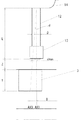
図1は実施形態の情報処理装置100の概略構成を模式的に示す説明図である。図2は光導波路基板1の分解した状態を示す説明である。図3(A)は光導波路基板2が備える光素子11を備えた光モジュール10の一部を示す正面図であり、図3(B)はその底面図である。図4(A)は光導波路基板1が備える基板本体の正面図、図4(B)は基板本体の一部を示す平面図、図4(C)は図(B)におけるA−A線断面図、図4(D)は図4(B)におけるB−B線断面図である。
式1
なお、光軸調整が行われ、光導波路3の下面における中心軸AX0と中心軸AX1との距離D=0.02mmが補正されると、嵌合部14から露出した光ファイバ12が角度θだけ傾く。上述の例において、この傾きθは、おおよそθ=0.2°程度となり、非常に微小である。このため、角度θが生じ、斜め入射となることに起因する損失は無視することができる。
式2

式3
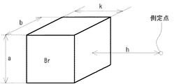
光ファイバ12の直径:
φ=0.125mm
第2の磁気部22の寸法:
a×b=0.55mm (磁束密度Bの算出に利用)
第1の磁気部13の寸法:
a’=b’=0.1mm (面積Sの算出に利用)
これにより、S=a’×b’=1×10⁻⁸m2
第2の磁気部22の厚み
k=0.65mm
ずれ量D=0.02mmのときの第1の磁気部13と第2の磁気部22との距離
h=0.46mm
残留磁束密度Br
Br=1200mT
2 基板本体
3 光導波路
4 ミラー部
5 位置決め穴
10、60 光モジュール
11 光素子
12 光ファイバ
12a 発光部
12b 射出部
12c 外周部
13 第1の磁気部
13a 内周面(S極)
13b 外周面(N極)
20 ケーブル保持部
21 ケーブル収容穴(円筒形状)
21a 内周壁
22 第2の磁気部
22a 内周面
22b 外周面
61 フレキシブルケーブル
100 情報処理装置
Claims (2)
- 並列配置された複数の光素子に対応させて複数の光導波路が形成された基板本体と、
先端部に前記光導波路と対向配置される入射部又は出射部を備える信号ケーブルであって、その外周部に第1の磁気部が設けられた信号ケーブルが収容される円筒形状のケーブル収容穴が複数の前記光導波路に対応させて設けられたケーブル保持部と、
前記ケーブル収容穴の内周壁に環状に設けられ、前記第1の磁気部との間で斥力を発生する第2の磁気部と、
を備え、
前記第1の磁気部は、前記信号ケーブルの前記外周部に環状に設けられ、
前記第2の磁気部は、その内周面が前記第1の磁気部の外周面と対向するように設けられた光導波路基板。 - 並列配置された複数の光素子と、
並列配置された複数の前記光素子に対応させて複数の光導波路が形成された基板本体と、
前記光素子から延設され、先端部に前記光導波路と対向配置される入射部又は出射部を備える信号ケーブルと、
前記信号ケーブルの外周部に設けられた第1の磁気部と、
前記信号ケーブルが収容される円筒形状のケーブル収容穴が複数の前記光導波路に対応させて設けられたケーブル保持部と、
前記ケーブル収容穴の内周壁に環状に設けられ、前記第1の磁気部との間で斥力を発生する第2の磁気部と、
を備え、
前記第1の磁気部は、前記信号ケーブルの前記外周部に環状に設けられ、
前記第2の磁気部は、その内周面が前記第1の磁気部の外周面と対向している、
情報処理装置。
Priority Applications (2)
| Application Number | Priority Date | Filing Date | Title |
|---|---|---|---|
| JP2013181621A JP6201537B2 (ja) | 2013-09-02 | 2013-09-02 | 光導波路基板及び情報処理装置 |
| US14/472,459 US9374163B2 (en) | 2013-09-02 | 2014-08-29 | Optical waveguide substrate and information processing device |
Applications Claiming Priority (1)
| Application Number | Priority Date | Filing Date | Title |
|---|---|---|---|
| JP2013181621A JP6201537B2 (ja) | 2013-09-02 | 2013-09-02 | 光導波路基板及び情報処理装置 |
Publications (2)
| Publication Number | Publication Date |
|---|---|
| JP2015049404A JP2015049404A (ja) | 2015-03-16 |
| JP6201537B2 true JP6201537B2 (ja) | 2017-09-27 |
Family
ID=52583388
Family Applications (1)
| Application Number | Title | Priority Date | Filing Date |
|---|---|---|---|
| JP2013181621A Expired - Fee Related JP6201537B2 (ja) | 2013-09-02 | 2013-09-02 | 光導波路基板及び情報処理装置 |
Country Status (2)
| Country | Link |
|---|---|
| US (1) | US9374163B2 (ja) |
| JP (1) | JP6201537B2 (ja) |
Families Citing this family (3)
| Publication number | Priority date | Publication date | Assignee | Title |
|---|---|---|---|---|
| JP6597193B2 (ja) * | 2015-11-02 | 2019-10-30 | 住友電気工業株式会社 | 光通信装置を作製する方法、光接続部品、光通信装置 |
| JP7541504B2 (ja) * | 2018-07-19 | 2024-08-28 | アルコン, インコーポレイテッド | 結合プラットフォームの自動調心素子用のラジアル反発型磁気軸受 |
| US11789215B2 (en) | 2019-06-25 | 2023-10-17 | Nippon Telegraph And Telephone Corporation | Optical connector and optical connecting structure |
Family Cites Families (34)
| Publication number | Priority date | Publication date | Assignee | Title |
|---|---|---|---|---|
| US3611815A (en) * | 1969-12-24 | 1971-10-12 | Us Navy | Frictionless gyroscope |
| US3810258A (en) * | 1972-07-11 | 1974-05-07 | W Mathauser | Quick connect electrical coupler |
| US4004298A (en) * | 1975-03-31 | 1977-01-25 | Sinai Hospital Of Detroit | Magnetically aligned releasable connector |
| JPS5553306A (en) * | 1978-10-17 | 1980-04-18 | Nippon Telegr & Teleph Corp <Ntt> | Connecting method of optical fiber |
| JPS56130903U (ja) * | 1980-03-04 | 1981-10-05 | ||
| JPS6140917U (ja) * | 1984-08-21 | 1986-03-15 | ティーディーケイ株式会社 | 連結部材の止め機構 |
| US4844582A (en) * | 1987-12-09 | 1989-07-04 | Giannini Gabriel M | Hybrid electro-optical connectors |
| JPH01173712A (ja) | 1987-12-28 | 1989-07-10 | Mitsubishi Electric Corp | 半導体装置の製造方法 |
| JPH01302210A (ja) * | 1988-05-30 | 1989-12-06 | Mitsubishi Cable Ind Ltd | 光分岐結合器 |
| JP3007181B2 (ja) | 1991-04-05 | 2000-02-07 | 株式会社ショーワ | 円筒状中空体内周溝成形工具、成形装置および成形方法 |
| US5261015A (en) * | 1991-11-21 | 1993-11-09 | Ametek, Inc. | Magnetically-actuatable opto-mechanical on/off switch and systems for use therewith |
| JPH0675141A (ja) * | 1992-08-27 | 1994-03-18 | Mitsubishi Gas Chem Co Inc | 光レセプタクル付き光導波路型部品 |
| US5359686A (en) * | 1993-03-29 | 1994-10-25 | Motorola, Inc. | Interface for coupling optical fibers to electronic circuitry |
| US5954520A (en) * | 1996-12-19 | 1999-09-21 | Schmidt; William P. | Magnetic coupler |
| US6102582A (en) * | 1998-09-21 | 2000-08-15 | Lucent Technologies Inc. | Article comprising controllable optical connectors |
| JP4090002B2 (ja) * | 2001-02-21 | 2008-05-28 | ケル株式会社 | カードコネクタ |
| JP2002311297A (ja) * | 2001-04-13 | 2002-10-23 | Nec Corp | 光ファイバコネクタおよび光スイッチ |
| US6896421B2 (en) * | 2003-02-26 | 2005-05-24 | Lockheed Martin Corporation | Method and apparatus for assembly of an optoelectronic device with an optical connector |
| JP2005267943A (ja) * | 2004-03-17 | 2005-09-29 | Jamco Corp | オーディオプラグ |
| US7311526B2 (en) * | 2005-09-26 | 2007-12-25 | Apple Inc. | Magnetic connector for electronic device |
| JP2007272047A (ja) | 2006-03-31 | 2007-10-18 | Japan Aviation Electronics Industry Ltd | 光部品 |
| JPWO2008023508A1 (ja) | 2006-08-22 | 2010-01-07 | 日本電気株式会社 | 光コネクタ及び光結合構造 |
| US7817005B2 (en) * | 2008-04-04 | 2010-10-19 | Cedar Ridge Research, Llc. | Correlated magnetic container and method for using the correlated magnetic container |
| US7755462B2 (en) * | 2008-04-04 | 2010-07-13 | Cedar Ridge Research Llc | Ring magnet structure having a coded magnet pattern |
| US7817006B2 (en) * | 2008-05-20 | 2010-10-19 | Cedar Ridge Research, Llc. | Apparatuses and methods relating to precision attachments between first and second components |
| US7841776B2 (en) * | 2008-09-30 | 2010-11-30 | Apple Inc. | Magnetic connector with optical signal path |
| US8388353B2 (en) * | 2009-03-11 | 2013-03-05 | Cercacor Laboratories, Inc. | Magnetic connector |
| US8315492B2 (en) * | 2009-04-24 | 2012-11-20 | Avago Technologies Fiber Ip (Singapore) Pte. Ltd | Fiber connector module including integrated optical lens turn block and method for coupling optical signals between a transceiver module and an optical fiber |
| US8295671B2 (en) * | 2009-10-15 | 2012-10-23 | Corning Incorporated | Coated optical fibers and related apparatuses, links, and methods for providing optical attenuation |
| US9590352B2 (en) * | 2010-07-21 | 2017-03-07 | Apple Inc. | Magnetically-implemented security devices |
| TWI493896B (zh) * | 2010-12-30 | 2015-07-21 | Hon Hai Prec Ind Co Ltd | 光纖通訊裝置 |
| TWI497142B (zh) * | 2011-01-26 | 2015-08-21 | Hon Hai Prec Ind Co Ltd | 光纖連接器 |
| JP6435194B2 (ja) * | 2011-12-14 | 2018-12-05 | ケッサ・インコーポレーテッド | 触覚フィードバックを提供するコネクタ |
| US20140120746A1 (en) * | 2012-10-24 | 2014-05-01 | Rostislav Persion | Electrical and fiber optic connector with magnetic electrical contacts |
-
2013
- 2013-09-02 JP JP2013181621A patent/JP6201537B2/ja not_active Expired - Fee Related
-
2014
- 2014-08-29 US US14/472,459 patent/US9374163B2/en not_active Expired - Fee Related
Also Published As
| Publication number | Publication date |
|---|---|
| US9374163B2 (en) | 2016-06-21 |
| US20150063746A1 (en) | 2015-03-05 |
| JP2015049404A (ja) | 2015-03-16 |
Similar Documents
| Publication | Publication Date | Title |
|---|---|---|
| JP6264832B2 (ja) | 光コネクタ、これを用いた電子機器、及び光コネクタの実装方法 | |
| JP6379642B2 (ja) | 光学装置の製造方法、光学装置及び光学コネクタユニット | |
| US9435925B2 (en) | Optical fiber cable connecting structure | |
| JP2013025092A5 (ja) | ||
| US20160091677A1 (en) | Optical signal processor and optical assembly | |
| JP6597193B2 (ja) | 光通信装置を作製する方法、光接続部品、光通信装置 | |
| JP6201537B2 (ja) | 光導波路基板及び情報処理装置 | |
| JP6379968B2 (ja) | 光ケーブル端末 | |
| JP2006106680A (ja) | 光素子モジュール及び光送受信機 | |
| CN104076453A (zh) | 光模块、光通信设备、以及光传送装置 | |
| JP2019045794A (ja) | 屈曲部を有する光ファイバの製造装置および製造方法 | |
| EP2860561B1 (en) | Light source device | |
| JP2014071414A (ja) | 光モジュール及び光モジュールの製造方法 | |
| JP6561491B2 (ja) | テープファイバの接続構造、及び、製造方法 | |
| WO2012008530A1 (ja) | 光通信モジュール | |
| CN103038683A (zh) | 光学准直器和使用了光学准直器的光学连接器 | |
| US20180372970A1 (en) | Optical connecting device, light processing apparatus, method for fabricting optical connecting device | |
| JP5879810B2 (ja) | 光モジュール及び光モジュール付きケーブル | |
| JP2015175910A (ja) | 光モジュール | |
| JP5698277B2 (ja) | 光結合方法及びコネクタ付きケーブルの製造方法 | |
| JP6421557B2 (ja) | 光モジュール及び光ケーブル | |
| JP5417546B1 (ja) | コネクタ付きケーブル及び光電変換用基板 | |
| JP2016090858A (ja) | 光アセンブリ | |
| US20120020623A1 (en) | Fiber connector assembly | |
| JP6551077B2 (ja) | 光モジュール |
Legal Events
| Date | Code | Title | Description |
|---|---|---|---|
| A621 | Written request for application examination |
Free format text: JAPANESE INTERMEDIATE CODE: A621 Effective date: 20160510 |
|
| A977 | Report on retrieval |
Free format text: JAPANESE INTERMEDIATE CODE: A971007 Effective date: 20170125 |
|
| A131 | Notification of reasons for refusal |
Free format text: JAPANESE INTERMEDIATE CODE: A131 Effective date: 20170131 |
|
| A521 | Request for written amendment filed |
Free format text: JAPANESE INTERMEDIATE CODE: A523 Effective date: 20170330 |
|
| TRDD | Decision of grant or rejection written | ||
| A01 | Written decision to grant a patent or to grant a registration (utility model) |
Free format text: JAPANESE INTERMEDIATE CODE: A01 Effective date: 20170801 |
|
| A61 | First payment of annual fees (during grant procedure) |
Free format text: JAPANESE INTERMEDIATE CODE: A61 Effective date: 20170814 |
|
| R150 | Certificate of patent or registration of utility model |
Ref document number: 6201537 Country of ref document: JP Free format text: JAPANESE INTERMEDIATE CODE: R150 |
|
| LAPS | Cancellation because of no payment of annual fees |