JP6201537B2 - Optical waveguide substrate and information processing apparatus - Google Patents
Optical waveguide substrate and information processing apparatus Download PDFInfo
- Publication number
- JP6201537B2 JP6201537B2 JP2013181621A JP2013181621A JP6201537B2 JP 6201537 B2 JP6201537 B2 JP 6201537B2 JP 2013181621 A JP2013181621 A JP 2013181621A JP 2013181621 A JP2013181621 A JP 2013181621A JP 6201537 B2 JP6201537 B2 JP 6201537B2
- Authority
- JP
- Japan
- Prior art keywords
- optical
- magnetic part
- cable
- magnetic
- optical waveguide
- Prior art date
- Legal status (The legal status is an assumption and is not a legal conclusion. Google has not performed a legal analysis and makes no representation as to the accuracy of the status listed.)
- Expired - Fee Related
Links
Images


Classifications
-
- H—ELECTRICITY
- H04—ELECTRIC COMMUNICATION TECHNIQUE
- H04B—TRANSMISSION
- H04B10/00—Transmission systems employing electromagnetic waves other than radio-waves, e.g. infrared, visible or ultraviolet light, or employing corpuscular radiation, e.g. quantum communication
- H04B10/25—Arrangements specific to fibre transmission
- H04B10/2589—Bidirectional transmission
- H04B10/25891—Transmission components
-
- G—PHYSICS
- G02—OPTICS
- G02B—OPTICAL ELEMENTS, SYSTEMS OR APPARATUS
- G02B6/00—Light guides; Structural details of arrangements comprising light guides and other optical elements, e.g. couplings
- G02B6/24—Coupling light guides
- G02B6/42—Coupling light guides with opto-electronic elements
- G02B6/4201—Packages, e.g. shape, construction, internal or external details
- G02B6/4204—Packages, e.g. shape, construction, internal or external details the coupling comprising intermediate optical elements, e.g. lenses, holograms
- G02B6/421—Packages, e.g. shape, construction, internal or external details the coupling comprising intermediate optical elements, e.g. lenses, holograms the intermediate optical component consisting of a short length of fibre, e.g. fibre stub
-
- G—PHYSICS
- G02—OPTICS
- G02B—OPTICAL ELEMENTS, SYSTEMS OR APPARATUS
- G02B6/00—Light guides; Structural details of arrangements comprising light guides and other optical elements, e.g. couplings
- G02B6/24—Coupling light guides
- G02B6/42—Coupling light guides with opto-electronic elements
- G02B6/4201—Packages, e.g. shape, construction, internal or external details
- G02B6/4204—Packages, e.g. shape, construction, internal or external details the coupling comprising intermediate optical elements, e.g. lenses, holograms
- G02B6/4214—Packages, e.g. shape, construction, internal or external details the coupling comprising intermediate optical elements, e.g. lenses, holograms the intermediate optical element having redirecting reflective means, e.g. mirrors, prisms for deflecting the radiation from horizontal to down- or upward direction toward a device
-
- G—PHYSICS
- G02—OPTICS
- G02B—OPTICAL ELEMENTS, SYSTEMS OR APPARATUS
- G02B6/00—Light guides; Structural details of arrangements comprising light guides and other optical elements, e.g. couplings
- G02B6/24—Coupling light guides
- G02B6/42—Coupling light guides with opto-electronic elements
- G02B6/43—Arrangements comprising a plurality of opto-electronic elements and associated optical interconnections
Landscapes
- Physics & Mathematics (AREA)
- General Physics & Mathematics (AREA)
- Optics & Photonics (AREA)
- Engineering & Computer Science (AREA)
- Electromagnetism (AREA)
- Computer Networks & Wireless Communication (AREA)
- Signal Processing (AREA)
- Optical Couplings Of Light Guides (AREA)
- Microelectronics & Electronic Packaging (AREA)
Description
本発明は、光導波路基板及び情報処理装置に関する。 The present invention relates to an optical waveguide substrate and an information processing apparatus.
従来、情報処理装置等の機器における高速データ伝送を行うものとして、光素子と光導波路を用いたインターコネクト技術が知られている。インターコネクト技術においては、光素子と光導波路との間の光結合を行う際の光軸調整がデータ伝送の質に影響を及ぼす。このため、光結合損失を低減するものとして、例えば、光データリンク用コネクタ(特許文献1参照)、光ファイバと光導波路の接続構造(特許文献2参照)が知られている。これら以外にも、関連があると考えられる文献として、例えば、特許文献3や特許文献4がある。
2. Description of the Related Art Conventionally, an interconnect technology using an optical element and an optical waveguide is known as a device that performs high-speed data transmission in an apparatus such as an information processing apparatus. In the interconnect technology, the optical axis adjustment when optical coupling between the optical element and the optical waveguide affects the quality of data transmission. For this reason, for reducing optical coupling loss, for example, an optical data link connector (see Patent Document 1) and a connection structure between an optical fiber and an optical waveguide (see Patent Document 2) are known. Besides these, there are, for example,
上記特許文献の多くは、光導波路が形成された基板と光ファイバの保持具との位置決めを容易に行うことができる構造とすることにより、光結合損失の低減を図っている。しかしながら、複数の発光部又は受光部を備えた光素子をそれぞれ光導波路上に搭載する場合に、すべての発光部又は受光部に対する光軸調整を行うのは多大な労力を伴う。 Many of the above-mentioned patent documents attempt to reduce optical coupling loss by adopting a structure in which the substrate on which the optical waveguide is formed and the optical fiber holder can be easily positioned. However, when an optical element having a plurality of light emitting units or light receiving units is mounted on the optical waveguide, it is very laborious to adjust the optical axes for all the light emitting units or light receiving units.
そこで、本明細書開示の光導波路基板及び情報処理装置は、データ伝送を行う光導波路と光素子との間の光軸調整を適切に行うことを課題とする。なお、前記課題に限らず、後述する発明を実施するための形態に示す各構成により導かれる作用効果であって、従来の技術によっては得られない作用効果を奏することも本発明の他の課題の1つとして位置付けることができる。 Therefore, an object of the optical waveguide substrate and the information processing apparatus disclosed in this specification is to appropriately adjust the optical axis between an optical waveguide that performs data transmission and an optical element. In addition, the present invention is not limited to the above-described problems, and is an operational effect derived from each configuration shown in the embodiment for carrying out the invention to be described later. Can be positioned as one of
本明細書開示の光導波路基板は、並列配置された複数の光素子に対応させて複数の光導波路が形成された基板本体と、先端部に前記光導波路と対向配置される入射部又は出射部を備える信号ケーブルであって、その外周部に第1の磁気部が設けられた信号ケーブルが収容される円筒形状のケーブル収容穴が複数の前記光導波路に対応させて設けられたケーブル保持部と、前記ケーブル収容穴の内周壁に環状に設けられ、前記第1の磁気部との間で斥力を発生する第2の磁気部と、を備え、前記第1の磁気部は、前記信号ケーブルの前記外周部に環状に設けられ、前記第2の磁気部は、その内周面が前記第1の磁気部の外周面と対向するように設けられている。 An optical waveguide substrate disclosed in the present specification includes a substrate body in which a plurality of optical waveguides are formed corresponding to a plurality of optical elements arranged in parallel, and an incident portion or an emission portion that is disposed to face the optical waveguide at a tip portion. A cable holding portion provided with a cylindrical cable housing hole corresponding to the plurality of optical waveguides, in which a signal cable having a first magnetic portion provided on the outer periphery thereof is accommodated. A second magnetic part provided in an annular shape on the inner peripheral wall of the cable housing hole and generating a repulsive force with the first magnetic part, wherein the first magnetic part is provided on the signal cable. The second magnetic part is provided in an annular shape on the outer peripheral part, and the inner peripheral face thereof is provided so as to face the outer peripheral face of the first magnetic part .
また、本明細書開示の情報処理装置は、並列配置された複数の光素子と、並列配置された複数の前記光素子に対応させて複数の光導波路が形成された基板本体と、前記光素子から延設され、先端部に前記光導波路と対向配置される入射部又は出射部を備える信号ケーブルと、前記信号ケーブルの外周部に設けられた第1の磁気部と、前記信号ケーブルが収容される円筒形状のケーブル収容穴が複数の前記光導波路に対応させて設けられたケーブル保持部と、前記ケーブル収容穴の内周壁に環状に設けられ、前記第1の磁気部との間で斥力を発生する第2の磁気部と、を備え、前記第1の磁気部は、前記信号ケーブルの前記外周部に環状に設けられ、前記第2の磁気部は、その内周面が前記第1の磁気部の外周面と対向している。 Further, the information processing apparatus disclosed in the present specification includes a plurality of optical elements arranged in parallel, a substrate body in which a plurality of optical waveguides are formed corresponding to the plurality of optical elements arranged in parallel, and the optical element extending from a signal cable comprising the optical waveguide and incident portion or emitting portion is disposed opposite the tip, the first magnetic portion formed on the outer peripheral portion of the signal cable, the signal cable is accommodated a cable holding portion for the cable receiving bore of the cylindrical shape is provided corresponding to a plurality of the optical waveguide that is provided on the annular inner peripheral wall of the cable receiving hole, the repulsive force between the first magnetic portion A second magnetic part that is generated , wherein the first magnetic part is annularly provided on the outer peripheral part of the signal cable, and the inner peripheral surface of the second magnetic part is the first magnetic part. It faces the outer peripheral surface of the magnetic part .
第1の磁気部と第2の磁気部との間に生じる斥力によって自律的に信号ケーブルの光軸調整が行われる。 The optical axis of the signal cable is autonomously adjusted by the repulsive force generated between the first magnetic part and the second magnetic part.
本明細書開示の光導波路基板及び情報処理装置によれば、データ伝送を行う光導波路と光素子との間の光軸調整を適切に行うことができる。 According to the optical waveguide substrate and the information processing apparatus disclosed in this specification, it is possible to appropriately adjust the optical axis between the optical waveguide that performs data transmission and the optical element.
以下、本発明の実施形態について、添付図面を参照しつつ説明する。ただし、図面中、各部の寸法、比率等は、実際のものと完全に一致するようには図示されていない場合がある。また、図面によっては、説明の都合上、実際には存在する構成要素が省略されていたり、寸法が実際よりも誇張されて描かれていたりする場合がある。なお、以下の説明において、前後方向、左右方向、上下方向を図2に示す方向とする。 Hereinafter, embodiments of the present invention will be described with reference to the accompanying drawings. However, in the drawings, the dimensions, ratios, and the like of each part may not be shown so as to completely match the actual ones. Further, depending on the drawings, components that are actually present may be omitted for convenience of explanation, or dimensions may be exaggerated from the actual drawing. In the following description, the front-rear direction, the left-right direction, and the up-down direction are directions shown in FIG.
(実施形態)
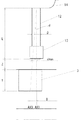
図1は実施形態の情報処理装置100の概略構成を模式的に示す説明図である。図2は光導波路基板1の分解した状態を示す説明である。図3(A)は光導波路基板2が備える光素子11を備えた光モジュール10の一部を示す正面図であり、図3(B)はその底面図である。図4(A)は光導波路基板1が備える基板本体の正面図、図4(B)は基板本体の一部を示す平面図、図4(C)は図(B)におけるA−A線断面図、図4(D)は図4(B)におけるB−B線断面図である。
(Embodiment)
FIG. 1 is an explanatory diagram schematically illustrating a schematic configuration of an
図1を参照すると、情報処理装置100は、光インターコネクティングによりデータ伝送を行う光導波路基板1を備える。光導波路基板1は、前後方向に延びる複数の光導波路3が形成された基板本体2を備える。光導波路3のそれぞれの端部には、光モジュール10が設置されている。光モジュール10には、それぞれIC(Integrated Circuit)15が接続されている。このような情報処理装置100は、光導波路基板1を備える装置の一例であり、光導波路基板1は、データ伝送処理を行う他の装置に搭載することもできる。
Referring to FIG. 1, an
図2を参照すると、光導波路基板2は、左右方向に並列して配置された光導波路3の端部にそれぞれミラー部4を備える。ミラー部4は、光を屈曲させ、光路を変換する。光導波路基板2は、光導波路3の端部を覆うように設けられたケーブル保持部20を備える。ケーブル保持部20には、ミラー部4の位置に対応させて設けられた複数のケーブル収容穴21が設けられている。ケーブル収容穴21は、円筒形状をなしている。ケーブル保持部20は、ブロック状の部材であり、このケーブル保持部20の上側に光モジュール10が搭載される。
Referring to FIG. 2, the
図3を参照すると、光モジュール10は、内部に光素子11を備える。光素子11は、発光素子であり、発光部12aを備える。この発光部12aは、光素子11が受光素子である場合には、受光部となる。光モジュール10は、光素子11から延設された光ファイバ12を備える。光ファイバ12は、データ伝送を行う信号ケーブルに相当するものであり、光モジュール10の本体部10aから外部へ延出した状態とされている。光ファイバ12は、可撓性を有する。信号ケーブルとしては、可撓性を有する他の信号線を用いてもよい。光ファイバ12は、光素子11側と異なる端部に光導波路3と対向配置される射出部12bを備える。この射出部12bは、光素子11が受光素子である場合には、入射部となる。光ファイバ12の外周部12bには、第1の磁気部13が設けられている。第1の磁気部13は、光ファイバ12の先端部に設けられている。第1の磁気部13は、光ファイバ12の外周部に環状に設けられており、内周面13a側がS極とされ、外周面13b側がN極とされている。なお、後述する第2の磁気部22との関係で、S極とN極とを入れ換えて設定することもできる。第1の磁気部13は、磁性体又は磁石によって形成することができる。第1の磁気部13は、例えば、予めパイプ状に成形された部材を装着するようにしてもよい。本実施形態の第1の磁気部13は、ネオジム系の磁性体を液浸や、塗布により光ファイバ12の先端部に付着させ、その後、加熱等により硬化させ、外部磁界によって磁化させて設けられている。
Referring to FIG. 3, the
図4(A)〜(D)を参照すると、ケーブル保持部20は、ミラー部4の位置に対応させて設けられたケーブル収容穴21のそれぞれの内周壁21aに第2の磁気部22を備えている。第2の磁気部22は、磁性体又は磁石によって形成することができる。第2の磁気部22は、第1の磁気部13との間で斥力を発生させる。本実施形態の第1の磁気部13は、上述の如く、内周面13a側をS極とし、外周面13b側をN極としている。そこで、図5を参照すると、第2の磁気部22は、第1の磁気部13の外周面13bと対向する内周面22a側をN極とし、外周面22bをS極としている。これにより、第1の磁気部13と第2の磁気部22との間に斥力が発生する。なお、第1の磁気部13におけるS極とN極とが入れ換えて設定されている場合には、これに合わせて第2の磁気部22のS極とN極も入れ換えて設定される。要は、第1の磁気部13と第2の磁気部22とが相互に対向する面に同極が配置された状態となっていればよい。
Referring to FIGS. 4A to 4D, the
ケーブル保持部20は、基板本体2と接合される際、ケーブル収容穴21の中心軸AX0とミラー部4の中心とがそれぞれ一致するように位置決めされる。ケーブル保持部20は、下面に位置決めピン23を備えている。この位置決めピン23が、基板本体2に設けられた位置決め穴5に挿し込まれることによって、ケーブル保持部20の基板本体2への位置決めがされる。ケーブル保持部20と基板本体2とは、位置決めピン23を用いて接合状態とすることができるが、本実施形態では、さらにUV硬化樹脂を用いて接着されている。両者の接着には、従来公知の種々の接着方法や接着剤を用いることができる。
When the
図6(A)、(B)を参照すると、光ファイバ12がそれぞれケーブル収容穴21内に収容されるように、光モジュール10がケーブル保持部20上に搭載される。光モジュール10には、嵌合部14が設けられており、この嵌合部14がケーブル収容穴21の上端部に形成されたテーパ部に嵌め込まれる。このとき、図7に示すように、光ファイバ12の中心軸AX1がケーブル収容穴21の中心軸AX0と一致することが望ましい。
6A and 6B, the
ところが、図8(A)で示すように、光ファイバ12の中心軸AX1がケーブル収容穴21の中心軸AX0と一致せず、光軸がずれた状態となることがある。このような状態に対し、本実施形態の光導波路基板1では、図8(B)に示すように第1の磁気部13と第2の磁気部22との磁力、換言すれば両者間に生じる斥力によって自律的に光ファイバ12の光軸調整が行われる。すなわち、磁力によって光ファイバ12の先端部である射出部12bが、ケーブル収容穴21の中心軸AX0と一致するように誘導される。以下、このような光軸調整について、近似モデルを用いて説明する。
However, as shown in FIG. 8A, the central axis AX1 of the
図9はケーブル収容穴21の中心軸AX0と光ファイバの中心軸AX1とが距離Dだけずれた状態を示す説明である。光ファイバ12を撓ませて光軸調整するために必要となる荷重Pを簡易的に算出する。具体的に、射出部12bの位置をケーブル収容穴21の中心側に向かって反り量dmaxだけ移動させることによって光軸調整がされる場合に必要となる荷重Pを算出する。
FIG. 9 is an illustration showing a state in which the center axis AX0 of the
光ファイバ12の直径φをφ=0.125mm、光ファイバ12の自由長、すなわち、光ファイバ12が嵌合部14から露出した部分の長さLをL=5mm、射出部12bから光導波路3の上面までの距離ZをZ=0.5mmであると仮定する。さらに、光導波路3のコアサイズ(光導波路の一辺の長さ)YをY=0.05mm、ヤング率EをE=3000N/mm2、光導波路3の下面における中心軸AX0と中心軸AX1との距離DをD=0.02mmであると仮定する。以上のような条件において、必要な荷重Pは、以下の式1
式1
![]()
なお、光軸調整が行われ、光導波路3の下面における中心軸AX0と中心軸AX1との距離D=0.02mmが補正されると、嵌合部14から露出した光ファイバ12が角度θだけ傾く。上述の例において、この傾きθは、おおよそθ=0.2°程度となり、非常に微小である。このため、角度θが生じ、斜め入射となることに起因する損失は無視することができる。
The diameter φ of the
![]()
When the optical axis is adjusted and the distance D = 0.02 mm between the central axis AX0 and the central axis AX1 on the lower surface of the
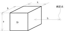
つぎに、図10、図11を参照して、第1の磁気部13と第2の磁気部22とによって発生する磁力について検討する。まず、図10を参照して、残留磁束密度がBrであり、寸法がa×b×kの磁性体が距離hだけ離れた測定点に及ぼす磁束密度Bについて説明する。測定点での磁束密度Bは、以下の式2で表される。
式2

ここで、測定点付近での磁束が一様であると仮定し、さらに、斥力は吸引力の50%〜70%となることを考慮して、斥力は、吸引力の60%であるとして、以下の式3で表される。
式3
![]()
![]()
以上のような関係を本実施形態の光導波路基板1に当て嵌めて検証する。光導波路基板1の各部の寸法は、以下のように仮定する。
光ファイバ12の直径:
φ=0.125mm
第2の磁気部22の寸法:
a×b=0.55mm (磁束密度Bの算出に利用)
第1の磁気部13の寸法:
a’=b’=0.1mm (面積Sの算出に利用)
これにより、S=a’×b’=1×10⁻⁸m2
第2の磁気部22の厚み
k=0.65mm
ずれ量D=0.02mmのときの第1の磁気部13と第2の磁気部22との距離
h=0.46mm
残留磁束密度Br
Br=1200mT
The above relationship is applied to the
Diameter of optical fiber 12:
φ = 0.125mm
Dimensions of the second magnetic part 22:
a × b = 0.55mm (used to calculate magnetic flux density B)
Dimensions of the first magnetic part 13:
a ′ = b ′ = 0.1 mm (used to calculate area S)
Thereby, S = a ′ × b ′ = 1 × 10 −8 m 2
The thickness of the second magnetic part 22 k = 0.65 mm
Distance between first
Residual magnetic flux density Br
Br = 1200mT
以上の条件で斥力Fを算出すると、F≒1.52mgfとなる。この値を、上述の荷重Pと比較すると、ほぼ近い値となり、光ファイバ12を撓ませることによる光軸調整が可能であることが検証された。磁力は、第1の磁気部13及び第2の磁気部22との間の距離によって変化するため、第1の磁気部13は、周囲の磁力がバランスした位置に収束する。
When the repulsive force F is calculated under the above conditions, F≈1.52 mgf. When this value is compared with the above-described load P, the value is almost close, and it has been verified that the optical axis can be adjusted by bending the
以上のように、本実施形態の光導波路基板1は、磁力により自律的な光軸調整が行われる。このような自律的な光軸調整は、各光ファイバ12において行われるため、光軸調整の労力低減となる。また、光素子の実装にはんだ接合を用いた場合、その熱により部材に膨張、反りが生じ、光軸に影響を与えることがあるが、本実施形態の光導波路基板1であれば、光軸は自己調整される。
As described above, the
なお、上記実施形態では、信号ケーブルとして光ファイバ12を用いているが、図12に示すように、信号ケーブルとしてフレキシブルケーブル61を用いることもできる。すなわち、光モジュール60は、光素子11から延設されたフレキシブルケーブル61を備え、その先端部に第1の磁気部13が設けられている。なお、フレキシブルケーブルは、内部に電気信号を伝送する金属線を備えており、先端部に受光部(又は発光部)62を備える。このようなフレキシブルケーブル61に対しても第1の磁気部13と第2の磁気部22との間に生じる斥力が作用し、光軸の自己調整が行われる。
In the above embodiment, the
1 光導波路基板
2 基板本体
3 光導波路
4 ミラー部
5 位置決め穴
10、60 光モジュール
11 光素子
12 光ファイバ
12a 発光部
12b 射出部
12c 外周部
13 第1の磁気部
13a 内周面(S極)
13b 外周面(N極)
20 ケーブル保持部
21 ケーブル収容穴(円筒形状)
21a 内周壁
22 第2の磁気部
22a 内周面
22b 外周面
61 フレキシブルケーブル
100 情報処理装置
DESCRIPTION OF
13b Outer peripheral surface (N pole)
20
21a Inner
Claims (2)
先端部に前記光導波路と対向配置される入射部又は出射部を備える信号ケーブルであって、その外周部に第1の磁気部が設けられた信号ケーブルが収容される円筒形状のケーブル収容穴が複数の前記光導波路に対応させて設けられたケーブル保持部と、
前記ケーブル収容穴の内周壁に環状に設けられ、前記第1の磁気部との間で斥力を発生する第2の磁気部と、
を備え、
前記第1の磁気部は、前記信号ケーブルの前記外周部に環状に設けられ、
前記第2の磁気部は、その内周面が前記第1の磁気部の外周面と対向するように設けられた光導波路基板。 A substrate body having a plurality of optical waveguides formed corresponding to the plurality of optical elements arranged in parallel ;
A signal cable having an incident part or an emission part arranged opposite to the optical waveguide at the tip part, and a cylindrical cable accommodation hole for accommodating the signal cable provided with the first magnetic part on the outer peripheral part thereof A cable holding portion provided corresponding to the plurality of optical waveguides ;
A second magnetic part that is annularly provided on the inner peripheral wall of the cable housing hole and generates a repulsive force with the first magnetic part;
Equipped with a,
The first magnetic part is provided annularly on the outer peripheral part of the signal cable,
The second magnetic part is an optical waveguide substrate provided so that an inner peripheral surface thereof faces an outer peripheral surface of the first magnetic part .
並列配置された複数の前記光素子に対応させて複数の光導波路が形成された基板本体と、
前記光素子から延設され、先端部に前記光導波路と対向配置される入射部又は出射部を備える信号ケーブルと、
前記信号ケーブルの外周部に設けられた第1の磁気部と、
前記信号ケーブルが収容される円筒形状のケーブル収容穴が複数の前記光導波路に対応させて設けられたケーブル保持部と、
前記ケーブル収容穴の内周壁に環状に設けられ、前記第1の磁気部との間で斥力を発生する第2の磁気部と、
を備え、
前記第1の磁気部は、前記信号ケーブルの前記外周部に環状に設けられ、
前記第2の磁気部は、その内周面が前記第1の磁気部の外周面と対向している、
情報処理装置。 A plurality of optical elements arranged in parallel ;
A substrate body in which a plurality of optical waveguides are formed corresponding to the plurality of optical elements arranged in parallel ;
A signal cable that extends from the optical element and includes an incident part or an emission part that is disposed opposite to the optical waveguide at a tip part ;
A first magnetic part provided on the outer periphery of the signal cable;
A cable holding portion in which a cylindrical cable housing hole for accommodating the signal cable is provided corresponding to the plurality of the optical waveguides ;
A second magnetic part that is annularly provided on the inner peripheral wall of the cable housing hole and generates a repulsive force with the first magnetic part;
Equipped with a,
The first magnetic part is provided annularly on the outer peripheral part of the signal cable,
The second magnetic part has an inner peripheral surface facing the outer peripheral surface of the first magnetic part.
Information processing device.
Priority Applications (2)
| Application Number | Priority Date | Filing Date | Title |
|---|---|---|---|
| JP2013181621A JP6201537B2 (en) | 2013-09-02 | 2013-09-02 | Optical waveguide substrate and information processing apparatus |
| US14/472,459 US9374163B2 (en) | 2013-09-02 | 2014-08-29 | Optical waveguide substrate and information processing device |
Applications Claiming Priority (1)
| Application Number | Priority Date | Filing Date | Title |
|---|---|---|---|
| JP2013181621A JP6201537B2 (en) | 2013-09-02 | 2013-09-02 | Optical waveguide substrate and information processing apparatus |
Publications (2)
| Publication Number | Publication Date |
|---|---|
| JP2015049404A JP2015049404A (en) | 2015-03-16 |
| JP6201537B2 true JP6201537B2 (en) | 2017-09-27 |
Family
ID=52583388
Family Applications (1)
| Application Number | Title | Priority Date | Filing Date |
|---|---|---|---|
| JP2013181621A Expired - Fee Related JP6201537B2 (en) | 2013-09-02 | 2013-09-02 | Optical waveguide substrate and information processing apparatus |
Country Status (2)
| Country | Link |
|---|---|
| US (1) | US9374163B2 (en) |
| JP (1) | JP6201537B2 (en) |
Families Citing this family (3)
| Publication number | Priority date | Publication date | Assignee | Title |
|---|---|---|---|---|
| JP6597193B2 (en) * | 2015-11-02 | 2019-10-30 | 住友電気工業株式会社 | Method for manufacturing optical communication device, optical connection component, optical communication device |
| ES2935513T3 (en) * | 2018-07-19 | 2023-03-07 | Alcon Inc | Ophthalmic surgical system with radial repulsion magnetic bearing for self-alignment of optical elements |
| JP7279789B2 (en) * | 2019-06-25 | 2023-05-23 | 日本電信電話株式会社 | optical connection structure |
Family Cites Families (34)
| Publication number | Priority date | Publication date | Assignee | Title |
|---|---|---|---|---|
| US3611815A (en) * | 1969-12-24 | 1971-10-12 | Us Navy | Frictionless gyroscope |
| US3810258A (en) * | 1972-07-11 | 1974-05-07 | W Mathauser | Quick connect electrical coupler |
| US4004298A (en) * | 1975-03-31 | 1977-01-25 | Sinai Hospital Of Detroit | Magnetically aligned releasable connector |
| JPS5553306A (en) * | 1978-10-17 | 1980-04-18 | Nippon Telegr & Teleph Corp <Ntt> | Connecting method of optical fiber |
| JPS56130903U (en) * | 1980-03-04 | 1981-10-05 | ||
| JPS6140917U (en) * | 1984-08-21 | 1986-03-15 | ティーディーケイ株式会社 | Connecting member stopping mechanism |
| US4844582A (en) * | 1987-12-09 | 1989-07-04 | Giannini Gabriel M | Hybrid electro-optical connectors |
| JPH01173712A (en) | 1987-12-28 | 1989-07-10 | Mitsubishi Electric Corp | Manufacture of semiconductor device |
| JPH01302210A (en) * | 1988-05-30 | 1989-12-06 | Mitsubishi Cable Ind Ltd | Optical branching/coupling device |
| JP3007181B2 (en) | 1991-04-05 | 2000-02-07 | 株式会社ショーワ | Cylindrical hollow body circumferential groove forming tool, forming apparatus and forming method |
| US5261015A (en) * | 1991-11-21 | 1993-11-09 | Ametek, Inc. | Magnetically-actuatable opto-mechanical on/off switch and systems for use therewith |
| JPH0675141A (en) * | 1992-08-27 | 1994-03-18 | Mitsubishi Gas Chem Co Inc | Optical waveguide type component with optical receptacle |
| US5359686A (en) * | 1993-03-29 | 1994-10-25 | Motorola, Inc. | Interface for coupling optical fibers to electronic circuitry |
| US5954520A (en) * | 1996-12-19 | 1999-09-21 | Schmidt; William P. | Magnetic coupler |
| US6102582A (en) * | 1998-09-21 | 2000-08-15 | Lucent Technologies Inc. | Article comprising controllable optical connectors |
| JP4090002B2 (en) * | 2001-02-21 | 2008-05-28 | ケル株式会社 | Card connector |
| JP2002311297A (en) * | 2001-04-13 | 2002-10-23 | Nec Corp | Optical fiber connector and optical switch |
| US6896421B2 (en) * | 2003-02-26 | 2005-05-24 | Lockheed Martin Corporation | Method and apparatus for assembly of an optoelectronic device with an optical connector |
| JP2005267943A (en) * | 2004-03-17 | 2005-09-29 | Jamco Corp | Audio plug |
| US7311526B2 (en) * | 2005-09-26 | 2007-12-25 | Apple Inc. | Magnetic connector for electronic device |
| JP2007272047A (en) | 2006-03-31 | 2007-10-18 | Japan Aviation Electronics Industry Ltd | Optical component |
| WO2008023508A1 (en) | 2006-08-22 | 2008-02-28 | Nec Corporation | Optical connector and optical coupling structure |
| US7817005B2 (en) * | 2008-04-04 | 2010-10-19 | Cedar Ridge Research, Llc. | Correlated magnetic container and method for using the correlated magnetic container |
| US7755462B2 (en) * | 2008-04-04 | 2010-07-13 | Cedar Ridge Research Llc | Ring magnet structure having a coded magnet pattern |
| US7817006B2 (en) * | 2008-05-20 | 2010-10-19 | Cedar Ridge Research, Llc. | Apparatuses and methods relating to precision attachments between first and second components |
| US7841776B2 (en) * | 2008-09-30 | 2010-11-30 | Apple Inc. | Magnetic connector with optical signal path |
| US8388353B2 (en) * | 2009-03-11 | 2013-03-05 | Cercacor Laboratories, Inc. | Magnetic connector |
| US8315492B2 (en) * | 2009-04-24 | 2012-11-20 | Avago Technologies Fiber Ip (Singapore) Pte. Ltd | Fiber connector module including integrated optical lens turn block and method for coupling optical signals between a transceiver module and an optical fiber |
| US8295671B2 (en) * | 2009-10-15 | 2012-10-23 | Corning Incorporated | Coated optical fibers and related apparatuses, links, and methods for providing optical attenuation |
| US8963666B2 (en) * | 2010-07-21 | 2015-02-24 | Apple Inc. | Programmable magnetic connectors |
| TWI493896B (en) * | 2010-12-30 | 2015-07-21 | Hon Hai Prec Ind Co Ltd | Optical fiber communication apparatus |
| TWI497142B (en) * | 2011-01-26 | 2015-08-21 | Hon Hai Prec Ind Co Ltd | Optical fiber connector |
| WO2013090625A1 (en) * | 2011-12-14 | 2013-06-20 | Waveconnex, Inc. | Connectors providing haptic feedback |
| US20140120746A1 (en) * | 2012-10-24 | 2014-05-01 | Rostislav Persion | Electrical and fiber optic connector with magnetic electrical contacts |
-
2013
- 2013-09-02 JP JP2013181621A patent/JP6201537B2/en not_active Expired - Fee Related
-
2014
- 2014-08-29 US US14/472,459 patent/US9374163B2/en not_active Expired - Fee Related
Also Published As
| Publication number | Publication date |
|---|---|
| US20150063746A1 (en) | 2015-03-05 |
| US9374163B2 (en) | 2016-06-21 |
| JP2015049404A (en) | 2015-03-16 |
Similar Documents
| Publication | Publication Date | Title |
|---|---|---|
| JP6264832B2 (en) | Optical connector, electronic device using the same, and optical connector mounting method | |
| JP5302714B2 (en) | Optical connector | |
| US9435925B2 (en) | Optical fiber cable connecting structure | |
| US9372314B2 (en) | Optical signal processor and optical assembly | |
| JP6379642B2 (en) | Optical device manufacturing method, optical device, and optical connector unit | |
| JP2013025092A5 (en) | ||
| US20130272662A1 (en) | Connectored cable and method for manufacturing connectored cable | |
| JP2006106680A (en) | Optical device module, and optical transmitter and receiver | |
| JP6379968B2 (en) | Optical cable terminal | |
| JP6201537B2 (en) | Optical waveguide substrate and information processing apparatus | |
| JP2009047937A (en) | Optical transmission/optical reception module, method of manufacturing optical module and optical communication module | |
| JP2010016012A (en) | Photoelectric conversion device, photoelectric conversion module, and method of manufacturing photoelectric conversion device | |
| JP2019045794A (en) | Apparatus and method for manufacturing optical fiber having bent part | |
| JP6561491B2 (en) | Tape fiber connection structure and manufacturing method | |
| JP5250679B2 (en) | Cable with connector and method of manufacturing cable with connector | |
| JP2013041058A (en) | Optical module and cable with optical module | |
| JP5250680B2 (en) | Cable with connector and method of manufacturing cable with connector | |
| US20130129276A1 (en) | Optical engine assembly and optoelectronic package | |
| JP6421557B2 (en) | Optical module and optical cable | |
| JP5698277B2 (en) | Optical coupling method and manufacturing method of cable with connector | |
| JP5417546B1 (en) | Cable with connector and substrate for photoelectric conversion | |
| JP6551077B2 (en) | Optical module | |
| US9547126B2 (en) | Optical waveguide sheet, optical unit, and method for manufacturing the same | |
| JP2009223346A (en) | Optical transceiver | |
| TWI571664B (en) | Silicon bench |
Legal Events
| Date | Code | Title | Description |
|---|---|---|---|
| A621 | Written request for application examination |
Free format text: JAPANESE INTERMEDIATE CODE: A621 Effective date: 20160510 |
|
| A977 | Report on retrieval |
Free format text: JAPANESE INTERMEDIATE CODE: A971007 Effective date: 20170125 |
|
| A131 | Notification of reasons for refusal |
Free format text: JAPANESE INTERMEDIATE CODE: A131 Effective date: 20170131 |
|
| A521 | Request for written amendment filed |
Free format text: JAPANESE INTERMEDIATE CODE: A523 Effective date: 20170330 |
|
| TRDD | Decision of grant or rejection written | ||
| A01 | Written decision to grant a patent or to grant a registration (utility model) |
Free format text: JAPANESE INTERMEDIATE CODE: A01 Effective date: 20170801 |
|
| A61 | First payment of annual fees (during grant procedure) |
Free format text: JAPANESE INTERMEDIATE CODE: A61 Effective date: 20170814 |
|
| R150 | Certificate of patent or registration of utility model |
Ref document number: 6201537 Country of ref document: JP Free format text: JAPANESE INTERMEDIATE CODE: R150 |
|
| LAPS | Cancellation because of no payment of annual fees |