JP6182555B2 - Method for manufacturing SOI substrate - Google Patents
Method for manufacturing SOI substrate Download PDFInfo
- Publication number
- JP6182555B2 JP6182555B2 JP2015011075A JP2015011075A JP6182555B2 JP 6182555 B2 JP6182555 B2 JP 6182555B2 JP 2015011075 A JP2015011075 A JP 2015011075A JP 2015011075 A JP2015011075 A JP 2015011075A JP 6182555 B2 JP6182555 B2 JP 6182555B2
- Authority
- JP
- Japan
- Prior art keywords
- single crystal
- substrate
- layer
- silicon
- crystal silicon
- Prior art date
- Legal status (The legal status is an assumption and is not a legal conclusion. Google has not performed a legal analysis and makes no representation as to the accuracy of the status listed.)
- Expired - Lifetime
Links
- 239000000758 substrate Substances 0.000 title claims description 126
- 238000000034 method Methods 0.000 title claims description 48
- 238000004519 manufacturing process Methods 0.000 title claims description 18
- 229910021421 monocrystalline silicon Inorganic materials 0.000 claims description 79
- VYPSYNLAJGMNEJ-UHFFFAOYSA-N Silicium dioxide Chemical compound O=[Si]=O VYPSYNLAJGMNEJ-UHFFFAOYSA-N 0.000 claims description 41
- 229910052814 silicon oxide Inorganic materials 0.000 claims description 38
- 229910052739 hydrogen Inorganic materials 0.000 claims description 27
- 239000001257 hydrogen Substances 0.000 claims description 26
- 238000010438 heat treatment Methods 0.000 claims description 23
- UFHFLCQGNIYNRP-UHFFFAOYSA-N Hydrogen Chemical compound [H][H] UFHFLCQGNIYNRP-UHFFFAOYSA-N 0.000 claims description 22
- 239000010410 layer Substances 0.000 description 149
- 239000010408 film Substances 0.000 description 56
- 239000004065 semiconductor Substances 0.000 description 53
- XUIMIQQOPSSXEZ-UHFFFAOYSA-N Silicon Chemical compound [Si] XUIMIQQOPSSXEZ-UHFFFAOYSA-N 0.000 description 40
- 239000013078 crystal Substances 0.000 description 32
- 229910052710 silicon Inorganic materials 0.000 description 28
- 239000010703 silicon Substances 0.000 description 27
- 229910021426 porous silicon Inorganic materials 0.000 description 20
- 239000001301 oxygen Substances 0.000 description 16
- 229910052760 oxygen Inorganic materials 0.000 description 16
- QVGXLLKOCUKJST-UHFFFAOYSA-N atomic oxygen Chemical compound [O] QVGXLLKOCUKJST-UHFFFAOYSA-N 0.000 description 12
- 239000012535 impurity Substances 0.000 description 12
- 230000008569 process Effects 0.000 description 11
- 239000004973 liquid crystal related substance Substances 0.000 description 9
- 239000000463 material Substances 0.000 description 9
- 238000007254 oxidation reaction Methods 0.000 description 9
- 125000004429 atom Chemical group 0.000 description 8
- 238000005516 engineering process Methods 0.000 description 8
- 230000006870 function Effects 0.000 description 8
- 230000003647 oxidation Effects 0.000 description 8
- RTAQQCXQSZGOHL-UHFFFAOYSA-N Titanium Chemical compound [Ti] RTAQQCXQSZGOHL-UHFFFAOYSA-N 0.000 description 7
- 238000007743 anodising Methods 0.000 description 7
- -1 hydrogen ions Chemical class 0.000 description 7
- 229910021420 polycrystalline silicon Inorganic materials 0.000 description 7
- 230000001603 reducing effect Effects 0.000 description 7
- 239000010409 thin film Substances 0.000 description 7
- 239000010936 titanium Substances 0.000 description 7
- 229910052719 titanium Inorganic materials 0.000 description 7
- KRHYYFGTRYWZRS-UHFFFAOYSA-N Fluorane Chemical compound F KRHYYFGTRYWZRS-UHFFFAOYSA-N 0.000 description 6
- 238000000137 annealing Methods 0.000 description 6
- 230000015572 biosynthetic process Effects 0.000 description 6
- 239000011159 matrix material Substances 0.000 description 6
- 229910052581 Si3N4 Inorganic materials 0.000 description 5
- 229910017052 cobalt Inorganic materials 0.000 description 5
- 239000010941 cobalt Substances 0.000 description 5
- GUTLYIVDDKVIGB-UHFFFAOYSA-N cobalt atom Chemical compound [Co] GUTLYIVDDKVIGB-UHFFFAOYSA-N 0.000 description 5
- 238000012545 processing Methods 0.000 description 5
- HQVNEWCFYHHQES-UHFFFAOYSA-N silicon nitride Chemical compound N12[Si]34N5[Si]62N3[Si]51N64 HQVNEWCFYHHQES-UHFFFAOYSA-N 0.000 description 5
- QGZKDVFQNNGYKY-UHFFFAOYSA-N Ammonia Chemical compound N QGZKDVFQNNGYKY-UHFFFAOYSA-N 0.000 description 4
- LFQSCWFLJHTTHZ-UHFFFAOYSA-N Ethanol Chemical compound CCO LFQSCWFLJHTTHZ-UHFFFAOYSA-N 0.000 description 4
- 239000000919 ceramic Substances 0.000 description 4
- 238000006243 chemical reaction Methods 0.000 description 4
- 239000011259 mixed solution Substances 0.000 description 4
- 239000011347 resin Substances 0.000 description 4
- 229920005989 resin Polymers 0.000 description 4
- 230000000694 effects Effects 0.000 description 3
- 238000005530 etching Methods 0.000 description 3
- 238000000227 grinding Methods 0.000 description 3
- 239000011229 interlayer Substances 0.000 description 3
- 150000002500 ions Chemical class 0.000 description 3
- 229920005591 polysilicon Polymers 0.000 description 3
- 229910021332 silicide Inorganic materials 0.000 description 3
- FVBUAEGBCNSCDD-UHFFFAOYSA-N silicide(4-) Chemical compound [Si-4] FVBUAEGBCNSCDD-UHFFFAOYSA-N 0.000 description 3
- 235000012239 silicon dioxide Nutrition 0.000 description 3
- XKRFYHLGVUSROY-UHFFFAOYSA-N Argon Chemical compound [Ar] XKRFYHLGVUSROY-UHFFFAOYSA-N 0.000 description 2
- IJGRMHOSHXDMSA-UHFFFAOYSA-N Atomic nitrogen Chemical compound N#N IJGRMHOSHXDMSA-UHFFFAOYSA-N 0.000 description 2
- MHAJPDPJQMAIIY-UHFFFAOYSA-N Hydrogen peroxide Chemical compound OO MHAJPDPJQMAIIY-UHFFFAOYSA-N 0.000 description 2
- 239000004642 Polyimide Substances 0.000 description 2
- LEVVHYCKPQWKOP-UHFFFAOYSA-N [Si].[Ge] Chemical compound [Si].[Ge] LEVVHYCKPQWKOP-UHFFFAOYSA-N 0.000 description 2
- 229910021529 ammonia Inorganic materials 0.000 description 2
- 239000007864 aqueous solution Substances 0.000 description 2
- 229910052785 arsenic Inorganic materials 0.000 description 2
- RQNWIZPPADIBDY-UHFFFAOYSA-N arsenic atom Chemical compound [As] RQNWIZPPADIBDY-UHFFFAOYSA-N 0.000 description 2
- 230000008901 benefit Effects 0.000 description 2
- UMIVXZPTRXBADB-UHFFFAOYSA-N benzocyclobutene Chemical compound C1=CC=C2CCC2=C1 UMIVXZPTRXBADB-UHFFFAOYSA-N 0.000 description 2
- 230000008859 change Effects 0.000 description 2
- 238000009826 distribution Methods 0.000 description 2
- 238000005401 electroluminescence Methods 0.000 description 2
- 239000011521 glass Substances 0.000 description 2
- 238000005984 hydrogenation reaction Methods 0.000 description 2
- 239000012212 insulator Substances 0.000 description 2
- 238000000059 patterning Methods 0.000 description 2
- 238000005498 polishing Methods 0.000 description 2
- 238000007517 polishing process Methods 0.000 description 2
- 229920001721 polyimide Polymers 0.000 description 2
- 239000010453 quartz Substances 0.000 description 2
- 229910052715 tantalum Inorganic materials 0.000 description 2
- GUVRBAGPIYLISA-UHFFFAOYSA-N tantalum atom Chemical compound [Ta] GUVRBAGPIYLISA-UHFFFAOYSA-N 0.000 description 2
- ZOXJGFHDIHLPTG-UHFFFAOYSA-N Boron Chemical group [B] ZOXJGFHDIHLPTG-UHFFFAOYSA-N 0.000 description 1
- RYGMFSIKBFXOCR-UHFFFAOYSA-N Copper Chemical compound [Cu] RYGMFSIKBFXOCR-UHFFFAOYSA-N 0.000 description 1
- 229910000881 Cu alloy Inorganic materials 0.000 description 1
- 239000004952 Polyamide Substances 0.000 description 1
- 229910000577 Silicon-germanium Inorganic materials 0.000 description 1
- 229910002808 Si–O–Si Inorganic materials 0.000 description 1
- 229910001362 Ta alloys Inorganic materials 0.000 description 1
- NIXOWILDQLNWCW-UHFFFAOYSA-N acrylic acid group Chemical group C(C=C)(=O)O NIXOWILDQLNWCW-UHFFFAOYSA-N 0.000 description 1
- 239000000853 adhesive Substances 0.000 description 1
- 230000001070 adhesive effect Effects 0.000 description 1
- 229910052782 aluminium Inorganic materials 0.000 description 1
- XAGFODPZIPBFFR-UHFFFAOYSA-N aluminium Chemical compound [Al] XAGFODPZIPBFFR-UHFFFAOYSA-N 0.000 description 1
- 150000001408 amides Chemical class 0.000 description 1
- 229910021417 amorphous silicon Inorganic materials 0.000 description 1
- 229910052786 argon Inorganic materials 0.000 description 1
- 229910052799 carbon Inorganic materials 0.000 description 1
- 238000003776 cleavage reaction Methods 0.000 description 1
- 229910052681 coesite Inorganic materials 0.000 description 1
- 229910052802 copper Inorganic materials 0.000 description 1
- 239000010949 copper Substances 0.000 description 1
- 238000012937 correction Methods 0.000 description 1
- 229910052906 cristobalite Inorganic materials 0.000 description 1
- 229910021419 crystalline silicon Inorganic materials 0.000 description 1
- 238000010586 diagram Methods 0.000 description 1
- 238000009792 diffusion process Methods 0.000 description 1
- 230000005684 electric field Effects 0.000 description 1
- 239000012776 electronic material Substances 0.000 description 1
- 230000005669 field effect Effects 0.000 description 1
- 239000007789 gas Substances 0.000 description 1
- 239000002241 glass-ceramic Substances 0.000 description 1
- 125000004435 hydrogen atom Chemical group [H]* 0.000 description 1
- 125000002887 hydroxy group Chemical group [H]O* 0.000 description 1
- 238000002513 implantation Methods 0.000 description 1
- 238000005468 ion implantation Methods 0.000 description 1
- 238000005224 laser annealing Methods 0.000 description 1
- 229910052751 metal Inorganic materials 0.000 description 1
- 239000002184 metal Substances 0.000 description 1
- 230000004048 modification Effects 0.000 description 1
- 238000012986 modification Methods 0.000 description 1
- 229910052757 nitrogen Inorganic materials 0.000 description 1
- 230000003287 optical effect Effects 0.000 description 1
- 150000002927 oxygen compounds Chemical class 0.000 description 1
- 229920002647 polyamide Polymers 0.000 description 1
- 239000011148 porous material Substances 0.000 description 1
- 238000002360 preparation method Methods 0.000 description 1
- 238000006722 reduction reaction Methods 0.000 description 1
- 238000011160 research Methods 0.000 description 1
- 230000007017 scission Effects 0.000 description 1
- 239000000377 silicon dioxide Substances 0.000 description 1
- LIVNPJMFVYWSIS-UHFFFAOYSA-N silicon monoxide Chemical class [Si-]#[O+] LIVNPJMFVYWSIS-UHFFFAOYSA-N 0.000 description 1
- 230000000087 stabilizing effect Effects 0.000 description 1
- 229910052682 stishovite Inorganic materials 0.000 description 1
- 238000003860 storage Methods 0.000 description 1
- 239000000126 substance Substances 0.000 description 1
- MZLGASXMSKOWSE-UHFFFAOYSA-N tantalum nitride Chemical compound [Ta]#N MZLGASXMSKOWSE-UHFFFAOYSA-N 0.000 description 1
- 238000012546 transfer Methods 0.000 description 1
- 229910052905 tridymite Inorganic materials 0.000 description 1
- WFKWXMTUELFFGS-UHFFFAOYSA-N tungsten Chemical compound [W] WFKWXMTUELFFGS-UHFFFAOYSA-N 0.000 description 1
- 229910052721 tungsten Inorganic materials 0.000 description 1
- 239000010937 tungsten Substances 0.000 description 1
- 238000001039 wet etching Methods 0.000 description 1
Images


Classifications
-
- H—ELECTRICITY
- H01—ELECTRIC ELEMENTS
- H01L—SEMICONDUCTOR DEVICES NOT COVERED BY CLASS H10
- H01L27/00—Devices consisting of a plurality of semiconductor or other solid-state components formed in or on a common substrate
- H01L27/02—Devices consisting of a plurality of semiconductor or other solid-state components formed in or on a common substrate including semiconductor components specially adapted for rectifying, oscillating, amplifying or switching and having at least one potential-jump barrier or surface barrier; including integrated passive circuit elements with at least one potential-jump barrier or surface barrier
- H01L27/12—Devices consisting of a plurality of semiconductor or other solid-state components formed in or on a common substrate including semiconductor components specially adapted for rectifying, oscillating, amplifying or switching and having at least one potential-jump barrier or surface barrier; including integrated passive circuit elements with at least one potential-jump barrier or surface barrier the substrate being other than a semiconductor body, e.g. an insulating body
- H01L27/1214—Devices consisting of a plurality of semiconductor or other solid-state components formed in or on a common substrate including semiconductor components specially adapted for rectifying, oscillating, amplifying or switching and having at least one potential-jump barrier or surface barrier; including integrated passive circuit elements with at least one potential-jump barrier or surface barrier the substrate being other than a semiconductor body, e.g. an insulating body comprising a plurality of TFTs formed on a non-semiconducting substrate, e.g. driving circuits for AMLCDs
- H01L27/1259—Multistep manufacturing methods
- H01L27/1262—Multistep manufacturing methods with a particular formation, treatment or coating of the substrate
- H01L27/1266—Multistep manufacturing methods with a particular formation, treatment or coating of the substrate the substrate on which the devices are formed not being the final device substrate, e.g. using a temporary substrate
-
- H—ELECTRICITY
- H01—ELECTRIC ELEMENTS
- H01L—SEMICONDUCTOR DEVICES NOT COVERED BY CLASS H10
- H01L21/00—Processes or apparatus adapted for the manufacture or treatment of semiconductor or solid state devices or of parts thereof
- H01L21/70—Manufacture or treatment of devices consisting of a plurality of solid state components formed in or on a common substrate or of parts thereof; Manufacture of integrated circuit devices or of parts thereof
- H01L21/71—Manufacture of specific parts of devices defined in group H01L21/70
- H01L21/76—Making of isolation regions between components
- H01L21/762—Dielectric regions, e.g. EPIC dielectric isolation, LOCOS; Trench refilling techniques, SOI technology, use of channel stoppers
- H01L21/7624—Dielectric regions, e.g. EPIC dielectric isolation, LOCOS; Trench refilling techniques, SOI technology, use of channel stoppers using semiconductor on insulator [SOI] technology
- H01L21/76243—Dielectric regions, e.g. EPIC dielectric isolation, LOCOS; Trench refilling techniques, SOI technology, use of channel stoppers using semiconductor on insulator [SOI] technology using silicon implanted buried insulating layers, e.g. oxide layers, i.e. SIMOX techniques
-
- H—ELECTRICITY
- H01—ELECTRIC ELEMENTS
- H01L—SEMICONDUCTOR DEVICES NOT COVERED BY CLASS H10
- H01L21/00—Processes or apparatus adapted for the manufacture or treatment of semiconductor or solid state devices or of parts thereof
- H01L21/70—Manufacture or treatment of devices consisting of a plurality of solid state components formed in or on a common substrate or of parts thereof; Manufacture of integrated circuit devices or of parts thereof
- H01L21/71—Manufacture of specific parts of devices defined in group H01L21/70
- H01L21/76—Making of isolation regions between components
- H01L21/762—Dielectric regions, e.g. EPIC dielectric isolation, LOCOS; Trench refilling techniques, SOI technology, use of channel stoppers
- H01L21/7624—Dielectric regions, e.g. EPIC dielectric isolation, LOCOS; Trench refilling techniques, SOI technology, use of channel stoppers using semiconductor on insulator [SOI] technology
- H01L21/76251—Dielectric regions, e.g. EPIC dielectric isolation, LOCOS; Trench refilling techniques, SOI technology, use of channel stoppers using semiconductor on insulator [SOI] technology using bonding techniques
- H01L21/76254—Dielectric regions, e.g. EPIC dielectric isolation, LOCOS; Trench refilling techniques, SOI technology, use of channel stoppers using semiconductor on insulator [SOI] technology using bonding techniques with separation/delamination along an ion implanted layer, e.g. Smart-cut, Unibond
-
- H—ELECTRICITY
- H01—ELECTRIC ELEMENTS
- H01L—SEMICONDUCTOR DEVICES NOT COVERED BY CLASS H10
- H01L21/00—Processes or apparatus adapted for the manufacture or treatment of semiconductor or solid state devices or of parts thereof
- H01L21/70—Manufacture or treatment of devices consisting of a plurality of solid state components formed in or on a common substrate or of parts thereof; Manufacture of integrated circuit devices or of parts thereof
- H01L21/71—Manufacture of specific parts of devices defined in group H01L21/70
- H01L21/76—Making of isolation regions between components
- H01L21/762—Dielectric regions, e.g. EPIC dielectric isolation, LOCOS; Trench refilling techniques, SOI technology, use of channel stoppers
- H01L21/7624—Dielectric regions, e.g. EPIC dielectric isolation, LOCOS; Trench refilling techniques, SOI technology, use of channel stoppers using semiconductor on insulator [SOI] technology
- H01L21/76251—Dielectric regions, e.g. EPIC dielectric isolation, LOCOS; Trench refilling techniques, SOI technology, use of channel stoppers using semiconductor on insulator [SOI] technology using bonding techniques
- H01L21/76256—Dielectric regions, e.g. EPIC dielectric isolation, LOCOS; Trench refilling techniques, SOI technology, use of channel stoppers using semiconductor on insulator [SOI] technology using bonding techniques using silicon etch back techniques, e.g. BESOI, ELTRAN
-
- H—ELECTRICITY
- H01—ELECTRIC ELEMENTS
- H01L—SEMICONDUCTOR DEVICES NOT COVERED BY CLASS H10
- H01L27/00—Devices consisting of a plurality of semiconductor or other solid-state components formed in or on a common substrate
- H01L27/02—Devices consisting of a plurality of semiconductor or other solid-state components formed in or on a common substrate including semiconductor components specially adapted for rectifying, oscillating, amplifying or switching and having at least one potential-jump barrier or surface barrier; including integrated passive circuit elements with at least one potential-jump barrier or surface barrier
- H01L27/12—Devices consisting of a plurality of semiconductor or other solid-state components formed in or on a common substrate including semiconductor components specially adapted for rectifying, oscillating, amplifying or switching and having at least one potential-jump barrier or surface barrier; including integrated passive circuit elements with at least one potential-jump barrier or surface barrier the substrate being other than a semiconductor body, e.g. an insulating body
- H01L27/1203—Devices consisting of a plurality of semiconductor or other solid-state components formed in or on a common substrate including semiconductor components specially adapted for rectifying, oscillating, amplifying or switching and having at least one potential-jump barrier or surface barrier; including integrated passive circuit elements with at least one potential-jump barrier or surface barrier the substrate being other than a semiconductor body, e.g. an insulating body the substrate comprising an insulating body on a semiconductor body, e.g. SOI
-
- H—ELECTRICITY
- H01—ELECTRIC ELEMENTS
- H01L—SEMICONDUCTOR DEVICES NOT COVERED BY CLASS H10
- H01L27/00—Devices consisting of a plurality of semiconductor or other solid-state components formed in or on a common substrate
- H01L27/02—Devices consisting of a plurality of semiconductor or other solid-state components formed in or on a common substrate including semiconductor components specially adapted for rectifying, oscillating, amplifying or switching and having at least one potential-jump barrier or surface barrier; including integrated passive circuit elements with at least one potential-jump barrier or surface barrier
- H01L27/12—Devices consisting of a plurality of semiconductor or other solid-state components formed in or on a common substrate including semiconductor components specially adapted for rectifying, oscillating, amplifying or switching and having at least one potential-jump barrier or surface barrier; including integrated passive circuit elements with at least one potential-jump barrier or surface barrier the substrate being other than a semiconductor body, e.g. an insulating body
- H01L27/1214—Devices consisting of a plurality of semiconductor or other solid-state components formed in or on a common substrate including semiconductor components specially adapted for rectifying, oscillating, amplifying or switching and having at least one potential-jump barrier or surface barrier; including integrated passive circuit elements with at least one potential-jump barrier or surface barrier the substrate being other than a semiconductor body, e.g. an insulating body comprising a plurality of TFTs formed on a non-semiconducting substrate, e.g. driving circuits for AMLCDs
-
- H—ELECTRICITY
- H01—ELECTRIC ELEMENTS
- H01L—SEMICONDUCTOR DEVICES NOT COVERED BY CLASS H10
- H01L29/00—Semiconductor devices adapted for rectifying, amplifying, oscillating or switching, or capacitors or resistors with at least one potential-jump barrier or surface barrier, e.g. PN junction depletion layer or carrier concentration layer; Details of semiconductor bodies or of electrodes thereof ; Multistep manufacturing processes therefor
- H01L29/02—Semiconductor bodies ; Multistep manufacturing processes therefor
- H01L29/04—Semiconductor bodies ; Multistep manufacturing processes therefor characterised by their crystalline structure, e.g. polycrystalline, cubic or particular orientation of crystalline planes
- H01L29/045—Semiconductor bodies ; Multistep manufacturing processes therefor characterised by their crystalline structure, e.g. polycrystalline, cubic or particular orientation of crystalline planes by their particular orientation of crystalline planes
-
- H—ELECTRICITY
- H01—ELECTRIC ELEMENTS
- H01L—SEMICONDUCTOR DEVICES NOT COVERED BY CLASS H10
- H01L29/00—Semiconductor devices adapted for rectifying, amplifying, oscillating or switching, or capacitors or resistors with at least one potential-jump barrier or surface barrier, e.g. PN junction depletion layer or carrier concentration layer; Details of semiconductor bodies or of electrodes thereof ; Multistep manufacturing processes therefor
- H01L29/66—Types of semiconductor device ; Multistep manufacturing processes therefor
- H01L29/66007—Multistep manufacturing processes
- H01L29/66075—Multistep manufacturing processes of devices having semiconductor bodies comprising group 14 or group 13/15 materials
- H01L29/66227—Multistep manufacturing processes of devices having semiconductor bodies comprising group 14 or group 13/15 materials the devices being controllable only by the electric current supplied or the electric potential applied, to an electrode which does not carry the current to be rectified, amplified or switched, e.g. three-terminal devices
- H01L29/66409—Unipolar field-effect transistors
- H01L29/66477—Unipolar field-effect transistors with an insulated gate, i.e. MISFET
- H01L29/66742—Thin film unipolar transistors
- H01L29/66772—Monocristalline silicon transistors on insulating substrates, e.g. quartz substrates
-
- H—ELECTRICITY
- H01—ELECTRIC ELEMENTS
- H01L—SEMICONDUCTOR DEVICES NOT COVERED BY CLASS H10
- H01L29/00—Semiconductor devices adapted for rectifying, amplifying, oscillating or switching, or capacitors or resistors with at least one potential-jump barrier or surface barrier, e.g. PN junction depletion layer or carrier concentration layer; Details of semiconductor bodies or of electrodes thereof ; Multistep manufacturing processes therefor
- H01L29/66—Types of semiconductor device ; Multistep manufacturing processes therefor
- H01L29/68—Types of semiconductor device ; Multistep manufacturing processes therefor controllable by only the electric current supplied, or only the electric potential applied, to an electrode which does not carry the current to be rectified, amplified or switched
- H01L29/76—Unipolar devices, e.g. field effect transistors
- H01L29/772—Field effect transistors
- H01L29/78—Field effect transistors with field effect produced by an insulated gate
- H01L29/786—Thin film transistors, i.e. transistors with a channel being at least partly a thin film
- H01L29/78603—Thin film transistors, i.e. transistors with a channel being at least partly a thin film characterised by the insulating substrate or support
-
- Y—GENERAL TAGGING OF NEW TECHNOLOGICAL DEVELOPMENTS; GENERAL TAGGING OF CROSS-SECTIONAL TECHNOLOGIES SPANNING OVER SEVERAL SECTIONS OF THE IPC; TECHNICAL SUBJECTS COVERED BY FORMER USPC CROSS-REFERENCE ART COLLECTIONS [XRACs] AND DIGESTS
- Y10—TECHNICAL SUBJECTS COVERED BY FORMER USPC
- Y10S—TECHNICAL SUBJECTS COVERED BY FORMER USPC CROSS-REFERENCE ART COLLECTIONS [XRACs] AND DIGESTS
- Y10S438/00—Semiconductor device manufacturing: process
- Y10S438/973—Substrate orientation
-
- Y—GENERAL TAGGING OF NEW TECHNOLOGICAL DEVELOPMENTS; GENERAL TAGGING OF CROSS-SECTIONAL TECHNOLOGIES SPANNING OVER SEVERAL SECTIONS OF THE IPC; TECHNICAL SUBJECTS COVERED BY FORMER USPC CROSS-REFERENCE ART COLLECTIONS [XRACs] AND DIGESTS
- Y10—TECHNICAL SUBJECTS COVERED BY FORMER USPC
- Y10S—TECHNICAL SUBJECTS COVERED BY FORMER USPC CROSS-REFERENCE ART COLLECTIONS [XRACs] AND DIGESTS
- Y10S438/00—Semiconductor device manufacturing: process
- Y10S438/977—Thinning or removal of substrate
Description
本願発明はSOI(Silicon on Insulator)基板を用いて作製した半導体装置及びその
作製方法に関する。具体的にはSOI基板上に形成された薄膜トランジスタ(以下、TF
Tと呼ぶ)を含む半導体装置に関する。
The present invention relates to a semiconductor device manufactured using an SOI (Silicon on Insulator) substrate and a manufacturing method thereof. Specifically, a thin film transistor (hereinafter referred to as TF) formed on an SOI substrate.
(Referred to as T).
なお、本明細書中において半導体装置とは半導体特性を利用することで機能しうる装置
全般を指す。従って、TFTのみならず、液晶表示装置や光電変換装置に代表される電気
光学装置、TFTを集積化した半導体回路、またその様な電気光学装置や半導体回路を部
品として用いた電子機器も半導体装置に含む。
Note that in this specification, a semiconductor device refers to any device that can function by utilizing semiconductor characteristics. Accordingly, not only TFTs but also electro-optical devices typified by liquid crystal display devices and photoelectric conversion devices, semiconductor circuits in which TFTs are integrated, and electronic devices using such electro-optical devices and semiconductor circuits as components are also semiconductor devices. Included.
近年、VLSI技術が飛躍的な進歩を遂げる中で低消費電力を実現するSOI(Silico
n on Insulator)構造が注目されている。この技術は従来バルク単結晶シリコンで形成さ
れていたFETの活性領域(チャネル形成領域)を、薄膜単結晶シリコンとする技術であ
る。
In recent years, SOI (Silico) has achieved low power consumption as VLSI technology has made significant progress.
n on Insulator) structure. This technique is a technique in which the active region (channel formation region) of an FET that has been conventionally formed of bulk single crystal silicon is thin film single crystal silicon.
SOI基板では単結晶シリコン上に酸化シリコンでなる埋め込み酸化膜が存在し、その
上に単結晶シリコン薄膜が形成される。この様なSOI基板の作製方法は様々な方法が知
られている。代表的なものとしてはSIMOX基板が知られている。SIMOXとは、「
Separation-by-Implanted Oxygen」の略であり、単結晶シリコン基板中に酸素をイオン注
入して埋め込み酸化層を形成する。SIMOX基板に関する詳細は、「K.Izumi,M.Doken
and H.Ariyoshi:“C.M.O.S. devices fabrication on buried SiO2 layers formed by o
xygen implantation into silicon”,Electron.Lett.,14,593-594 (1978)」に詳しい。
In an SOI substrate, a buried oxide film made of silicon oxide exists on single crystal silicon, and a single crystal silicon thin film is formed thereon. Various methods for manufacturing such an SOI substrate are known. A typical example is a SIMOX substrate. SIMOX is "
Abbreviation of “Separation-by-Implanted Oxygen”, oxygen is ion-implanted into a single crystal silicon substrate to form a buried oxide layer. For details on the SIMOX board, see “K.Izumi, M. Doken.
and H.Ariyoshi: “CMOS devices fabrication on buried SiO2 layers formed by o
xygen implantation into silicon ”, Electron. Lett., 14, 593-594 (1978)”.
また、最近では貼り合わせSOI基板も注目されている。貼り合わせSOI基板とは、
その名の通り2枚のシリコン基板を貼り合わせることでSOI構造を実現するものである
。この技術を用いればセラミックス基板などの上にも単結晶シリコン薄膜を形成できる。
Recently, a bonded SOI substrate has also attracted attention. What is a bonded SOI substrate?
As the name suggests, an SOI structure is realized by bonding two silicon substrates together. By using this technique, a single crystal silicon thin film can be formed on a ceramic substrate or the like.
その貼り合わせSOI基板の中でも最近特に注目されているものの一つにELTRAN
(キャノン株式会社の登録商標)と呼ばれる技術がある。この技術は多孔質シリコン層の
選択性エッチングを利用したSOI基板の作製方法である。ELTRAN法の詳細な技術
に関しては、「K.Sakaguchi et al.,"Current Progress in Epitaxial Layer Transfer (
ELTRAN)",IEICE TRANS.ELECTRON,VOL.E80 C,NO.3,pp378-387,March 1997」に詳しい。
Among the bonded SOI substrates, ELTRAN has recently attracted particular attention.
There is a technology called (registered trademark of Canon Inc.). This technique is a method for manufacturing an SOI substrate using selective etching of a porous silicon layer. For detailed technology of ELTRAN method, see "K. Sakaguchi et al.," Current Progress in Epitaxial Layer Transfer (
ELTRAN) ", IEICE TRANS.ELECTRON, VOL.E80 C, NO.3, pp378-387, March 1997".
また、他に注目されているSOI技術にSmart-Cut(SOITEC社の登録商標)がある。Sma
rt-Cut法は1996年にフランスのSOITEC社で開発された技術であり、水素脆化を利用し
た貼り合わせSOI基板の作製方法である。Smart-Cut法の詳細な技術に関しては、「工
業調査会,電子材料8月号,pp.83〜87 (1997)」に詳しい。
Another SOI technology attracting attention is Smart-Cut (registered trademark of SOITEC). Sma
The rt-Cut method is a technique developed in 1996 by SOITEC, France, and is a method for producing a bonded SOI substrate using hydrogen embrittlement. The detailed technology of the Smart-Cut method is detailed in “Industrial Research Committee, August issue of electronic materials, pp. 83-87 (1997)”.
前述のSOI基板を作製する際には、いずれも主表面(素子が形成される面)の結晶面
が{100}面(結晶方位が〈100〉配向)である単結晶シリコン基板が用いられてい
る。これは{100}面が最も界面準位密度(Qss)が小さく、界面特性に敏感な電界効
果トランジスタに適しているからである。
When manufacturing the aforementioned SOI substrate, a single crystal silicon substrate in which the crystal surface of the main surface (surface on which an element is formed) is a {100} plane (crystal orientation is <100> orientation) is used. Yes. This is because the {100} plane has the smallest interface state density (Qss) and is suitable for a field effect transistor sensitive to interface characteristics.
しかしながら、TFTに用いるためのSOI基板は絶縁層上に単結晶シリコン薄膜を形
成する必要があるため、界面準位密度よりも絶縁層との密着性を第一に優先させる必要が
ある。即ち、いくら界面準位密度が小さいからといって単結晶シリコン薄膜が剥がれてし
まっては意味がないのである。
However, since an SOI substrate for use in a TFT needs to form a single crystal silicon thin film on an insulating layer, it is necessary to give first priority to adhesion with the insulating layer over the interface state density. That is, no matter how small the interface state density is, it does not make sense to peel off the single crystal silicon thin film.
本願発明はこのような問題点を鑑みてなされたものであり、TFTに適したSOI基板
を作製し、その上に形成されたTFTでもって信頼性の高い半導体装置を実現することを
課題としている。
The present invention has been made in view of such problems, and it is an object of the present invention to produce an SOI substrate suitable for a TFT and to realize a highly reliable semiconductor device with the TFT formed thereon. .
本明細書で開示する発明の構成は、主表面が{110}面である単結晶半導体基板中に
水素含有層を形成する工程と、前記単結晶半導体基板と支持基板とを貼り合わせる工程と
、第1熱処理により前記単結晶半導体基板を前記水素含有層に沿って分断する工程と、9
00〜1200℃の温度で第2熱処理を行う工程と、前記支持基板の上の主表面が{11
0}面である単結晶半導体層を研削する工程と、前記単結晶半導体層を活性層とする複数
のTFTを形成する工程と、を含むことを特徴とする。
The structure of the invention disclosed in this specification includes a step of forming a hydrogen-containing layer in a single crystal semiconductor substrate whose main surface is a {110} plane, a step of bonding the single crystal semiconductor substrate and a support substrate, Dividing the single crystal semiconductor substrate along the hydrogen-containing layer by a first heat treatment; 9
A step of performing a second heat treatment at a temperature of 00 to 1200 ° C., and a main surface on the support substrate is {11
And a step of grinding a single crystal semiconductor layer that is a 0} plane, and a step of forming a plurality of TFTs using the single crystal semiconductor layer as an active layer.
また、他の発明の構成は、主表面が{110}面である単結晶半導体基板を陽極化成し
て多孔質半導体層を形成する工程と、前記多孔質半導体層に対して還元雰囲気中で第1熱
処理を行う工程と、前記多孔質半導体層上に主表面が{110}面である単結晶半導体層
をエピタキシャル成長させる工程と、前記単結晶半導体基板と支持基板とを貼り合わせる
工程と、900〜1200℃の温度で第2熱処理を行う工程と、前記多孔質半導体層を露
呈させる工程と、前記多孔質半導体層を除去し、前記単結晶半導体層を露呈させる工程と
、前記支持基板の上に、前記単結晶半導体層を活性層とする複数のTFTを形成する工程
と、を含むことを特徴とする。
According to another aspect of the invention, a step of forming a porous semiconductor layer by anodizing a single crystal semiconductor substrate whose main surface is a {110} plane is formed in a reducing atmosphere with respect to the porous semiconductor layer. A step of performing one heat treatment, a step of epitaxially growing a single crystal semiconductor layer whose main surface is a {110} plane on the porous semiconductor layer, a step of bonding the single crystal semiconductor substrate and a support substrate, A step of performing a second heat treatment at a temperature of 1200 ° C., a step of exposing the porous semiconductor layer, a step of removing the porous semiconductor layer and exposing the single crystal semiconductor layer, and on the support substrate Forming a plurality of TFTs using the single crystal semiconductor layer as an active layer.
また、他の発明の構成は、主表面が{110}面である単結晶半導体基板中に酸素含有
層を形成する工程と、前記酸素含有層を形成した単結晶半導体基板に対して800〜12
00℃で熱処理を施す工程と、前記酸素含有層の上に形成された主表面が{110}面で
ある単結晶半導体層を活性層とする複数のTFTを形成する工程と、を含むことを特徴と
する。
According to another aspect of the invention, there is provided a step of forming an oxygen-containing layer in a single crystal semiconductor substrate whose main surface is a {110} plane, and 800 to 12 for the single crystal semiconductor substrate on which the oxygen-containing layer is formed.
Including a step of performing a heat treatment at 00 ° C., and a step of forming a plurality of TFTs using a single crystal semiconductor layer whose main surface formed on the oxygen-containing layer is a {110} plane as an active layer. Features.
本願発明の趣旨は、SIMOX、ELTRAN、Smart-CutといったSOI技術を用い
てSOI基板を作製するにあたって、最終的に支持基板上に形成される単結晶半導体層の
形成材料として、主表面が{110}面である(結晶面が{110}面である)単結晶半
導体基板を用いることにある。
The gist of the present invention is that when a SOI substrate is manufactured using SOI technology such as SIMOX, ELTRAN, and Smart-Cut, the main surface is {110 as a material for forming a single crystal semiconductor layer finally formed on a support substrate. } Plane (where the crystal plane is the {110} plane).
なお、ここでいう半導体とは代表的にはシリコンを指すが、シリコンゲルマニウムなど
の他の半導体も含む。
Note that the semiconductor here is typically silicon but includes other semiconductors such as silicon germanium.
本願発明において、単結晶半導体層の形成材料として主表面が{110}面である単結
晶半導体基板を用いる理由を以下に説明する。なお、この説明は単結晶シリコンを例にし
て行う。
The reason why a single crystal semiconductor substrate whose main surface is a {110} plane is used as a material for forming a single crystal semiconductor layer in the present invention will be described below. Note that this description is made using single crystal silicon as an example.
なお、単結晶シリコンとしてはFZ法で形成されたものとCZ法で形成されたものとが
あるが、本願発明ではFZ法で形成された単結晶シリコンを用いた方が好ましい。現在主
流となっているCZ法は応力緩和を目的として2×10¹⁸atoms/cm3程度の酸素を含むた
め、電子や正孔の移動度が低下する恐れがある。特に微細なTFTを形成する場合にはこ
のことが顕著に現れる様になる。
Single crystal silicon includes those formed by the FZ method and those formed by the CZ method. In the present invention, it is preferable to use single crystal silicon formed by the FZ method. The current mainstream CZ method contains about 2 × 10 18 atoms / cm 3 of oxygen for the purpose of stress relaxation, so that the mobility of electrons and holes may be lowered. This is especially noticeable when a fine TFT is formed.
しかしながら、本願発明の様なSOI基板に用いる場合、TFTの活性層として必要と
する単結晶シリコン層の膜厚は10〜50nmと極めて薄い場合が多いので応力をあまり考
慮する必要がなく、安価なCZ法よりも安価に単結晶シリコンを作製できるFZ法(含有
酸素濃度は1×10¹⁷atoms/cm3以下)を用いても十分な効果を得ることができる。
However, when used for an SOI substrate as in the present invention, the film thickness of the single crystal silicon layer required as the active layer of the TFT is often as thin as 10 to 50 nm. A sufficient effect can be obtained even by using the FZ method (containing oxygen concentration is 1 × 10 17 atoms / cm 3 or less) which can produce single crystal silicon at a lower cost than the CZ method.
また、一般的なSOI基板は酸化シリコン層の上に単結晶シリコン層が形成されている
。従って、酸化シリコン層と単結晶シリコン層との密着性や整合性が重要となる。そうい
う観点から見ると、SOI基板においては酸化シリコン層と接する時に最も安定な面で単
結晶シリコン層が接しているのが理想的である。
Further, in a general SOI substrate, a single crystal silicon layer is formed on a silicon oxide layer. Therefore, adhesion and consistency between the silicon oxide layer and the single crystal silicon layer are important. From this point of view, it is ideal that the single crystal silicon layer is in contact with the most stable surface in contact with the silicon oxide layer in the SOI substrate.
酸化シリコン層と最も安定に接する面は{110}面である。なぜならば、{110}
面の場合には酸化シリコン層に対して3つのシリコン原子で接するからである。この状態
を図8に示す写真を用いて説明する。
The surface that is in most stable contact with the silicon oxide layer is the {110} surface. Because {110}
This is because in the case of the surface, the silicon oxide layer is in contact with three silicon atoms. This state will be described with reference to the photograph shown in FIG.
図8(A)に示した写真は、単結晶シリコンの単位格子が二つ並んだ状態を示している
結晶構造モデルである。ここで注目すべきは図中の矢印で示す部分である。矢印で示した
部分には3つのシリコン原子が並んでいる。この3つのシリコン原子はどれも{110}
面の面内に含まれている。
The photograph shown in FIG. 8A is a crystal structure model showing a state in which two unit crystals of single crystal silicon are arranged. What should be noted here is a portion indicated by an arrow in the figure. Three silicon atoms are lined up in the portion indicated by the arrow. These three silicon atoms are all {110}
Contained within the face of the face.
即ち、結晶面が{110}面である単結晶シリコン層を絶縁層上に形成すると、絶縁層
と接合するシリコン原子は3つとなることが判る。
That is, it is found that when a single crystal silicon layer having a {110} plane is formed on an insulating layer, there are three silicon atoms bonded to the insulating layer.
また、図8(A)を、角度を変えて見た写真を図8(B)に示す。図8(B)
において矢印で示す部分に3つのシリコン原子が存在するが、これらは図8(A)にて矢
印で示した3つのシリコン原子と同一のものである。
FIG. 8B shows a photograph of FIG. 8A viewed from different angles. FIG. 8 (B)
In FIG. 8, there are three silicon atoms in the portion indicated by the arrow, which are the same as the three silicon atoms indicated by the arrow in FIG.
この様に、3つのシリコン原子は{110}面に含まれ、且つ、概略三角形状に隣接し
て配置されていることが判る。即ち、この様な配置状態で下地となる絶縁層に接合し、「
面」で接した安定な接合を形成している。この事は、単結晶シリコン層と下地となる絶縁
層とが非常に高い密着性をもって接合されていることを示している。
Thus, it can be seen that the three silicon atoms are included in the {110} plane and are arranged adjacent to each other in a substantially triangular shape. That is, it is bonded to the underlying insulating layer in such an arrangement state,
It forms a stable joint that touches the surface. This indicates that the single crystal silicon layer and the underlying insulating layer are bonded with very high adhesion.
一方で、例えば{100}面や{111}面といった他の面で酸化シリコン層に接した
場合、酸化シリコン層に接するのは最大で2つのシリコン原子であり、「線」で接した不
安定な接合を形成する。
On the other hand, for example, when the silicon oxide layer is in contact with another surface such as the {100} plane or the {111} plane, the silicon oxide layer is in contact with a maximum of two silicon atoms. A good bond.
さらに、主表面が{110}面である単結晶シリコン層を用いる大きなメリットとして
は、シリコン表面が非常に平坦であることが挙げられる。主表面が{110}面である場
合、劈開面は層状に現れる様になっており、非常に凹凸の少ない表面を形成することが可
能である。
Furthermore, a great advantage of using a single crystal silicon layer whose main surface is a {110} plane is that the silicon surface is very flat. When the main surface is a {110} plane, the cleavage plane appears to be layered, and a surface with very little unevenness can be formed.
この様に、本願発明ではSOI基板において単結晶シリコン層の下地(酸化シリコン層
)への密着性を第一に考え、従来用いられなかった{110}面を結晶面とする単結晶シ
リコン基板を用いる点に特徴がある。即ち、主表面(結晶面)が{110}面である単結
晶半導体基板を材料としてSIMOX、ELTRAN、Smart-CutといったSOI技術を
駆使し、信頼性の高いSOI基板を形成することに特徴がある。なお、主表面が{110
}面である単結晶半導体基板のオリエンタルフラットは{111}面とすれば良い。
As described above, in the present invention, firstly considering the adhesion of the single crystal silicon layer to the base (silicon oxide layer) in the SOI substrate, a single crystal silicon substrate having a {110} plane which is not conventionally used as a crystal plane is used. It is characterized in that it is used. That is, it is characterized in that a highly reliable SOI substrate is formed by making full use of SOI technology such as SIMOX, ELTRAN, and Smart-Cut by using a single crystal semiconductor substrate whose main surface (crystal plane) is {110} plane as a material. . The main surface is {110
The oriental flat of the single crystal semiconductor substrate that is the} plane may be the {111} plane.
そして、その様なSOI基板を用いて単結晶半導体薄膜を活性層とする複数のTFTを
同一基板上に形成し、信頼性の高い半導体装置を実現する。
Then, using such an SOI substrate, a plurality of TFTs having a single crystal semiconductor thin film as an active layer are formed over the same substrate, thereby realizing a highly reliable semiconductor device.
本願発明を実施することで、SOI基板の埋め込み絶縁層と単結晶シリコン層との密着
性を高めることができ、SOI基板を用いて作製されたTFTの信頼性を高めることがで
きる。
By implementing the present invention, the adhesion between the buried insulating layer of the SOI substrate and the single crystal silicon layer can be improved, and the reliability of a TFT manufactured using the SOI substrate can be improved.
そして、そのTFTを用いて非常に高い信頼性を有する半導体回路を構成することが可
能となり、延いては液晶表示装置やそれを搭載したノートパソコンなどの半導体装置の信
頼性を高くすることができる。
Then, it becomes possible to constitute a semiconductor circuit having very high reliability by using the TFT, and as a result, the reliability of a semiconductor device such as a liquid crystal display device or a notebook personal computer equipped with the liquid crystal display device can be increased. .
本願発明の実施の形態について、以下に記載する実施例でもって詳細な説明を行うことと
する。
The embodiment of the present invention will be described in detail with the examples described below.
本実施例ではSmart-Cut法でSOI基板を作製するにあたって主表面が{110}面で
ある単結晶シリコン基板を用い、そのSOI基板を用いて半導体装置を作製する場合につ
いて図1を用いて説明する。
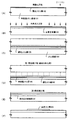
In this embodiment, a case where a single crystal silicon substrate whose main surface is a {110} plane is used for manufacturing an SOI substrate by the Smart-Cut method and a semiconductor device is manufactured using the SOI substrate will be described with reference to FIGS. To do.
まず、単結晶シリコン層の形成材料となる単結晶シリコン基板101を用意する。ここ
では主表面の結晶面が{110}面であるP型基板を用いるが、N型であっても良い。勿
論、単結晶シリコンゲルマニウム基板を用いることもできる。
First, a single crystal silicon substrate 101 which is a material for forming a single crystal silicon layer is prepared. Here, a P-type substrate having a {110} plane on the main surface is used, but an N-type substrate may be used. Of course, a single crystal silicon germanium substrate can also be used.
次いで熱酸化処理を行い、その主表面(素子形成面に相当する)に酸化シリコン膜10
2を形成する。膜厚は実施者が適宜決定すれば良いが、10〜500nm(代表的には20
〜50nm)とすれば良い。この酸化シリコン膜102は後にSOI基板の埋め込み絶縁層
の一部として機能する。(図1(A))
Next, thermal oxidation treatment is performed, and a silicon oxide film 10 is formed on the main surface (corresponding to the element formation surface).
2 is formed. The film thickness may be determined appropriately by the practitioner, but is 10 to 500 nm (typically 20
˜50 nm). This silicon oxide film 102 functions later as part of the buried insulating layer of the SOI substrate. (Fig. 1 (A))
この時、単結晶シリコン基板101と酸化シリコン膜102の界面の密着性は非常に高
いものとなる。これは本願発明では{110}面上に酸化シリコン膜102を形成するた
め、非常に整合性の高い界面が実現されるからである。この界面は最終的にTFTとなっ
た時、活性層と下地膜との界面であるため、密着性(整合性)が高いことは非常に有利で
ある。
At this time, the adhesion at the interface between the single crystal silicon substrate 101 and the silicon oxide film 102 is very high. This is because in the present invention, since the silicon oxide film 102 is formed on the {110} plane, a highly consistent interface is realized. Since this interface is the interface between the active layer and the base film when it finally becomes a TFT, it is very advantageous to have high adhesion (coherence).
また、酸化シリコン膜102の膜厚を20〜50nmと薄くすることが可能であるのは、
単結晶シリコン基板101の結晶面が{110}面であるため、薄くても密着性の高い酸
化シリコン膜が形成できるからである。
In addition, it is possible to reduce the thickness of the silicon oxide film 102 to 20 to 50 nm.
This is because the crystal plane of the single crystal silicon substrate 101 is the {110} plane, so that a silicon oxide film with high adhesion can be formed even if it is thin.
なお、{110}面は酸化反応が進行すると次第にシリコン表面のうねり(凹凸)が大
きくなるという問題があるが、本実施例の様に薄い酸化シリコン膜を設ける場合、酸化量
が小さいのでその様なうねりの問題を極力排除できる。このことは、本明細書に記載され
た全ての実施例に共通する利点である。
The {110} plane has a problem that the undulation (unevenness) of the silicon surface gradually increases as the oxidation reaction proceeds. However, when a thin silicon oxide film is provided as in this embodiment, the amount of oxidation is small, and so on. The problem of swell can be eliminated as much as possible. This is an advantage common to all the embodiments described herein.
従って、本願発明を用いて作製された単結晶シリコン層は極めて平坦な表面を有する。
例えば、うねりの頂点から頂点までの距離は、前述した{110}面に含まれる3つの原
子の隣接原子間距離の10倍以下(好ましくは20倍以下)である。即ち、約5nm以下(
好ましくは10nm以下)である。
Therefore, the single crystal silicon layer manufactured using the present invention has a very flat surface.
For example, the distance from the apex of the undulation to the apex is 10 times or less (preferably 20 times or less) the distance between adjacent atoms of three atoms included in the {110} plane described above. That is, about 5nm or less (
Preferably it is 10 nm or less.
次に、単結晶シリコン基板101の主表面側から酸化シリコン膜102を通して水素を
添加する。この場合、水素イオンの形でイオンインプランテーション法を用いて水素添加
を行えば良い。勿論、水素の添加工程を他の手段で行うことも可能である。こうして水素
含有層103が形成される。本実施例では水素イオンを1×10¹⁶〜1×10¹⁷atoms/cm
2のドーズ量で添加する。(図1(B))
Next, hydrogen is added from the main surface side of the single crystal silicon substrate 101 through the silicon oxide film 102. In this case, hydrogen may be added using an ion implantation method in the form of hydrogen ions. Of course, the hydrogen addition step can be performed by other means. Thus, the hydrogen-containing layer 103 is formed. In this embodiment, hydrogen ions are used in an amount of 1 × 10 16 to 1 × 10 17 atoms / cm.
Add at a dose of 2 . (Fig. 1 (B))
なお、水素含有層103が形成される深さは後に単結晶シリコン層の膜厚を決定するた
め、精密な制御が必要である。本実施例では単結晶シリコン基板101の主表面と水素含
有層103との間に50nm厚の単結晶シリコン層が残る様に水素添加プロファイルの深さ
方向の制御を行っている。
Note that the depth at which the hydrogen-containing layer 103 is formed needs to be precisely controlled because it determines the thickness of the single crystal silicon layer later. In this embodiment, the depth direction of the hydrogenation profile is controlled so that a 50 nm thick single crystal silicon layer remains between the main surface of the single crystal silicon substrate 101 and the hydrogen-containing layer 103.
また、{110}面は原子密度が最も小さな面であるため、水素イオンを添加してもシ
リコン原子との衝突確率が最も小さい。即ち、イオン添加する際のダメージを最小限に抑
えることが可能である。
Moreover, since the {110} plane has the lowest atomic density, the collision probability with the silicon atom is the lowest even when hydrogen ions are added. That is, it is possible to minimize damage when adding ions.
次に、単結晶シリコン基板101と支持基板とを貼り合わせる。本実施例では支持基板
としてシリコン基板104を用い、その表面には貼り合わせ用の酸化シリコン膜105を
設けておく。なお、シリコン基板104としてはFZ法で形成された安価なシリコン基板
を用意すれば十分である。勿論、多結晶シリコン基板であっても構わない。また、平坦性
さえ確保できれば石英基板、セラミックス基板、結晶化ガラス基板などの高耐熱性基板を
用いても良い。(図1(C))
Next, the single crystal silicon substrate 101 and the supporting substrate are attached to each other. In this embodiment, a silicon substrate 104 is used as a support substrate, and a silicon oxide film 105 for bonding is provided on the surface thereof. Note that it is sufficient to prepare an inexpensive silicon substrate formed by the FZ method as the silicon substrate 104. Of course, it may be a polycrystalline silicon substrate. Further, a high heat resistant substrate such as a quartz substrate, a ceramic substrate, or a crystallized glass substrate may be used as long as flatness can be ensured. (Figure 1 (C))
この時、貼り合わせ界面は親水性の高い酸化シリコン膜同士となるので、両表面に含ま
れた水分の反応により水素結合で接着される。
At this time, since the bonding interface is made of silicon oxide films having high hydrophilicity, they are bonded by hydrogen bonds by the reaction of moisture contained on both surfaces.
次に、400〜600℃(典型的には500℃)の熱処理(第1熱処理)を行う。この
熱処理により水素含有層103では微小空乏の体積変化が起こり、水素含有層103に沿
って破断面が発生する。これにより単結晶シリコン基板101は分断され、支持基板の上
には酸化シリコン膜102と単結晶シリコン層106が残される。(図1(D))
Next, a heat treatment (first heat treatment) at 400 to 600 ° C. (typically 500 ° C.) is performed. By this heat treatment, a volume change of microdepletion occurs in the hydrogen-containing layer 103, and a fracture surface is generated along the hydrogen-containing layer 103. Thus, the single crystal silicon substrate 101 is divided, and the silicon oxide film 102 and the single crystal silicon layer 106 are left on the support substrate. (Figure 1 (D))
次に、第2熱処理工程として1050〜1150℃の温度範囲でファーネスアニール工
程を行う。この工程では貼り合わせ界面において、Si-O-Si結合の応力緩和が起こり、貼
り合わせ界面が安定化する。即ち、単結晶シリコン層106を支持基板上に完全に接着さ
せるための工程となる。本実施例ではこの工程を1100℃、2時間で行う。
Next, a furnace annealing step is performed in a temperature range of 1050 to 1150 ° C. as a second heat treatment step. In this step, stress relaxation of the Si—O—Si bond occurs at the bonding interface, and the bonding interface is stabilized. That is, this is a process for completely bonding the single crystal silicon layer 106 on the supporting substrate. In this embodiment, this step is performed at 1100 ° C. for 2 hours.
こうして貼り合わせ界面が安定化することで埋め込み絶縁層107が画定する。なお、
図1(E)において埋め込み絶縁層107中の点線は、貼り合わせ界面を示しており、界
面が強固に接着されたことを意味している。
Thus, the embedded insulating layer 107 is defined by stabilizing the bonding interface. In addition,
In FIG. 1E, a dotted line in the buried insulating layer 107 indicates a bonding interface, which means that the interface is firmly bonded.
次に、単結晶シリコン層106の表面を平坦化する。平坦化にはCMP(ケミカルメカ
ニカルポリッシング)と呼ばれる研磨工程や還元雰囲気中で高温(900〜1200℃程
度)のファーネスアニール処理を行えば良い。
Next, the surface of the single crystal silicon layer 106 is planarized. For planarization, a high temperature (about 900 to 1200 ° C.) furnace annealing treatment may be performed in a polishing process called CMP (Chemical Mechanical Polishing) or in a reducing atmosphere.
最終的な単結晶シリコン層106の膜厚は10〜200nm(好ましくは20〜100nm
)とすれば良い。
The final thickness of the single crystal silicon layer 106 is 10 to 200 nm (preferably 20 to 100 nm).
).
次に、単結晶シリコン層106をパターニングして、後にTFTの活性層となる島状シ
リコン層108を形成する。なお、本実施例では一つの島状シリコン層しか記載していな
いが、同一基板上に複数個が形成される。(図1(F))
Next, the single crystal silicon layer 106 is patterned to form an island-like silicon layer 108 that will later become an active layer of the TFT. Although only one island-like silicon layer is shown in this embodiment, a plurality of silicon layers are formed on the same substrate. (Fig. 1 (F))
以上の様にして、主表面が{110}面である島状シリコン層108が得られる。本願
発明はこうして得られた島状シリコン層をTFTの活性層として用い、同一基板上に複数
のTFTを形成することに特徴がある。
As described above, the island-like silicon layer 108 whose main surface is the {110} plane is obtained. The present invention is characterized in that the island-like silicon layer thus obtained is used as an active layer of a TFT and a plurality of TFTs are formed on the same substrate.
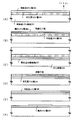
次に、TFTの形成方法について図2を用いて説明する。まず、図1(F)の状態まで
を完成させる。なお、図2(A)において、支持基板201は実際には図1のシリコン基
板104と埋め込み絶縁層107とに区別されるが、簡易的に一体化した状態で示す。ま
た、図2(A)の島状シリコン層202が図1(F)
の島状シリコン層108に相当する。
Next, a method for forming a TFT will be described with reference to FIGS. First, the state up to the state of FIG. In FIG. 2A, the support substrate 201 is actually divided into the silicon substrate 104 and the embedded insulating layer 107 in FIG. In addition, the island-shaped silicon layer 202 in FIG.
Corresponds to the island-like silicon layer 108.
次に、熱酸化工程を行って島状シリコン層202の表面に10nm厚の酸化シリコン膜2
03を形成する。この酸化シリコン膜203はゲート絶縁膜として機能する。ゲート絶縁
膜203を形成したら、その上に導電性を有するポリシリコン膜を形成し、パターニング
によりゲート配線204を形成する。(図2(A))
Next, a silicon oxide film 2 having a thickness of 10 nm is formed on the surface of the island-like silicon layer 202 by performing a thermal oxidation process.
03 is formed. This silicon oxide film 203 functions as a gate insulating film. After the gate insulating film 203 is formed, a conductive polysilicon film is formed thereon, and a gate wiring 204 is formed by patterning. (Fig. 2 (A))
なお、本実施例ではゲート配線としてN型導電性を持たせたポリシリコン膜を利用する
が、材料はこれに限定されるものではない。特に、ゲート配線の抵抗を下げるにはタンタ
ル、タンタル合金又はタンタルと窒化タンタルとの積層膜等の金属膜を用いることも有効
である。さらに低抵抗なゲート配線を狙うならば銅や銅合金を用いても有効である。
In this embodiment, a polysilicon film having N-type conductivity is used as the gate wiring, but the material is not limited to this. In particular, it is effective to use a metal film such as tantalum, a tantalum alloy, or a laminated film of tantalum and tantalum nitride in order to reduce the resistance of the gate wiring. Furthermore, if a low resistance gate wiring is aimed, it is effective to use copper or a copper alloy.
図2(A)の状態が得られたら、N型導電性又はP型導電性を付与する不純物を添加し
て不純物領域205を形成する。この時の不純物濃度で後にLDD領域の不純物濃度が決
定する。本実施例では1×10¹⁸atoms/cm3の濃度で砒素を添加するが、不純物も濃度も
本実施例に限定される必要はない。
When the state of FIG. 2A is obtained, an impurity region 205 is formed by adding an impurity imparting N-type conductivity or P-type conductivity. The impurity concentration in the LDD region is determined later by the impurity concentration at this time. In this embodiment, arsenic is added at a concentration of 1 × 10 18 atoms / cm 3 , but neither the impurity nor the concentration need be limited to this embodiment.
次に、ゲート配線の表面に5〜10nm程度の薄い酸化シリコン膜206を形成する。こ
れは熱酸化法やプラズマ酸化法を用いて形成すれば良い。この酸化シリコン膜206の形
成には、次のサイドウォール形成工程でエッチングストッパーとして機能させる目的があ
る。
Next, a thin silicon oxide film 206 of about 5 to 10 nm is formed on the surface of the gate wiring. This may be formed using a thermal oxidation method or a plasma oxidation method. The formation of the silicon oxide film 206 has the purpose of functioning as an etching stopper in the next side wall formation step.
エッチングストッパーとなる酸化シリコン膜206を形成したら、窒化シリコン膜を形
成してエッチバックを行い、サイドウォール207を形成する。こうして図2(B)の状
態を得る。
After the silicon oxide film 206 serving as an etching stopper is formed, a silicon nitride film is formed and etched back to form sidewalls 207. In this way, the state of FIG.
なお、本実施例ではサイドウォール207として窒化シリコン膜を用いたが、ポリシリ
コン膜やアモルファスシリコン膜を用いることもできる。勿論、ゲート配線の材料が変わ
れば、それに応じてサイドウォールとして用いることのできる材料の選択幅も広がること
は言うまでもない。
In this embodiment, a silicon nitride film is used as the sidewall 207, but a polysilicon film or an amorphous silicon film can also be used. Of course, if the material of the gate wiring changes, it goes without saying that the range of selection of materials that can be used as sidewalls also increases accordingly.
次に、再び先程と同一導電型の不純物を添加する。この時に添加する不純物濃度は先程
の工程よりも高い濃度とする。本実施例では不純物として砒素を用い、濃度は1×10²¹
atoms/cm3とするがこれに限定する必要はない。この不純物の添加工程によりソース領域
208、ドレイン領域209、LDD領域210及びチャネル形成領域211が画定する
。(図2(C))
Next, an impurity having the same conductivity type as before is added again. The impurity concentration added at this time is higher than that in the previous step. In this embodiment, arsenic is used as an impurity, and the concentration is 1 × 10 21.
It is not limited to atoms / cm 3 . The source region 208, the drain region 209, the LDD region 210, and the channel formation region 211 are defined by this impurity addition step. (Fig. 2 (C))
こうして各不純物領域が形成されたらファーネスアニール、レーザーアニール又はラン
プアニール等の手段により不純物の活性化を行う。
When each impurity region is thus formed, the impurity is activated by means such as furnace annealing, laser annealing or lamp annealing.
次に、ゲート配線204、ソース領域208及びドレイン領域209の表面に形成され
た酸化シリコン膜を除去し、それらの表面を露呈させる。そして、5nm程度のコバルト膜
212を形成して熱処理工程を行う。この熱処理によりコバルトとシリコンとの反応が起
こり、シリサイド層(コバルトシリサイド層)213が形成される。(図2(D))
Next, the silicon oxide film formed on the surfaces of the gate wiring 204, the source region 208, and the drain region 209 is removed to expose the surfaces. Then, a cobalt film 212 of about 5 nm is formed and a heat treatment process is performed. By this heat treatment, a reaction between cobalt and silicon occurs, and a silicide layer (cobalt silicide layer) 213 is formed. (Fig. 2 (D))
この技術は公知のサリサイド技術である。従って、コバルトの代わりにチタンやタング
ステンを用いても構わないし、熱処理条件等は公知技術を参考にすれば良い。本実施例で
はランプアニールを用いて熱処理工程を行う。
This technique is a known salicide technique. Therefore, titanium or tungsten may be used instead of cobalt, and heat treatment conditions may be referred to known techniques. In this embodiment, the heat treatment process is performed using lamp annealing.
こうしてシリサイド層213を形成したら、コバルト膜212を除去する。その後、1
μm厚の層間絶縁膜214を形成する。層間絶縁膜214としては、酸化シリコン膜、窒
化シリコン膜もしくは酸化窒化シリコン膜などの無機絶縁膜又はポリイミド、アクリル、
ポリアミド、ポリイミドアミド、BCB(ベンゾシクロブテン)などの有機樹脂絶縁膜を
用いれば良い。また、これらの無機絶縁膜または有機樹脂絶縁膜を積層しても良い。
When the silicide layer 213 is thus formed, the cobalt film 212 is removed. Then 1
An interlayer insulating film 214 having a thickness of μm is formed. As the interlayer insulating film 214, an inorganic insulating film such as a silicon oxide film, a silicon nitride film, or a silicon oxynitride film, polyimide, acrylic,
An organic resin insulating film such as polyamide, polyimide amide, or BCB (benzocyclobutene) may be used. Further, these inorganic insulating films or organic resin insulating films may be stacked.
次に、層間絶縁膜214にコンタクトホールを形成してアルミニウムを主成分とする材
料でなるソース配線215及びドレイン配線216を形成する。最後に素子全体に対して
水素雰囲気中で300℃2時間のファーネスアニールを行い、水素化を完了する。
Next, contact holes are formed in the interlayer insulating film 214 to form source wirings 215 and drain wirings 216 made of a material containing aluminum as a main component. Finally, furnace annealing is performed on the entire device in a hydrogen atmosphere at 300 ° C. for 2 hours to complete the hydrogenation.
こうして、図2(E)に示す様なTFTが得られる。なお、本実施例で説明した構造は
一例であって本願発明を適用しうるTFT構造はこれに限定されない。
従って、公知のあらゆる構造のTFTに対して適用可能である。また、本実施例の工程条
件は一例であり、本願発明の本質部分以外は実施者が適宜最適な条件を設定すれば良い。
In this way, a TFT as shown in FIG. 2E is obtained. Note that the structure described in this embodiment is merely an example, and the TFT structure to which the present invention can be applied is not limited thereto.
Therefore, it can be applied to TFTs having any known structure. Moreover, the process conditions of a present Example are an example, A practitioner should just set optimal conditions suitably except the essential part of this invention.
また、本実施例ではNチャネル型TFTを例にとって説明したが、Pチャネル型TFT
を作製することも容易である。さらに同一基板上にNチャネル型TFTとPチャネル型T
FTとを形成して相補的に組み合わせ、CMOS回路を形成することも可能である。
In this embodiment, an N-channel TFT has been described as an example.
It is also easy to produce. Furthermore, N-channel TFT and P-channel T on the same substrate
It is also possible to form an FT and complementarily combine to form a CMOS circuit.
さらに、図2(E)の構造においてドレイン配線216と電気的に接続する画素電極(
図示せず)を公知の手段で形成すればアクティブマトリクス型表示装置の画素スイッチン
グ素子を形成することも容易である。
Further, in the structure of FIG. 2E, a pixel electrode (which is electrically connected to the drain wiring 216)
It is also easy to form a pixel switching element of an active matrix display device if it is formed by a known means.
即ち、本願発明は液晶表示装置、EL(エレクトロルミネッセンス)表示装置、EC(
エレクトロクロミクス)表示装置又は光電変換装置(光センサ)等に代表される電気光学
装置の作製方法としても非常に有効な技術である。
That is, the present invention is a liquid crystal display device, an EL (electroluminescence) display device, an EC (
This is a very effective technique as a method for manufacturing an electro-optical device typified by an electrochromic display device or a photoelectric conversion device (photosensor).
本願発明では、主表面が{110}面である単結晶シリコン基板を用いて実施例1とは
異なるSOI基板を作製し、それを用いて半導体装置を作製した場合例について説明する
。具体的にはELTRANと呼ばれる技術を用いる場合を説明する。
In the present invention, an example will be described in which an SOI substrate different from that in Example 1 is manufactured using a single crystal silicon substrate having a {110} plane as a main surface, and a semiconductor device is manufactured using the SOI substrate. Specifically, a case where a technique called ELTRAN is used will be described.
まず、主表面(結晶面)が{110}面である単結晶シリコン基板301を用意する。
次に、その主表面を陽極化成することにより多孔質シリコン層302を形成する。陽極化
成工程はフッ酸とエタノールの混合溶液中で行えば良い。多孔質シリコン層302は柱状
の表面孔が表面密度にして1011個/cm3程度設けられた単結晶シリコン層と考えられ、単
結晶シリコン基板301の結晶状態(配向性等)をそのまま受け継ぐ。なお、ELTRA
N法自体が公知であるので詳細な説明はここでは省略する。
First, a single crystal silicon substrate 301 whose main surface (crystal plane) is a {110} plane is prepared.
Next, the porous silicon layer 302 is formed by anodizing the main surface. The anodizing step may be performed in a mixed solution of hydrofluoric acid and ethanol. The porous silicon layer 302 is considered to be a single crystal silicon layer in which columnar surface holes are provided with a surface density of about 10 11 pieces / cm 3 , and inherits the crystal state (orientation, etc.) of the single crystal silicon substrate 301 as it is. ELTRA
Since the N method itself is known, a detailed description is omitted here.
そして、その多孔質シリコン層302を形成したら、還元雰囲気中で900〜1200
℃(好ましくは1000〜1150℃)の温度範囲の熱処理工程を行ことが好ましい。本
実施例では水素雰囲気中で1050℃、2時間の加熱処理を行う。
When the porous silicon layer 302 is formed, 900 to 1200 in a reducing atmosphere.
It is preferable to perform a heat treatment step in a temperature range of ° C (preferably 1000 to 1150 ° C). In this embodiment, heat treatment is performed at 1050 ° C. for 2 hours in a hydrogen atmosphere.
還元雰囲気としては水素雰囲気、アンモニア雰囲気、水素又はアンモニアを含む不活性
雰囲気(水素と窒素又は水素とアルゴンの混合雰囲気など)が望ましいが、不活性雰囲気
でも結晶性珪素膜の表面の平坦化は可能である。しかし、還元作用を利用して自然酸化膜
の還元を行うとエネルギーの高いシリコン原子が多く発生し、結果的に平坦化効果が高ま
るので好ましい。
The reducing atmosphere is preferably a hydrogen atmosphere, an ammonia atmosphere, or an inert atmosphere containing hydrogen or ammonia (such as a mixed atmosphere of hydrogen and nitrogen or hydrogen and argon), but the surface of the crystalline silicon film can be planarized even in an inert atmosphere. It is. However, it is preferable to reduce the natural oxide film by using the reducing action because many silicon atoms with high energy are generated and as a result, the planarization effect is enhanced.
ただし、特に注意が必要なのは雰囲気中に含まれる酸素又は酸素化合物(例えばOH基
)の濃度を10ppm以下(好ましくは1ppm以下)にしておくことである。さもないと水素
による還元反応が起こらなくなってしまう。
However, it is particularly necessary to keep the concentration of oxygen or oxygen compounds (for example, OH groups) in the atmosphere at 10 ppm or less (preferably 1 ppm or less). Otherwise, the hydrogen reduction reaction will not occur.
この時、多孔質シリコン層302の表面近傍では表面孔がシリコン原子の移動によって
閉塞され、非常に平坦なシリコン表面が得られる。
At this time, in the vicinity of the surface of the porous silicon layer 302, the surface holes are blocked by the movement of silicon atoms, and a very flat silicon surface is obtained.
次に、多孔質シリコン層302上に単結晶シリコン層303をエピタキシャル成長させ
る。この時、エピタキシャル成長させた単結晶シリコン層303は単結晶シリコン基板3
01の結晶構造をそのまま反映するので、主表面が{110}面となる。また、膜厚は1
0〜200nm(好ましくは20〜100nm)とすれば良い。(図3(A))
Next, the single crystal silicon layer 303 is epitaxially grown on the porous silicon layer 302. At this time, the epitaxially grown single crystal silicon layer 303 is converted into a single crystal silicon substrate 3.
Since the crystal structure of 01 is reflected as it is, the main surface becomes the {110} plane. The film thickness is 1
The thickness may be 0 to 200 nm (preferably 20 to 100 nm). (Fig. 3 (A))
次に、単結晶シリコン層303を酸化して酸化シリコン層304を形成する。
形成方法としては、熱酸化、プラズマ酸化、レーザー酸化などを用いることが可能である
。このとき、単結晶シリコン層305が残存する。(図3(B))
Next, the single crystal silicon layer 303 is oxidized to form a silicon oxide layer 304.
As a formation method, thermal oxidation, plasma oxidation, laser oxidation, or the like can be used. At this time, the single crystal silicon layer 305 remains. (Fig. 3 (B))
次に、支持基板として表面に酸化シリコン層を設けた多結晶シリコン基板306を用意
する。勿論、表面に絶縁膜を設けたセラミックス基板、石英基板、ガラスセラミックス基
板を用いても良い。
Next, a polycrystalline silicon substrate 306 having a silicon oxide layer on the surface is prepared as a support substrate. Of course, a ceramic substrate, a quartz substrate, or a glass ceramic substrate provided with an insulating film on the surface may be used.
こうして単結晶シリコン基板301と支持基板(多結晶シリコン基板306)の準備が
完了したら、互いの主表面を向かい合わせる形で両基板を貼り合わせる。この場合、互い
の基板に設けられた酸化シリコン層が接着剤の役目を果たす。
(図3(C))
When the preparation of the single crystal silicon substrate 301 and the support substrate (polycrystalline silicon substrate 306) is thus completed, the two substrates are bonded together so that their main surfaces face each other. In this case, the silicon oxide layers provided on the substrates serve as an adhesive.
(Fig. 3 (C))
貼り合わせが終了したら、次に1050〜1150℃の温度で熱処理工程を行い、酸化
シリコン同士でなる貼り合わせ界面の安定化を行う。本実施例ではこの熱処理工程を11
00℃、2時間で行う。なお、図3(C)において点線で示されているのは完全に接着さ
れた貼り合わせ界面である。また、両基板に設けられた酸化シリコン層は熱処理により一
体化して埋め込み絶縁層307となる。
When the bonding is completed, a heat treatment step is then performed at a temperature of 1050 to 1150 ° C. to stabilize the bonding interface made of silicon oxides. In this embodiment, this heat treatment step is performed as 11.
Perform at 00 ° C. for 2 hours. Note that in FIG. 3C, a dotted line indicates a completely bonded bonding interface. Further, the silicon oxide layers provided on both the substrates are integrated by heat treatment to form a buried insulating layer 307.
次に、CMP等の機械的な研磨により単結晶シリコン基板301を裏面側から研削し、
多孔質シリコン層302が露呈したところで研削工程を終了する。こうして図3(D)の
状態を得る。
Next, the single crystal silicon substrate 301 is ground from the back side by mechanical polishing such as CMP,
The grinding process is terminated when the porous silicon layer 302 is exposed. In this way, the state of FIG.
次に、多孔質シリコン層302をウェットエッチングして選択的に除去する。
用いるエッチャントはフッ酸水溶液と過酸化水素水溶液との混合溶液が良い。49%HF
と30%H2O2を1:5で混合した溶液は、単結晶シリコン層と多孔質シリコン層との間
で10万倍以上の選択比を持つことが報告されている。
Next, the porous silicon layer 302 is selectively removed by wet etching.
The etchant used is preferably a mixed solution of a hydrofluoric acid aqueous solution and a hydrogen peroxide aqueous solution. 49% HF
And a 30% H 2 O 2 mixed solution of 1: 5 have been reported to have a selectivity ratio of 100,000 times or more between the single crystal silicon layer and the porous silicon layer.
こうして図3(E)の状態が得られる。この状態では多結晶シリコン基板306上に埋
め込み絶縁層307が設けられ、その上に単結晶シリコン層308が形成されている。
In this way, the state of FIG. In this state, a buried insulating layer 307 is provided on the polycrystalline silicon substrate 306, and a single crystal silicon layer 308 is formed thereon.
この時点でSOI基板は完成しているのだが、単結晶シリコン層308の表面には微小
な凹凸が存在するので、水素雰囲気中で熱処理工程を行い、平坦化を施すことが望ましい
。この平坦化現象は前述した様に自然酸化膜を還元することによるシリコン原子の増速表
面拡散によるものである。
Although the SOI substrate is completed at this point, since there are minute irregularities on the surface of the single crystal silicon layer 308, it is desirable to perform planarization by performing a heat treatment step in a hydrogen atmosphere. As described above, this flattening phenomenon is due to accelerated surface diffusion of silicon atoms by reducing the natural oxide film.
なおこの時、水素原子によって単結晶シリコン層308中に含まれるボロン(P型シリ
コン基板に含まれていたもの)が気相中へと離脱する効果もあるので不純物の低減にも有
効である。
Note that at this time, boron atoms contained in the single crystal silicon layer 308 by hydrogen atoms (what was contained in the P-type silicon substrate) are also released into the gas phase, which is effective in reducing impurities.
次に、得られた単結晶シリコン層308をパターニングして島状シリコン層309を形
成する。なお、図面上では一つしか記載していないが、複数個を形成しても良いことは言
うまでもない。
Next, the obtained single crystal silicon layer 308 is patterned to form an island-shaped silicon layer 309. Although only one is shown in the drawing, it goes without saying that a plurality may be formed.
この後は、実施例1において図2を用いて説明したのと同様の工程によってTFTを作
製することができる。また、他の公知の手段を用いてTFTを形成しても良い。本実施例
では詳細な説明を省略する。
Thereafter, a TFT can be manufactured by the same process as that described in
本願発明では、主表面が{110}面である単結晶シリコン基板を用いて実施例1、実
施例2とは異なるSOI基板を作製し、それを用いて半導体装置を作製した場合例につい
て説明する。具体的にはSIMOXと呼ばれるSOI基板を作製する場合を説明する。
In the present invention, an example will be described in which an SOI substrate different from those in
図4(A)において、401は単結晶シリコン基板である。本実施例では、まず単結晶
シリコン基板401に対して酸素イオンを添加し、所定の深さに酸素含有層402を形成
する。酸素イオンは1×10¹⁸atoms/cm2程度のドーズ量で添加すれば良い。
In FIG. 4A, reference numeral 401 denotes a single crystal silicon substrate. In this embodiment, first, oxygen ions are added to the single crystal silicon substrate 401 to form an oxygen-containing layer 402 at a predetermined depth. Oxygen ions may be added at a dose of about 1 × 10 18 atoms / cm 2 .
また、この時、{110}面は原子密度が小さいため、酸素イオンとシリコン原子との
衝突確率は小さいものとなる。即ち、酸素を添加することによるシリコン表面のダメージ
を最小限に抑えることができる。勿論、イオン添加中に基板温度を400〜600℃にす
ることでさらにダメージを低減することができる。
At this time, since the {110} plane has a low atomic density, the collision probability between oxygen ions and silicon atoms is low. That is, damage to the silicon surface due to the addition of oxygen can be minimized. Of course, damage can be further reduced by setting the substrate temperature to 400 to 600 ° C. during ion addition.
次に、800〜1200℃の温度で熱処理を行い、酸素含有層402を埋め込み絶縁層
403に変化させる。酸素含有層402の深さ方向の幅はイオン添加時の酸素イオンの分
布で決まっており、裾をひくような分布を持っているが、この熱処理工程により単結晶シ
リコン基板401と埋め込み絶縁層403との界面は非常に急峻なものとなる。(図4(
B))
Next, heat treatment is performed at a temperature of 800 to 1200 ° C. to change the oxygen-containing layer 402 into the buried insulating layer 403. The width in the depth direction of the oxygen-containing layer 402 is determined by the distribution of oxygen ions at the time of ion addition, and has a distribution that has a skirt, but by this heat treatment process, the single crystal silicon substrate 401 and the buried insulating layer 403 The interface with is very steep. (Fig. 4 (
B))
この埋め込み絶縁層403の膜厚は10〜500nm(代表的には20〜50nm)とする
。20〜50nmといった薄い埋め込み絶縁層を実現できるのは単結晶シリコン基板401
と埋め込み絶縁層403の界面が安定に接合されているからであり、それは主表面が{1
10}面である単結晶シリコン基板を単結晶シリコン層の形成材料として用いるからに他
ならない。
The buried insulating layer 403 has a thickness of 10 to 500 nm (typically 20 to 50 nm). A single buried silicon layer 401 can realize a thin buried insulating layer of 20 to 50 nm.
And the buried insulating layer 403 are stably bonded to each other because the main surface is {1
This is because the single crystal silicon substrate having the 10} plane is used as the material for forming the single crystal silicon layer.
こうして埋め込み絶縁層403が形成されると、埋め込み絶縁層403の上には単結晶
シリコン層404が残存する。即ち、本実施例では主表面が{110}面である単結晶シ
リコン基板を用いるため、埋め込み絶縁層を形成した後に得られる単結晶シリコン層40
4も主表面(結晶面)が{110}面となる。なお、単結晶シリコン層404の膜厚は1
0〜200nm(好ましくは20〜100nm)
となる様に調節すれば良い。
When the buried insulating layer 403 is formed in this way, the single crystal silicon layer 404 remains on the buried insulating layer 403. That is, in this embodiment, since a single crystal silicon substrate having a main surface of {110} plane is used, the single crystal silicon layer 40 obtained after the buried insulating layer is formed.
4, the main surface (crystal plane) is the {110} plane. Note that the thickness of the single crystal silicon layer 404 is 1
0 to 200 nm (preferably 20 to 100 nm)
You just have to adjust it.
こうして単結晶シリコン層404が得られたら、パターニングして島状シリコン層40
5を得る。島状シリコン層は複数形成しても構わない。
When the single crystal silicon layer 404 is obtained in this way, the island-like silicon layer 40 is patterned by patterning.
Get 5. A plurality of island-like silicon layers may be formed.
この後は、実施例1において図2で説明した工程に従って複数のTFTを完成すれば良
い。また、他の公知の手段を用いてTFTを形成しても良い。本実施例では詳細な説明を
省略する。
Thereafter, a plurality of TFTs may be completed according to the process described in
本実施例では、本願発明の半導体装置として反射型液晶表示装置の例を図5に示す。画
素TFT(画素スイッチング素子)の作製方法やセル組工程は公知の手段を用いれば良い
ので詳細な説明は省略する。
In this embodiment, an example of a reflective liquid crystal display device is shown in FIG. 5 as a semiconductor device of the present invention. Since a known method may be used for a manufacturing method of a pixel TFT (pixel switching element) and a cell assembly process, detailed description thereof is omitted.
図5(A)において11は絶縁表面を有する基板、12は画素マトリクス回路、13は
ソースドライバー回路、14はゲイトドライバー回路、15は対向基板、16はFPC(
フレキシブルプリントサーキット)、17は信号処理回路である。信号処理回路17とし
ては、D/Aコンバータ、γ補正回路、信号分割回路などの従来ICで代用していた様な
処理を行う回路を形成することができる。勿論、ガラス基板上にICチップを設けて、I
Cチップ上で信号処理を行うことも可能である。
In FIG. 5A, 11 is a substrate having an insulating surface, 12 is a pixel matrix circuit, 13 is a source driver circuit, 14 is a gate driver circuit, 15 is a counter substrate, and 16 is an FPC (FPC).
17 is a signal processing circuit. As the
It is also possible to perform signal processing on the C chip.
さらに、本実施例では液晶表示装置を例に挙げて説明しているが、アクティブマトリク
ス型の表示装置であればEL(エレクトロルミネッセンス)表示装置やEC(エレクトロ
クロミックス)表示装置などの他の電気光学装置に本願発明を用いることも可能である。
Further, in this embodiment, the liquid crystal display device is described as an example. However, if the display device is an active matrix type, other electric devices such as an EL (electroluminescence) display device and an EC (electrochromic) display device are used. The present invention can also be used for an optical device.
ここで図5(A)のドライバー回路13、14を構成する回路の一例を図5(B)に示
す。なお、TFT部分については既に実施例1で説明しているので、ここでは必要箇所の
みの説明を行うこととする。
Here, FIG. 5B shows an example of a circuit constituting the
図5(B)において、501、502はNチャネル型TFT、503はPチャネル型T
FTであり、501と503のTFTでCMOS回路を構成している。
504は窒化シリコン膜/酸化シリコン膜/樹脂膜の積層膜でなる絶縁層、その上にはチ
タン配線505が設けられ、前述のCMOS回路とTFT502とが電気的に接続されて
いる。チタン配線はさらに樹脂膜でなる絶縁層506で覆われている。二つの絶縁層50
4、506は平坦化膜としての機能も有している。
In FIG. 5B, 501 and 502 are N-channel TFTs, and 503 is a P-channel T.
It is an FT, and a CMOS circuit is composed of TFTs 501 and 503.
Reference numeral 504 denotes an insulating layer formed of a laminated film of silicon nitride film / silicon oxide film / resin film, and a titanium wiring 505 is provided on the insulating layer, and the above-described CMOS circuit and the TFT 502 are electrically connected. The titanium wiring is further covered with an insulating layer 506 made of a resin film. Two insulating layers 50
4 and 506 also have a function as a planarizing film.
また、図5(A)の画素マトリクス回路12を構成する回路の一部を図5(C)に示す
。図5(C)において、507はダブルゲート構造のNチャネル型TFTでなる画素TF
Tであり、画素領域内に大きく広がる様にしてドレイン配線508が形成されている。
FIG. 5C illustrates part of a circuit included in the
The drain wiring 508 is formed so as to extend widely in the pixel region.
その上には絶縁層504が設けられ、その上にチタン配線505が設けられている。こ
の時、絶縁層504の一部には凹部が落とし込み部が形成され、最下層の窒化シリコン及
び酸化シリコンのみが残される。これによりドレイン配線508とチタン配線505との
間で補助容量が形成される。
An insulating layer 504 is provided thereon, and a titanium wiring 505 is provided thereon. At this time, a recess is dropped into a part of the insulating layer 504, and only the lowermost silicon nitride and silicon oxide are left. As a result, an auxiliary capacitance is formed between the drain wiring 508 and the titanium wiring 505.
また、画素マトリクス回路内に設けられたチタン配線505はソース・ドレイン配線と
後の画素電極との間において電界遮蔽効果をもたらす。さらに、複数設けられた画素電極
間の隙間ではブラックマスクとしても機能する。
The titanium wiring 505 provided in the pixel matrix circuit provides an electric field shielding effect between the source / drain wiring and the subsequent pixel electrode. Further, it functions as a black mask in the gaps between a plurality of pixel electrodes.
そして、チタン配線505を覆って絶縁層506が設けられ、その上に反射性導電膜で
なる画素電極509が形成される。勿論、画素電極509の表面に反射率を上げるための
工夫をなしても構わない。
An insulating layer 506 is provided to cover the titanium wiring 505, and a pixel electrode 509 made of a reflective conductive film is formed thereon. Of course, the surface of the pixel electrode 509 may be devised to increase the reflectance.
また、実際には画素電極509の上に配向膜や液晶層が設けられるが、ここでの説明は
省略する。
In addition, an alignment film and a liquid crystal layer are actually provided on the pixel electrode 509, but description thereof is omitted here.
本願発明を用いて以上の様な構成でなる反射型液晶表示装置を作製することができる。
勿論、公知の技術と組み合わせれば容易に透過型液晶表示装置(但し、支持基板として透
光性基板を用いた場合に限る)を作製することもできる。さらに、公知の技術と組み合わ
せればアクティブマトリクス型のEL表示装置も容易に作製することができる。
A reflection type liquid crystal display device having the above-described configuration can be manufactured using the present invention.
Needless to say, a transmissive liquid crystal display device (however, only when a light-transmitting substrate is used as a supporting substrate) can be easily manufactured by combining with a known technique. Further, an active matrix EL display device can be easily manufactured by combining with a known technique.
なお、本実施例の電気光学装置を作製するにあたって、実施例1〜実施例3のいずれの
SOI基板を用いても構わない。
In manufacturing the electro-optical device of this example, any of the SOI substrates of Examples 1 to 3 may be used.
本願発明は従来のIC技術全般に適用することが可能である。即ち、現在市場に流通し
ている全ての半導体回路に適用できる。例えば、ワンチップ上に集積化されたRISCプ
ロセッサ、ASICプロセッサ等のマイクロプロセッサに適用しても良いし、D/Aコン
バータ等の信号処理回路から携帯機器(携帯電話、PHS、モバイルコンピュータ)用の
高周波回路に適用しても良い。
The present invention can be applied to all conventional IC technologies. That is, it can be applied to all semiconductor circuits currently on the market. For example, the present invention may be applied to a microprocessor such as a RISC processor or an ASIC processor integrated on a single chip, or from a signal processing circuit such as a D / A converter to a portable device (cell phone, PHS, mobile computer). You may apply to a high frequency circuit.
図6に示すのは、マイクロプロセッサの一例である。マイクロプロセッサは典型的には
CPUコア21、RAM22、クロックコントローラ23、キャッシュメモリー24、キ
ャッシュコントローラ25、シリアルインターフェース26、I/Oポート27等から構
成される。
FIG. 6 shows an example of a microprocessor. The microprocessor typically includes a CPU core 21, a RAM 22, a clock controller 23, a cache memory 24, a cache controller 25, a serial interface 26, an I / O port 27, and the like.
勿論、図6に示すマイクロプロセッサは簡略化した一例であり、実際のマイクロプロセ
ッサはその用途によって多種多様な回路設計が行われる。
Needless to say, the microprocessor illustrated in FIG. 6 is a simplified example, and various circuit designs are performed on an actual microprocessor depending on its application.
しかし、どの様な機能を有するマイクロプロセッサであっても中枢として機能するのは
IC(Integrated Circuit)28である。IC28は半導体チップ29上に形成された集
積化回路をセラミック等で保護した機能回路である。
However, it is an IC (Integrated Circuit) 28 that functions as the center of a microprocessor having any function. The IC 28 is a functional circuit in which an integrated circuit formed on the semiconductor chip 29 is protected with ceramic or the like.
そして、その半導体チップ29上に形成された集積化回路(半導体回路)を構成するの
が本願発明の構造を有するNチャネル型TFT30、Pチャネル型TFT31である。な
お、基本的な回路はCMOS回路を最小単位として構成することで消費電力を抑えること
ができる。
The N-channel TFT 30 and the P-channel TFT 31 having the structure of the present invention constitute an integrated circuit (semiconductor circuit) formed on the semiconductor chip 29. Note that power consumption can be suppressed by configuring a basic circuit with a CMOS circuit as a minimum unit.
また、本実施例に示したマイクロプロセッサは様々な電子機器に搭載されて中枢回路と
して機能する。代表的な電子機器としてはパーソナルコンピュータ、携帯型情報端末機器
、その他あらゆる家電製品が挙げられる。また、車両(自動車や電車等)の制御用コンピ
ュータなども挙げられる。
The microprocessor shown in this embodiment is mounted on various electronic devices and functions as a central circuit. Typical electronic devices include personal computers, portable information terminal devices, and all other home appliances. Further, a computer for controlling a vehicle (such as an automobile or a train) may be used.
なお、本実施例の半導体回路を作製するにあたって、実施例1〜実施例3のいずれのS
OI基板を用いても構わない。
In producing the semiconductor circuit of this example, any S of Examples 1 to 3 was used.
An OI substrate may be used.
実施例4に示した電気光学装置や実施例5に示した半導体回路は、様々な電子機器に用
いることができる。その様な電子機器としては、ビデオカメラ、デジタルカメラ、プロジ
ェクター、プロジェクションTV、TV用ディスプレイ、パーソナルコンピュータ用ディ
スプレイ、ゴーグル型ディスプレイ(ヘッドマウントディスプレイ)、カーナビゲーショ
ン、パーソナルコンピュータ、画像再生装置(DVDプレイヤー、CDプレイヤー、MD
プレイヤー等)、携帯情報端末(モバイルコンピュータ、携帯電話、電子書籍等)などが
挙げられる。それらの一例を図7に示す。
The electro-optical device shown in Embodiment 4 and the semiconductor circuit shown in Embodiment 5 can be used for various electronic devices. Such electronic devices include video cameras, digital cameras, projectors, projection TVs, TV displays, personal computer displays, goggle-type displays (head-mounted displays), car navigation systems, personal computers, and image playback devices (DVD players, CD player, MD
Players), portable information terminals (mobile computers, mobile phones, electronic books, etc.). An example of them is shown in FIG.
図7(A)は携帯電話であり、本体2001、音声出力部2002、音声入力部200
3、表示装置2004、操作スイッチ2005、アンテナ2006で構成される。本願発
明を音声出力部2002、音声入力部2003、表示装置2004やその他の信号制御回
路に適用することができる。
FIG. 7A illustrates a mobile phone, which includes a main body 2001, an audio output unit 2002, and an audio input unit 200.
3, a display device 2004, an
図7(B)はビデオカメラであり、本体2101、表示装置2102、音声入力部21
03、操作スイッチ2104、バッテリー2105、受像部2106で構成される。本願
発明を表示装置2102、音声入力部2103やその他の信号制御回路に適用することが
できる。
FIG. 7B illustrates a video camera, which includes a main body 2101, a display device 2102, and an audio input unit 21.
03, an
図7(C)はモバイルコンピュータ(モービルコンピュータ)であり、本体2201、
カメラ部2202、受像部2203、操作スイッチ2204、表示装置2205で構成さ
れる。本願発明は表示装置2205やその他の信号制御回路に適用できる。
FIG. 7C shows a mobile computer (mobile computer).
The camera unit 2202, the image receiving unit 2203, operation switches 2204, and a display device 2205 are included. The present invention can be applied to the display device 2205 and other signal control circuits.
図7(D)はパーソナルコンピュータであり、本体2301、受像部2302、表示装
置2303、キーボード2304等で構成される。本願発明は表示装置2304やその他
の信号制御回路に用いることができる。
FIG. 7D illustrates a personal computer, which includes a main body 2301, an image receiving portion 2302, a display device 2303, a
図7(E)はリア型プロジェクターであり、本体2401、光源2402、表示装置2
403、偏光ビームスプリッタ2404、リフレクター2405、2406、スクリーン
2407で構成される。本発明は表示装置2403やその他の信号制御回路に適用するこ
とができる。
FIG. 7E illustrates a rear projector, which includes a main body 2401, a light source 2402, and a display device 2.
403, a
図7(F)は電子書籍であり、本体2501、表示装置2502、2503、記憶媒体
2504、操作スイッチ2505、アンテナ2506で構成される。本発明は表示装置2
502、2503やその他の信号制御回路に適用することができる。
FIG. 7F illustrates an electronic book which includes a
The present invention can be applied to 502 and 2503 and other signal control circuits.
以上の様に、本願発明の適用範囲は極めて広く、あらゆる分野の電子機器に用いること
が可能である。
As described above, the application range of the present invention is extremely wide and can be used for electronic devices in various fields.
本実施例は、実施例2の変形例であり、図3のELTRAN法を用いる際に、多孔質シ
リコン層302の形成方法を改良した例を示す。
The present embodiment is a modification of the second embodiment, and shows an example in which the method for forming the porous silicon layer 302 is improved when the ELTRAN method of FIG. 3 is used.
図3(A)の工程ではフッ酸とエタノールの混合溶液中で陽極化成処理を行って多孔質
シリコン層302を形成している。このとき、陽極化成処理は一定の電流密度で行ってい
るが、本実施例では電流密度を陽極化成処理の途中で切り換えることを特徴とする。
In the step of FIG. 3A, the anodizing treatment is performed in a mixed solution of hydrofluoric acid and ethanol to form the porous silicon layer 302. At this time, the anodizing treatment is performed at a constant current density, but the present embodiment is characterized in that the current density is switched during the anodizing treatment.
具体的には、陽極化成処理の途中で与える電流密度を上げ、それまでに形成された多孔
質シリコン層(第1多孔質シリコン層)よりも個々の孔の径が大きい第2の多孔質シリコ
ン層を形成する。
Specifically, the current density applied during the anodizing treatment is increased, and the second porous silicon having larger individual pore diameters than the porous silicon layer (first porous silicon layer) formed so far. Form a layer.
本実施例の場合、図3(C)の状態の多孔質シリコン層(第1多孔質シリコン層と第2
多孔質シリコン層との積層体)に衝撃を与えると、多孔質シリコン層302は第1多孔質
シリコン層と第2多孔質シリコン層との界面に沿って分断される。即ち、図3(D)に示
したような研磨工程(研削工程)を行う必要がない。
In the case of this example, the porous silicon layer (the first porous silicon layer and the second porous layer) in the state of FIG.
When an impact is applied to the laminate with the porous silicon layer, the porous silicon layer 302 is divided along the interface between the first porous silicon layer and the second porous silicon layer. That is, it is not necessary to perform a polishing process (grinding process) as shown in FIG.
従って、本実施例に従えば、一つのSOI基板を作製するのに二枚の半導体基板を必要
としないため、大幅に製造コストを低減することができる。
Therefore, according to the present embodiment, two semiconductor substrates are not required for manufacturing one SOI substrate, so that the manufacturing cost can be greatly reduced.
なお、本実施例に従ってSOI基板を作製したら、実施例1の工程に従って、主表面が
{110}面の単結晶シリコン層でなる活性層を有するTFTを形成すれば良い。また、
本実施例を用いて作製されたTFTは実施例4の電気光学装置または実施例5の半導体回
路に用いることができる。また、そうして作製された電気光学装置や半導体回路は、実施
例6の電子機器に用いることができる。
When an SOI substrate is manufactured according to this embodiment, a TFT having an active layer made of a single crystal silicon layer whose main surface is a {110} plane may be formed according to the steps of
The TFT manufactured using this example can be used for the electro-optical device of Example 4 or the semiconductor circuit of Example 5. In addition, the electro-optical device and the semiconductor circuit thus manufactured can be used for the electronic apparatus of Example 6.
Claims (1)
前記酸化シリコン膜を介して前記単結晶シリコン基板に水素を添加して水素含有層を形成し、
前記酸化シリコン膜を間に挟んで、前記単結晶シリコン基板と、支持基板とを接合し、
前記酸化シリコン膜を間に挟んで単結晶シリコン層が前記支持基板上に残るように、熱処理により前記水素含有層に沿って前記単結晶シリコン基板を分断し、
前記単結晶シリコン層を1050℃〜1150℃で加熱し、
前記単結晶シリコン層の表面のうねりは、頂点から頂点までの距離が10nm以下であり、
前記単結晶シリコン層の厚さは10〜200nmであることを特徴とするSOI基板の作製方法。 A silicon oxide film having a thickness of 20 nm to 50 nm is formed on a single crystal silicon substrate whose main plane is a {110} plane ,
Hydrogen is added to the single crystal silicon substrate through the silicon oxide film to form a hydrogen-containing layer,
The single crystal silicon substrate and the support substrate are bonded with the silicon oxide film interposed therebetween,
The single crystal silicon substrate is divided along the hydrogen-containing layer by heat treatment so that the single crystal silicon layer remains on the support substrate with the silicon oxide film interposed therebetween,
Heating the single crystal silicon layer at 1050 ° C. to 1150 ° C .;
The waviness of the surface of the single crystal silicon layer state, and are distances 10nm or less from the vertex to vertex,
The method for manufacturing an SOI substrate thickness of the single crystal silicon layer is characterized by 10~200nm der Rukoto.
Priority Applications (1)
| Application Number | Priority Date | Filing Date | Title |
|---|---|---|---|
| JP2015011075A JP6182555B2 (en) | 1998-09-04 | 2015-01-23 | Method for manufacturing SOI substrate |
Applications Claiming Priority (3)
| Application Number | Priority Date | Filing Date | Title |
|---|---|---|---|
| JP25163598 | 1998-09-04 | ||
| JP1998251635 | 1998-09-04 | ||
| JP2015011075A JP6182555B2 (en) | 1998-09-04 | 2015-01-23 | Method for manufacturing SOI substrate |
Related Parent Applications (1)
| Application Number | Title | Priority Date | Filing Date |
|---|---|---|---|
| JP2013151630A Division JP2013236099A (en) | 1998-09-04 | 2013-07-22 | Method of fabricating semiconductor device |
Publications (2)
| Publication Number | Publication Date |
|---|---|
| JP2015099933A JP2015099933A (en) | 2015-05-28 |
| JP6182555B2 true JP6182555B2 (en) | 2017-08-16 |
Family
ID=17225761
Family Applications (7)
| Application Number | Title | Priority Date | Filing Date |
|---|---|---|---|
| JP23496399A Expired - Fee Related JP4476390B2 (en) | 1998-09-04 | 1999-08-23 | Method for manufacturing semiconductor device |
| JP2007024645A Withdrawn JP2007165923A (en) | 1998-09-04 | 2007-02-02 | Manufacturing method of semiconductor device |
| JP2009109681A Expired - Lifetime JP4574721B2 (en) | 1998-09-04 | 2009-04-28 | SOI substrate and manufacturing method thereof, semiconductor device and manufacturing method thereof |
| JP2010160731A Expired - Fee Related JP4801785B2 (en) | 1998-09-04 | 2010-07-15 | Method for manufacturing semiconductor device |
| JP2011121314A Expired - Fee Related JP5498990B2 (en) | 1998-09-04 | 2011-05-31 | Semiconductor device manufacturing method and electro-optical device |
| JP2013151630A Withdrawn JP2013236099A (en) | 1998-09-04 | 2013-07-22 | Method of fabricating semiconductor device |
| JP2015011075A Expired - Lifetime JP6182555B2 (en) | 1998-09-04 | 2015-01-23 | Method for manufacturing SOI substrate |
Family Applications Before (6)
| Application Number | Title | Priority Date | Filing Date |
|---|---|---|---|
| JP23496399A Expired - Fee Related JP4476390B2 (en) | 1998-09-04 | 1999-08-23 | Method for manufacturing semiconductor device |
| JP2007024645A Withdrawn JP2007165923A (en) | 1998-09-04 | 2007-02-02 | Manufacturing method of semiconductor device |
| JP2009109681A Expired - Lifetime JP4574721B2 (en) | 1998-09-04 | 2009-04-28 | SOI substrate and manufacturing method thereof, semiconductor device and manufacturing method thereof |
| JP2010160731A Expired - Fee Related JP4801785B2 (en) | 1998-09-04 | 2010-07-15 | Method for manufacturing semiconductor device |
| JP2011121314A Expired - Fee Related JP5498990B2 (en) | 1998-09-04 | 2011-05-31 | Semiconductor device manufacturing method and electro-optical device |
| JP2013151630A Withdrawn JP2013236099A (en) | 1998-09-04 | 2013-07-22 | Method of fabricating semiconductor device |
Country Status (2)
| Country | Link |
|---|---|
| US (13) | US6335231B1 (en) |
| JP (7) | JP4476390B2 (en) |
Families Citing this family (196)
| Publication number | Priority date | Publication date | Assignee | Title |
|---|---|---|---|---|
| TW408351B (en) * | 1997-10-17 | 2000-10-11 | Semiconductor Energy Lab | Semiconductor device and method of manufacturing the same |
| US6686623B2 (en) | 1997-11-18 | 2004-02-03 | Semiconductor Energy Laboratory Co., Ltd. | Nonvolatile memory and electronic apparatus |
| JP2000012864A (en) * | 1998-06-22 | 2000-01-14 | Semiconductor Energy Lab Co Ltd | Manufacture of semiconductor device |
| US6271101B1 (en) | 1998-07-29 | 2001-08-07 | Semiconductor Energy Laboratory Co., Ltd. | Process for production of SOI substrate and process for production of semiconductor device |
| US6559036B1 (en) * | 1998-08-07 | 2003-05-06 | Semiconductor Energy Laboratory Co., Ltd. | Semiconductor device and method of manufacturing the same |
| JP4476390B2 (en) | 1998-09-04 | 2010-06-09 | 株式会社半導体エネルギー研究所 | Method for manufacturing semiconductor device |
| TW518637B (en) * | 1999-04-15 | 2003-01-21 | Semiconductor Energy Lab | Electro-optical device and electronic equipment |
| US6777274B2 (en) * | 2000-01-25 | 2004-08-17 | Samsung Electronics Co., Ltd. | Low temperature polycrystalline silicon type thin film transistor and a method of the thin film transistor fabrication |
| FR2816445B1 (en) * | 2000-11-06 | 2003-07-25 | Commissariat Energie Atomique | METHOD FOR MANUFACTURING A STACKED STRUCTURE COMPRISING A THIN LAYER ADHERING TO A TARGET SUBSTRATE |
| JP3716755B2 (en) * | 2001-04-05 | 2005-11-16 | 株式会社日立製作所 | Active matrix display device |
| TW487958B (en) * | 2001-06-07 | 2002-05-21 | Ind Tech Res Inst | Manufacturing method of thin film transistor panel |
| US8195187B2 (en) * | 2001-06-25 | 2012-06-05 | Airvana Network Solutions, Inc. | Radio network control |
| US7501303B2 (en) * | 2001-11-05 | 2009-03-10 | The Trustees Of Boston University | Reflective layer buried in silicon and method of fabrication |
| AU2003215202A1 (en) * | 2002-02-13 | 2003-09-04 | The Regents Of The University Of California | A multilayer structure to form an active matrix display having single crystalline drivers over a transmissive substrate |
| FR2874455B1 (en) * | 2004-08-19 | 2008-02-08 | Soitec Silicon On Insulator | HEAT TREATMENT BEFORE BONDING TWO PLATES |
| FR2842350B1 (en) * | 2002-07-09 | 2005-05-13 | METHOD FOR TRANSFERRING A LAYER OF CONCEALED SEMICONDUCTOR MATERIAL | |
| US6953736B2 (en) * | 2002-07-09 | 2005-10-11 | S.O.I.Tec Silicon On Insulator Technologies S.A. | Process for transferring a layer of strained semiconductor material |
| JP4454921B2 (en) * | 2002-09-27 | 2010-04-21 | 株式会社半導体エネルギー研究所 | Method for manufacturing semiconductor device |
| JP4683817B2 (en) * | 2002-09-27 | 2011-05-18 | 株式会社半導体エネルギー研究所 | Method for manufacturing semiconductor device |
| US6707106B1 (en) | 2002-10-18 | 2004-03-16 | Advanced Micro Devices, Inc. | Semiconductor device with tensile strain silicon introduced by compressive material in a buried oxide layer |
| JP2004172406A (en) * | 2002-11-20 | 2004-06-17 | Kobe Steel Ltd | Semiconductor substrate with ceramics, semiconductor wafer with ceramics, and its manufacturing method |
| US7399681B2 (en) | 2003-02-18 | 2008-07-15 | Corning Incorporated | Glass-based SOI structures |
| US7176528B2 (en) * | 2003-02-18 | 2007-02-13 | Corning Incorporated | Glass-based SOI structures |
| EP1596437A4 (en) * | 2003-02-19 | 2009-12-02 | Shinetsu Handotai Kk | Method for manufacturing soi wafer and soi wafer |
| US6911379B2 (en) * | 2003-03-05 | 2005-06-28 | Taiwan Semiconductor Manufacturing Company, Ltd. | Method of forming strained silicon on insulator substrate |
| US6949451B2 (en) * | 2003-03-10 | 2005-09-27 | Taiwan Semiconductor Manufacturing Company, Ltd. | SOI chip with recess-resistant buried insulator and method of manufacturing the same |
| US6902962B2 (en) * | 2003-04-04 | 2005-06-07 | Taiwan Semiconductor Manufacturing Company, Ltd. | Silicon-on-insulator chip with multiple crystal orientations |
| JP4342826B2 (en) * | 2003-04-23 | 2009-10-14 | 株式会社半導体エネルギー研究所 | Manufacturing method of semiconductor element |
| US6864149B2 (en) * | 2003-05-09 | 2005-03-08 | Taiwan Semiconductor Manufacturing Company | SOI chip with mesa isolation and recess resistant regions |
| JP4239676B2 (en) * | 2003-05-15 | 2009-03-18 | 信越半導体株式会社 | SOI wafer and manufacturing method thereof |
| US7538010B2 (en) | 2003-07-24 | 2009-05-26 | S.O.I.Tec Silicon On Insulator Technologies | Method of fabricating an epitaxially grown layer |
| FR2857983B1 (en) * | 2003-07-24 | 2005-09-02 | Soitec Silicon On Insulator | PROCESS FOR PRODUCING AN EPITAXIC LAYER |
| JP2005070120A (en) * | 2003-08-27 | 2005-03-17 | Shin Etsu Chem Co Ltd | Pellicle for lithography |
| US7625808B2 (en) * | 2003-09-01 | 2009-12-01 | Sumco Corporation | Method for manufacturing bonded wafer |
| JP4554180B2 (en) * | 2003-09-17 | 2010-09-29 | ソニー株式会社 | Method for manufacturing thin film semiconductor device |
| JP2007529108A (en) * | 2003-10-24 | 2007-10-18 | ソニー株式会社 | Semiconductor substrate manufacturing method and semiconductor substrate |
| US6902965B2 (en) * | 2003-10-31 | 2005-06-07 | Taiwan Semiconductor Manufacturing Company, Ltd. | Strained silicon structure |
| US7161169B2 (en) * | 2004-01-07 | 2007-01-09 | International Business Machines Corporation | Enhancement of electron and hole mobilities in <110> Si under biaxial compressive strain |
| FR2864970B1 (en) * | 2004-01-09 | 2006-03-03 | Soitec Silicon On Insulator | SUPPORT SUBSTRATE WITH THERMAL EXPANSION COEFFICIENT DETERMINED |
| US7205210B2 (en) * | 2004-02-17 | 2007-04-17 | Freescale Semiconductor, Inc. | Semiconductor structure having strained semiconductor and method therefor |
| JP2005311295A (en) * | 2004-03-26 | 2005-11-04 | Semiconductor Energy Lab Co Ltd | Semiconductor device |
| US7279751B2 (en) * | 2004-06-21 | 2007-10-09 | Matsushita Electric Industrial Co., Ltd. | Semiconductor laser device and manufacturing method thereof |
| DE102004032917B4 (en) * | 2004-07-07 | 2010-01-28 | Qimonda Ag | Method for producing a double-gate transistor |
| US7560361B2 (en) * | 2004-08-12 | 2009-07-14 | International Business Machines Corporation | Method of forming gate stack for semiconductor electronic device |
| EP1782472B1 (en) * | 2004-08-18 | 2011-10-05 | Corning Incorporated | Strained semiconductor-on-insulator structures and methods for making strained semiconductor-on-insulator structures |
| JP2008511137A (en) * | 2004-08-18 | 2008-04-10 | コーニング インコーポレイテッド | Semiconductor structure on insulator with high strain glass / glass-ceramic |
| JP4816856B2 (en) * | 2004-09-15 | 2011-11-16 | 信越半導体株式会社 | Manufacturing method of SOI wafer |
| US7422956B2 (en) * | 2004-12-08 | 2008-09-09 | Advanced Micro Devices, Inc. | Semiconductor device and method of making semiconductor device comprising multiple stacked hybrid orientation layers |
| US7348610B2 (en) * | 2005-02-24 | 2008-03-25 | International Business Machines Corporation | Multiple layer and crystal plane orientation semiconductor substrate |
| US20060205129A1 (en) * | 2005-02-25 | 2006-09-14 | Semiconductor Energy Laboratory Co., Ltd. | Method for manufacturing semiconductor device |
| EP1894234B1 (en) * | 2005-02-28 | 2021-11-03 | Silicon Genesis Corporation | Substrate stiffening method and system for a layer transfer. |
| US7659892B2 (en) * | 2005-03-17 | 2010-02-09 | Semiconductor Energy Laboratory Co., Ltd. | Display device and portable terminal |
| US7687372B2 (en) * | 2005-04-08 | 2010-03-30 | Versatilis Llc | System and method for manufacturing thick and thin film devices using a donee layer cleaved from a crystalline donor |
| US7897443B2 (en) | 2005-04-26 | 2011-03-01 | Sharp Kabushiki Kaisha | Production method of semiconductor device and semiconductor device |
| JP2007019191A (en) * | 2005-07-06 | 2007-01-25 | Fujitsu Ltd | Semiconductor device and its manufacturing method |
| US7268051B2 (en) * | 2005-08-26 | 2007-09-11 | Corning Incorporated | Semiconductor on glass insulator with deposited barrier layer |
| US7691730B2 (en) * | 2005-11-22 | 2010-04-06 | Corning Incorporated | Large area semiconductor on glass insulator |
| JP5168788B2 (en) * | 2006-01-23 | 2013-03-27 | 信越半導体株式会社 | Manufacturing method of SOI wafer |
| FR2896618B1 (en) * | 2006-01-23 | 2008-05-23 | Soitec Silicon On Insulator | PROCESS FOR PRODUCING A COMPOSITE SUBSTRATE |
| FR2896619B1 (en) * | 2006-01-23 | 2008-05-23 | Soitec Silicon On Insulator | PROCESS FOR MANUFACTURING A COMPOSITE SUBSTRATE WITH IMPROVED ELECTRIC PROPERTIES |
| CN101351872B (en) * | 2006-03-08 | 2010-04-14 | 夏普株式会社 | Semiconductor device and process for producing the same |
| US7696024B2 (en) * | 2006-03-31 | 2010-04-13 | Semiconductor Energy Laboratory Co., Ltd. | Semiconductor device and manufacturing method thereof |
| US20070264796A1 (en) * | 2006-05-12 | 2007-11-15 | Stocker Mark A | Method for forming a semiconductor on insulator structure |
| EP1950803B1 (en) * | 2007-01-24 | 2011-07-27 | S.O.I.TEC Silicon on Insulator Technologies S.A. | Method for manufacturing silicon on Insulator wafers and corresponding wafer |
| US7755113B2 (en) * | 2007-03-16 | 2010-07-13 | Semiconductor Energy Laboratory Co., Ltd. | Semiconductor device, semiconductor display device, and manufacturing method of semiconductor device |
| WO2008123117A1 (en) * | 2007-03-26 | 2008-10-16 | Semiconductor Energy Laboratory Co., Ltd. | Soi substrate and method for manufacturing soi substrate |
| WO2008123116A1 (en) * | 2007-03-26 | 2008-10-16 | Semiconductor Energy Laboratory Co., Ltd. | Soi substrate and method for manufacturing soi substrate |
| WO2008121262A2 (en) * | 2007-03-30 | 2008-10-09 | Corning Incorporated | Glass-ceramic-based semiconductor-on-insulator structures and method for making the same |
| CN101281912B (en) * | 2007-04-03 | 2013-01-23 | 株式会社半导体能源研究所 | Soi substrate and manufacturing method thereof, and semiconductor device |
| US7875881B2 (en) * | 2007-04-03 | 2011-01-25 | Semiconductor Energy Laboratory Co., Ltd. | Memory device and semiconductor device |
| US20080248629A1 (en) * | 2007-04-06 | 2008-10-09 | Semiconductor Energy Laboratory Co., Ltd. | Method for manufacturing semiconductor substrate |
| KR101362688B1 (en) * | 2007-04-13 | 2014-02-17 | 가부시키가이샤 한도오따이 에네루기 켄큐쇼 | Photovoltaic device and method for manufacturing the same |
| CN101657882B (en) | 2007-04-13 | 2012-05-30 | 株式会社半导体能源研究所 | Display device, method for manufacturing display device, and SOI substrate |
| KR101440930B1 (en) * | 2007-04-20 | 2014-09-15 | 가부시키가이샤 한도오따이 에네루기 켄큐쇼 | Method of manufacturing soi substrate |
| EP1986230A2 (en) * | 2007-04-25 | 2008-10-29 | Semiconductor Energy Laboratory Co., Ltd. | Method of manufacturing SOI substrate and method of manufacturing semiconductor device |
| US7635617B2 (en) * | 2007-04-27 | 2009-12-22 | Semiconductor Energy Laboratory Co., Ltd. | Manufacturing method of semiconductor substrate and manufacturing method of semiconductor device |
| EP1986229A1 (en) * | 2007-04-27 | 2008-10-29 | S.O.I.T.E.C. Silicon on Insulator Technologies | Method for manufacturing compound material wafer and corresponding compound material wafer |
| JP5289805B2 (en) * | 2007-05-10 | 2013-09-11 | 株式会社半導体エネルギー研究所 | Method for manufacturing substrate for manufacturing semiconductor device |
| KR101443580B1 (en) * | 2007-05-11 | 2014-10-30 | 가부시키가이샤 한도오따이 에네루기 켄큐쇼 | Method for manufacturing semiconductor device |
| JP5137461B2 (en) * | 2007-05-15 | 2013-02-06 | 株式会社半導体エネルギー研究所 | Semiconductor device |
| EP1993128A3 (en) * | 2007-05-17 | 2010-03-24 | Semiconductor Energy Laboratory Co., Ltd. | Method for manufacturing soi substrate |
| KR101457656B1 (en) * | 2007-05-17 | 2014-11-04 | 가부시키가이샤 한도오따이 에네루기 켄큐쇼 | Manufacturing method of semiconductor device, manufacturing method of display device, semiconductor device, display device, and electronic device |
| US8513678B2 (en) * | 2007-05-18 | 2013-08-20 | Semiconductor Energy Laboratory Co., Ltd. | Light-emitting device |
| EP1993127B1 (en) * | 2007-05-18 | 2013-04-24 | Semiconductor Energy Laboratory Co., Ltd. | Manufacturing method of SOI substrate |
| KR101400699B1 (en) * | 2007-05-18 | 2014-05-29 | 가부시키가이샤 한도오따이 에네루기 켄큐쇼 | Semiconductor substrate, semiconductor device and manufacturing method thereof |
| EP1993126B1 (en) * | 2007-05-18 | 2011-09-21 | Semiconductor Energy Laboratory Co., Ltd. | Manufacturing methods of semiconductor substrate |
| US7960262B2 (en) * | 2007-05-18 | 2011-06-14 | Semiconductor Energy Laboratory Co., Ltd. | Method for manufacturing semiconductor device by applying laser beam to single-crystal semiconductor layer and non-single-crystal semiconductor layer through cap film |
| US9059247B2 (en) * | 2007-05-18 | 2015-06-16 | Semiconductor Energy Laboratory Co., Ltd. | Method for manufacturing SOI substrate and method for manufacturing semiconductor device |
| WO2008142911A1 (en) * | 2007-05-18 | 2008-11-27 | Semiconductor Energy Laboratory Co., Ltd. | Semiconductor device and method for manufacturing the same |
| US8803781B2 (en) * | 2007-05-18 | 2014-08-12 | Semiconductor Energy Laboratory Co., Ltd. | Semiconductor device and display device |
| JP2008300709A (en) * | 2007-06-01 | 2008-12-11 | Semiconductor Energy Lab Co Ltd | Semiconductor device, and manufacturing method thereof |
| JP5142831B2 (en) * | 2007-06-14 | 2013-02-13 | 株式会社半導体エネルギー研究所 | Semiconductor device and manufacturing method thereof |
| US7875532B2 (en) * | 2007-06-15 | 2011-01-25 | Semiconductor Energy Laboratory Co., Ltd. | Substrate for manufacturing semiconductor device and manufacturing method thereof |
| US7772054B2 (en) * | 2007-06-15 | 2010-08-10 | Semiconductor Energy Laboratory Co., Ltd. | Method for manufacturing semiconductor device |
| US7781306B2 (en) * | 2007-06-20 | 2010-08-24 | Semiconductor Energy Laboratory Co., Ltd. | Semiconductor substrate and method for manufacturing the same |
| US7763502B2 (en) | 2007-06-22 | 2010-07-27 | Semiconductor Energy Laboratory Co., Ltd | Semiconductor substrate, method for manufacturing semiconductor substrate, semiconductor device, and electronic device |
| KR101484296B1 (en) | 2007-06-26 | 2015-01-19 | 가부시키가이샤 한도오따이 에네루기 켄큐쇼 | Semiconductor substrate, manufacturing method of the semiconductor substrate, and semiconductor device and electronic device using the same |
| US7795111B2 (en) * | 2007-06-27 | 2010-09-14 | Semiconductor Energy Laboratory Co., Ltd. | Manufacturing method of SOI substrate and manufacturing method of semiconductor device |
| EP2009687B1 (en) * | 2007-06-29 | 2016-08-17 | Semiconductor Energy Laboratory Co., Ltd. | Method of manufacturing an SOI substrate and method of manufacturing a semiconductor device |
| US8354674B2 (en) * | 2007-06-29 | 2013-01-15 | Semiconductor Energy Laboratory Co., Ltd. | Semiconductor device wherein a property of a first semiconductor layer is different from a property of a second semiconductor layer |
| US20090004764A1 (en) * | 2007-06-29 | 2009-01-01 | Semiconductor Energy Laboratory Co., Ltd. | Method for manufacturing SOI substrate and method for manufacturing semiconductor device |
| EP2009694A3 (en) * | 2007-06-29 | 2017-06-21 | Semiconductor Energy Laboratory Co, Ltd. | Semiconductor device and manufacturing method thereof |
| US7678668B2 (en) * | 2007-07-04 | 2010-03-16 | Semiconductor Energy Laboratory Co., Ltd. | Manufacturing method of SOI substrate and manufacturing method of semiconductor device |
| US8049253B2 (en) * | 2007-07-11 | 2011-11-01 | Semiconductor Energy Laboratory Co., Ltd. | Semiconductor device and method for manufacturing the same |
| US7790563B2 (en) * | 2007-07-13 | 2010-09-07 | Semiconductor Energy Laboratory Co., Ltd. | Semiconductor device, electronic device and method for manufacturing semiconductor device |
| JP5486781B2 (en) * | 2007-07-19 | 2014-05-07 | 株式会社半導体エネルギー研究所 | Method for manufacturing semiconductor device |
| JP5442224B2 (en) * | 2007-07-23 | 2014-03-12 | 株式会社半導体エネルギー研究所 | Manufacturing method of SOI substrate |
| JP5135935B2 (en) * | 2007-07-27 | 2013-02-06 | 信越半導体株式会社 | Manufacturing method of bonded wafer |
| US20090032873A1 (en) * | 2007-07-30 | 2009-02-05 | Jeffrey Scott Cites | Ultra thin single crystalline semiconductor TFT and process for making same |
| US8114722B2 (en) * | 2007-08-24 | 2012-02-14 | Semiconductor Energy Laboratory Co., Ltd. | Manufacturing method of semiconductor device |
| JP5205012B2 (en) | 2007-08-29 | 2013-06-05 | 株式会社半導体エネルギー研究所 | Display device and electronic apparatus including the display device |
| JP2009076890A (en) * | 2007-08-31 | 2009-04-09 | Semiconductor Energy Lab Co Ltd | Manufacturing method of semiconductor device, semiconductor device, and electronic device |
| US8314009B2 (en) * | 2007-09-14 | 2012-11-20 | Semiconductor Energy Laboratory Co., Ltd. | Method for manufacturing SOI substrate and method for manufacturing semiconductor device |
| CN102646698B (en) * | 2007-09-14 | 2015-09-16 | 株式会社半导体能源研究所 | Semiconductor device and electronic equipment |
| US8232598B2 (en) * | 2007-09-20 | 2012-07-31 | Semiconductor Energy Laboratory Co., Ltd. | Display device and method for manufacturing the same |
| JP5325404B2 (en) * | 2007-09-21 | 2013-10-23 | 株式会社半導体エネルギー研究所 | Method for manufacturing SOI substrate |
| JP5463017B2 (en) * | 2007-09-21 | 2014-04-09 | 株式会社半導体エネルギー研究所 | Substrate manufacturing method |
| KR101499175B1 (en) * | 2007-10-04 | 2015-03-05 | 가부시키가이샤 한도오따이 에네루기 켄큐쇼 | Method for manufacturing semiconductor substrate |
| US8101501B2 (en) * | 2007-10-10 | 2012-01-24 | Semiconductor Energy Laboratory Co., Ltd. | Method of manufacturing semiconductor device |
| JP5511173B2 (en) * | 2007-10-10 | 2014-06-04 | 株式会社半導体エネルギー研究所 | Method for manufacturing semiconductor device |
| JP5522917B2 (en) | 2007-10-10 | 2014-06-18 | 株式会社半導体エネルギー研究所 | Manufacturing method of SOI substrate |
| JP5490393B2 (en) * | 2007-10-10 | 2014-05-14 | 株式会社半導体エネルギー研究所 | Manufacturing method of semiconductor substrate |
| JP2009135430A (en) | 2007-10-10 | 2009-06-18 | Semiconductor Energy Lab Co Ltd | Method of manufacturing semiconductor device |
| US7799658B2 (en) | 2007-10-10 | 2010-09-21 | Semiconductor Energy Laboratory Co., Ltd. | Method for manufacturing semiconductor substrate and method for manufacturing semiconductor device |
| US8455331B2 (en) * | 2007-10-10 | 2013-06-04 | Semiconductor Energy Laboratory Co., Ltd. | Manufacturing method of semiconductor device |
| US8236668B2 (en) * | 2007-10-10 | 2012-08-07 | Semiconductor Energy Laboratory Co., Ltd. | Method for manufacturing SOI substrate |
| JP5527956B2 (en) * | 2007-10-10 | 2014-06-25 | 株式会社半導体エネルギー研究所 | Manufacturing method of semiconductor substrate |
| JP5506172B2 (en) | 2007-10-10 | 2014-05-28 | 株式会社半導体エネルギー研究所 | Method for manufacturing semiconductor substrate |
| TWI493609B (en) | 2007-10-23 | 2015-07-21 | Semiconductor Energy Lab | Method for manufacturing semiconductor substrate, display panel, and display device |
| SG170089A1 (en) * | 2007-10-29 | 2011-04-29 | Semiconductor Energy Lab | Formation method of single crystal semiconductor layer, formation method of crystalline semiconductor layer, formation method of polycrystalline layer, and method for manufacturing semiconductor device |
| US7851318B2 (en) | 2007-11-01 | 2010-12-14 | Semiconductor Energy Laboratory Co., Ltd. | Semiconductor substrate and method for manufacturing the same, and method for manufacturing semiconductor device |
| US8163628B2 (en) * | 2007-11-01 | 2012-04-24 | Semiconductor Energy Laboratory Co., Ltd. | Method for manufacturing semiconductor substrate |
| WO2009057669A1 (en) * | 2007-11-01 | 2009-05-07 | Semiconductor Energy Laboratory Co., Ltd. | Method for manufacturing photoelectric conversion device |
| JP5548351B2 (en) * | 2007-11-01 | 2014-07-16 | 株式会社半導体エネルギー研究所 | Method for manufacturing semiconductor device |
| JP5548356B2 (en) | 2007-11-05 | 2014-07-16 | 株式会社半導体エネルギー研究所 | Method for manufacturing semiconductor device |
| US20090124038A1 (en) * | 2007-11-14 | 2009-05-14 | Mark Ewing Tuttle | Imager device, camera, and method of manufacturing a back side illuminated imager |
| JP2009151293A (en) | 2007-11-30 | 2009-07-09 | Semiconductor Energy Lab Co Ltd | Display device, manufacturing method of display device and electronic equipment |
| US20090141004A1 (en) * | 2007-12-03 | 2009-06-04 | Semiconductor Energy Laboratory Co., Ltd. | Display device and method for manufacturing the same |
| JP5464843B2 (en) * | 2007-12-03 | 2014-04-09 | 株式会社半導体エネルギー研究所 | Method for manufacturing SOI substrate |
| JP5459900B2 (en) * | 2007-12-25 | 2014-04-02 | 株式会社半導体エネルギー研究所 | Method for manufacturing semiconductor device |
| US7842583B2 (en) | 2007-12-27 | 2010-11-30 | Semiconductor Energy Laboratory Co., Ltd. | Method for manufacturing semiconductor substrate and method for manufacturing semiconductor device |
| JP5404064B2 (en) | 2008-01-16 | 2014-01-29 | 株式会社半導体エネルギー研究所 | Laser processing apparatus and semiconductor substrate manufacturing method |
| US20090179160A1 (en) * | 2008-01-16 | 2009-07-16 | Semiconductor Energy Laboratory Co., Ltd. | Semiconductor substrate manufacturing apparatus |
| JP5503876B2 (en) * | 2008-01-24 | 2014-05-28 | 株式会社半導体エネルギー研究所 | Manufacturing method of semiconductor substrate |
| US20090212397A1 (en) * | 2008-02-22 | 2009-08-27 | Mark Ewing Tuttle | Ultrathin integrated circuit and method of manufacturing an ultrathin integrated circuit |
| US8003483B2 (en) | 2008-03-18 | 2011-08-23 | Semiconductor Energy Laboratory Co., Ltd. | Method for manufacturing SOI substrate |
| JP2009231376A (en) * | 2008-03-19 | 2009-10-08 | Shin Etsu Handotai Co Ltd | Soi wafer and semiconductor device, and method of manufacturing the soi wafer |
| JP5654206B2 (en) * | 2008-03-26 | 2015-01-14 | 株式会社半導体エネルギー研究所 | Method for manufacturing SOI substrate and semiconductor device using the SOI substrate |
| JP2009260315A (en) * | 2008-03-26 | 2009-11-05 | Semiconductor Energy Lab Co Ltd | Method for manufacturing soi substrate, and method for manufacturing semiconductor device |
| JP2009260313A (en) * | 2008-03-26 | 2009-11-05 | Semiconductor Energy Lab Co Ltd | Method for manufacturing soi substrate, and method for manufacturing semiconductor device |
| EP2105957A3 (en) * | 2008-03-26 | 2011-01-19 | Semiconductor Energy Laboratory Co., Ltd. | Method for manufacturing soi substrate and method for manufacturing semiconductor device |
| US7939389B2 (en) * | 2008-04-18 | 2011-05-10 | Semiconductor Energy Laboratory Co., Ltd. | Semiconductor device and method for manufacturing the same |
| JP5503895B2 (en) * | 2008-04-25 | 2014-05-28 | 株式会社半導体エネルギー研究所 | Semiconductor device |
| JP5700617B2 (en) | 2008-07-08 | 2015-04-15 | 株式会社半導体エネルギー研究所 | Method for manufacturing SOI substrate |
| US7943414B2 (en) * | 2008-08-01 | 2011-05-17 | Semiconductor Energy Laboratory Co., Ltd. | Method for manufacturing SOI substrate |
| US8815657B2 (en) * | 2008-09-05 | 2014-08-26 | Semiconductor Energy Laboratory Co., Ltd. | Method of manufacturing semiconductor device |
| JP5478166B2 (en) * | 2008-09-11 | 2014-04-23 | 株式会社半導体エネルギー研究所 | Method for manufacturing semiconductor device |
| TWI514595B (en) | 2008-09-24 | 2015-12-21 | Semiconductor Energy Lab | Photoelectric conversion device and manufacturing method thereof |
| SG160302A1 (en) * | 2008-09-29 | 2010-04-29 | Semiconductor Energy Lab | Method for manufacturing semiconductor substrate |
| US20100081251A1 (en) * | 2008-09-29 | 2010-04-01 | Semiconductor Energy Laboratory Co., Ltd. | Method for manufacturing soi substrate |
| US8048754B2 (en) * | 2008-09-29 | 2011-11-01 | Semiconductor Energy Laboratory Co., Ltd. | Method for manufacturing SOI substrate and method for manufacturing single crystal semiconductor layer |
| US8741740B2 (en) * | 2008-10-02 | 2014-06-03 | Semiconductor Energy Laboratory Co., Ltd. | Method for manufacturing SOI substrate |
| JP2010114431A (en) | 2008-10-10 | 2010-05-20 | Semiconductor Energy Lab Co Ltd | Method of manufacturing soi substrate |
| SG161151A1 (en) | 2008-10-22 | 2010-05-27 | Semiconductor Energy Lab | Soi substrate and method for manufacturing the same |
| JP5611571B2 (en) * | 2008-11-27 | 2014-10-22 | 株式会社半導体エネルギー研究所 | Method for manufacturing semiconductor substrate and method for manufacturing semiconductor device |
| SG182208A1 (en) * | 2008-12-15 | 2012-07-30 | Semiconductor Energy Lab | Manufacturing method of soi substrate and manufacturing method of semiconductor device |
| JP5503995B2 (en) * | 2009-02-13 | 2014-05-28 | 株式会社半導体エネルギー研究所 | Method for manufacturing semiconductor device |
| SG183670A1 (en) * | 2009-04-22 | 2012-09-27 | Semiconductor Energy Lab | Method of manufacturing soi substrate |
| US8278187B2 (en) * | 2009-06-24 | 2012-10-02 | Semiconductor Energy Laboratory Co., Ltd. | Method for reprocessing semiconductor substrate by stepwise etching with at least two etching treatments |
| SG176602A1 (en) * | 2009-06-24 | 2012-01-30 | Semiconductor Energy Lab | Method for reprocessing semiconductor substrate and method for manufacturing soi substrate |
| US8318588B2 (en) * | 2009-08-25 | 2012-11-27 | Semiconductor Energy Laboratory Co., Ltd. | Method for reprocessing semiconductor substrate, method for manufacturing reprocessed semiconductor substrate, and method for manufacturing SOI substrate |
| SG178061A1 (en) * | 2009-08-25 | 2012-03-29 | Semiconductor Energy Lab | Method for reprocessing semiconductor substrate, method for manufacturing reprocessed semiconductor substrate, and method for manufacturing soi substrate |
| WO2011043178A1 (en) * | 2009-10-09 | 2011-04-14 | Semiconductor Energy Laboratory Co., Ltd. | Reprocessing method of semiconductor substrate, manufacturing method of reprocessed semiconductor substrate, and manufacturing method of soi substrate |
| JP5926887B2 (en) * | 2010-02-03 | 2016-05-25 | 株式会社半導体エネルギー研究所 | Method for manufacturing SOI substrate |
| US9646869B2 (en) | 2010-03-02 | 2017-05-09 | Micron Technology, Inc. | Semiconductor devices including a diode structure over a conductive strap and methods of forming such semiconductor devices |
| US8288795B2 (en) | 2010-03-02 | 2012-10-16 | Micron Technology, Inc. | Thyristor based memory cells, devices and systems including the same and methods for forming the same |
| US8507966B2 (en) | 2010-03-02 | 2013-08-13 | Micron Technology, Inc. | Semiconductor cells, arrays, devices and systems having a buried conductive line and methods for forming the same |
| US9608119B2 (en) | 2010-03-02 | 2017-03-28 | Micron Technology, Inc. | Semiconductor-metal-on-insulator structures, methods of forming such structures, and semiconductor devices including such structures |
| US8513722B2 (en) | 2010-03-02 | 2013-08-20 | Micron Technology, Inc. | Floating body cell structures, devices including same, and methods for forming same |
| JP5755931B2 (en) | 2010-04-28 | 2015-07-29 | 株式会社半導体エネルギー研究所 | Method for producing semiconductor film, method for producing electrode, method for producing secondary battery, and method for producing solar cell |
| US8519387B2 (en) * | 2010-07-26 | 2013-08-27 | Semiconductor Energy Laboratory Co., Ltd. | Semiconductor device and method for manufacturing |
| TWI500118B (en) | 2010-11-12 | 2015-09-11 | Semiconductor Energy Lab | Method for manufacturing semiconductor substrate |
| JP2012156495A (en) | 2011-01-07 | 2012-08-16 | Semiconductor Energy Lab Co Ltd | Manufacturing method of soi substrate |
| US8598621B2 (en) | 2011-02-11 | 2013-12-03 | Micron Technology, Inc. | Memory cells, memory arrays, methods of forming memory cells, and methods of forming a shared doped semiconductor region of a vertically oriented thyristor and a vertically oriented access transistor |
| US8952418B2 (en) | 2011-03-01 | 2015-02-10 | Micron Technology, Inc. | Gated bipolar junction transistors |
| US8519431B2 (en) | 2011-03-08 | 2013-08-27 | Micron Technology, Inc. | Thyristors |
| US8802534B2 (en) | 2011-06-14 | 2014-08-12 | Semiconductor Energy Laboratory Co., Ltd. | Method for forming SOI substrate and apparatus for forming the same |
| US9123529B2 (en) | 2011-06-21 | 2015-09-01 | Semiconductor Energy Laboratory Co., Ltd. | Method for reprocessing semiconductor substrate, method for manufacturing reprocessed semiconductor substrate, and method for manufacturing SOI substrate |
| US8772848B2 (en) | 2011-07-26 | 2014-07-08 | Micron Technology, Inc. | Circuit structures, memory circuitry, and methods |
| WO2013058222A1 (en) * | 2011-10-18 | 2013-04-25 | 富士電機株式会社 | Solid-phase bonded wafer support substrate detachment method and semiconductor device fabrication method |
| JP5831165B2 (en) * | 2011-11-21 | 2015-12-09 | 富士通株式会社 | Semiconductor optical device |
| US10002968B2 (en) | 2011-12-14 | 2018-06-19 | Semiconductor Energy Laboratory Co., Ltd. | Semiconductor device and display device including the same |
| DE102014111781B4 (en) * | 2013-08-19 | 2022-08-11 | Korea Atomic Energy Research Institute | Process for the electrochemical production of a silicon layer |
| US9087689B1 (en) | 2014-07-11 | 2015-07-21 | Inoso, Llc | Method of forming a stacked low temperature transistor and related devices |
| US9922866B2 (en) | 2015-07-31 | 2018-03-20 | International Business Machines Corporation | Enhancing robustness of SOI substrate containing a buried N+ silicon layer for CMOS processing |
| FI128442B (en) * | 2017-06-21 | 2020-05-15 | Turun Yliopisto | Silicon-on-insulator with crystalline silicon oxide |
Family Cites Families (200)
| Publication number | Priority date | Publication date | Assignee | Title |
|---|---|---|---|---|
| US3964941A (en) * | 1971-06-21 | 1976-06-22 | Motorola, Inc. | Method of making isolated complementary monolithic insulated gate field effect transistors |
| US4217153A (en) * | 1977-04-04 | 1980-08-12 | Mitsubishi Denki Kabushiki Kaisha | Method of manufacturing semiconductor device |
| JPS55130897A (en) * | 1979-03-30 | 1980-10-11 | Chiyou Lsi Gijutsu Kenkyu Kumiai | Silicon single crystal |
| JPS58160214A (en) | 1982-03-13 | 1983-09-22 | 株式会社フジパツクシステム | Device for turning in film for packing in packer |
| DE3380285D1 (en) * | 1982-03-26 | 1989-08-31 | Fujitsu Ltd | Mos semiconductor device and method of producing the same |
| JPH0712210B2 (en) * | 1982-06-02 | 1995-02-08 | 株式会社日立製作所 | Imaging display device |
| JPS60249986A (en) | 1984-05-28 | 1985-12-10 | 株式会社 タイト− | Game machine |
| US4768076A (en) * | 1984-09-14 | 1988-08-30 | Hitachi, Ltd. | Recrystallized CMOS with different crystal planes |
| JPS6179315U (en) * | 1984-10-26 | 1986-05-27 | ||
| JPS6292361A (en) * | 1985-10-17 | 1987-04-27 | Toshiba Corp | Complementary type semiconductor device |
| KR0156178B1 (en) | 1995-10-20 | 1998-11-16 | 구자홍 | Method for producing lcd device |
| DE3779672T2 (en) * | 1986-03-07 | 1993-01-28 | Iizuka Kozo | METHOD FOR PRODUCING A MONOCRISTALLINE SEMICONDUCTOR LAYER. |
| JPS6249629A (en) * | 1986-03-24 | 1987-03-04 | Sony Corp | Semiconductor device |
| US4753896A (en) * | 1986-11-21 | 1988-06-28 | Texas Instruments Incorporated | Sidewall channel stop process |
| US4786955A (en) * | 1987-02-24 | 1988-11-22 | General Electric Company | Semiconductor device with source and drain depth extenders and a method of making the same |
| JPH0687503B2 (en) * | 1987-03-11 | 1994-11-02 | 株式会社日立製作所 | Thin film semiconductor device |
| JPS63318779A (en) | 1987-06-22 | 1988-12-27 | Sanyo Electric Co Ltd | Manufacture of semiconductor device |
| JPH01162376A (en) * | 1987-12-18 | 1989-06-26 | Fujitsu Ltd | Manufacture of semiconductor device |
| US5059304A (en) * | 1988-02-12 | 1991-10-22 | Chevron Research Company | Process for removing sulfur from a hydrocarbon feedstream using a sulfur sorbent with alkali metal components or alkaline earth metal components |
| JP2685819B2 (en) | 1988-03-31 | 1997-12-03 | 株式会社東芝 | Dielectric isolated semiconductor substrate and manufacturing method thereof |
| JPH01264254A (en) | 1988-04-15 | 1989-10-20 | Agency Of Ind Science & Technol | Manufacture of laminate type semiconductor device |
| US4899202A (en) * | 1988-07-08 | 1990-02-06 | Texas Instruments Incorporated | High performance silicon-on-insulator transistor with body node to source node connection |
| JPH02260442A (en) | 1989-03-30 | 1990-10-23 | Toshiba Corp | Dielectric isolation type semiconductor substrate |
| US5002630A (en) * | 1989-06-06 | 1991-03-26 | Rapro Technology | Method for high temperature thermal processing with reduced convective heat loss |
| US5215931A (en) * | 1989-06-13 | 1993-06-01 | Texas Instruments Incorporated | Method of making extended body contact for semiconductor over insulator transistor |
| US5060035A (en) | 1989-07-13 | 1991-10-22 | Mitsubishi Denki Kabushiki Kaisha | Silicon-on-insulator metal oxide semiconductor device having conductive sidewall structure |
| JPH0379035A (en) * | 1989-08-22 | 1991-04-04 | Nippondenso Co Ltd | Mos transistor and manufacture thereof |
| FR2654258A1 (en) * | 1989-11-03 | 1991-05-10 | Philips Nv | METHOD FOR MANUFACTURING A MITTED TRANSISTOR DEVICE HAVING A REVERSE "T" SHAPE ELECTRODE ELECTRODE |
| US5849627A (en) * | 1990-02-07 | 1998-12-15 | Harris Corporation | Bonded wafer processing with oxidative bonding |
| US5387555A (en) | 1992-09-03 | 1995-02-07 | Harris Corporation | Bonded wafer processing with metal silicidation |
| FR2663464B1 (en) * | 1990-06-19 | 1992-09-11 | Commissariat Energie Atomique | INTEGRATED CIRCUIT IN SILICON-ON-INSULATION TECHNOLOGY COMPRISING A FIELD-EFFECT TRANSISTOR AND ITS MANUFACTURING METHOD. |
| DE69111929T2 (en) * | 1990-07-09 | 1996-03-28 | Sony Corp | Semiconductor device on a dielectric insulated substrate. |
| US5750000A (en) * | 1990-08-03 | 1998-05-12 | Canon Kabushiki Kaisha | Semiconductor member, and process for preparing same and semiconductor device formed by use of same |
| DE69133004T2 (en) * | 1990-08-03 | 2002-10-02 | Canon Kk | Method of manufacturing a semiconductor body |
| JP2940880B2 (en) * | 1990-10-09 | 1999-08-25 | 三菱電機株式会社 | Semiconductor device and manufacturing method thereof |
| JPH0824193B2 (en) * | 1990-10-16 | 1996-03-06 | 工業技術院長 | Manufacturing method of semiconductor device for driving flat plate type light valve |
| TW237562B (en) | 1990-11-09 | 1995-01-01 | Semiconductor Energy Res Co Ltd | |
| JPH04206766A (en) | 1990-11-30 | 1992-07-28 | Hitachi Ltd | Manufacture of semiconductor device |
| US5206749A (en) * | 1990-12-31 | 1993-04-27 | Kopin Corporation | Liquid crystal display having essentially single crystal transistors pixels and driving circuits |
| JPH04242958A (en) | 1990-12-26 | 1992-08-31 | Fujitsu Ltd | Manufacture of semiconductor device |
| US5289030A (en) | 1991-03-06 | 1994-02-22 | Semiconductor Energy Laboratory Co., Ltd. | Semiconductor device with oxide layer |
| EP0510667B1 (en) * | 1991-04-26 | 1996-09-11 | Canon Kabushiki Kaisha | Semiconductor device having an improved insulated gate transistor |
| US5261999A (en) * | 1991-05-08 | 1993-11-16 | North American Philips Corporation | Process for making strain-compensated bonded silicon-on-insulator material free of dislocations |
| CA2069038C (en) * | 1991-05-22 | 1997-08-12 | Kiyofumi Sakaguchi | Method for preparing semiconductor member |
| JPH04348532A (en) | 1991-05-27 | 1992-12-03 | Hitachi Ltd | Semiconductor device and manufacture thereof |
| US6849872B1 (en) * | 1991-08-26 | 2005-02-01 | Semiconductor Energy Laboratory Co., Ltd. | Thin film transistor |
| FR2681472B1 (en) * | 1991-09-18 | 1993-10-29 | Commissariat Energie Atomique | PROCESS FOR PRODUCING THIN FILMS OF SEMICONDUCTOR MATERIAL. |
| JPH05166689A (en) | 1991-11-19 | 1993-07-02 | Sumitomo Metal Mining Co Ltd | Method for joining semiconductor substrates |
| US5317433A (en) * | 1991-12-02 | 1994-05-31 | Canon Kabushiki Kaisha | Image display device with a transistor on one side of insulating layer and liquid crystal on the other side |
| JP3179160B2 (en) | 1991-12-19 | 2001-06-25 | セイコーインスツルメンツ株式会社 | Semiconductor device and manufacturing method thereof |
| EP0553775B1 (en) | 1992-01-28 | 1998-04-08 | Canon Kabushiki Kaisha | Method of manufacturing a semiconductor device |
| DE69333619T2 (en) | 1992-01-30 | 2005-09-29 | Canon K.K. | Production process for semiconductor substrates |
| JP3119384B2 (en) | 1992-01-31 | 2000-12-18 | キヤノン株式会社 | Semiconductor substrate and manufacturing method thereof |
| JP3237888B2 (en) | 1992-01-31 | 2001-12-10 | キヤノン株式会社 | Semiconductor substrate and method of manufacturing the same |
| JPH05218410A (en) | 1992-01-31 | 1993-08-27 | Toshiba Corp | Semiconductor device and manufacture thereof |
| JPH05226620A (en) | 1992-02-18 | 1993-09-03 | Fujitsu Ltd | Semiconductor substrate and its manufacture |
| US5424230A (en) * | 1992-02-19 | 1995-06-13 | Casio Computer Co., Ltd. | Method of manufacturing a polysilicon thin film transistor |
| JP3506445B2 (en) | 1992-05-12 | 2004-03-15 | 沖電気工業株式会社 | Method for manufacturing semiconductor device |
| TW214603B (en) * | 1992-05-13 | 1993-10-11 | Seiko Electron Co Ltd | Semiconductor device |
| JP3199847B2 (en) | 1992-07-09 | 2001-08-20 | 株式会社東芝 | Semiconductor device and method of manufacturing the same |
| US5403759A (en) * | 1992-10-02 | 1995-04-04 | Texas Instruments Incorporated | Method of making thin film transistor and a silicide local interconnect |
| US5576556A (en) * | 1993-08-20 | 1996-11-19 | Semiconductor Energy Laboratory Co., Ltd. | Thin film semiconductor device with gate metal oxide and sidewall spacer |
| TW232751B (en) * | 1992-10-09 | 1994-10-21 | Semiconductor Energy Res Co Ltd | Semiconductor device and method for forming the same |
| JPH0798460A (en) * | 1992-10-21 | 1995-04-11 | Seiko Instr Inc | Semiconductor device and light valve device |
| US5359219A (en) | 1992-12-04 | 1994-10-25 | Texas Instruments Incorporated | Silicon on insulator device comprising improved substrate doping |
| US5258323A (en) * | 1992-12-29 | 1993-11-02 | Honeywell Inc. | Single crystal silicon on quartz |
| US5982002A (en) * | 1993-01-27 | 1999-11-09 | Seiko Instruments Inc. | Light valve having a semiconductor film and a fabrication process thereof |
| US6875628B1 (en) * | 1993-05-26 | 2005-04-05 | Semiconductor Energy Laboratory Co., Ltd. | Semiconductor device and fabrication method of the same |
| US5818076A (en) * | 1993-05-26 | 1998-10-06 | Semiconductor Energy Laboratory Co., Ltd. | Transistor and semiconductor device |
| WO1995003629A1 (en) | 1993-07-26 | 1995-02-02 | Seiko Epson Corporation | Thin film semiconductor device, its manufacture, and display system |
| US5663077A (en) * | 1993-07-27 | 1997-09-02 | Semiconductor Energy Laboratory Co., Ltd. | Method of manufacturing a thin film transistor in which the gate insulator comprises two oxide films |
| TW357415B (en) * | 1993-07-27 | 1999-05-01 | Semiconductor Engrgy Lab | Semiconductor device and process for fabricating the same |
| KR100333153B1 (en) * | 1993-09-07 | 2002-12-05 | 가부시키가이샤 한도오따이 에네루기 켄큐쇼 | Process for fabricating semiconductor device |
| US5581092A (en) * | 1993-09-07 | 1996-12-03 | Semiconductor Energy Laboratory Co., Ltd. | Gate insulated semiconductor device |
| JP3212060B2 (en) | 1993-09-20 | 2001-09-25 | 株式会社半導体エネルギー研究所 | Semiconductor device and manufacturing method thereof |
| TW297142B (en) | 1993-09-20 | 1997-02-01 | Handotai Energy Kenkyusho Kk | |
| JP3030368B2 (en) | 1993-10-01 | 2000-04-10 | 株式会社半導体エネルギー研究所 | Semiconductor device and manufacturing method thereof |
| US5719065A (en) * | 1993-10-01 | 1998-02-17 | Semiconductor Energy Laboratory Co., Ltd. | Method for manufacturing semiconductor device with removable spacers |
| TW264575B (en) | 1993-10-29 | 1995-12-01 | Handotai Energy Kenkyusho Kk | |
| US5923962A (en) | 1993-10-29 | 1999-07-13 | Semiconductor Energy Laboratory Co., Ltd. | Method for manufacturing a semiconductor device |
| TW299897U (en) * | 1993-11-05 | 1997-03-01 | Semiconductor Energy Lab | A semiconductor integrated circuit |
| TW279275B (en) * | 1993-12-27 | 1996-06-21 | Sharp Kk | |
| JP3352340B2 (en) * | 1995-10-06 | 2002-12-03 | キヤノン株式会社 | Semiconductor substrate and method of manufacturing the same |
| US7148119B1 (en) | 1994-03-10 | 2006-12-12 | Canon Kabushiki Kaisha | Process for production of semiconductor substrate |
| JP3257580B2 (en) * | 1994-03-10 | 2002-02-18 | キヤノン株式会社 | Manufacturing method of semiconductor substrate |
| JP3293736B2 (en) * | 1996-02-28 | 2002-06-17 | キヤノン株式会社 | Semiconductor substrate manufacturing method and bonded substrate |
| US20030087503A1 (en) * | 1994-03-10 | 2003-05-08 | Canon Kabushiki Kaisha | Process for production of semiconductor substrate |
| JP3294934B2 (en) | 1994-03-11 | 2002-06-24 | キヤノン株式会社 | Method for manufacturing semiconductor substrate and semiconductor substrate |
| JP3192546B2 (en) | 1994-04-15 | 2001-07-30 | シャープ株式会社 | Semiconductor device and method of manufacturing the same |
| US6433361B1 (en) * | 1994-04-29 | 2002-08-13 | Semiconductor Energy Laboratory Co., Ltd. | Semiconductor integrated circuit and method for forming the same |
| JP3312083B2 (en) | 1994-06-13 | 2002-08-05 | 株式会社半導体エネルギー研究所 | Display device |
| JP3253808B2 (en) | 1994-07-07 | 2002-02-04 | 株式会社半導体エネルギー研究所 | Semiconductor device and manufacturing method thereof |
| JP3361922B2 (en) | 1994-09-13 | 2003-01-07 | 株式会社東芝 | Semiconductor device |
| JPH08122768A (en) | 1994-10-19 | 1996-05-17 | Sony Corp | Display device |
| JP3109968B2 (en) | 1994-12-12 | 2000-11-20 | キヤノン株式会社 | Method for manufacturing active matrix circuit board and method for manufacturing liquid crystal display device using the circuit board |
| US6421754B1 (en) * | 1994-12-22 | 2002-07-16 | Texas Instruments Incorporated | System management mode circuits, systems and methods |
| US5778237A (en) * | 1995-01-10 | 1998-07-07 | Hitachi, Ltd. | Data processor and single-chip microcomputer with changing clock frequency and operating voltage |
| JPH08255907A (en) * | 1995-01-18 | 1996-10-01 | Canon Inc | Insulated gate transistor and fabrication thereof |
| JP3364081B2 (en) * | 1995-02-16 | 2003-01-08 | 株式会社半導体エネルギー研究所 | Method for manufacturing semiconductor device |
| JP3482028B2 (en) * | 1995-03-01 | 2003-12-22 | 株式会社リコー | Micro sensor |
| JPH08264802A (en) | 1995-03-28 | 1996-10-11 | Semiconductor Energy Lab Co Ltd | Manufacture of semiconductor, manufacture of thin film transistor and thin film transistor |
| JP3292657B2 (en) | 1995-04-10 | 2002-06-17 | キヤノン株式会社 | Thin film transistor and method for manufacturing liquid crystal display device using the same |
| JPH098124A (en) | 1995-06-15 | 1997-01-10 | Nippondenso Co Ltd | Insulation separation substrate and its manufacture |
| US5841173A (en) * | 1995-06-16 | 1998-11-24 | Matsushita Electric Industrial Co., Ltd. | MOS semiconductor device with excellent drain current |
| JPH0945882A (en) | 1995-07-28 | 1997-02-14 | Toshiba Corp | Semiconductor substrate and manufacture thereof |
| FR2738671B1 (en) * | 1995-09-13 | 1997-10-10 | Commissariat Energie Atomique | PROCESS FOR PRODUCING THIN FILMS WITH SEMICONDUCTOR MATERIAL |
| JP2692659B2 (en) * | 1995-10-13 | 1997-12-17 | 日本電気株式会社 | SOI substrate and method for manufacturing the SOI substrate |
| ZA968485B (en) * | 1995-11-01 | 1997-05-20 | Lonza Ag | Process for preparing nicotinamide |
| JPH09191111A (en) * | 1995-11-07 | 1997-07-22 | Semiconductor Energy Lab Co Ltd | Semiconductor device and its manufacture |
| JP3604791B2 (en) * | 1995-11-09 | 2004-12-22 | 株式会社ルネサステクノロジ | Method for manufacturing semiconductor device |
| US5573961A (en) * | 1995-11-09 | 1996-11-12 | Taiwan Semiconductor Manufacturing Company Ltd. | Method of making a body contact for a MOSFET device fabricated in an SOI layer |
| TW324101B (en) * | 1995-12-21 | 1998-01-01 | Hitachi Ltd | Semiconductor integrated circuit and its working method |
| US5985740A (en) | 1996-01-19 | 1999-11-16 | Semiconductor Energy Laboratory Co., Ltd. | Method of manufacturing a semiconductor device including reduction of a catalyst |
| JP3645380B2 (en) * | 1996-01-19 | 2005-05-11 | 株式会社半導体エネルギー研究所 | Manufacturing method of semiconductor device, information terminal, head mounted display, navigation system, mobile phone, video camera, projection display device |
| JP3645378B2 (en) * | 1996-01-19 | 2005-05-11 | 株式会社半導体エネルギー研究所 | Method for manufacturing semiconductor device |
| JP3729955B2 (en) * | 1996-01-19 | 2005-12-21 | 株式会社半導体エネルギー研究所 | Method for manufacturing semiconductor device |
| US6465287B1 (en) | 1996-01-27 | 2002-10-15 | Semiconductor Energy Laboratory Co., Ltd. | Method for fabricating a semiconductor device using a metal catalyst and high temperature crystallization |
| JPH09213916A (en) | 1996-02-06 | 1997-08-15 | Nippon Telegr & Teleph Corp <Ntt> | Manufacture of soi substrate |
| TW374196B (en) * | 1996-02-23 | 1999-11-11 | Semiconductor Energy Lab Co Ltd | Semiconductor thin film and method for manufacturing the same and semiconductor device and method for manufacturing the same |
| TW317643B (en) | 1996-02-23 | 1997-10-11 | Handotai Energy Kenkyusho Kk | |
| JP3476320B2 (en) * | 1996-02-23 | 2003-12-10 | 株式会社半導体エネルギー研究所 | Semiconductor thin film and method for manufacturing the same, semiconductor device and method for manufacturing the same |
| JPH09289167A (en) | 1996-02-23 | 1997-11-04 | Semiconductor Energy Lab Co Ltd | Semiconductor thin film, manufacture thereof, semiconductor device and manufacture thereof |
| JP3844538B2 (en) | 1996-03-22 | 2006-11-15 | 株式会社半導体エネルギー研究所 | Method for manufacturing semiconductor device |
| US5729045A (en) | 1996-04-02 | 1998-03-17 | Advanced Micro Devices, Inc. | Field effect transistor with higher mobility |
| JPH09289323A (en) | 1996-04-23 | 1997-11-04 | Matsushita Electric Works Ltd | Manufacture of semiconductor device |
| JPH09293876A (en) | 1996-04-26 | 1997-11-11 | Canon Inc | Semiconductor element substrate, manufacture thereof, and semiconductor device using its substrate |
| TW411751B (en) * | 1996-04-26 | 2000-11-11 | Canon Kk | Electronic apparatus |
| FR2748851B1 (en) * | 1996-05-15 | 1998-08-07 | Commissariat Energie Atomique | PROCESS FOR PRODUCING A THIN FILM OF SEMICONDUCTOR MATERIAL |
| JPH1012889A (en) | 1996-06-18 | 1998-01-16 | Semiconductor Energy Lab Co Ltd | Semiconductor thin film and semiconductor device |
| JP3383154B2 (en) | 1996-06-20 | 2003-03-04 | 株式会社東芝 | Semiconductor device |
| JPH1020331A (en) * | 1996-06-28 | 1998-01-23 | Sharp Corp | Liquid crystal display device |
| US5989981A (en) | 1996-07-05 | 1999-11-23 | Nippon Telegraph And Telephone Corporation | Method of manufacturing SOI substrate |
| TW556263B (en) * | 1996-07-11 | 2003-10-01 | Semiconductor Energy Lab | Semiconductor device and method of manufacturing the same |
| US5710057A (en) * | 1996-07-12 | 1998-01-20 | Kenney; Donald M. | SOI fabrication method |
| SE513284C2 (en) * | 1996-07-26 | 2000-08-14 | Ericsson Telefon Ab L M | Semiconductor component with linear current-to-voltage characteristics |
| US6287900B1 (en) * | 1996-08-13 | 2001-09-11 | Semiconductor Energy Laboratory Co., Ltd | Semiconductor device with catalyst addition and removal |
| JP4104682B2 (en) | 1996-08-13 | 2008-06-18 | 株式会社半導体エネルギー研究所 | Method for manufacturing semiconductor device |
| JP3260660B2 (en) | 1996-08-22 | 2002-02-25 | 株式会社東芝 | Semiconductor device and manufacturing method thereof |
| JP4103968B2 (en) | 1996-09-18 | 2008-06-18 | 株式会社半導体エネルギー研究所 | Insulated gate type semiconductor device |
| US5899711A (en) * | 1996-10-11 | 1999-05-04 | Xerox Corporation | Method for enhancing hydrogenation of thin film transistors using a metal capping layer and method for batch hydrogenation |
| JPH10125927A (en) | 1996-10-15 | 1998-05-15 | Semiconductor Energy Lab Co Ltd | Semiconductor device and its manufacture |
| JP3662371B2 (en) | 1996-10-15 | 2005-06-22 | 株式会社半導体エネルギー研究所 | Thin film transistor manufacturing method and thin film transistor |
| TW451284B (en) * | 1996-10-15 | 2001-08-21 | Semiconductor Energy Lab | Semiconductor device and method of manufacturing the same |
| US6590230B1 (en) * | 1996-10-15 | 2003-07-08 | Semiconductor Energy Laboratory Co., Ltd. | Semiconductor device and manufacturing method thereof |
| JP3645377B2 (en) | 1996-10-24 | 2005-05-11 | 株式会社半導体エネルギー研究所 | Integrated circuit fabrication method |
| JP3948035B2 (en) | 1996-10-18 | 2007-07-25 | ソニー株式会社 | Method for creating bonded SOI substrate |
| JPH10125879A (en) | 1996-10-18 | 1998-05-15 | Sony Corp | Laminated soi substrate, its forming method and mos transistor formed on it |
| JPH10135475A (en) | 1996-10-31 | 1998-05-22 | Semiconductor Energy Lab Co Ltd | Semiconductor device and its manufacture |
| JP3602279B2 (en) | 1996-11-04 | 2004-12-15 | 株式会社半導体エネルギー研究所 | Active matrix type display circuit and manufacturing method thereof |
| US6262438B1 (en) * | 1996-11-04 | 2001-07-17 | Semiconductor Energy Laboratory Co., Ltd. | Active matrix type display circuit and method of manufacturing the same |
| US6118148A (en) * | 1996-11-04 | 2000-09-12 | Semiconductor Energy Laboratory Co., Ltd. | Semiconductor device and manufacturing method thereof |
| JP3587636B2 (en) | 1996-11-04 | 2004-11-10 | 株式会社半導体エネルギー研究所 | Semiconductor device and manufacturing method thereof |
| JP3257624B2 (en) | 1996-11-15 | 2002-02-18 | キヤノン株式会社 | Semiconductor member manufacturing method |
| US6054363A (en) | 1996-11-15 | 2000-04-25 | Canon Kabushiki Kaisha | Method of manufacturing semiconductor article |
| SG65697A1 (en) * | 1996-11-15 | 1999-06-22 | Canon Kk | Process for producing semiconductor article |
| KR100232886B1 (en) | 1996-11-23 | 1999-12-01 | 김영환 | Soi wafer fabricating method |
| US5904528A (en) | 1997-01-17 | 1999-05-18 | Advanced Micro Devices, Inc. | Method of forming asymmetrically doped source/drain regions |
| JP3753827B2 (en) | 1997-01-20 | 2006-03-08 | 株式会社半導体エネルギー研究所 | Method for manufacturing semiconductor device |
| TW386238B (en) * | 1997-01-20 | 2000-04-01 | Semiconductor Energy Lab | Semiconductor device and method of manufacturing the same |
| JP4401448B2 (en) | 1997-02-24 | 2010-01-20 | 株式会社半導体エネルギー研究所 | Method for manufacturing semiconductor device |
| US6044474A (en) * | 1997-04-08 | 2000-03-28 | Klein; Dean A. | Memory controller with buffered CAS/RAS external synchronization capability for reducing the effects of clock-to-signal skew |
| US6424011B1 (en) * | 1997-04-14 | 2002-07-23 | International Business Machines Corporation | Mixed memory integration with NVRAM, dram and sram cell structures on same substrate |
| US6191007B1 (en) * | 1997-04-28 | 2001-02-20 | Denso Corporation | Method for manufacturing a semiconductor substrate |
| JP2891237B2 (en) | 1997-05-02 | 1999-05-17 | 日本電気株式会社 | SOI structure semiconductor device and method of manufacturing the same |
| US6027988A (en) * | 1997-05-28 | 2000-02-22 | The Regents Of The University Of California | Method of separating films from bulk substrates by plasma immersion ion implantation |
| US5877070A (en) * | 1997-05-31 | 1999-03-02 | Max-Planck Society | Method for the transfer of thin layers of monocrystalline material to a desirable substrate |
| US6452211B1 (en) | 1997-06-10 | 2002-09-17 | Semiconductor Energy Laboratory Co., Ltd. | Semiconductor thin film and semiconductor device |
| JP3859821B2 (en) * | 1997-07-04 | 2006-12-20 | 株式会社半導体エネルギー研究所 | Semiconductor device |
| US6534380B1 (en) * | 1997-07-18 | 2003-03-18 | Denso Corporation | Semiconductor substrate and method of manufacturing the same |
| JP4282778B2 (en) | 1997-08-05 | 2009-06-24 | 株式会社半導体エネルギー研究所 | Semiconductor device |
| US6667494B1 (en) | 1997-08-19 | 2003-12-23 | Semiconductor Energy Laboratory Co., Ltd. | Semiconductor device and semiconductor display device |
| US6388652B1 (en) * | 1997-08-20 | 2002-05-14 | Semiconductor Energy Laboratory Co., Ltd. | Electrooptical device |
| JP2000031488A (en) | 1997-08-26 | 2000-01-28 | Semiconductor Energy Lab Co Ltd | Semiconductor device and manufacture thereof |
| US5882987A (en) * | 1997-08-26 | 1999-03-16 | International Business Machines Corporation | Smart-cut process for the production of thin semiconductor material films |
| JP4601731B2 (en) * | 1997-08-26 | 2010-12-22 | 株式会社半導体エネルギー研究所 | Semiconductor device, electronic device having semiconductor device, and method for manufacturing semiconductor device |
| JPH11143379A (en) * | 1997-09-03 | 1999-05-28 | Semiconductor Energy Lab Co Ltd | Semiconductor display device correcting system and its method |
| JPH11111991A (en) * | 1997-09-30 | 1999-04-23 | Sanyo Electric Co Ltd | Thin-film transistor and method of manufacturing the thin-film transistor |
| JPH11111994A (en) * | 1997-10-03 | 1999-04-23 | Sanyo Electric Co Ltd | Thin-film transistor and method for manufacturing the thin-film transistor |
| JP4044187B2 (en) | 1997-10-20 | 2008-02-06 | 株式会社半導体エネルギー研究所 | Active matrix display device and manufacturing method thereof |
| US6686623B2 (en) * | 1997-11-18 | 2004-02-03 | Semiconductor Energy Laboratory Co., Ltd. | Nonvolatile memory and electronic apparatus |
| JPH11163363A (en) | 1997-11-22 | 1999-06-18 | Semiconductor Energy Lab Co Ltd | Semiconductor device and its forming method |
| US6369410B1 (en) * | 1997-12-15 | 2002-04-09 | Semiconductor Energy Laboratory Co., Ltd. | Semiconductor device and method of manufacturing the semiconductor device |
| US6171982B1 (en) * | 1997-12-26 | 2001-01-09 | Canon Kabushiki Kaisha | Method and apparatus for heat-treating an SOI substrate and method of preparing an SOI substrate by using the same |
| US6063706A (en) * | 1998-01-28 | 2000-05-16 | Texas Instruments--Acer Incorporated | Method to simulataneously fabricate the self-aligned silicided devices and ESD protective devices |
| JPH11233788A (en) | 1998-02-09 | 1999-08-27 | Semiconductor Energy Lab Co Ltd | Semiconductor device |
| MY118019A (en) * | 1998-02-18 | 2004-08-30 | Canon Kk | Composite member, its separation method, and preparation method of semiconductor substrate by utilization thereof |
| JP3410957B2 (en) | 1998-03-19 | 2003-05-26 | 株式会社東芝 | Semiconductor device and manufacturing method thereof |
| JPH11338439A (en) * | 1998-03-27 | 1999-12-10 | Semiconductor Energy Lab Co Ltd | Driving circuit of semiconductor display device and semiconductor display device |
| US6268842B1 (en) * | 1998-04-13 | 2001-07-31 | Semiconductor Energy Laboratory Co., Ltd. | Thin film transistor circuit and semiconductor display device using the same |
| JPH11307747A (en) * | 1998-04-17 | 1999-11-05 | Nec Corp | Soi substrate and production thereof |
| US6331208B1 (en) * | 1998-05-15 | 2001-12-18 | Canon Kabushiki Kaisha | Process for producing solar cell, process for producing thin-film semiconductor, process for separating thin-film semiconductor, and process for forming semiconductor |
| KR100301368B1 (en) * | 1998-06-12 | 2001-10-27 | 윤종용 | Power On Reset Circuit |
| US6165880A (en) * | 1998-06-15 | 2000-12-26 | Taiwan Semiconductor Manufacturing Company | Double spacer technology for making self-aligned contacts (SAC) on semiconductor integrated circuits |
| JP2000012864A (en) * | 1998-06-22 | 2000-01-14 | Semiconductor Energy Lab Co Ltd | Manufacture of semiconductor device |
| US6271101B1 (en) * | 1998-07-29 | 2001-08-07 | Semiconductor Energy Laboratory Co., Ltd. | Process for production of SOI substrate and process for production of semiconductor device |
| JP4476390B2 (en) * | 1998-09-04 | 2010-06-09 | 株式会社半導体エネルギー研究所 | Method for manufacturing semiconductor device |
| JP3720602B2 (en) * | 1998-10-21 | 2005-11-30 | 株式会社リコー | Image forming apparatus |
| US6356933B2 (en) * | 1999-09-07 | 2002-03-12 | Citrix Systems, Inc. | Methods and apparatus for efficiently transmitting interactive application data between a client and a server using markup language |
| JP3840214B2 (en) | 2003-01-06 | 2006-11-01 | キヤノン株式会社 | Photoelectric conversion device, method for manufacturing photoelectric conversion device, and camera using the same |
| US20080123953A1 (en) * | 2006-11-29 | 2008-05-29 | Gateway Inc. | Digital camera with histogram zoom |
-
1999
- 1999-08-23 JP JP23496399A patent/JP4476390B2/en not_active Expired - Fee Related
- 1999-08-31 US US09/386,782 patent/US6335231B1/en not_active Expired - Lifetime
-
2001
- 2001-03-13 US US09/808,162 patent/US6803264B2/en not_active Expired - Fee Related
-
2004
- 2004-08-09 US US10/914,357 patent/US7476576B2/en not_active Ceased
-
2007
- 2007-02-02 JP JP2007024645A patent/JP2007165923A/en not_active Withdrawn
- 2007-03-30 US US11/731,415 patent/US7473971B2/en not_active Ceased
- 2007-10-29 US US11/926,598 patent/US8405090B2/en not_active Expired - Fee Related
- 2007-10-29 US US11/926,623 patent/US9070604B2/en not_active Expired - Fee Related
- 2007-10-29 US US11/926,552 patent/US7642598B2/en not_active Expired - Fee Related
- 2007-10-29 US US11/926,573 patent/US7473592B2/en not_active Ceased
- 2007-10-29 US US11/926,520 patent/US7638805B2/en not_active Expired - Fee Related
-
2009
- 2009-04-03 US US12/418,280 patent/USRE42139E1/en not_active Expired - Fee Related
- 2009-04-03 US US12/418,245 patent/USRE42241E1/en not_active Expired - Fee Related
- 2009-04-03 US US12/418,334 patent/USRE42097E1/en not_active Expired - Fee Related
- 2009-04-23 US US12/428,497 patent/US20090236698A1/en not_active Abandoned
- 2009-04-28 JP JP2009109681A patent/JP4574721B2/en not_active Expired - Lifetime
-
2010
- 2010-07-15 JP JP2010160731A patent/JP4801785B2/en not_active Expired - Fee Related
-
2011
- 2011-05-31 JP JP2011121314A patent/JP5498990B2/en not_active Expired - Fee Related
-
2013
- 2013-07-22 JP JP2013151630A patent/JP2013236099A/en not_active Withdrawn
-
2015
- 2015-01-23 JP JP2015011075A patent/JP6182555B2/en not_active Expired - Lifetime
Also Published As
| Publication number | Publication date |
|---|---|
| US20080054269A1 (en) | 2008-03-06 |
| JP2013236099A (en) | 2013-11-21 |
| US20020137265A1 (en) | 2002-09-26 |
| US8405090B2 (en) | 2013-03-26 |
| JP4801785B2 (en) | 2011-10-26 |
| US7473592B2 (en) | 2009-01-06 |
| US7642598B2 (en) | 2010-01-05 |
| US20090236698A1 (en) | 2009-09-24 |
| JP2007165923A (en) | 2007-06-28 |
| US7473971B2 (en) | 2009-01-06 |
| US20080070335A1 (en) | 2008-03-20 |
| US6335231B1 (en) | 2002-01-01 |
| JP5498990B2 (en) | 2014-05-21 |
| JP2009177203A (en) | 2009-08-06 |
| USRE42097E1 (en) | 2011-02-01 |
| JP2010278454A (en) | 2010-12-09 |
| JP4574721B2 (en) | 2010-11-04 |
| US20070184632A1 (en) | 2007-08-09 |
| US20080067596A1 (en) | 2008-03-20 |
| JP2015099933A (en) | 2015-05-28 |
| US7476576B2 (en) | 2009-01-13 |
| US20050009252A1 (en) | 2005-01-13 |
| US20080113487A1 (en) | 2008-05-15 |
| JP4476390B2 (en) | 2010-06-09 |
| JP2011216895A (en) | 2011-10-27 |
| USRE42139E1 (en) | 2011-02-15 |
| US20080113488A1 (en) | 2008-05-15 |
| US6803264B2 (en) | 2004-10-12 |
| USRE42241E1 (en) | 2011-03-22 |
| US9070604B2 (en) | 2015-06-30 |
| JP2000150905A (en) | 2000-05-30 |
| US7638805B2 (en) | 2009-12-29 |
Similar Documents
| Publication | Publication Date | Title |
|---|---|---|
| JP6182555B2 (en) | Method for manufacturing SOI substrate | |
| JP5178775B2 (en) | Method for manufacturing SOI substrate | |
| US8575741B2 (en) | Method of manufacturing a semiconductor device | |
| JP4609867B2 (en) | Method for manufacturing SOI substrate and method for manufacturing semiconductor device | |
| JP4298009B2 (en) | Method for manufacturing SOI substrate and method for manufacturing semiconductor device | |
| JP2007158371A (en) | Method of manufacturing semiconductor device | |
| JP2009246389A (en) | Semiconductor device |
Legal Events
| Date | Code | Title | Description |
|---|---|---|---|
| A621 | Written request for application examination |
Free format text: JAPANESE INTERMEDIATE CODE: A621 Effective date: 20150219 |
|
| A131 | Notification of reasons for refusal |
Free format text: JAPANESE INTERMEDIATE CODE: A131 Effective date: 20160705 |
|
| A521 | Written amendment |
Free format text: JAPANESE INTERMEDIATE CODE: A523 Effective date: 20160803 |
|
| A02 | Decision of refusal |
Free format text: JAPANESE INTERMEDIATE CODE: A02 Effective date: 20170124 |
|
| A521 | Written amendment |
Free format text: JAPANESE INTERMEDIATE CODE: A523 Effective date: 20170421 |
|
| A911 | Transfer to examiner for re-examination before appeal (zenchi) |
Free format text: JAPANESE INTERMEDIATE CODE: A911 Effective date: 20170501 |
|
| TRDD | Decision of grant or rejection written | ||
| A01 | Written decision to grant a patent or to grant a registration (utility model) |
Free format text: JAPANESE INTERMEDIATE CODE: A01 Effective date: 20170711 |
|
| A61 | First payment of annual fees (during grant procedure) |
Free format text: JAPANESE INTERMEDIATE CODE: A61 Effective date: 20170724 |
|
| R150 | Certificate of patent or registration of utility model |
Ref document number: 6182555 Country of ref document: JP Free format text: JAPANESE INTERMEDIATE CODE: R150 |
|
| EXPY | Cancellation because of completion of term |